Embed Size (px)
Citation preview
Terahertz Emitters and Detectors
Martin Vaughan
Optoelectronics Research Group – Spring Seminars 2008
Outline
• The THz gap
• Motivation
• THz pulse generation
• THz pulse detection
• Continuous wave THz sources
• Continuous wave THz detectors
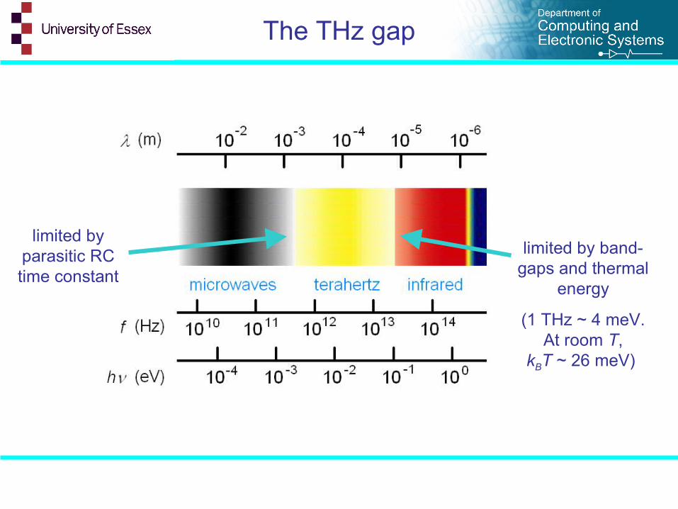
The THz gap
limited by parasitic RC time constant
limited by band-gaps and thermal
energy
(1 THz ~ 4 meV. At room T,
kBT ~ 26 meV)
Motivation
• High transmission for many materials
• Non-ionising
• THz chemical signatures (spectroscopy)
• THz radiation from space of interest
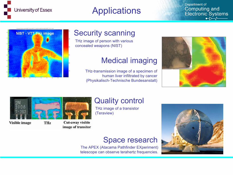
Applications
Medical imagingTHz-transmission image of a specimen of
human liver infiltrated by cancer (Physikalisch-Technische Bundesanstalt)
Security scanningTHz image of person with various concealed weapons (NIST)
Quality controlTHz image of a transistor(Teraview)
Space researchThe APEX (Atacama Pathfinder EXperiment) telescope can observe terahertz frequencies.
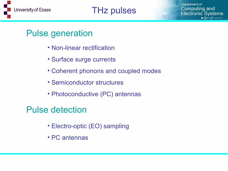
THz pulses
• Non-linear rectification
• Surface surge currents
• Coherent phonons and coupled modes
• Semiconductor structures
• Photoconductive (PC) antennas
Pulse generation
• Electro-optic (EO) sampling
• PC antennas
Pulse detection
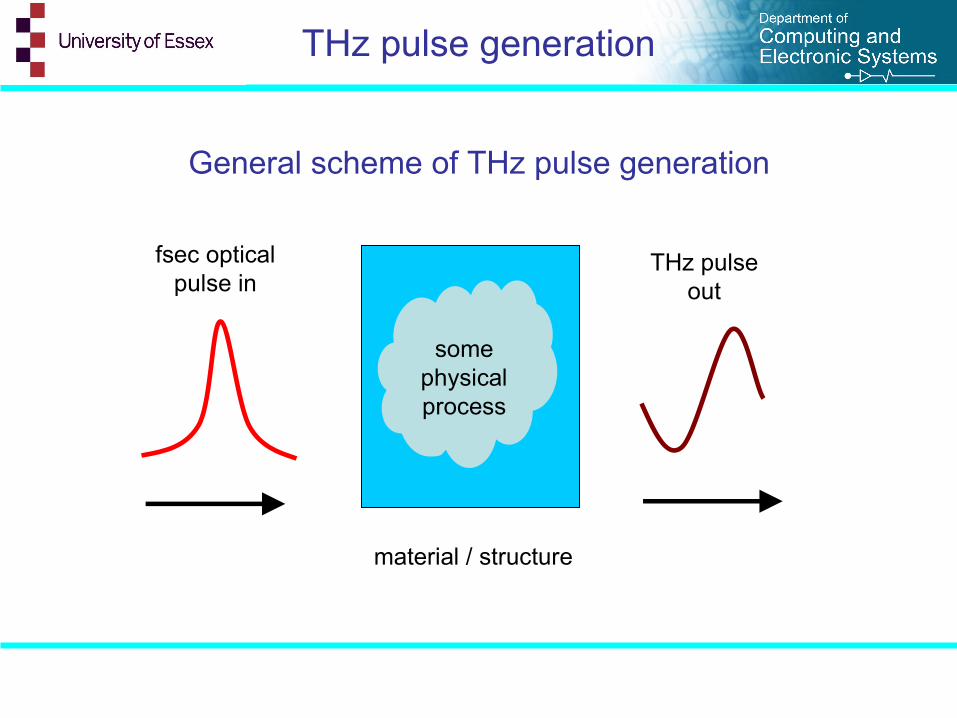
THz pulse generation
fsec optical pulse in
THz pulse out
some physical process
General scheme of THz pulse generation
material / structure
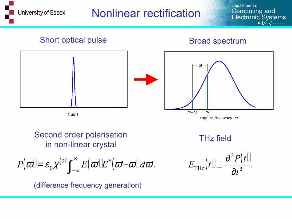
Nonlinear rectification
Short optical pulse Broad spectrum
Second order polarisation in non-linear crystal
( ) ( ) ( ) ( ) .''' *20 ∫
∞
∞−−= ωωωωχεω dEEP
THz field
( ) ( ).
2
2
THz t
tPtE
∂∂∝
(difference frequency generation)
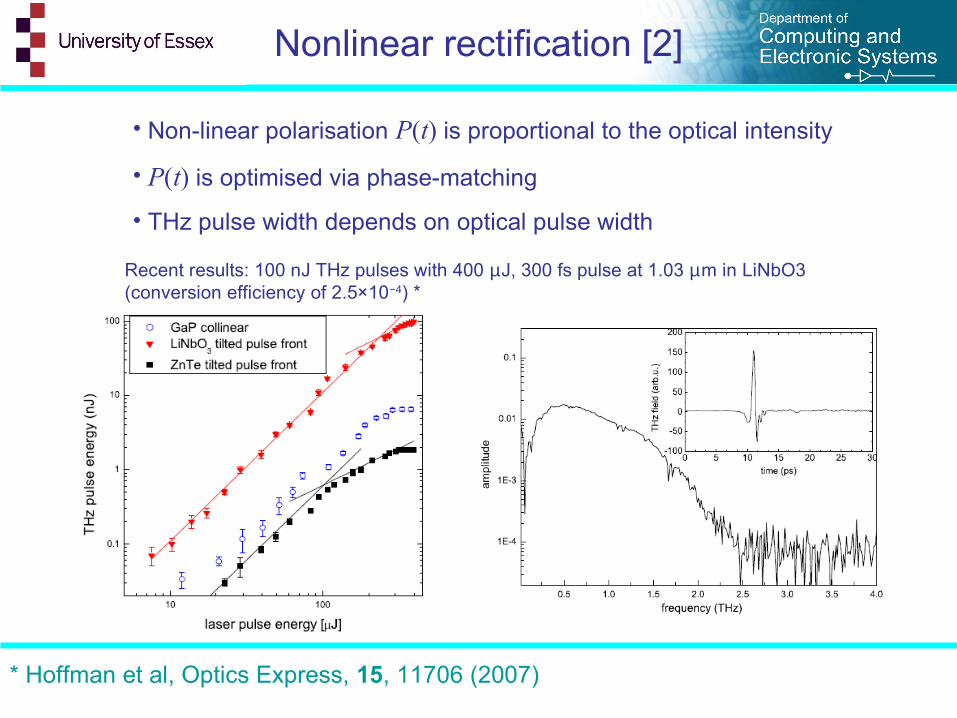
Nonlinear rectification [2]
• Non-linear polarisation P(t) is proportional to the optical intensity
• P(t) is optimised via phase-matching
• THz pulse width depends on optical pulse width
Recent results: 100 nJ THz pulses with 400 µJ, 300 fs pulse at 1.03 µm in LiNbO3 (conversion efficiency of 2.5×10⁻⁴) *
* Hoffman et al, Optics Express, 15, 11706 (2007)
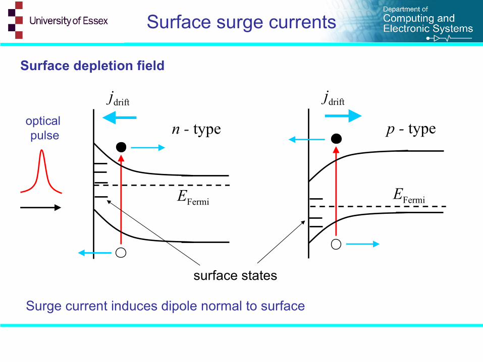
Surface surge currents
jdrift
EFermi
n - type
jdrift
EFermi
p - type
surface states
Surface depletion field
Surge current induces dipole normal to surface
optical pulse
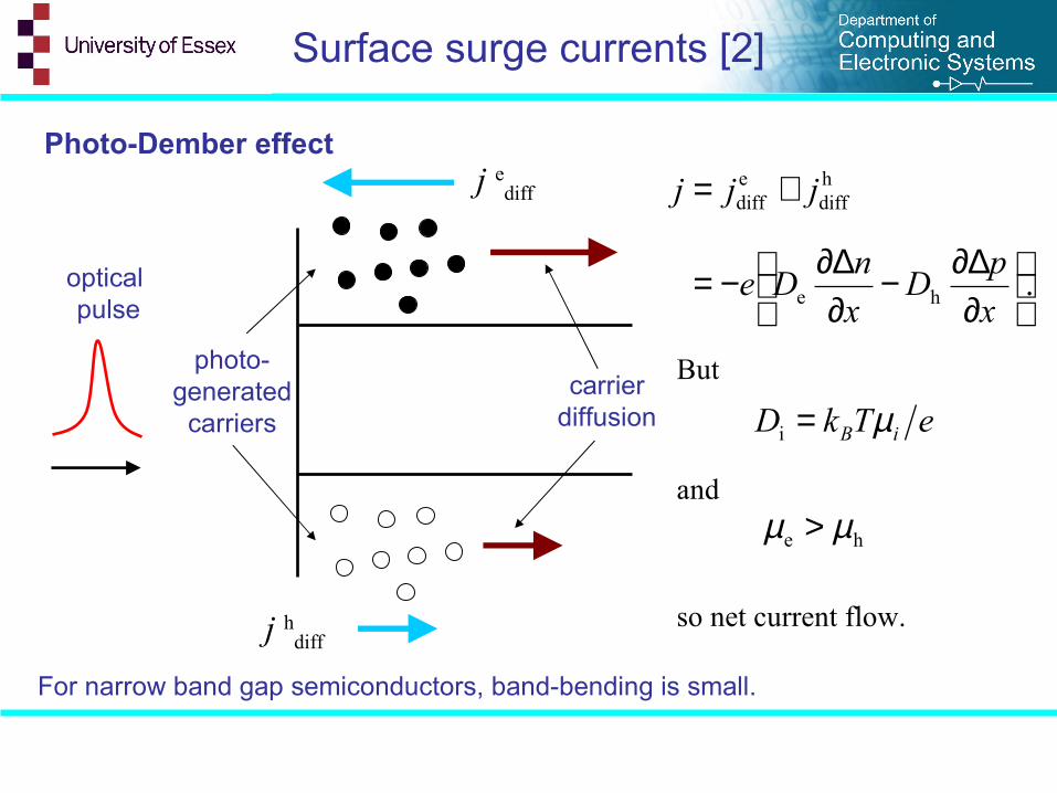
Surface surge currents [2]
Photo-Dember effect
carrier diffusion
photo-generated
carriers
j ediff
j hdiff
.he
hdiff
ediff
∂∆∂−
∂∆∂−=
+=
x
pD
x
nDe
jjj
eTkD iB µ=i
he µµ >
But
and
so net current flow.
For narrow band gap semiconductors, band-bending is small.
optical pulse
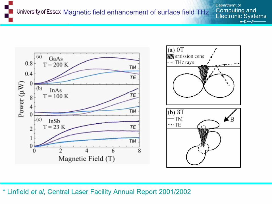
Magnetic field enhancement of surface field THz
* Linfield et al, Central Laser Facility Annual Report 2001/2002
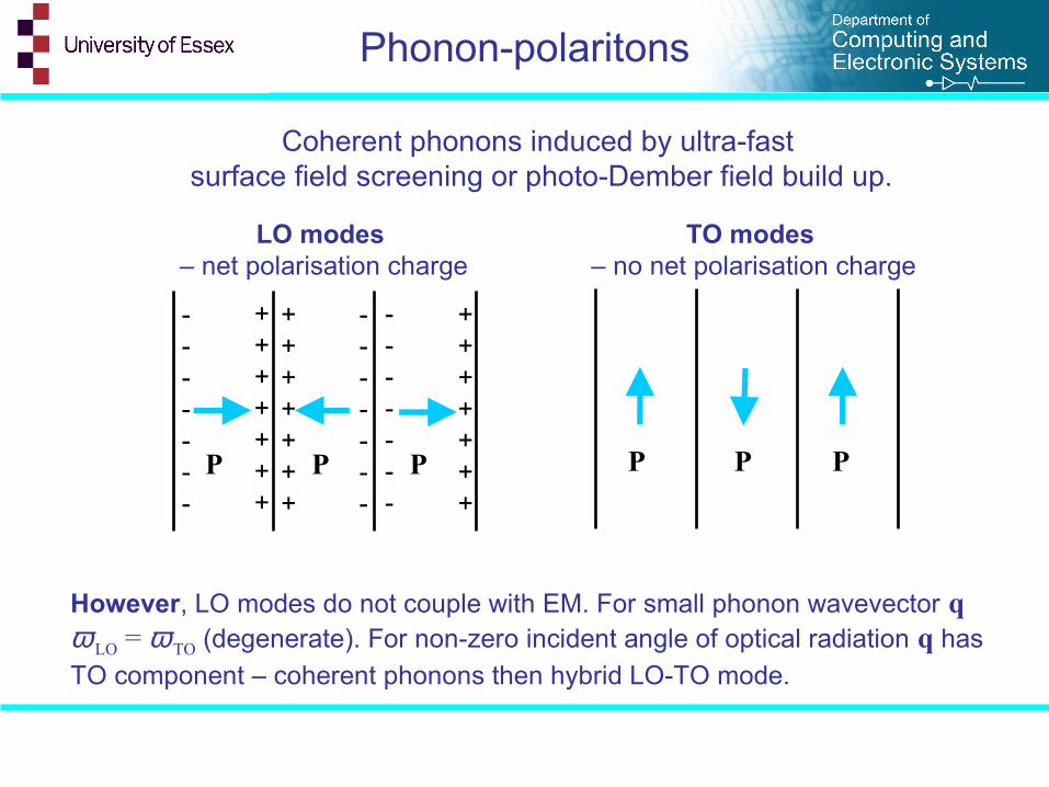
Phonon-polaritons
Coherent phonons induced by ultra-fast surface field screening or photo-Dember field build up.
+++++++
-------
+++++++
+++++++
-------
-------
P P P P P P
LO modes – net polarisation charge
TO modes – no net polarisation charge
However, LO modes do not couple with EM. For small phonon wavevector q ω LO = ω TO (degenerate). For non-zero incident angle of optical radiation q has
TO component – coherent phonons then hybrid LO-TO mode.
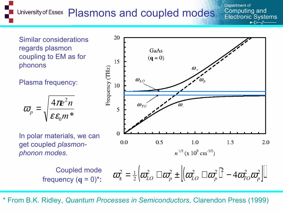
Plasmons and coupled modes
*
4
0
2
m
nep εε
πω =
Plasma frequency:
Coupled mode frequency (q = 0)*:
Similar considerations regards plasmon coupling to EM as for phonons
In polar materials, we can get coupled plasmon-phonon modes.
* From B.K. Ridley, Quantum Processes in Semiconductors, Clarendon Press (1999)
( )[ ]( )2222222212 4 pTOpLOpLO ωωωωωωω −+±+=±
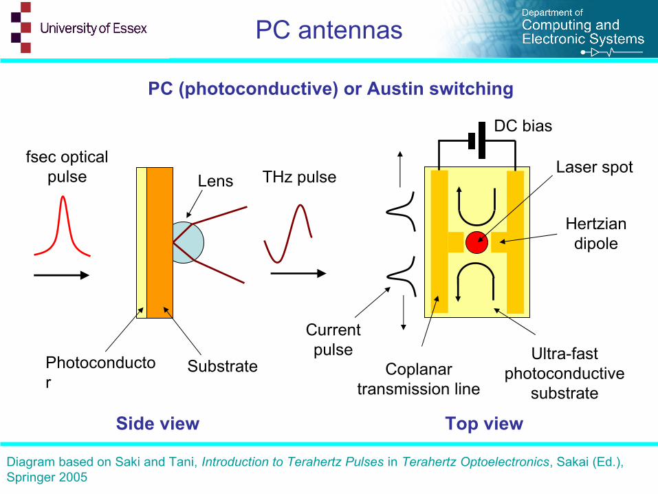
PC antennas
Current pulse
Coplanar transmission line
Ultra-fast photoconductive
substrate
Laser spot
Hertzian dipole
DC bias
Lens
SubstratePhotoconductor
fsec optical pulse THz pulse
Side view Top view
PC (photoconductive) or Austin switching
Diagram based on Saki and Tani, Introduction to Terahertz Pulses in Terahertz Optoelectronics, Sakai (Ed.), Springer 2005
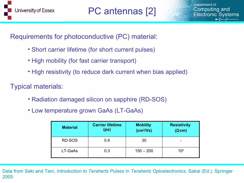
PC antennas [2]
Data from Saki and Tani, Introduction to Terahertz Pulses in Terahertz Optoelectronics, Sakai (Ed.), Springer 2005
Requirements for photoconductive (PC) material:
• Short carrier lifetime (for short current pulses)
• High mobility (for fast carrier transport)
• High resistivity (to reduce dark current when bias applied)
Typical materials:
• Radiation damaged silicon on sapphire (RD-SOS)
• Low temperature grown GaAs (LT-GaAs)
MaterialCarrier lifetime
(ps)Mobility (cm2/Vs)
Resistivity (Ωcm)
RD-SOS 0.6 30 -
LT-GaAs 0.3 150 – 200 106
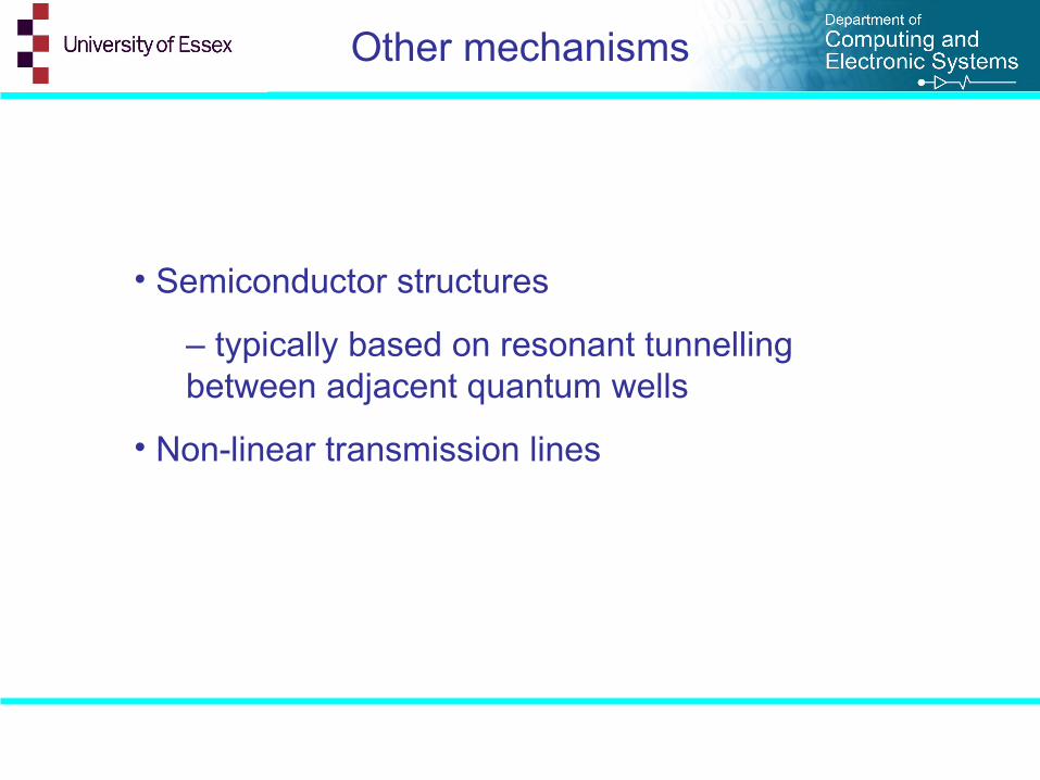
Other mechanisms
• Semiconductor structures
– typically based on resonant tunnelling between adjacent quantum wells
• Non-linear transmission lines
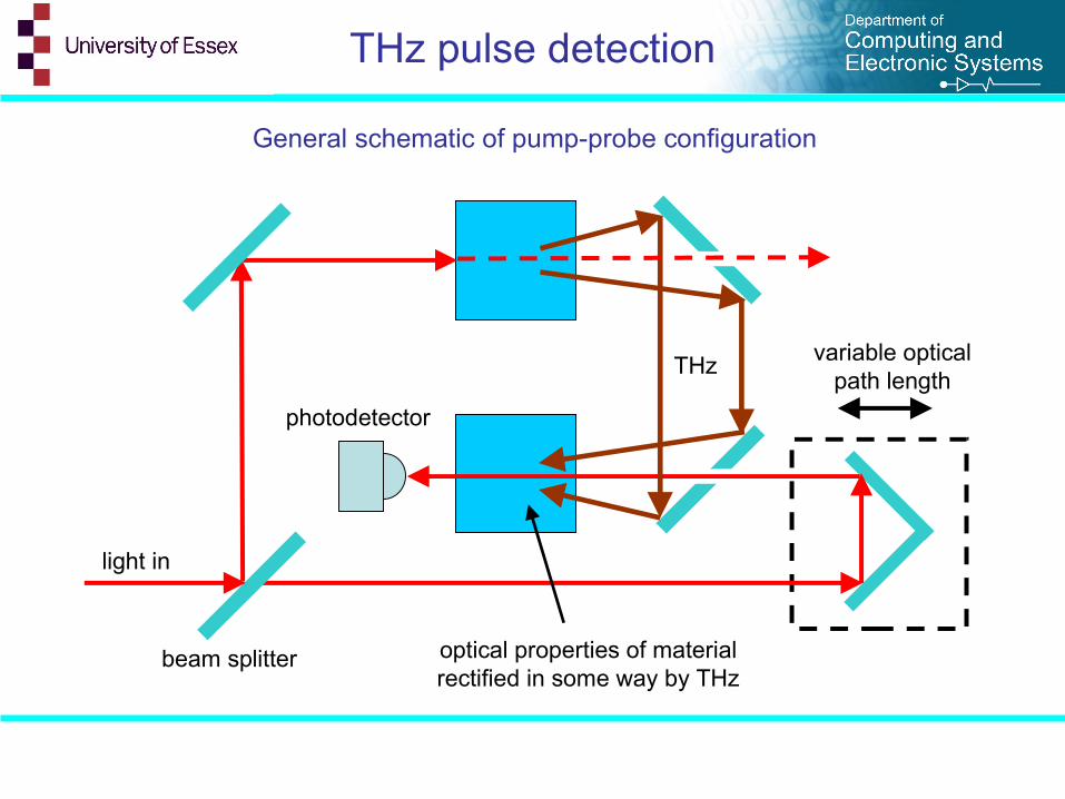
THz pulse detection
General schematic of pump-probe configuration
variable optical path length
beam splitter
light in
photodetector
THz
optical properties of material rectified in some way by THz
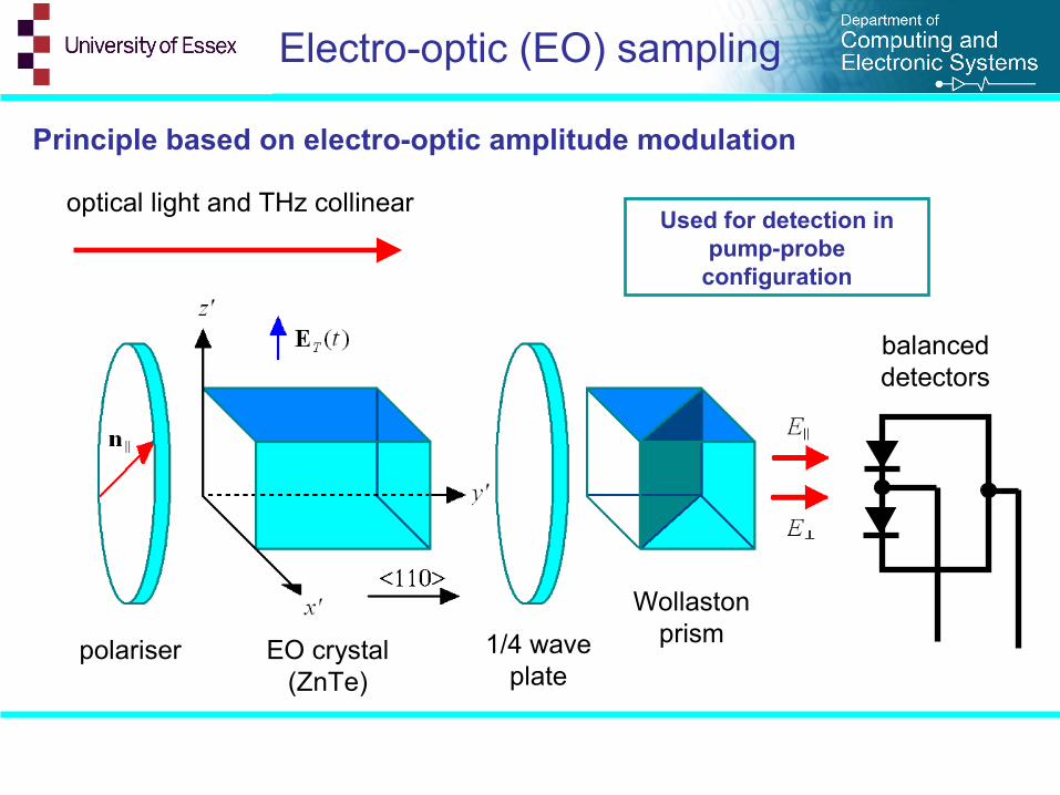
Electro-optic (EO) sampling
Principle based on electro-optic amplitude modulation
balanced detectors
Wollaston prism1/4 wave
plateEO crystal
(ZnTe)polariser
optical light and THz collinearUsed for detection in
pump-probe configuration
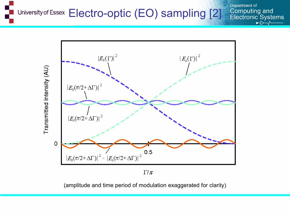
Electro-optic (EO) sampling [2]
(amplitude and time period of modulation exaggerated for clarity)
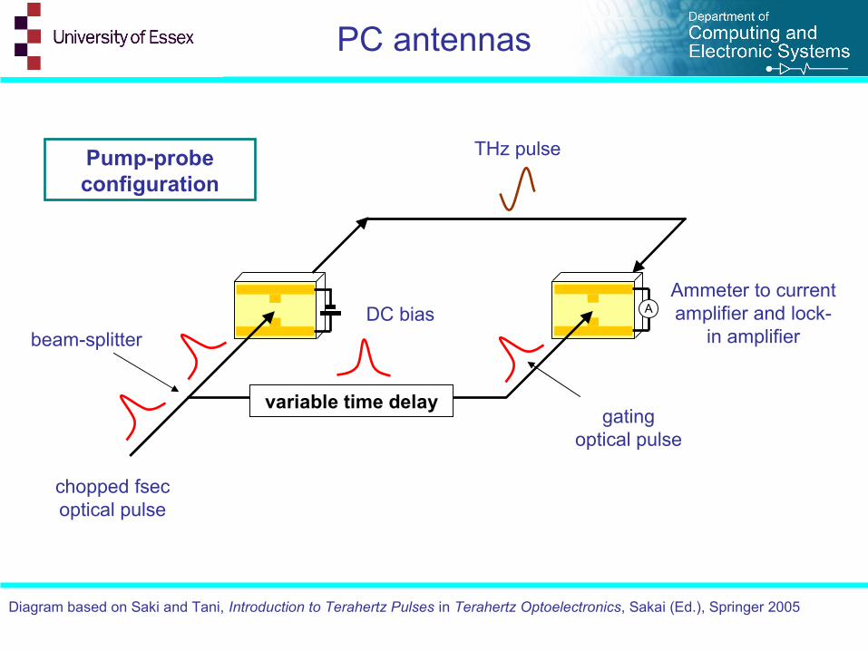
PC antennas
A
variable time delay
chopped fsec optical pulse
DC biasAmmeter to current amplifier and lock-
in amplifierbeam-splitter
gating optical pulse
THz pulse
Diagram based on Saki and Tani, Introduction to Terahertz Pulses in Terahertz Optoelectronics, Sakai (Ed.), Springer 2005
Pump-probe configuration
PC antennas [2]
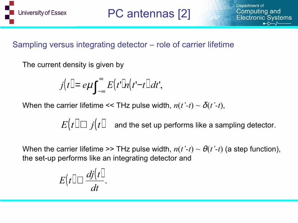
( ) ( ) ( ) ,'''∫∞
∞−−= dtttntEetj µ
When the carrier lifetime << THz pulse width, n(t’-t) ~ δ (t’-t),
( ) ( )tjtE ∝ and the set up performs like a sampling detector.
When the carrier lifetime >> THz pulse width, n(t’-t) ~ θ(t’-t) (a step function), the set-up performs like an integrating detector and
( ) ( ).
dt
tdjtE ∝
The current density is given by
Sampling versus integrating detector – role of carrier lifetime
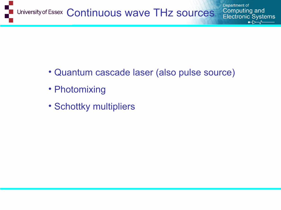
Continuous wave THz sources
• Quantum cascade laser (also pulse source)
• Photomixing
• Schottky multipliers
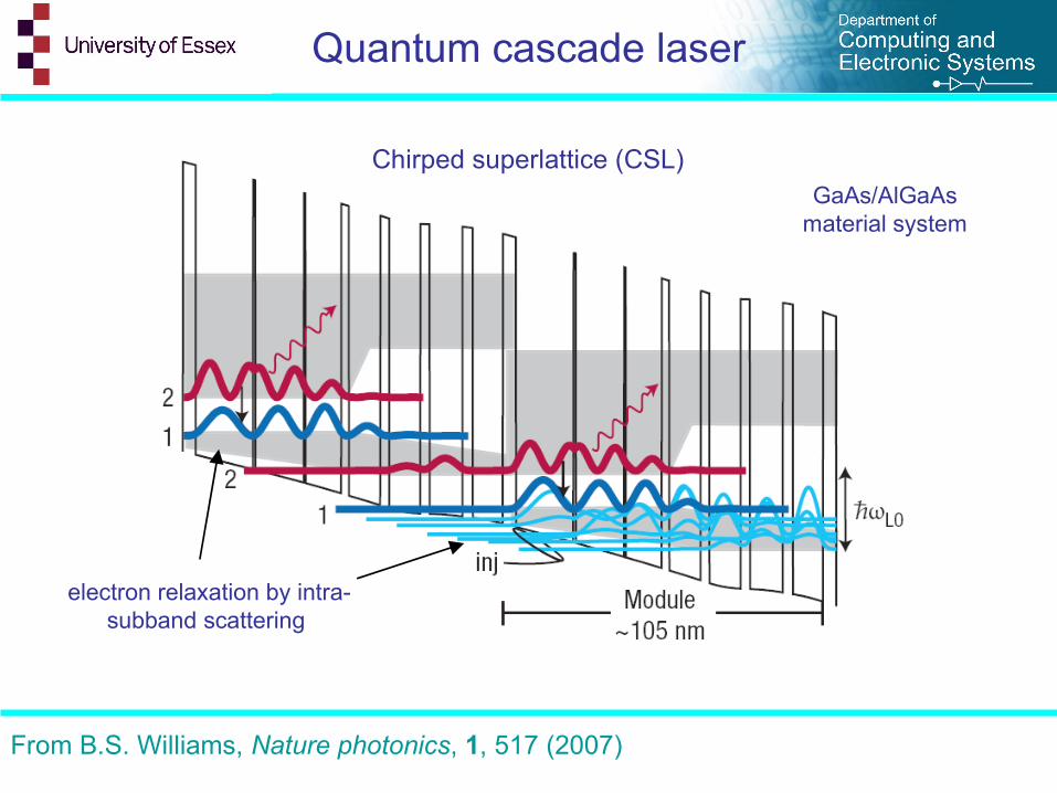
Quantum cascade laser
From B.S. Williams, Nature photonics, 1, 517 (2007)
electron relaxation by intra-subband scattering
Chirped superlattice (CSL)GaAs/AlGaAs
material system
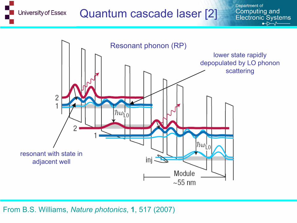
Quantum cascade laser [2]
From B.S. Williams, Nature photonics, 1, 517 (2007)
resonant with state in adjacent well
lower state rapidly depopulated by LO phonon
scattering
Resonant phonon (RP)
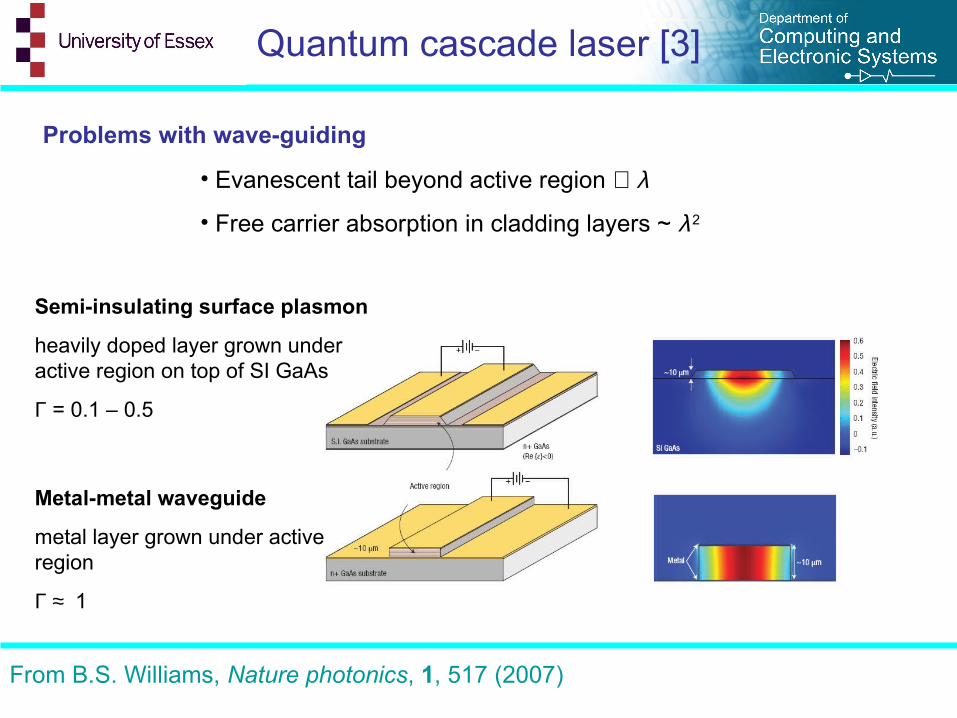
Quantum cascade laser [3]
From B.S. Williams, Nature photonics, 1, 517 (2007)
Problems with wave-guiding
• Evanescent tail beyond active region ∝ λ
• Free carrier absorption in cladding layers ~ λ2
Semi-insulating surface plasmon
heavily doped layer grown under active region on top of SI GaAs
Γ = 0.1 – 0.5
Metal-metal waveguide
metal layer grown under active region
Γ ≈ 1
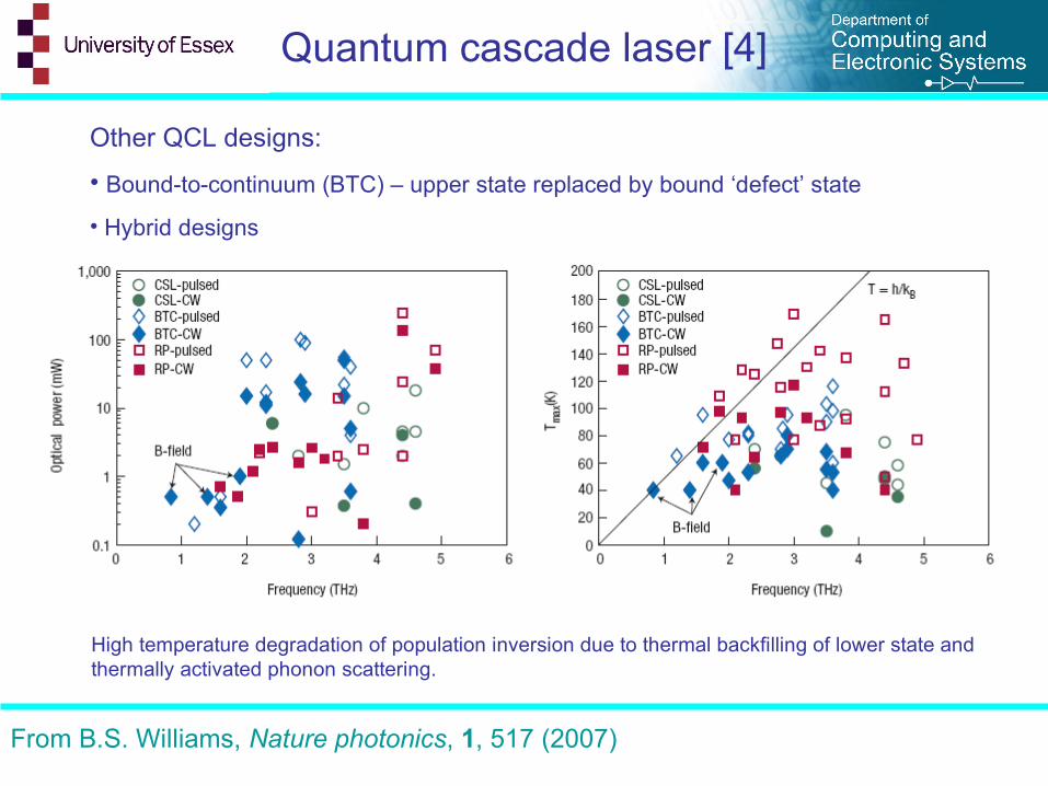
Quantum cascade laser [4]
From B.S. Williams, Nature photonics, 1, 517 (2007)
Other QCL designs:
• Bound-to-continuum (BTC) – upper state replaced by bound ‘defect’ state
• Hybrid designs
High temperature degradation of population inversion due to thermal backfilling of lower state and thermally activated phonon scattering.
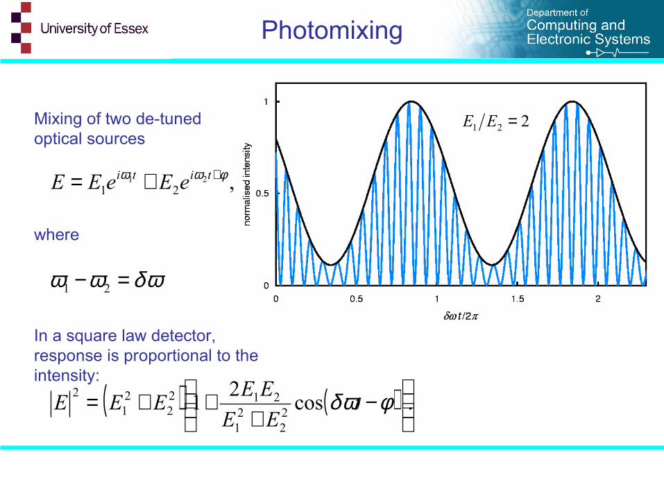
Photomixing
,2121
φωω ++= titi eEeEE
( ) ( ) .cos2
122
21
2122
21
2
−
+++= φδωt
EE
EEEEE
δωωω =− 21
Mixing of two de-tuned optical sources
where
In a square law detector, response is proportional to the intensity:
221 =EE
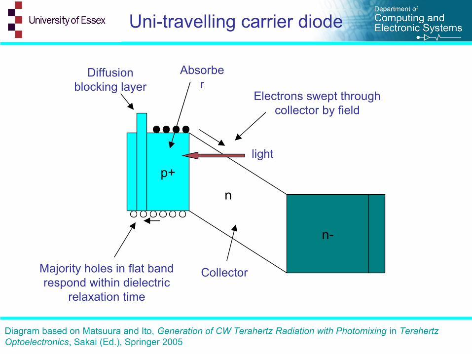
Uni-travelling carrier diode
p+
n-
n
Diffusion blocking layer
Absorber
Collector
light
Electrons swept through collector by field
Majority holes in flat band respond within dielectric
relaxation time
Diagram based on Matsuura and Ito, Generation of CW Terahertz Radiation with Photomixing in Terahertz Optoelectronics, Sakai (Ed.), Springer 2005
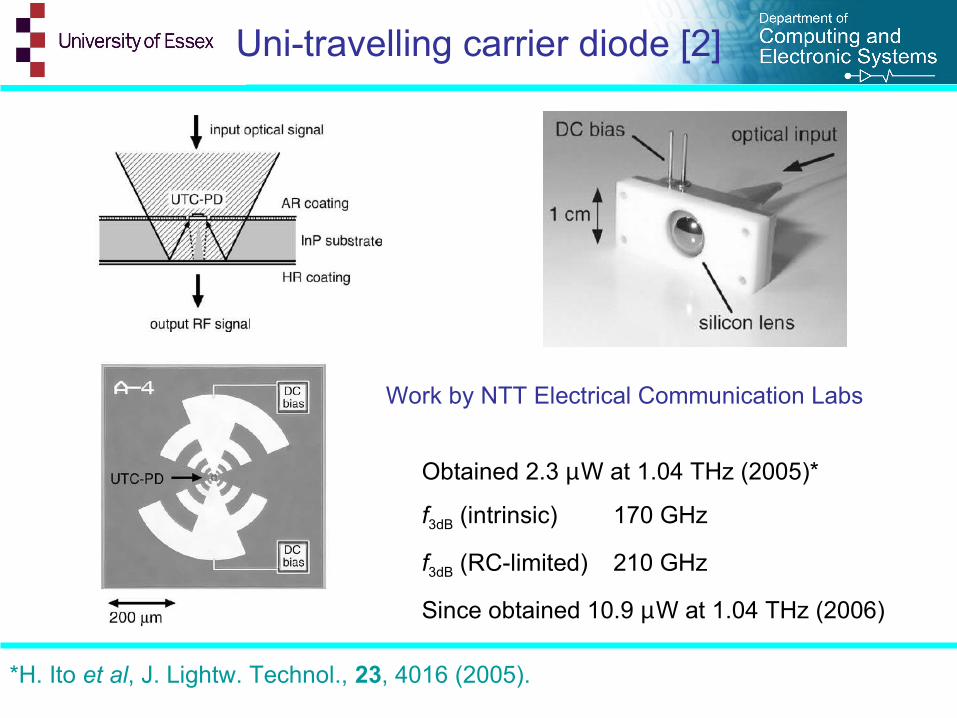
Uni-travelling carrier diode [2]
*H. Ito et al, J. Lightw. Technol., 23, 4016 (2005).
Work by NTT Electrical Communication Labs
Obtained 2.3 µW at 1.04 THz (2005)*
f3dB (intrinsic) 170 GHz
f3dB (RC-limited) 210 GHz
Since obtained 10.9 µW at 1.04 THz (2006)
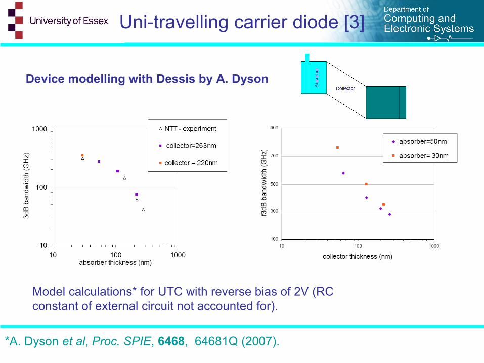
Uni-travelling carrier diode [3]
*A. Dyson et al, Proc. SPIE, 6468, 64681Q (2007).
Model calculations* for UTC with reverse bias of 2V (RC constant of external circuit not accounted for).
Device modelling with Dessis by A. Dyson
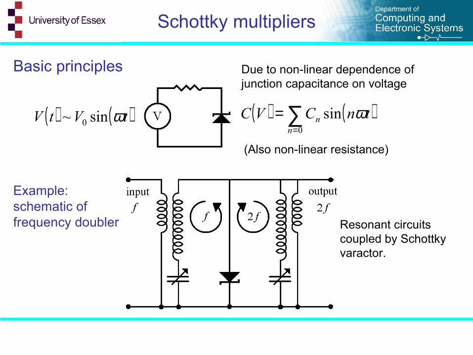
Schottky multipliers
( ) ( )tVtV ωsin~ 0( ) ( )∑
=
=0
sinn
n tnCVC ω
Due to non-linear dependence of junction capacitance on voltage
Basic principles
Example: schematic of frequency doubler Resonant circuits
coupled by Schottky varactor.
(Also non-linear resistance)
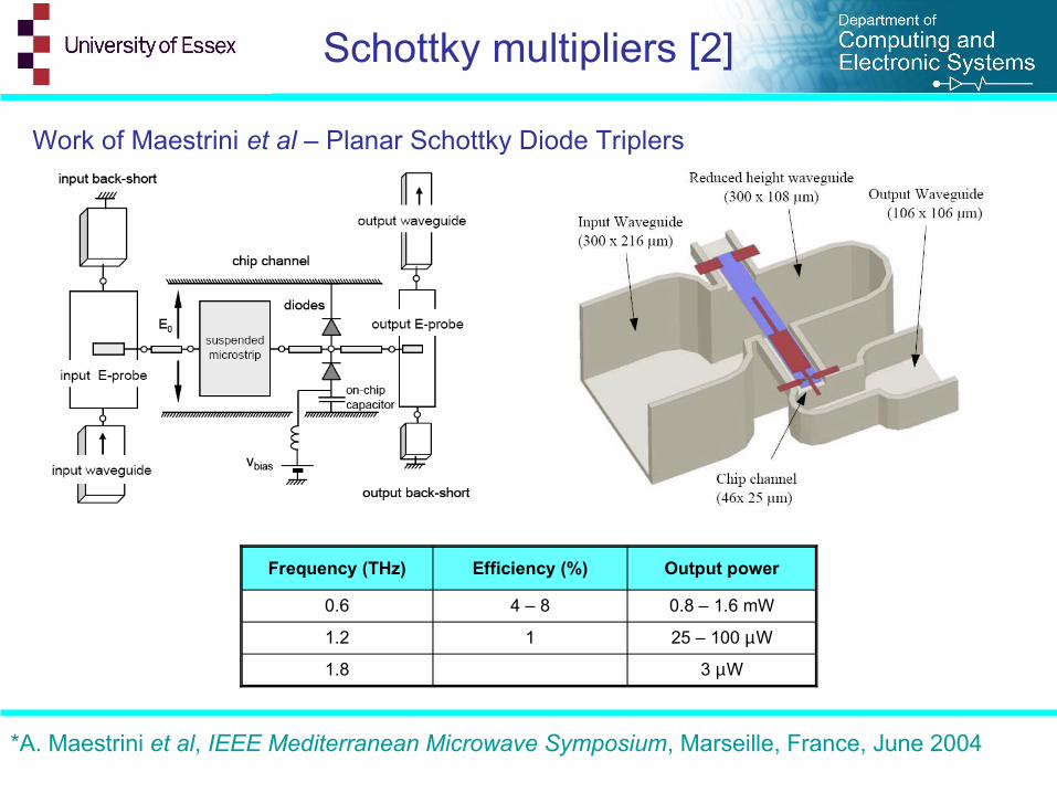
Schottky multipliers [2]
*A. Maestrini et al, IEEE Mediterranean Microwave Symposium, Marseille, France, June 2004
Work of Maestrini et al – Planar Schottky Diode Triplers
Frequency (THz) Efficiency (%) Output power
0.6 4 – 8 0.8 – 1.6 mW
1.2 1 25 – 100 µW
1.8 3 µW
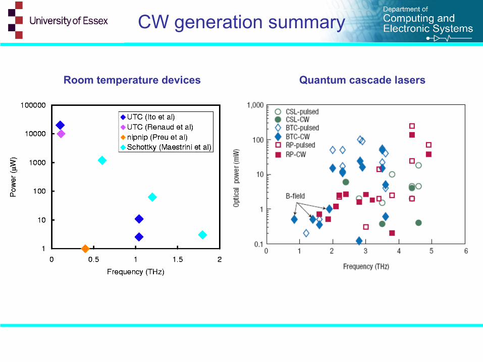
CW generation summary
Room temperature devices Quantum cascade lasers
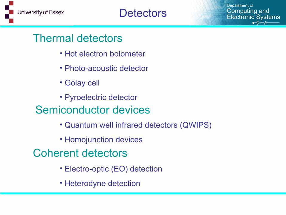
Detectors
• Hot electron bolometer
• Photo-acoustic detector
• Golay cell
• Pyroelectric detector
Thermal detectors
• Electro-optic (EO) detection
• Heterodyne detection
Coherent detectors
Semiconductor devices• Quantum well infrared detectors (QWIPS)
• Homojunction devices
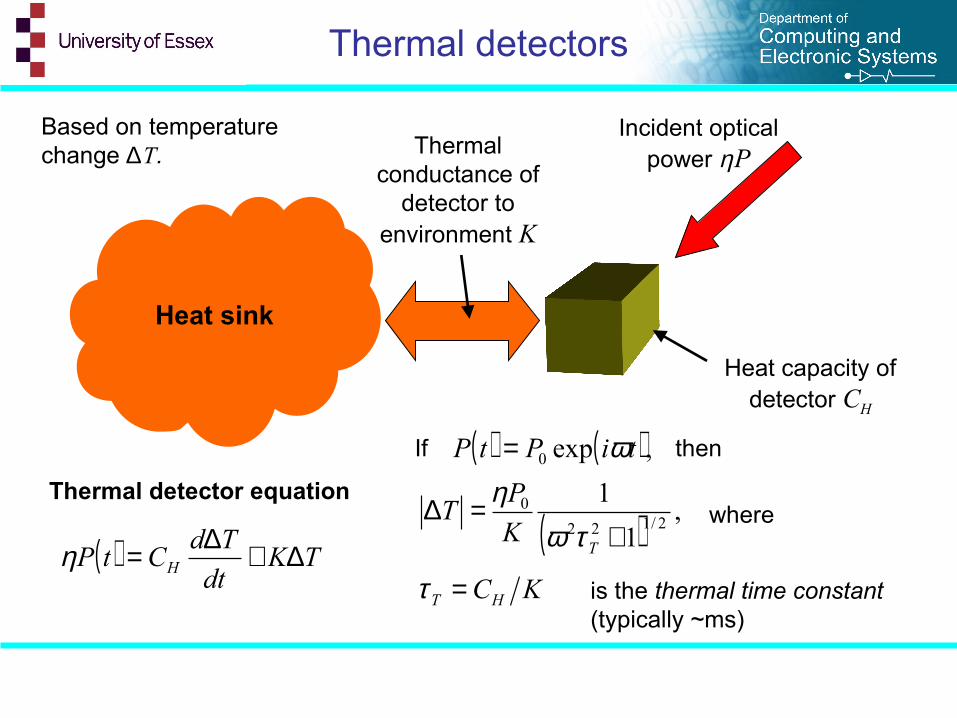
Thermal detectors
Heat sink
Thermal conductance of
detector to environment K
Heat capacity of detector CH
Incident optical power ηP
( ) TKdt
TdCtP H ∆+∆=η
( ) ( ),exp0 tiPtP ω=
( ) ,1
12/122
0
+=∆
TK
PT
τωη
KCHT =τ
Thermal detector equation
If then
where
is the thermal time constant(typically ~ms)
Based on temperature change ∆T.
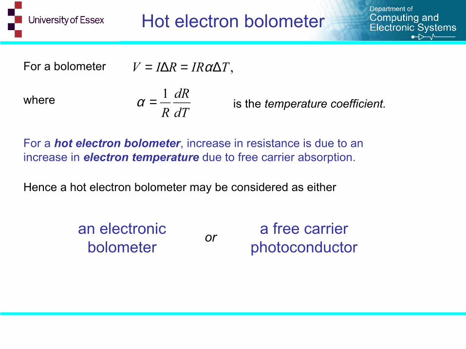
Hot electron bolometer
,TIRRIV ∆=∆= α
dT
dR
R
1=α
For a bolometer
where is the temperature coefficient.
For a hot electron bolometer, increase in resistance is due to an increase in electron temperature due to free carrier absorption.
Hence a hot electron bolometer may be considered as either
an electronic bolometer
a free carrier photoconductor
or
Hot electron bolometer [2]
• Resistance changes with increased electron temperature large, so high sensitivity
• Time constant related to electron relaxation time, so fast for thermal detector
• Requires cooling to liquid helium temperatures
But
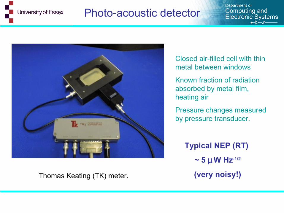
Photo-acoustic detector
Closed air-filled cell with thin metal between windows
Known fraction of radiation absorbed by metal film, heating air
Pressure changes measured by pressure transducer.
Thomas Keating (TK) meter.
Typical NEP (RT)
~ 5 µ W Hz-1/2
(very noisy!)
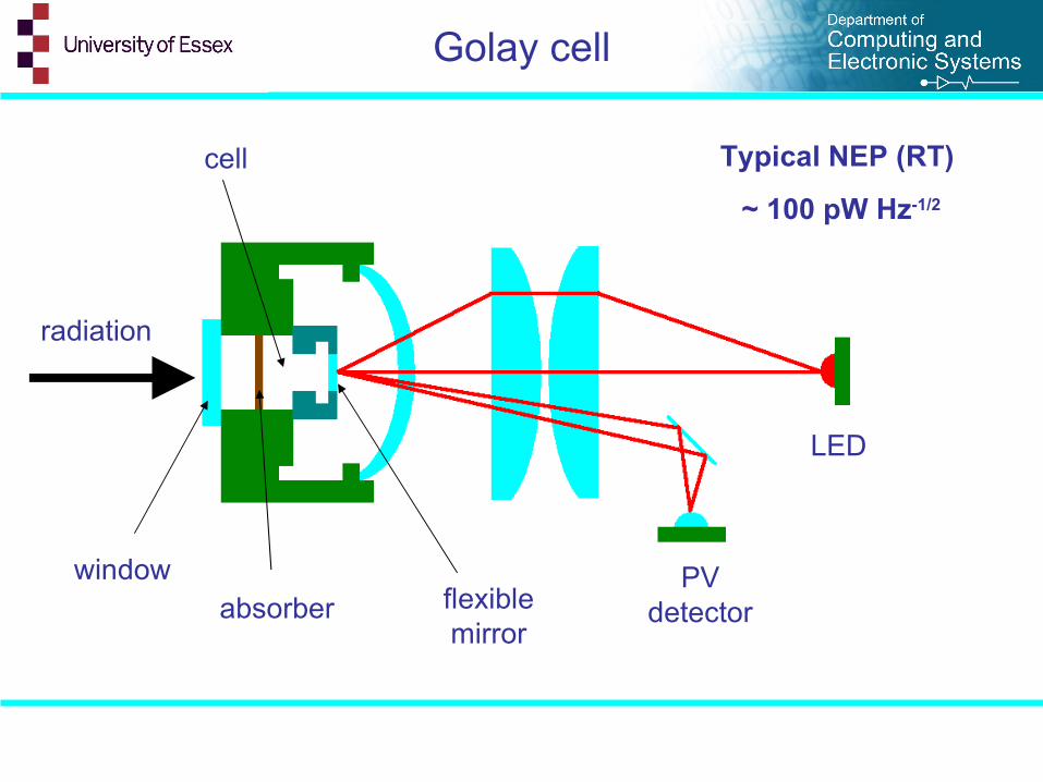
Golay cell
windowabsorber
cell
radiation
flexible mirror
LED
PV detector
Typical NEP (RT)
~ 100 pW Hz-1/2
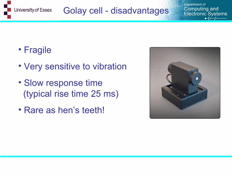
Golay cell - disadvantages
• Fragile
• Very sensitive to vibration
• Slow response time (typical rise time 25 ms)
• Rare as hen’s teeth!
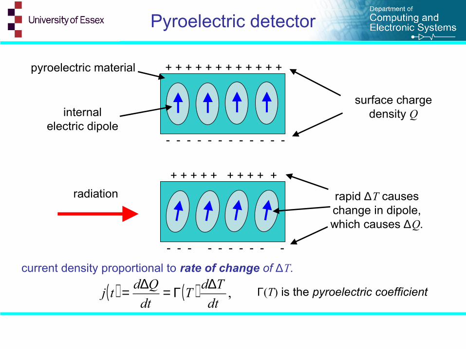
Pyroelectric detector
+ + + + + + + + + + + +
- - - - - - - - - - - -
+ + + + + + + + + +
- - - - - - - - - -
surface charge density Qinternal
electric dipole
rapid ∆T causes change in dipole, which causes ∆Q.
radiation
pyroelectric material
( ) ( ) ,dt
TdT
dt
Qdtj
∆Γ=∆= Γ(T) is the pyroelectric coefficient
current density proportional to rate of change of ∆T.
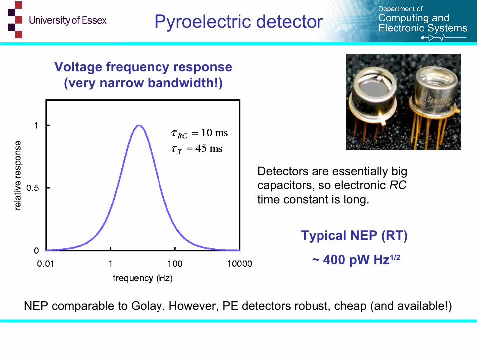
Pyroelectric detector
Detectors are essentially big capacitors, so electronic RC time constant is long.
Voltage frequency response(very narrow bandwidth!)
Typical NEP (RT)
~ 400 pW Hz1/2
NEP comparable to Golay. However, PE detectors robust, cheap (and available!)
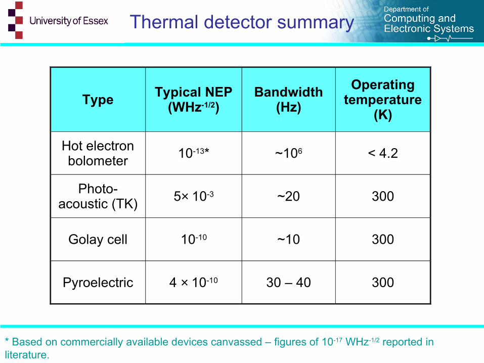
Thermal detector summary
TypeTypical NEP
(WHz-1/2)Bandwidth
(Hz)
Operating temperature
(K)
Hot electron bolometer
10-13* ~106 < 4.2
Photo-acoustic (TK) 5× 10⁻³ ~20 300
Golay cell 10-10 ~10 300
Pyroelectric 4 × 10⁻¹⁰ 30 – 40 300
* Based on commercially available devices canvassed – figures of 10-17 WHz-1/2 reported in literature.
Semiconductor devices
• Quantum well infrared detectors (QWIPS)
• Homojunction devices
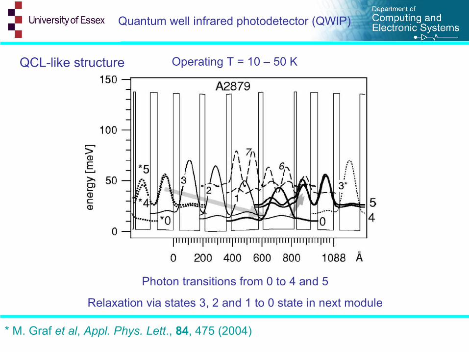
Quantum well infrared photodetector (QWIP)
* M. Graf et al, Appl. Phys. Lett., 84, 475 (2004)
QCL-like structure
Photon transitions from 0 to 4 and 5
Relaxation via states 3, 2 and 1 to 0 state in next module
Operating T = 10 – 50 K
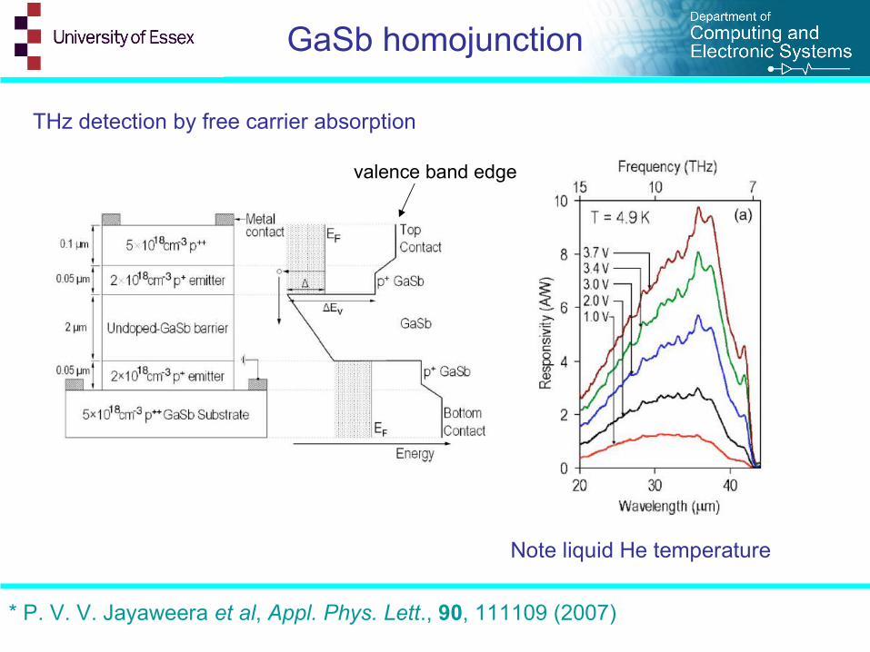
GaSb homojunction
THz detection by free carrier absorption
valence band edge
* P. V. V. Jayaweera et al, Appl. Phys. Lett., 90, 111109 (2007)
Note liquid He temperature
Coherent CW detectors
• Heterodyne detection using hot-electron bolometers with QCL as local oscillator
• Homodyne detection using the EO detection with photomixing
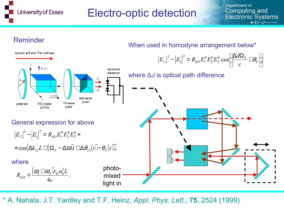
Electro-optic detection
Reminder
photo-mixed light in
( ) ( ) ( )( ),cos 1212
002
01
2
||
2
tttLk
EEEREE
TT
TEO
θθω −∆+∆−Ω+∆×
×=−⊥
( ).
4
304121
c
LnrREO
ωω +=
General expression for above
where
,cos 000
201
2
||
2
+Ω∆=−⊥ θ
c
dEEEREE T
TEO
When used in homodyne arrangement below*
where ∆d is optical path difference
* A. Nahata, J.T. Yardley and T.F. Heinz, Appl. Phys. Lett., 75, 2524 (1999)
Summary - sources
Terahertz pulses can be produced by
• Non-linear rectification
• Surface surge currents (surface depletion field and photo-Dember effects)
• Plasmon, phonon and coupled mode oscillations
• Austin or PC switching with micro-fabricated antennas
• Quantum cascade lasers (require cooling)
Terahertz CW can be produced by
• Photomixing (PC switching or using UTC)
• Schottky multiplier chains
• Quantum cascade lasers (require cooling)
Summary - detectors
Terahertz pulses can be detected by
• Electro-optic effect (in pump-probe configuration)
• PC antennas (in pump-probe configuration)
• Thermal detectors (usually hot electron bolometer)
Terahertz CW can be detected by
• Thermal detectors (HEBs need cooling)
• Semiconductor devices (need cooling)
• Electro-optic effect
• Heterodyning using QCL as a local oscillator (needs cooling)
Cheap, portable room temperature devices
Best performance technologies often need cooling and are not easy to implement in portable devices.
Possible candidates for compact room temperature sources:
• UTC integrated with lasers
• Schottky multiplier chains
Possible candidates for robust room temperature detectors:
• Photo-acoustic detectors (although very noisy)
• Pyroelectric detectors (very slow)
• Heterodyne detectors using Schottky multiplier chains
• Electro-optic effect?