Embed Size (px)
Citation preview

Test Vector Extraction Methodology For Power Integrity Analysis
Master of Science Thesis in Integrated Electronic System Design
MARTIN OLSSON
Chalmers University of TechnologyDepartment of Computer Science and EngineeringGöteborg, Sweden, June 2010

The Author grants to Chalmers University of Technology the non-exclusive right to publish the Work electronically and in a non-commercial purpose make it accessible on the Internet. The Author warrants that he/she is the author to the Work, and warrants that the Work does not contain text, pictures or other material that violates copyright law.
The Author shall, when transferring the rights of the Work to a third party (for example a publisher or a company), acknowledge the third party about this agreement. If the Author has signed a copyright agreement with a third party regarding the Work, the Author warrants hereby that he/she has obtained any necessary permission from this third party to let Chalmers University of Technology store the Work electronically and make it accessible on the Internet.
Test Vector Extraction MethodologyFor Power Integrity Analysis
MARTIN OLSSON
© MARTIN OLSSON, June 2010.
Examiner: Prof. Per Larsson-Edefors
Chalmers University of TechnologyDepartment of Computer Science and EngineeringSE-412 96 GöteborgSwedenTelephone + 46 (0)31-772 1000
Cover:A 32-bit microprocessor power grid with the supply voltage deviation at the found maximum, along with time-domain representation of voltage fluctuation at the worst node.
Department of Computer Science and EngineeringGöteborg, Sweden, June 2010
TEST VECTOR EXTRACTION METHODOLOGY FOR
POWER INTEGRITY ANALYSIS
Martin Olsson
Department of Computer Science and Engineering
Chalmers University of Technology
Goteborg, Sweden 2010

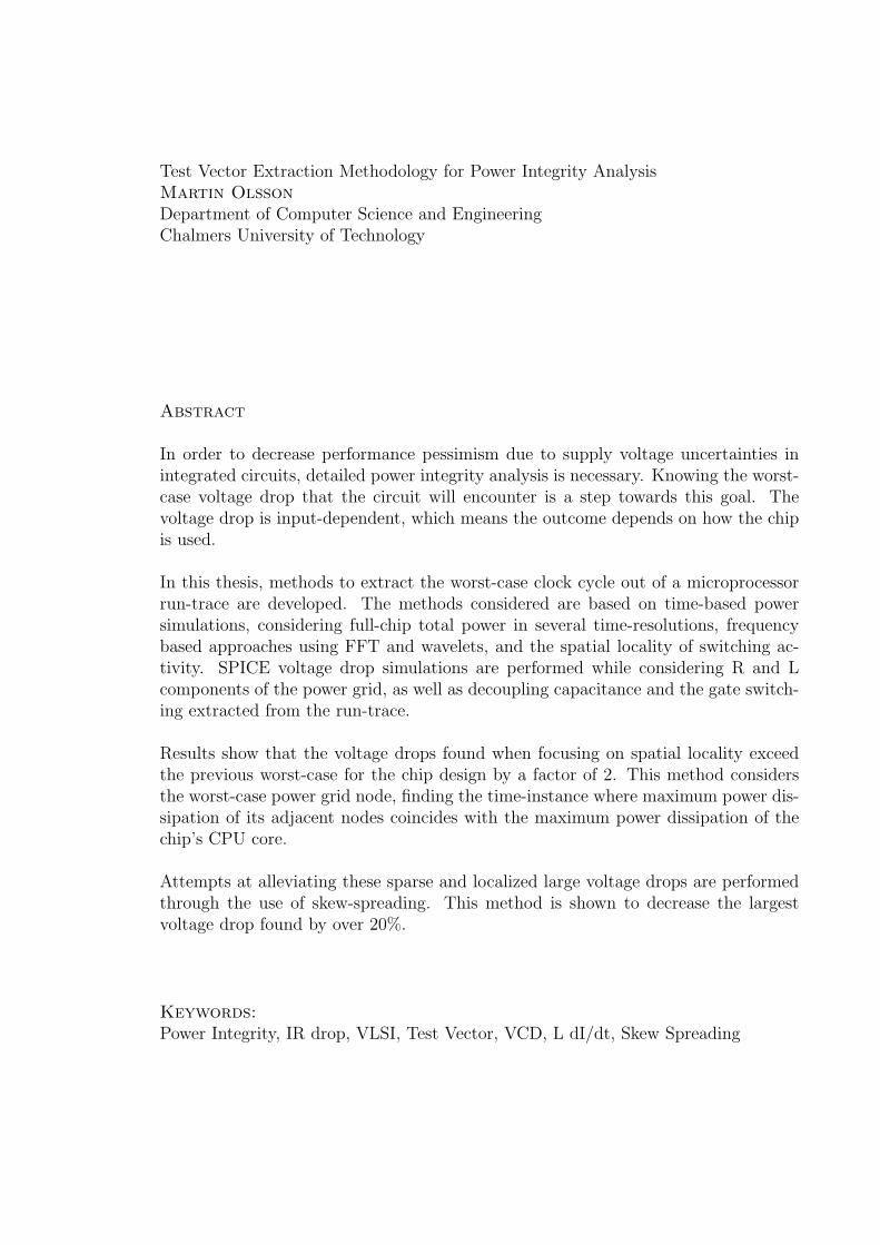
Test Vector Extraction Methodology for Power Integrity AnalysisMartin Olsson
Department of Computer Science and EngineeringChalmers University of Technology
Abstract
In order to decrease performance pessimism due to supply voltage uncertainties inintegrated circuits, detailed power integrity analysis is necessary. Knowing the worst-case voltage drop that the circuit will encounter is a step towards this goal. Thevoltage drop is input-dependent, which means the outcome depends on how the chipis used.
In this thesis, methods to extract the worst-case clock cycle out of a microprocessorrun-trace are developed. The methods considered are based on time-based powersimulations, considering full-chip total power in several time-resolutions, frequencybased approaches using FFT and wavelets, and the spatial locality of switching ac-tivity. SPICE voltage drop simulations are performed while considering R and Lcomponents of the power grid, as well as decoupling capacitance and the gate switch-ing extracted from the run-trace.
Results show that the voltage drops found when focusing on spatial locality exceedthe previous worst-case for the chip design by a factor of 2. This method considersthe worst-case power grid node, finding the time-instance where maximum power dis-sipation of its adjacent nodes coincides with the maximum power dissipation of thechip’s CPU core.
Attempts at alleviating these sparse and localized large voltage drops are performedthrough the use of skew-spreading. This method is shown to decrease the largestvoltage drop found by over 20%.
Keywords:
Power Integrity, IR drop, VLSI, Test Vector, VCD, L dI/dt, Skew Spreading


Contents
List of Figures vii
List of Tables viii
Dedication ix
Acknowledgments xi
1 Background 11.1 Power Integrity Analysis . . . . . . . . . . . . . . . . . . . . . . . . . 2
1.1.1 Static IR Drop, Dynamic IR Drop and Power Integrity . . . . 21.2 The Power Grid and Chip Design Under Study . . . . . . . . . . . . 3
1.2.1 The Power Grid Model . . . . . . . . . . . . . . . . . . . . . . 41.2.2 Modeling Switching Information . . . . . . . . . . . . . . . . . 5
1.3 The Choice of Test Vectors . . . . . . . . . . . . . . . . . . . . . . . . 61.3.1 Test Vector Extraction . . . . . . . . . . . . . . . . . . . . . . 61.3.2 The PrimeTime PX Power Trace Waveform file . . . . . . . . 9
1.4 Results of Previous Research . . . . . . . . . . . . . . . . . . . . . . . 10
2 Methods for Test Vector Extraction 112.1 Power Analysis in PrimeTime PX . . . . . . . . . . . . . . . . . . . . 12
2.1.1 Total Power Analysis . . . . . . . . . . . . . . . . . . . . . . . 122.1.2 Extracting Local Power Trace Information . . . . . . . . . . . 13
2.2 Spatial Locality . . . . . . . . . . . . . . . . . . . . . . . . . . . . . . 142.2.1 Combining localities to find worst-case vectors . . . . . . . . . 162.2.2 Finding Worst Node on Chip . . . . . . . . . . . . . . . . . . 18
2.3 Frequency Domain . . . . . . . . . . . . . . . . . . . . . . . . . . . . 282.3.1 Finding the chip resonant frequencies . . . . . . . . . . . . . . 292.3.2 FFT based approaches . . . . . . . . . . . . . . . . . . . . . . 302.3.3 Wavelet based approaches . . . . . . . . . . . . . . . . . . . . 30
2.4 Cell-level Power Information . . . . . . . . . . . . . . . . . . . . . . . 322.4.1 Types of Cells Distribution for Test Vectors . . . . . . . . . . 33
v

2.4.2 Alleviating Simultaneous Switching Noise Through Skew Spread-ing . . . . . . . . . . . . . . . . . . . . . . . . . . . . . . . . . 36
3 Results 383.1 Full-chip Maximum Power . . . . . . . . . . . . . . . . . . . . . . . . 383.2 Frequency and dP/dt based approaches . . . . . . . . . . . . . . . . . 413.3 Localized Voltage drops: Finding the Where and When . . . . . . . . 43
3.3.1 Choosing the Worst Node . . . . . . . . . . . . . . . . . . . . 453.4 Voltage Drop Characteristics and Worst-case . . . . . . . . . . . . . . 49
3.4.1 The effect of on-chip inductance on voltage drop . . . . . . . . 513.4.2 Chip-wide distribution of voltage drop . . . . . . . . . . . . . 53
3.5 On-chip Inductance and Bond-wire Inductance . . . . . . . . . . . . . 553.5.1 Frequency Components and Inductance Contributions . . . . . 59
3.6 Results of Skew-Spreading on Voltage Drop . . . . . . . . . . . . . . 60
4 Discussion 634.1 Weaknesses in Model and Methodology . . . . . . . . . . . . . . . . . 634.2 Timing implications . . . . . . . . . . . . . . . . . . . . . . . . . . . . 644.3 Consequences for design flow . . . . . . . . . . . . . . . . . . . . . . . 664.4 Conclusions . . . . . . . . . . . . . . . . . . . . . . . . . . . . . . . . 67
Bibliography 68
vi

List of Figures
1.1 Power Grid of the Chip Design Studied . . . . . . . . . . . . . . . . . 41.2 Workflow of Current Source Generation . . . . . . . . . . . . . . . . . 71.3 The powergrid model in two layers . . . . . . . . . . . . . . . . . . . 82.1 Illustrating the relationship between units and nodes . . . . . . . . . 142.2 Illustrating nodes and adjacent nodes . . . . . . . . . . . . . . . . . . 152.3 Linear fit of current to voltage drop . . . . . . . . . . . . . . . . . . . 162.4 Overlapping top-list entries 100ns List index . . . . . . . . . . . . . . 182.5 Total power dissipation per node . . . . . . . . . . . . . . . . . . . . 202.6 Maximum power per node, timescale 1 ns . . . . . . . . . . . . . . . . 222.7 Power for adjacent nodes at node power maximum, timescale 1 ns . . 232.8 Maximum power per node, timescale 0.1 ns . . . . . . . . . . . . . . . 252.9 Power for adjacent nodes at node power maximum, timescale 0.1 ns . 262.10 Power for CPU nodes at node power maximum, timescale 0.1 ns . . . 272.11 Impedance of on-chip power grid . . . . . . . . . . . . . . . . . . . . 292.12 Scalogram of wavelet transform, 1 ns resolution full-chip power trace . 312.13 Voltage Drop with different components highlighted . . . . . . . . . . 342.14 Voltage Drop with different components highlighted, worst-case drop 353.1 Full-chip power over time . . . . . . . . . . . . . . . . . . . . . . . . . 403.2 Current signatures for nodes 62 and 64. Time window at node 62
power peak. . . . . . . . . . . . . . . . . . . . . . . . . . . . . . . . . 473.3 Current signatures for nodes 62 and 64. Time window at node 64
power peak. . . . . . . . . . . . . . . . . . . . . . . . . . . . . . . . . 483.4 Voltage Drop for worst node . . . . . . . . . . . . . . . . . . . . . . . 513.5 Voltage drop for worst node, without on-chip inductance . . . . . . . 533.6 Voltage drop magnitude distribution . . . . . . . . . . . . . . . . . . 543.7 Voltage drop by node location . . . . . . . . . . . . . . . . . . . . . . 553.8 Bond-wire vs on-chip inductance for two randomly selected nodes . . 573.9 Bond-wire vs on-chip inductance for two nodes . . . . . . . . . . . . . 583.10 Frequency break-down of Bond-wire vs On-chip inductance . . . . . . 603.11 Voltage drop for worst-case node, with and without skew-spreading . 613.12 Effect of skew-spreading on current profiles . . . . . . . . . . . . . . . 624.1 Datapath with launch and capture flip-flops . . . . . . . . . . . . . . 64
vii

List of Tables
2.1 File size for waveform files by resolution . . . . . . . . . . . . . . . . 132.2 Correlation coefficient of voltage drop to current properties . . . . . . 162.3 Switching Cell Types in a Voltage Drop . . . . . . . . . . . . . . . . . 342.4 Switching Cell Types in a worst-case Voltage Drop . . . . . . . . . . 352.5 Switching Cell Types in a Voltage Drop . . . . . . . . . . . . . . . . . 363.1 Total Power Approach, time resolution Vs maximum voltage drop . . 393.2 Voltage drop of randomly selected test vectors . . . . . . . . . . . . . 413.3 Voltage drop of dP/dt-based vectors . . . . . . . . . . . . . . . . . . 413.4 Voltage drop of FFT-based vectors . . . . . . . . . . . . . . . . . . . 423.5 Voltage drop of wavelet-based vectors . . . . . . . . . . . . . . . . . . 433.6 Localized power results . . . . . . . . . . . . . . . . . . . . . . . . . . 443.7 Localized power results, overlapping . . . . . . . . . . . . . . . . . . 443.8 CPU and adjacent nodes overlapping time windows, Voltage Drops . 453.9 Test vectors found by considering each node’s power maximum . . . . 483.10 Current profile max of two test vectors [A] . . . . . . . . . . . . . . . 503.11 Bond-L vs. On-Chip L, number of dominating nodes per metal layer . 583.12 Bond-L vs. On-Chip L, number of dominating nodes per frequency
component . . . . . . . . . . . . . . . . . . . . . . . . . . . . . . . . . 60
viii

Dedication
To Annasofia.
ix

x

Acknowledgments
I would like to thank my examiner at Chalmers - Per Larsson-Edefors - and mysupervisors at Atmel Norway - Johnny Pihl and Daniel Andersson.
xi

xii

Chapter 1
Background
Power integrity analysis deals with verifying the power supply grid of an integratedcircuit. In order to gain a greater understanding of what happens in the on-chippower grid, research work has been devoted to this field as prior work leading up tothis master’s thesis.
With increased understanding it is hoped to be possible to move away from thepessimism introduced by the standard practice of corner-based design, where the per-formance of an integrated circuit is limited by the variability of the Process, Voltageand Temperature (PVT) variables.
In the prior work, a detailed model of the power supply grid of a 32-bit microprocessorwas developed. Several research papers ([1] [2] [3] [4] [5]) have been published usingthe developed model, analyzing power integrity issues from different perspectives.
While this model is input-dependent, and the outcome of analyses made could bedifferent for different input patterns, only one assumed worst-case stimulus has beenused. Thus, there is a gap in the methodology of analyzing power integrity issueswith this model.
Specifically, one clock cycle has been used under the assumption that it will causethe largest problems for power integrity. Realizing that this might not necessarily bethe case, the goal of this master’s thesis is to investigate the space of possible inputstimuli, and develop a methodology to extract the worst-case clock cycle, defined hereas the clock cycle resulting in the largest observed supply voltage deviation from thenominal value.
Starting with a primer on power integrity analysis, this chapter will then describe thepower grid model considered, and the methodology of power integrity analysis in this
1

2
context. Chapter 2 will present methodologies of worst-case test vector extractiondeveloped in the work of this thesis, and the results will be presented in chapter 3.
1.1 Power Integrity Analysis
The on-chip power supply grid of an integrated circuit must be designed carefully tobe able to support the switching gates with a stable voltage. Any deviation from thenominal voltage leads to increased gate delay and might cause the chip to malfunc-tion. Since the metal carrying the current has a finite conductivity, a large currentwill lead to a voltage drop according to Ohm’s law, V = IR. Power grid wires can,of course, be made wider to reduce resistance, but it comes at the cost of increasedrouting congestion. The other standard way to deal with IR drop is to add decou-pling capacitances. These act as temporary repositories of charge that can feed theirnearby gates, and are implemented on-chip using transistors. [6] is a good resourceon this subject.
Ensuring that a chip design’s power grid will satisfy its current demand is known aspower integrity analysis. It is an important step in any chip design sign-off stage, butrecent years miniaturization of integrated circuits comes with new issues that mustbe considered.
A supply voltage drop is dominated by two terms, such that the voltage drop can bedescribed as V = IR+ LdI/dt. The first term, or IR-Drop, has been the main focusof traditional power integrity analysis.
While the parasitic inductance, L, in the on-chip power grid and the bond wires con-necting the die to the package has always been present, dI/dt has traditionally beennegligible. However, as feature-sizes in integrated circuits become smaller with eachnew process node, transition times become shorter and the LdI/dt term becomesmore important due to the faster current rate-of-change.
Technology trends have also gone towards decreasing the supply voltage in order toreduce power dissipation. This makes power integrity analysis still more critical, sincethe noise margin of the power supply decreases when the difference between the sup-ply voltage and the threshold voltage of the transistors, Vt, decreases [7].
1.1.1 Static IR Drop, Dynamic IR Drop and Power Integrity
The most common practical way of working in a real chip sign-off, is to performIR drop analysis through use of EDA (Electronic Design Automation) tools. The

3
analysis is usually a static IR drop analysis, which means only average power dissipa-tion is considered along with the dimensions and technology data of the power grid.This gives an average voltage drop across the chip [8]. Using a corner-based designmethodology, the power grid is verified by making sure that the average voltage dropas found by the static IR drop analysis falls below some specified limit.
Dynamic IR drop considers instantaneous current surges and can thus find voltagedrops due to brief current demands in some areas of the chip. In order to perform adynamic IR drop analysis, gate switching patterns must be applied which are usuallynot available until late in the design flow. Statistical switching probabilities can beused but for greater accuracy, use-case data is preferred.
The inclusion of inductance into power grid models turns the IR drop analysis intoa power integrity analysis. Apart from the IR bit of voltage drop, we now have theL dI/dt drop caused by fast current transitions. This behavior can only be capturedusing dynamic analysis methods. To avoid confusion, the term voltage drop will beused in this thesis to mean the combined efforts of IR and LdI/dt drop, and powerintegrity analysis will be used as a general term for static and dynamic methods.
1.2 The Power Grid and Chip Design Under Study
The chip design studied in this master’s thesis is an AVR32 32-bit microcontrollerfrom Atmel. It is designed in a 130-nm process using 6 metal layers, running at clockfrequencies up to 200 MHz. The chip dimensions are approximately 5x5 mm and thenominal supply voltage is 1.2 V.
In figure 1.1, the chip’s powergrid consisting of horizontal and vertical stripes as wellas ring and block rings is shown. The power and ground nets are routed in a pairedgrids configuration, such that a vdd conductor is placed close to a gnd conductor,with a larger pitch to the next pair of vdd/gnd conductors.

4
0 1 2 3 4 5 6
x 106
0
0.5
1
1.5
2
2.5
3
3.5
4
4.5
5x 10
6
Figure 1.1: Power Grid of the Chip Design Studied
1.2.1 The Power Grid Model
As part of previously published research in the Atmel / Chalmers University of Tech-nology collaboration, an extensive power grid model has been developed, along witha work-flow for extracting the model from a chip design. This section will describethe model and the work-flow in order to increase understanding of the work made aspart of this master’s thesis, which will be presented in chapter 2 through 4.
In this work-flow, sign-off data and extracted parasitics are used to create a SPICEnetlist representing the power grid. In the context of this thesis, SPICE netlists cre-ated through this work-flow are simulated using HSPICE to get voltage levels at eachnode of the power grid.
First, the power grid geometry is extracted from the design’s DEF (Design ExchangeFormat) file, which describes the physical layout of the chip. In the power grid model,only the vdd net is modeled. The gnd is considered an ideal ground sinking all cur-rents without introducing return currents through the grid to supply pins. This pointwill be discussed later in this thesis.
The extracted geometry is then fed to a commercial field solver, Synopsys Raphael,that creates a SPICE netlist of inductances and resistances representing the para-sitics in the power grid given specific process data. Vias connecting metal layers aremodeled as resistors.
At this point, the power grid is a passive network of inductance and resistance only.To make some proper simulations, some notion of the active components of the chipmust also be included.

5
1.2.2 Modeling Switching Information
In order to model the gates of a design while keeping simulation times reasonable,some simplifications must be made. In this model, all gates are modeled with thesame current waveform, which is the current consumption curve of a standard-sizedNAND2 gate in the process used. For each gate in the design, this base current wave-form is shaped and scaled according to their individual load capacitances and risetimes.
The model is simplified further by lumping gates together in a fixed number of nodes.Each intersection of the power grid is defined as a node. In each node, nearby gatesare lumped together.
The procedure thus far is as follows:
1. For each gate, create current waveform according to Cload and trise.2. Find closest node.3. Superimpose the current waveforms of all gates belonging to the same node.
To connect this to the power grid model, the nodes’ current waveforms are modeledas ideal time-varying current sources attached between the power grid nodes and theideal ground. In parallel with the current sources, a capacitance is placed betweenthe node and ground. This capacitance represents both the capacitance implicitlypresent at non-switching gates, as well as explicitly added decoupling capacitance.Two layers of the model is shown in figure 1.3 with resistance, inductance, decapsand current sources.
The above treatment of gates assumes that all gates of the chip are switching, whichis not the case. In fact, only a small portion of the chip’s gates are switching at agiven point in time. Thus, we need a way to capture actual switching of the gates.
Such a switching pattern can either be vector based or vector less. Vector less ap-proaches usually use some probabilistic switching. A more realistic and accuratescenario is achieved using a vector based approach.
From running a simulation of the design, a VCD (Value Change Dump) file can beextracted. A VCD file describes all value changes in a simulation run and is thusevent-based rather then cycle-based. In the flow of this model, a part of a VCD file isused together with chip-extracted RC parasitics in a combined EDA / in-house scriptsetting to create the intermediate .cs format (which is a specific format for this flow,and not a standard format).

6
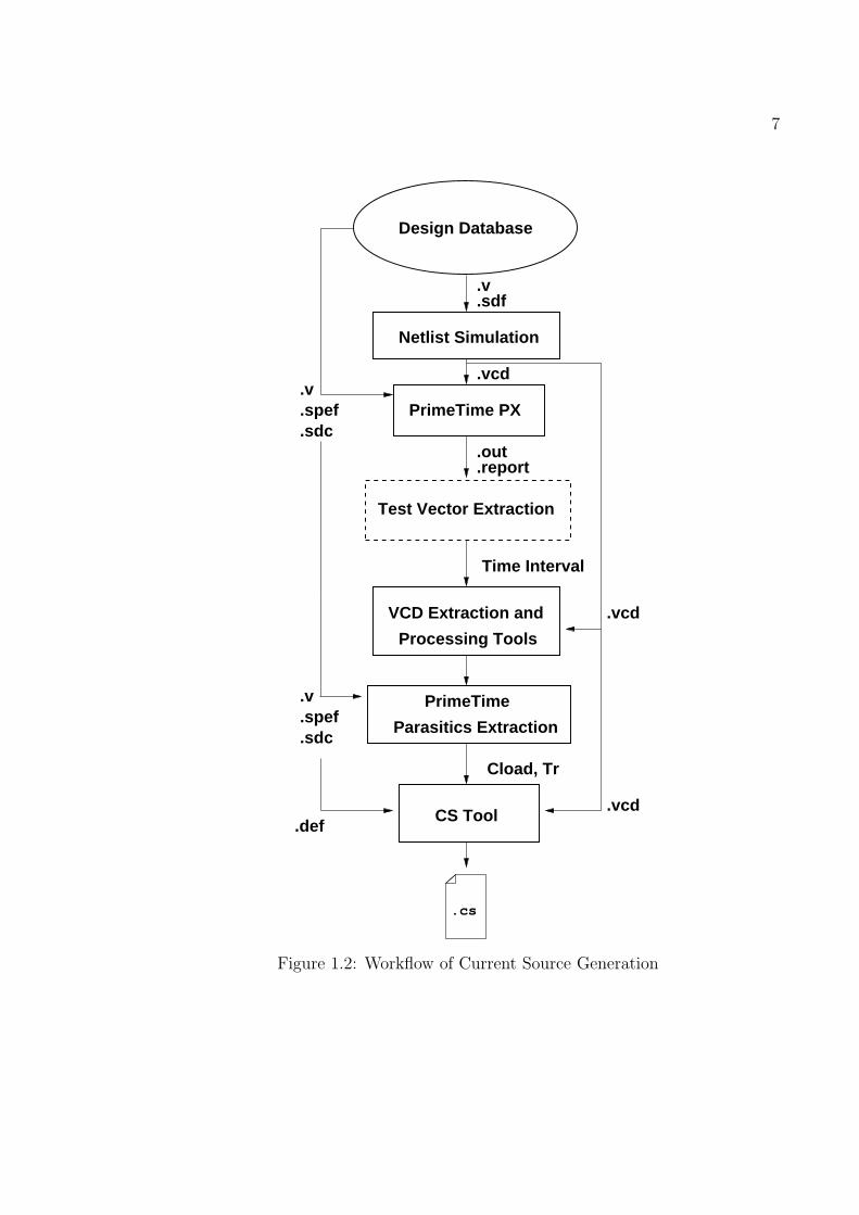
The developments so far are summarized in figure 1.2. Here, intermediate input/outputfiles are stated to increase understanding. From the figure, the “Processing Tools”and “CS Tool” are in-house scripts specific for this flow. Special attention will inthe following chapters be given to the dotted box “Test Vector Extraction” and theintermediate .out file.
The resulting .cs file contains, for a certain switching pattern as defined by a partof a VCD file, a list of all switching gates. The gates are represented with theirgeometrical coordinates on the chip as well as their load capacitance and rise time,as described above. Also, all switching of the gates is presented along with theirrespective times.
This step connects the VCD switching information with the power grid model and arealistic switching pattern can be applied to the nodes of the grid to emulate tran-sistors drawing current. The .cs file is then used with the Raphael extracted griddata to put together a SPICE netlist using an in-house scripting flow. This processis explained in great detail in [5].
The next section explains the “Test vector Extraction” step that selects a part of theVCD to use as switching information in the power grid model.
1.3 The Choice of Test Vectors
With a vector based approach, the current waveforms that load the power grid is verymuch a function of how the chip design is used. Early in the design flow, this infor-mation might not be available. In the case of this design, a simulation test case wasavailable. It does not represent a real in-field use case, but it is a realistic applicationwith software running on the CPU of the microcontroller. The duration of this testcase is 460µs. It involves the start-up phase of the microcontroller, as well as theexecution of a software application computing the Fibonacci series.
1.3.1 Test Vector Extraction
Out of the test case, a short time window is chosen to create the current sourceswitching information. In this context, the time window chosen should represent theinput pattern creating the greatest challenge for the power grid, in order to see whatthe largest voltage drop that the chip experiences will be. Choosing this time windowcorresponds to the dotted “Test Vector Extraction” box in figure 1.2, which takes itsinput from the “PrimeTime PX” box above it. PrimeTime PX is a power analysis
7
.cs
Netlist Simulation
.sdf
.v
PrimeTime PX
.vcd
Test Vector Extraction
Time Interval
VCD Extraction and
Processing Tools
PrimeTime
Parasitics Extraction
Cload, Tr
.def
.v
.spef
.sdc
.vcd
.vcd
Design Database
.out
.report
.spef
.sdc
.v
CS Tool
Figure 1.2: Workflow of Current Source Generation

8
Figure 1.3: The powergrid model in two layers
tool from Synopsys [9].
In previous work using this grid model ([1]), the test vector extraction has been basedon PrimeTime PX’s top power consuming clock cycle from its detailed report. Thisapproach is a common method for selecting a vector and has been used in other stud-ies on IR drop, as mentioned in [10] which argues the method is non-optimal in termsof worst-case voltage drop. This master’s thesis deals with replacing the dotted boxand investigating the power grid using test vectors extracted with a new methodology,which as we shall see is based on the intermediate .out file from figure 1.2.
PrimeTime PX supports both average and time-based power analysis. In the work ofthis thesis, the time-based power analysis has been used. By providing a gate-levelVCD file containing all switching activity of a certain run trace, detailed power dis-sipation data of every part of the chip is reported. Power consumption is calculatedover intervals of time as specified by the user. For example, a 5 ns time interval poweranalysis sums all energy consumed over the 5 ns period and divides by that time toget the power dissipation.
Other than reporting power dissipation of different parts of the chip, PrimeTime PXcan be made to produce power dissipation waveforms. These waveforms specify powerdissipation for every instance of time, defined as above. The waveforms contain powerinformation either for all hierarchical levels except leaf cells, or for all hierarchical lev-els including leaf cells. That is, they contain not only the total chip power dissipationper time unit, but power dissipation per time unit for each cell. With the leaf cell

9
option, the number of power waveforms becomes extremely large. On the other hand,the leaf cell option enables fine-grained monitoring of power consumption and createsa direct mapping between power consumption and cell instances defined in the DEFfile of the design.
1.3.2 The PrimeTime PX Power Trace Waveform file
The power waveforms from PrimeTime PX can be given as either a binary FSDB file,or a text-based .OUT file. Both formats can be used to graphically view the resultsin waveform viewers, but the text-based .OUT format is easier to use for extractinginformation to be post-processed using other applications.
The power waveform .out file format is exemplified below. First, all cell instances inthe design are listed with instance name and an instance number given by PrimeTime.
.index Pc(INSTANCENAME) 4532 Pc
.index PC(HIERARCHICAL/INSTANCENAME) 3211 Pc
Including leaf cells, the number of cell instances with index numbers were for thisdesign over 400 000. Next, for every time instance, the time is followed by all cell in-stance numbers switching during that time interval, along with the power it consumesfor that time.
1
342 1.401e-06
721 3.130e-05
2
523 4.232e-04
211 2.144e-03
For each time instance, there can be a huge number of cells listed with power in-formation. The interval between time instances is the time interval defined by theuser at the start of the analysis and is repeated in the header lines of the .out file.(.time resolution 0.1).
The next chapter will describe the methodology developed in this master’s thesiswhich starts with parsing the PrimeTime PX .out file.

10
1.4 Results of Previous Research
The work-flow of the power grid model used in this thesis has previously been usedin the Atmel/Chalmers research collaboration, where several publications have beenmade based on variations of the model.
In [1], supply voltage drops were studied and the importance of on-chip inductancewas investigated. Here, the test vector which has the highest chip-wide power dissi-pation over one clock cycle is used as stimulus. The article concludes that on-chip selfinductance can have a significant impact on voltage drop, while the effects of mutualinductance remain inconclusive.
Derating of timing margins is the focus of [4]. The same setup as above is used. Thearticle claims derating could be decreased, since voltage drops found are too small tonecessitate the standard 10% supply voltage derating. Note that also in this article,the worst-case test vector was assumed to be the most power consuming clock cycle.
A different power grid extracted in the same work-flow was investigated in [2] and [3].Here, different variables of power grid design were analyzed with the conclusion thatsupply rail width is the most important design variable. In this approach, all currentsources were switching simultaneously instead of extracting switching patterns fromVCD.
Chapter 2
Methods for Test VectorExtraction
The goal of this master’s thesis is to find the test vector out of a large VCD tracethat results in the largest possible voltage drop in the modeled power grid. To selectone 200 MHz clock cycle out of a 460µs long trace, a choice among approximately 92000 possible cycles must be made. Performing SPICE-level simulations on each of thepossible choices is infeasible, so some method is needed to locate the most interestingcycle among the thousands of alternatives.
One initial consideration when cutting out a part of a VCD trace, is the length ofthe time windows chosen. Too large time windows lead to slow processing times forgenerating SPICE netlists, and also long SPICE simulation runtimes. If the timewindow is too short, we might miss some interesting behavior in the switching ac-tivity. In the results presented in this thesis, the time window was chosen to be 200 ns.
Starting with a detailed power simulation of the entire trace, one can begin to makequalified guesses at which cycles would generate the largest voltage drop. One suchguess could be made by assuming that the cycle which consumes the most power ofall the cycles in the trace is the one causing the largest voltage drop. This is readilyavailable from the information in the power simulation, and has commonly been usedas a metric for finding the worst vector ([1], [10]).
However, this qualified guess would not necessarily give the largest voltage drop,as was shown in [10]. In this section, several different methods of making qualifiedguesses of cycles that give large voltage drop will be presented. The different methodsall rely on power information as given by PrimeTime PX, but differ in the way thepower information has been gathered and how the information is analyzed.
11

12
2.1 Power Analysis in PrimeTime PX
A pre-processing flow has been developed by the author to analyze the PrimeTimePX power waveform. Because of the large amounts of data in the waveform file, aswas described in the previous chapter, parsing the file can be quite time consumingif care is not taken. In fact, the .out files for this particular design and simulationtrace can be over 8 GB in a gzipped (compressed) format.
To cope with the large amounts of data and create a good balance of performanceand flexibility, a combination of C, Python and UNIX shell scripts has been used.The method and the resulting data produced will be described in this section.
2.1.1 Total Power Analysis
To analyze power dissipation of the entire chip over time, the power trace waveformscan be used. Waveform viewers can read the file directly, but to work with the datain a more flexible way, some preprocessing is necessary.
In the total chip power context, four items of information was initially of interest:1: Time-Power data,2: Time-dP/dt data,3: Top 100 Power values,4: Top 100 dP/dt values.
This means that for each instance of time, the total chip power dissipation must becalculated. Also, the running differential between two adjacent time instances wascalculated to find possible dP/dt peaks. In the same processing step, top-lists ofpower and dP/dt was maintained by the program. The program was implementedin C, using UNIX tools cat and zcat to pipe data from the huge .out files in eithera gzipped or uncompressed format. A shell script was used to manage analyses ofdifferent waveform files in different time resolutions and to order the output appro-priately in the file system.
The time resolutions of the power analysis and power waveforms from PrimeTimePX, as mentioned in section 1.3.2, is an important consideration. We will see lateron that it can affect the choice of test vectors. The time resolution can be adjustedby the user, but waveform files grow quickly with increased resolution as summarizedin table 2.1. The file sizes are given in gzipped format, the leaf option correspondsto including the leaf cells of the design in the power waveform. With leaf, resolutionsabove 0.1 ns were neglected due to the large file sizes.

13
Resolution File size (leaf) File size (no leaf)5 ns 3.5 GB 445 MB1 ns 5.9 GB 825 MB
0.1 ns 7.4 GB 1.3 GB0.01 ns - 2.5 GB0.001 ns - 4.2 GB
Table 2.1: File size for waveform files by resolution
2.1.2 Extracting Local Power Trace Information
As we shall discuss later, it is sometimes useful to get a power trace of a subsetof the full chip. The PrimeTime PX trace contains (Time:Instance Number:Power)tuples and can be used for this purpose. A specification of localities more coarse-grained than cell instances is usually wanted, and thus an intermediate conversionstep is needed. To this end, a Python script has been developed, that takes a listof nodes (as defined in section 1.2.2) and produces a (longer) list of instance numbers.
Each .out file contains a list of (Instance Number → Instance Name) mappings (re-fer to the example in section 1.3.2). This list is the same for all power analyses ofthe same chip design. For each design, a DEF file containing (Instance Name →X-Y Coordinates) mappings is usually available. Since these mappings never changewithin the same design, performance is increased by only performing the translation(Instance Number→ X-Y Coordinates) once. Python has a programming constructcalled Pickles that is useful for this. A binary file is saved as output from the trans-lation, which is implemented as a hash table that can be quickly indexed to find themapping.
To realize the (Node → Instance Numbers) mapping we need a rule that tells whichinstances should belong to which node. In the flow of section 1.2.2, each gate islumped to the node closest to its coordinates. The same approach is used here: Foreach node stated with x-y-coordinates, list all instances which has that node as itsclosest node (by using the Instance Number→ X-Y Coordinates mapping from above).
This procedure gives us the more coarse-grained locality we are after. Taking thepickle approach one step further, the results of the above will be pickled since it doesnot change within a design. We now have, for each node, a list of all the unit numbers(as defined by PrimeTime PX) belonging to that node.
The relation between units and nodes is illustrated in figure 2.1. Cell is used inter-

14
changeably with unit in this thesis.
unit=5390
unit=94328unit=2175
unit=2774
unit=8974
node=53
Figure 2.1: Illustrating the relationship between units and nodes
The found mapping of (Instance Number → Node) is now combined with the C pro-gram used for extracting power data from the waveform files. A list of nodes is givento the Python program that produces a list of instances. The list of instances is thengiven as input to the C program, that will then create the four items of interest statedin section 2.1.1, but only for those instances belonging to that subset of nodes.
This gives us a general approach for extracting power data for any part, large orsmall, of the chip. This ability will be useful in finding a worst-case vector, as will beexplained in the next section.
2.2 Spatial Locality
When a test vector has been extracted and a SPICE simulation has been performedusing switching data of that test vector, the end result is voltage drop waveforms forall nodes in the power grid. Also, current profiles for all current sources loading thepower grid are available.
It would seem reasonable that a large current drawn in a power grid node wouldalways result in a large voltage drop in that node. To some extent this is true, butresults obtained in this thesis show that there is no absolute one-to-one mapping be-tween current and voltage drop. This section will investigate this relationship, whileintroducing spatial locality of currents and how it can be used for test vector extrac-tion.
To investigate the property of spatial locality, experiments involving 47 test vectorswere performed. Each test vector’s maximum drop was noted along with the nodewhere the drop occurred. For each vector, current profiles for the worst node and forthe nodes directly adjacent to the worst node was loaded. The concept of adjacent

15
nodes is illustrated in figure 2.2. In the figure, the middle node is the node withthe observed maximum voltage drop. Current sources with filled lines indicate thecurrents sources considered for the two cases. Node current means the current drawnby the current source in the node with the maximum voltage drop. Adjacent nodescurrent mean the superimposed currents of the two nodes directly adjacent to thenode with the maximum voltage drop.
(a) Node current (b) Adjacent nodes current
Figure 2.2: Illustrating nodes and adjacent nodes
The goal of the experiment was to see how great the correlation between a node’scurrent consumption and its voltage drop was. Furthermore, the experiment investi-gates the correlation between adjacent nodes’ current and the worst drop.
Other current properties that was explored was maximum dI/dt and maximum totalpower spectral density over frequencies from 0 Hz - 200 MHz.
For each of these properties, the correlation coefficient was calculated. The correlationcoefficient is defined as
R(i, j) =C(i, j)
√
C(i, i)C(j, j)(2.1)
where C(i, j) is the covariance of vectors i and j. The correlation coefficient is astandardized version of covariance that describe the way i and j influence each other[11]. A correlation coefficient of 0 means the two variables are uncorrelated, whileclose to 1 indicates a strong correlation.
Table 2.2 summarizes the correlation coefficients of different current properties to
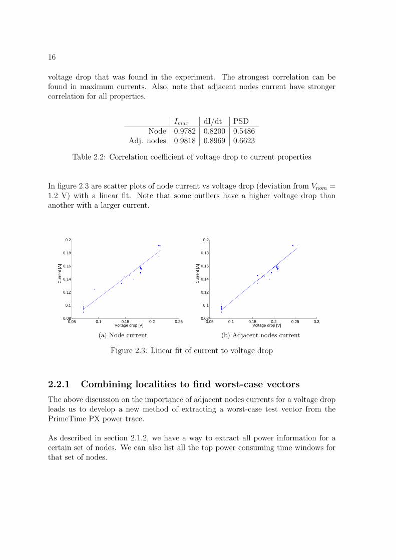
16
voltage drop that was found in the experiment. The strongest correlation can befound in maximum currents. Also, note that adjacent nodes current have strongercorrelation for all properties.
Imax dI/dt PSDNode 0.9782 0.8200 0.5486
Adj. nodes 0.9818 0.8969 0.6623
Table 2.2: Correlation coefficient of voltage drop to current properties
In figure 2.3 are scatter plots of node current vs voltage drop (deviation from Vnom =1.2 V) with a linear fit. Note that some outliers have a higher voltage drop thananother with a larger current.
Cur
rent
[A]
Voltage drop [V]0.05 0.1 0.15 0.2 0.25
0.08
0.1
0.12
0.14
0.16
0.18
0.2
(a) Node current
Cur
rent
[A]
Voltage drop [V]0.05 0.1 0.15 0.2 0.25 0.3
0.08
0.1
0.12
0.14
0.16
0.18
0.2
(b) Adjacent nodes current
Figure 2.3: Linear fit of current to voltage drop
2.2.1 Combining localities to find worst-case vectors
The above discussion on the importance of adjacent nodes currents for a voltage dropleads us to develop a new method of extracting a worst-case test vector from thePrimeTime PX power trace.
As described in section 2.1.2, we have a way to extract all power information for acertain set of nodes. We can also list all the top power consuming time windows forthat set of nodes.

17
Using the extracted power information and list of top power consuming time windowsfor a node which we somehow know to be critical, we can find the time window wherethat node dissipates the largest amount of power over a certain time interval.
Secondly, we can do the same for that node’s adjacent nodes to get the time windowwhere those nodes’ superposed power dissipation reach a maximum.
Thirdly, a larger area of nodes surrounding the critical node can be decided upon.Here, the area holding the CPU of the chip has been decided as a larger localizationof interest. The power dissipation of nodes making up the CPU is thus extracted andthe maximum time window is found.
Now, since from table 2.2 both the critical node and its adjacent nodes’ current cor-relate to the voltage drop, a combined approach is of interest. Using a programmaticapproach, the power dissipation top lists of the critical node and the adjacent nodesare compared for overlaps in time. That is, if the maximum power dissipating cycleof the critical node occurs at the same time as its adjacent nodes, that cycle shouldbe very interesting in terms of worst-case voltage drop. If the maximum two doesnot overlap, perhaps some other of the 100 time windows in the two lists overlap. Toincrease yield, a time window of 100 ns is defined in which any overlaps are consideredto be simultaneous.
The overlap concept is illustrated in figure 2.4. The figures in the left indicate twotop-list entries which are not overlapping. To the right, there is an overlap. The listindex represents the order of significance in the top-100 list. Thus, two overlappingtime windows of index 100 would be given more attention than numbers of 10 and20. This way, the sum of indices give a total ordering of the time windows.
The three levels of localization presented above was combined in the overlap method-ology to successfully identify test vectors with large voltage drop. The results arepresented in the next chapter.

18
t
t
t
t
100 ns
5050
75
List index
List index
List index
List index
100 ns
75
Figure 2.4: Overlapping top-list entries 100ns List index
2.2.2 Finding Worst Node on Chip
The above experiments were performed on vectors more or less randomly selected,and certain nodes were frequently more prone to have large IR drop.
Without any prior knowledge of our design and without results from earlier voltagedrop simulations, can we find out which node will cause the largest IR drop fromlooking at the PrimeTime PX power trace?
To investigate this, an experiment was conducted where each node’s maximum powerdissipation per time unit is found. Using a PrimeTime PX power trace, the stepsoutlined in Algorithm 1 yields every node’s maximum by adding, for every unit thatis dissipating power in a time unit, each node’s power dissipation to the correspondingnode’s sum. A maximum is updated and the sum is reset.

19
Algorithm 1 Finding the maximum power dissipating node
for t = 1 ... endtime dofor Unit ∈ P (t) doNode ← getClosestNode(Unit)Psum(Node) ← Psum(Node) + P (t, Unit)Ptot(Node) ← Ptot(Node) + P (t, Unit)
for Node ∈ all nodes doif Psum(Node)> Pmax(Node) thenPmax(Node)← Psum(Node)
Psum(Node)← 0
This procedure yields two node metrics for each node: 1) The node’s maximum powerdissipation over a time unit and 2) The node’s total power dissipation over the entireVCD duration.
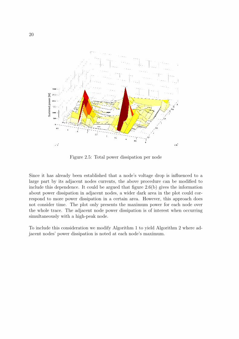
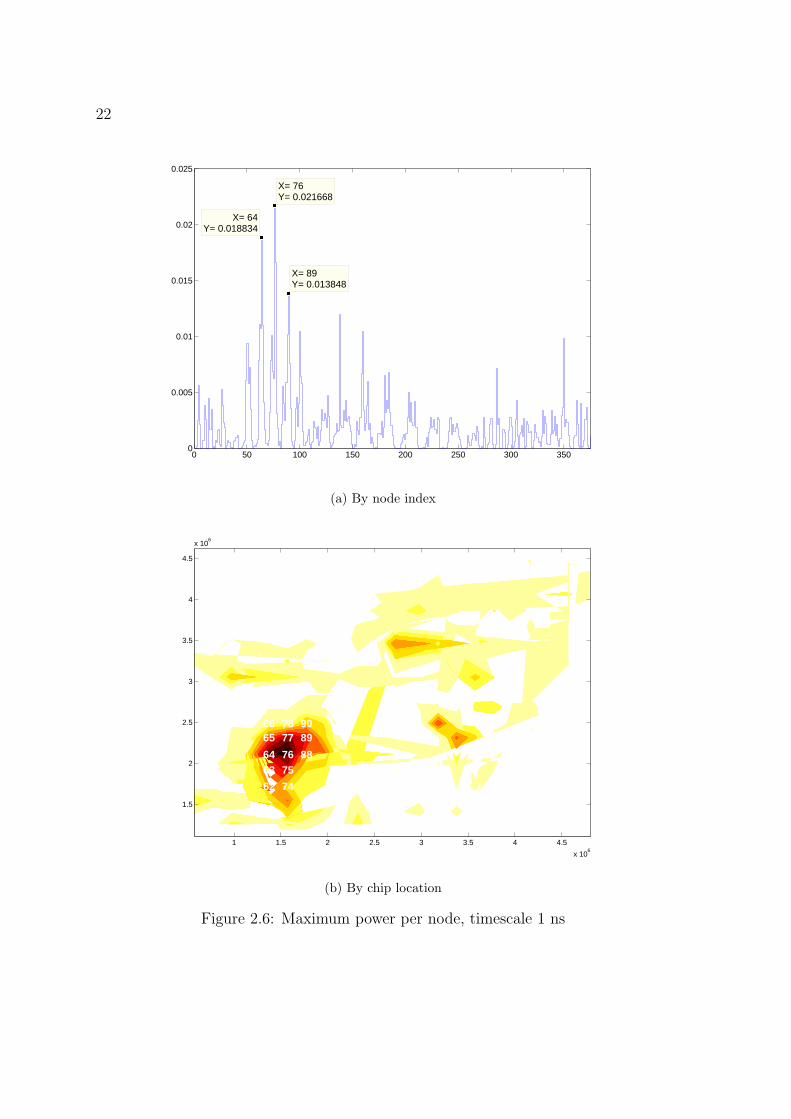
Figure 2.5 shows a 3D-plot of the total power dissipation. It tells us of one specificnode with high total power dissipation. It coincides with the clock tree root andthe high total is explained by noting that this area dissipates power for each clockcycle. The second most noticeable area coincides with the CPU. However, we areparticularly interested in instantaneous maximums rather than how often a certainnode dissipates power. Thus, figure 2.6 is of particular interest. Figure 2.6 displayeach node’s maximum in a time instance. In (a), the maximum is plotted by node in-dex. In (b), the nodes are displayed with the geometrical location on the chip, wheredarker areas mean more power. The annotated numbers correspond to the x-axis offigures 2.6(a).
20
Sum
med
pow
er [W
]
Figure 2.5: Total power dissipation per node
Since it has already been established that a node’s voltage drop is influenced to alarge part by its adjacent nodes currents, the above procedure can be modified toinclude this dependence. It could be argued that figure 2.6(b) gives the informationabout power dissipation in adjacent nodes, a wider dark area in the plot could cor-respond to more power dissipation in a certain area. However, this approach doesnot consider time. The plot only presents the maximum power for each node overthe whole trace. The adjacent node power dissipation is of interest when occurringsimultaneously with a high-peak node.
To include this consideration we modify Algorithm 1 to yield Algorithm 2 where ad-jacent nodes’ power dissipation is noted at each node’s maximum.

21
Algorithm 2 Finding the maximum power dissipating node, including adjacentnodes
for t = 1 ... endtime dofor Unit ∈ P (t) doNode ← getClosestNode(Unit)Psum(Node) ← Psum(Node) + P (t, Unit)Ptot(Node) ← Ptot(Node) + P (t, Unit)
for Node ∈ all nodes doif Psum(Node)> Pmax(Node) thenPmax(Node)← Psum(Node)Padjacent(Node)← Psum(Node−1) +Psum(Node+1)
Psum(Node)← 0
which yields a list of each node’s maximum current, and its adjacent nodes’ currentat that time instance. To find the node that should experience the worst-case voltagedrop according the this criterion is thus found by finding the node with maximumcombined node/adjacent node power.
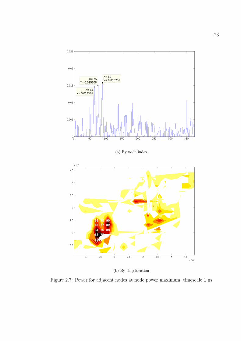
Figure 2.7 shows, for each node, its adjacent nodes’ power at the instance of timewhere the node has its maximum.
Some interesting observations can be made regarding these figures. First, the areas ofmaximum power roughly make up the area of the CPU. Secondly, while node number76 is the most power consuming node, its adjacent nodes in that time instance isnot as prominent. Considering nodes/adjacent nodes, the focus has shifted to nodenumber 63/64 and node 89.
22
0 50 100 150 200 250 300 3500
0.005
0.01
0.015
0.02
0.025
X= 89Y= 0.013848
X= 76Y= 0.021668
X= 64Y= 0.018834
(a) By node index
76
77 89
88
9065
6463
62
66 78
75
74
1 1.5 2 2.5 3 3.5 4 4.5
x 106
1.5
2
2.5
3
3.5
4
4.5
x 106
(b) By chip location
Figure 2.6: Maximum power per node, timescale 1 ns
23
0 50 100 150 200 250 300 3500
0.005
0.01
0.015
0.02
0.025
X= 75Y= 0.015108
X= 64Y= 0.014562
X= 89Y= 0.015751
(a) By node index
7576
77 89
88
9065
6463
62
66 78
1 1.5 2 2.5 3 3.5 4 4.5
x 106
1.5
2
2.5
3
3.5
4
4.5
x 106
(b) By chip location
Figure 2.7: Power for adjacent nodes at node power maximum, timescale 1 ns

24
Thus, three nodes in particular attract our interest. Node 63, node 76 and node 89.But which characteristic of power dissipation is the most important? Will a lonelynode with large maximum power dissipation cause the larger drop or will a node withrelatively large power dissipation surrounded by other power dissipating nodes beworse?
For all found node maximums, the time instance will be presented along with themaximum by using the method outlined above. Thus, we can easily make test vec-tors from the interesting cases and evaluate the voltage drops by runnings SPICEsimulations (results follow in the next chapter).
Changing the Time Resolution
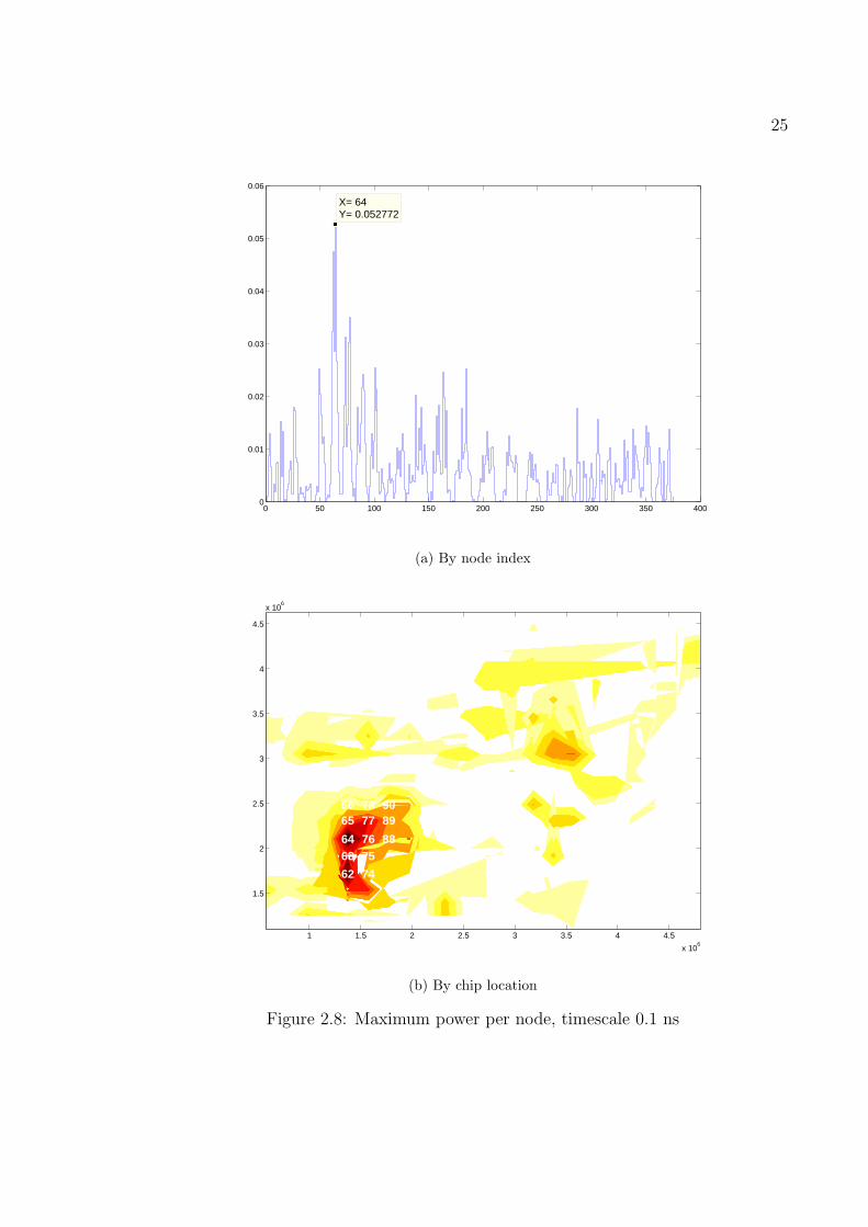
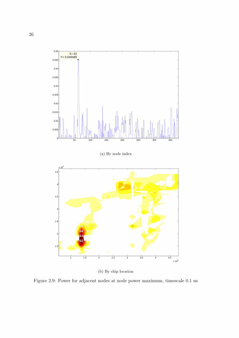
As it was noted in section 3.1, it is important to select a proper time resolution whenperforming peak power analysis. The above experiments were repeated with the timeresolution 0.1 ns, which yielded different results.
Figure 2.8 shows each node’s maximum power dissipation over 0.1 ns, by node index(a) and by chip location (b). Compared to figure 2.6, focus has shifted from node 76to node 62. Node 64 is the other node of particular interest, from figure 2.8(a) wenote that it is the maximum power dissipating node.
In figure 2.9, the summed power of adjacent nodes for each node is plotted. Here, node62 is the maximum. That means that node 62 is the node which, at its maximum 0.1ns power interval, has the greatest power consuming adjacent nodes. Given the earlierdiscussion about the importance of adjacent nodes power dissipations, we could ex-pect node 62 to experience a large voltage drop at the time when this scenario occurs.
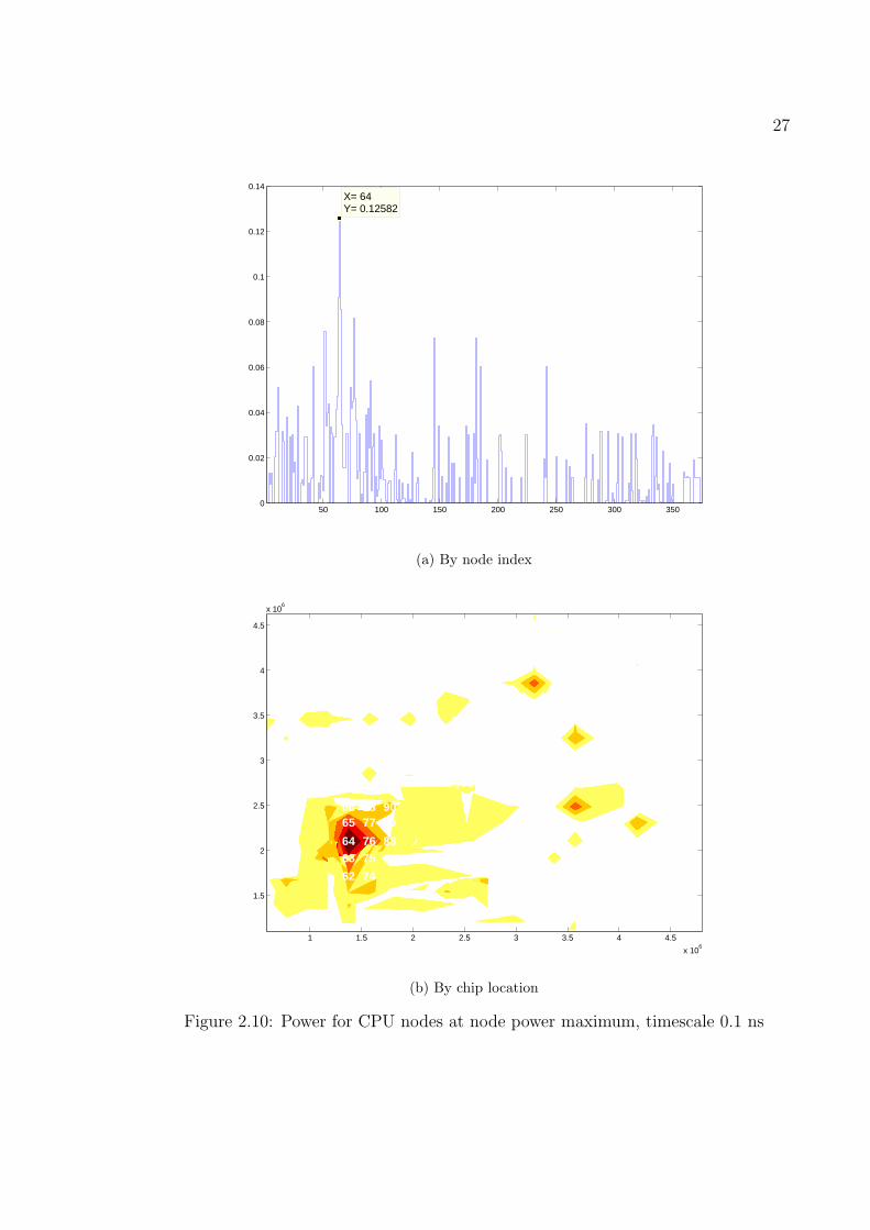
The next figure (2.10) extends the locality concept. Here, for each node, the totalpower dissipation of the CPU area at the time of node power maximum, is presented.In this setting, node 64 is dominating. This means that node 64 is the node that hasits maximum power dissipation at the time instance when the CPU dissipates themost power for any node’s power maximum. This time instance should be partic-ularly interesting, because node 64 was the top power consuming node (figure 2.8),and peaked when the surrounding CPU nodes were particularly active.
25
0 50 100 150 200 250 300 350 4000
0.01
0.02
0.03
0.04
0.05
0.06
X= 64Y= 0.052772
(a) By node index
76
77 89
88
9065
6463
62
66 78
75
74
1 1.5 2 2.5 3 3.5 4 4.5
x 106
1.5
2
2.5
3
3.5
4
4.5
x 106
(b) By chip location
Figure 2.8: Maximum power per node, timescale 0.1 ns
26
50 100 150 200 250 300 3500
0.005
0.01
0.015
0.02
0.025
0.03
0.035
0.04
0.045
0.05X= 62
Y= 0.045085
(a) By node index
76
77 89
88
9065
6463
62
66 78
75
74
1 1.5 2 2.5 3 3.5 4 4.5
x 106
1.5
2
2.5
3
3.5
4
4.5
x 106
(b) By chip location
Figure 2.9: Power for adjacent nodes at node power maximum, timescale 0.1 ns
27
50 100 150 200 250 300 3500
0.02
0.04
0.06
0.08
0.1
0.12
0.14X= 64Y= 0.12582
(a) By node index
76
77 89
88
9065
6463
62
66 78
75
74
1 1.5 2 2.5 3 3.5 4 4.5
x 106
1.5
2
2.5
3
3.5
4
4.5
x 106
(b) By chip location
Figure 2.10: Power for CPU nodes at node power maximum, timescale 0.1 ns

28
2.3 Frequency Domain
Since a voltage drop is made up of both IR-drop (caused by parasitic resistance inthe power grid) and L dI/dt drop (caused by parasitic inductance in the power grid),where L dI/dt can constitute a significant contribution [1], we will investigate howthe frequency dependence of the power grid relates to the voltage drop.
It is customary to characterize a circuit and power delivery system by its frequencyresponse using an impedance plot. An impedance plot gives the system’s impedancefor all frequencies of interest. For a characterization of the complete power deliverysystem, the power supply and voltage regulators along with the PCB, die-packaging,bond-wires and on-chip power grid should be considered.
Impedance plots can be used to discover resonant frequencies in the power grid. Res-onance in an electric circuit can cause energy to oscillate back and forth betweenmagnetic energy in an inductance to electric energy in a capacitance. Another way toview the problem is to consider the impedance of a resistor and an inductor in seriesconnection, Z = R + jωL. This impedance increases with frequencies so that fastedge-rates would become problematic. Using bypass capacitors in parallel createsan impedance of Z = 1
jωC+ R + jωL, which has its minimum at its self-resonant
frequency fresonant =ωresonant
2π= 1
2π√
LC[12].
The bypass capacitor approach can thus be used to lower impedance over any rangeof frequencies necessary. However, several bypass capacitors in parallel can cause an-other phenomenon called antiresonance [6], which at specific frequencies can increaseimpedance dramatically (the term antiresonance describes the phenomenon more ac-curately, but this thesis will use the term resonance to refer to the above, unwanted,behavior). It is therefore important to carefully design the power delivery systemand control the type and amount of added decoupling capacitance to keep systemimpedance low over the frequency range of chip operation. Note that the frequencyrange here includes all frequency components of switching times of on-chip signals,and not only the clock frequency.
From the above discussion, we can apply the concept of (anti) resonant frequen-cies to the search for test vectors causing voltage drop. If we were to find certainswitching patterns with large components near resonant peaks, this could lead tohigh impedance and thus high voltage drop in the circuit. Some earlier research hasfocused on this subject. In [10], the authors claim to find worst-case vectors based onresonant frequencies rather than maximum power dissipation. Their work is based onFFT techniques. In [13], wavelets are used to create worst-case currents containingfrequencies coinciding with the impedance peaks of the power delivery systems.
29
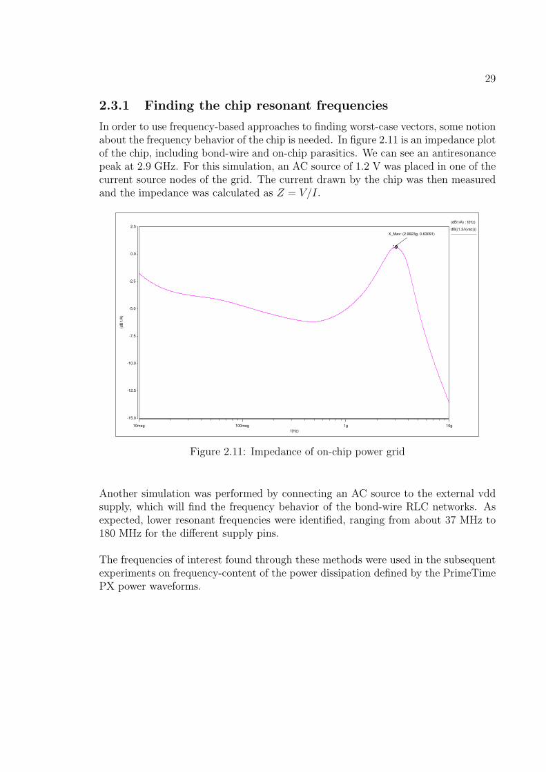
2.3.1 Finding the chip resonant frequencies
In order to use frequency-based approaches to finding worst-case vectors, some notionabout the frequency behavior of the chip is needed. In figure 2.11 is an impedance plotof the chip, including bond-wire and on-chip parasitics. We can see an antiresonancepeak at 2.9 GHz. For this simulation, an AC source of 1.2 V was placed in one of thecurrent source nodes of the grid. The current drawn by the chip was then measuredand the impedance was calculated as Z = V/I.
f(Hz)
10meg 100meg 1g 10g
(dB
1/A
)
−15.0
−12.5
−10.0
−7.5
−5.0
−2.5
0.0
2.5
X_Max: (2.9923g, 0.63091)
(dB1/A) : f(Hz)
dB((1.2/i(vac)))
Figure 2.11: Impedance of on-chip power grid
Another simulation was performed by connecting an AC source to the external vddsupply, which will find the frequency behavior of the bond-wire RLC networks. Asexpected, lower resonant frequencies were identified, ranging from about 37 MHz to180 MHz for the different supply pins.
The frequencies of interest found through these methods were used in the subsequentexperiments on frequency-content of the power dissipation defined by the PrimeTimePX power waveforms.
30
2.3.2 FFT based approaches
The FFT (Fast Fourier Transform) based approach was influenced by the work donein [10], where a worst-case test vector from a large VCD trace is found by looking forthe time window with the largest frequency components close to the chip resonancefrequency.
In this thesis, the frequency-based worst-case was found in the following way. Start-ing with a full-chip PrimeTime PX power trace, the power data was broken downinto time windows. A time window was defined to be 100 ns. For each time window,the power spectral density was calculated using FFT. The time window was thenmoved 10 ns forward in time to produce a new time window. For each time win-dow, the summed power spectral density was calculated over a range of frequencies,[fcenter −
f∆2, ..., fcenter +
f∆2], where fcenter is the interesting resonance frequency and
f∆ defines a tolerance range of nearby frequencies.
The time at which each interesting frequency has its maximum was noted and laterused to extract a test vector from the VCD trace.
2.3.3 Wavelet based approaches
Wavelet transforms are mathematical transformations that can be used to combinethe frequency-domain information of the Fourier transform with time-domain infor-mation of the signal. They have been used in many applications of signal processing,such as climate research, medical analysis, financial analysis and image de-noisingand compression [14].
In the context of power integrity analysis in VLSI, a few research papers have beenwritten that utilize the wavelet transforms ([13] [15]). In [13], the time-frequencyproperties of the wavelet transforms are used to construct a worst-case current stim-ulus depending on the system’s frequency behavior. Processor architectural powersimulations are targeted in [15] to predict how large the power ripple will be for agiven benchmark.
In the work of this thesis, the wavelet approach and the idea of combining the timeand frequency domain was combined with the ideas of [10] to extract parts of a largeVCD trace with interesting frequency components.
Using Matlab and the Signal Processing Toolbox, the Continuous Wavelet Transform(CWT) of a PrimeTime PX power trace was calculated. The CWT divides the sig-nals frequencies in a number of scales. The scales represent frequencies according tosome mapping. For each instance of time, the magnitude of each scale is calculated.
31
This means we can get information about when in time certain frequency compo-nents exist. This is interesting when we are considering a long power trace and lookfor certain frequencies. We can immediately find the time instance where a certainfrequency of interest is large.
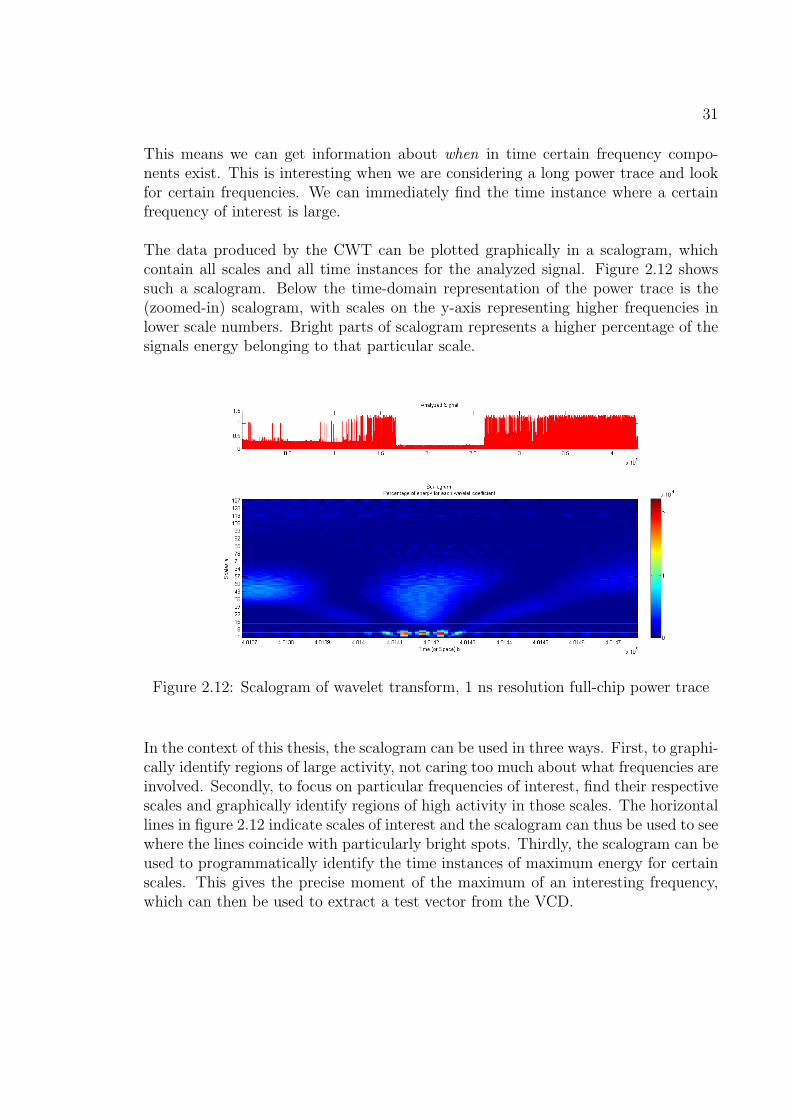
The data produced by the CWT can be plotted graphically in a scalogram, whichcontain all scales and all time instances for the analyzed signal. Figure 2.12 showssuch a scalogram. Below the time-domain representation of the power trace is the(zoomed-in) scalogram, with scales on the y-axis representing higher frequencies inlower scale numbers. Bright parts of scalogram represents a higher percentage of thesignals energy belonging to that particular scale.
Figure 2.12: Scalogram of wavelet transform, 1 ns resolution full-chip power trace
In the context of this thesis, the scalogram can be used in three ways. First, to graphi-cally identify regions of large activity, not caring too much about what frequencies areinvolved. Secondly, to focus on particular frequencies of interest, find their respectivescales and graphically identify regions of high activity in those scales. The horizontallines in figure 2.12 indicate scales of interest and the scalogram can thus be used to seewhere the lines coincide with particularly bright spots. Thirdly, the scalogram can beused to programmatically identify the time instances of maximum energy for certainscales. This gives the precise moment of the maximum of an interesting frequency,which can then be used to extract a test vector from the VCD.
32
Several test vectors have been extracted using the wavelet scalogram as a guide. Theirresulting voltage drop will be presented in the next chapter. Some of them were guidedby certain anti-resonant frequencies, while some were identified only by looking at re-gions of large overall activity. In order to capture anti-resonant frequencies identifiedin the on-chip grid, which are of the order of magnitude of a few gigahertz, the waveletapproach presented here could not be used. A fine time-resolution of 0.1 ns or lessneeds to be used to capture the high frequency content, and a high time-resolutionmeans very large amounts of data. This caused the wavelet transform to run veryslowly, and the experiments were abandoned.
It should be noted that the possibilities of using wavelet transforms are far from ex-hausted in this work. For example, the discrete wavelet transform (DWT) was used in[15] but it was not attempted here. Also, the choice of base wavelet used could affectthe outcome. Further experiments with finer time resolutions should also be triedout. The concept of time-frequency information contained in the wavelet transformis suiting for this type of application, and if frequency information would prove to beimportant for the test vector extraction, the wavelet approach should be revisited.
2.4 Cell-level Power Information
Simultaneous switching noise occurs largely due to the synchronous nature of in-tegrated circuits - the clock is designed to arrive more or less simultaneously to allflip-flops within a clock domain. When many flip-flops change state at the same time,large currents are drawn to the flip-flops, in turn causing a quick voltage drop.
This knowledge warranted a further investigation of how different parts of a voltagedrop waveform is made up of different types of cells. Due to naming conventions usedin the design of this chip, the cells specified in a PrimeTime PX power trace couldbe differentiated as flip-flop, clock buffer and combinatorial gates.
For a certain test case, an intermediate step in constructing a current source netlist isto create a file listing all cells that are switching in that test case, along with its loadcapacitance, transition time and the switching times for all transitions. The cells,however, are only specified as X-Y coordinates in this listing, the cell name is notexplicitly stated.
Given a voltage drop waveform for a certain node, we are then interested in breakingdown the cell listing into the types of cells it contains. Furthermore, we want to listthose cells that switch in a certain time interval, say, the time span of the largestspike. Also, since we look at a waveform of a certain node, we want only to see the
33
cells belonging to that node.
The pieces of information needed for such a scheme is 1) cell home-node, 2) cell name,3) transition times.
Each cell’s home-node can be found by using the X-Y coordinates of the switchingfile cell listing and a mapping function designed for other purposes as part of thisthesis work (see section 2.1.2). The cell name can be found in a similar manner, thechip design DEF files contain mappings from cell instance name to X-Y coordinates.The transition times are available in the switching current (.cs) file.
The algorithm for extracting the cell type breakdown is presented as Algorithm 3,and yields information about how many cells of each type switch in a given timeinterval, T .
Algorithm 3 Extract number of cells of each type
for line in cs-file doif Cell ∈ Node thenif Cellswitching ∈ T thencellname← getCellNamecelltype← getCellType(cellname)counter(celltype)← counter(celltype) + 1
2.4.1 Types of Cells Distribution for Test Vectors
Before conducting the above experiments, it was hypothesized how the distributionof cells would look.
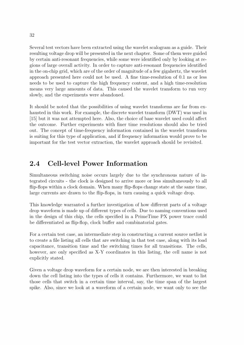
Refer to figure 2.13, where the annotations describe three distinct parts of the wave-form. The first part is drop leading up to before the deep spike. The second part isthe spike. The third and last part is the time after the spike up until the voltage hasrecovered.
34 (
V)
1.12
1.13
1.14
1.15
1.16
1.17
1.18
1.19
1.2
1.21
t(s)
96n 97n 98n 99n 100n 101n 102n 103n 104n
(99.164n, 1.1923)
(99.885n, 1.1424)
(100.19n, 1.188)
Delta X: 709.9p
Delta X: 4.7075n
Delta X: 309.4p
(104.9n, 1.195)
Figure 2.13: Voltage Drop with different components highlighted
This section’s initial reasoning about simultaneous switching noise would lead us tobelieve that the short spike would consist of flip-flops switching. We can also arguethat before the clock reaches its destination flip-flops, a number of clock buffers lead-ing up to the flip-flops should consume power. This interval is the first interval in thefigure. After the switching of the flip-flops, combinatorial logic in between registersswitch to calculate a new circuit state. This would correspond to the final interval.
The results of this analysis confirm the theoretical reasoning, except in this case nocombinatorial logic switched in the post-spike part. In table 2.3 the three voltagedrop parts and their constituent cells are stated.
Cells Flip-Flops Clock-buffersPre-spike 9 0 9
Spike 28 18 0Post-spike 0 0 0
Table 2.3: Switching Cell Types in a Voltage Drop
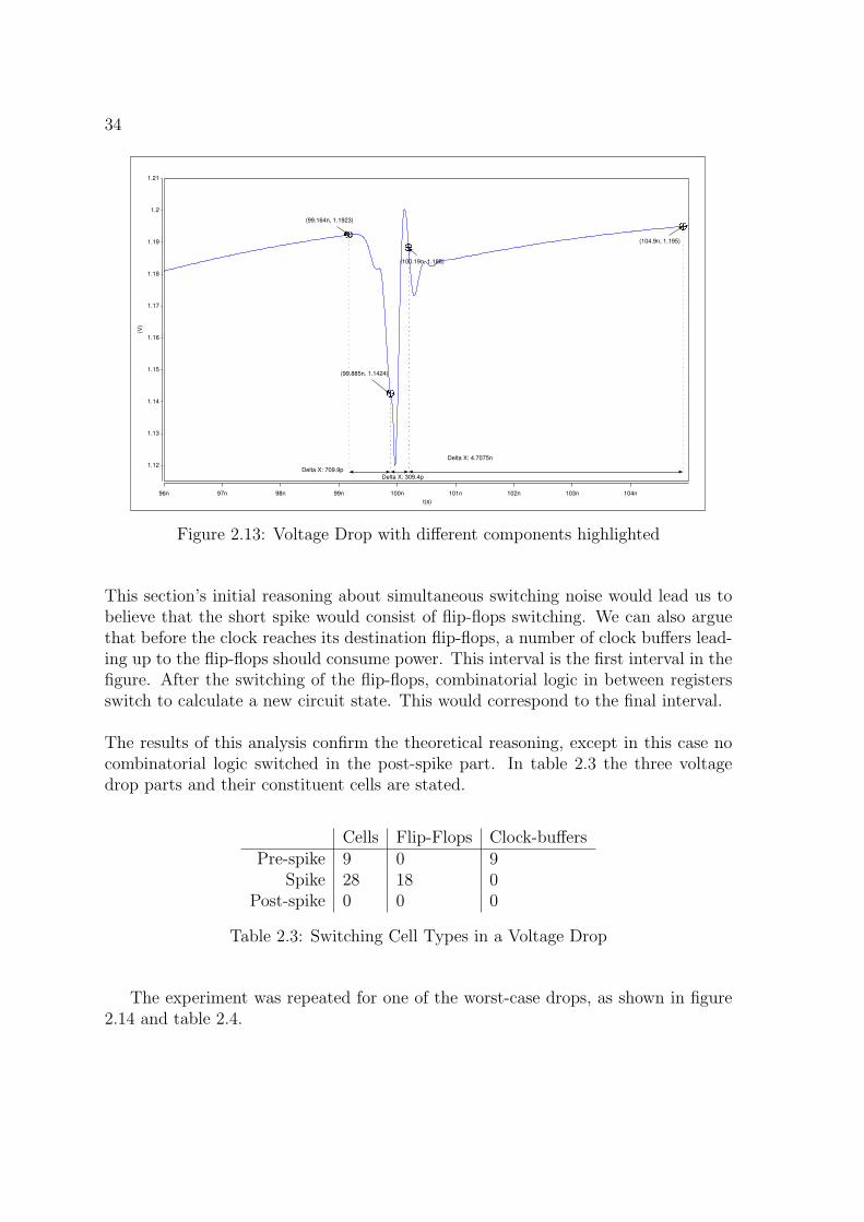
The experiment was repeated for one of the worst-case drops, as shown in figure2.14 and table 2.4.
35
(V
)
0.95
1.0
1.05
1.1
1.15
1.2
1.25
t(s)
30n 32n 34n 36n 38n
(31.309n, 1.0857)
(30.396n, 1.1941) (37.493n, 1.193)
Delta X: 768.57p Delta X: 139.65p
Delta X: 197.84p
Delta X: 5.9773n
(31.17n, 1.0854)
(31.509n, 1.1693)
Figure 2.14: Voltage Drop with different components highlighted, worst-case drop
Cells Flip-Flops Clock-buffersPre-spike 46 28 3
Spike 21 20 0Post-spike 5 5 0
End 11 1 3
Table 2.4: Switching Cell Types in a worst-case Voltage Drop
Confirming the theory and gaining more understanding for the voltage drop wave-forms we are dealing with is a goal in itself. However, an even more interesting resultspawned from this methodology.
The experiment was performed for the reference test vector and for a test vector withan especially large voltage drop, table 2.5 contains the results.

36
Cells Flip-FlopsReference vector 48 1
Large drop vector 148 78
Table 2.5: Switching Cell Types in a Voltage Drop
This indicates that a large number of simultaneously switching flip-flops localized toa single node on the chip gives rise to large voltage drops. A way to search for worst-case test vectors could be to extract the portion of a PrimeTime PX trace only madeup of flip-flops. Pin-pointing the maximum flip-flop intensive clock cycle then lead tovectors causing large voltage drops. This method is not included in this thesis, butis rather left as an area of future work.
2.4.2 Alleviating Simultaneous Switching Noise Through Skew
Spreading
Now, knowing the location of areas that can lead to large voltage drops, and knowingthat a large part of the switching that causes the voltage drop is flip-flops, can thisinformation be used to alleviate the simultaneous switching noise and thus the voltagedrop?
In fact, a fairly common technique for dealing with simultaneous switching noise isto intentionally skew the arrival of clocks to nearby flip-flops, so called useful-skew orskew-spreading. Many research papers have been written on the subject, ([16], [17]and [18] are good examples) and some EDA tools have features to help the backendengineer create a clock skew scheme that lowers IR drop by introducing non-zeroclock skew.
The skew-spreading approach was applied to this model in order to evaluate how a suc-cessful skew-spreading scheme could affect the voltage drop. Since the cell switchinginformation file contains switching times for each switching cell, the above approachof singling out switching registers can be modified to emulate skew-spreading.
Algorithm 3 is then modified as Algorithm 4.

37
Algorithm 4 Extract number of cells of each type
for line in cs-file doif Cell ∈ Node thenif Cellswitching ∈ T thencellname← getCellNamecelltype← getCellType(cellname)if celltype == register thenif cellcount is even thenCellswitching ← Cellswitching + skewvalue
cellcount← cellcount+ 1
This algorithm skews every other register in the time-span/area of interest by a spec-ified amount through adding or subtracting time from the transition time.
Note that this method does not ensure timing-correct functionality of the design.Neither does it ensure any kind of optimal skewing strategy. It is merely a first naivemethod applied to a model of the design to show possible benefits.
However, even a first-guess value (kept within reasonable values of skew spreading)yielded surprisingly good results, which are presented in the results section.

Chapter 3
Results
In the work of this master’s thesis, over one hundred SPICE simulations have beenperformed, with different test vectors used to create the switching patterns loading thepower grid model. The test vectors were found using the different methods presentedin chapter 2. This chapter presents the results of these simulations, focusing on themaximum voltage drops of each test vector extraction methodology.
3.1 Full-chip Maximum Power
In the work preceding this master’s thesis, the time window identified through find-ing the full-chip maximum power calculated over a 5 ns time interval was used as aworst-case test vector.
While this vector was previously considered to exhibit a large drop, its drop is dwarfedalready by vectors found by other naive approaches. For example, the total poweranalysis can be made more detailed by calculating the maximum power over a powertrace of a finer time resolution.
While the reference vector was found by considering a 5 ns resolution power trace, thework in this thesis has also considered resolutions of 1 ns, 0.1 ns, 0.01 ns and 0.001ns. As it was mentioned in section 2.1.1, increased resolution leads to larger file sizes.However, when considering full-chip power, the leaf option was deemed unnecessaryso finer time resolutions could be used.
In table 3.1, the maximum voltage drop of vectors found using the total power anal-ysis approach is summarized along with the times at which the time window for thetest vectors are centered. The maximum voltage drop has gone from 8% of the nomi-nal voltage supply to 13%. This represents a 62% increase in maximum voltage dropestimation only by analyzing power at a marginally finer time resolution.
38

39
Power Trace Resolution (ns) Vmin At Time (ns) Worst node5 1.1034 49228 2031 1.0430 310481 64
0.1 1.0430 356241 640.01 1.0428 382481 640.001 1.0422 190641 64
Table 3.1: Total Power Approach, time resolution Vs maximum voltage drop
The result is easy to reach, yet meaningful for vector-based power integrity analysis:selecting a proper resolution for power calculations is crucial when using a total-powerbased approach.
The importance of time-resolution can also be seen in the following figures (3.1),which plot the full-chip power over the entire time of the VCD trace, in three differ-ent time resolutions. Annotated in the figures are voltage drops for 42 test vectors,which were taken from the part of the figures where they appear. Their location inthe y-axis represent their relative magnitude and shows us that large drops tend to belocated near the end of the trace. Note that in the 5 ns resolution, the activity seenin the later part of the trace is negligible, while all the large drops actually occur here.
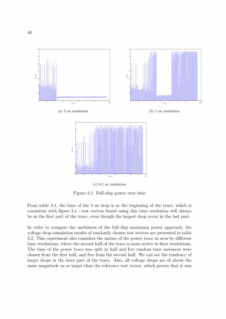
40
Time [ns]
0 0.5 1 1.5 2 2.5 3 3.5 4 4.5
x 105
Pow
er [W
]
0
0.05
0.1
0.15
0.2
0.25
0.3
0.35
(a) 5 ns resolution
Time [ns]
0 0.5 1 1.5 2 2.5 3 3.5 4 4.5
x 105
Pow
er [W
]
0
0.2
0.4
0.6
0.8
1
1.2
1.4
(b) 1 ns resolution
Time [ns]
0 0.5 1 1.5 2 2.5 3 3.5 4 4.5
x 106
Pow
er [W
]
0
1
2
3
4
5
6
7
(c) 0.1 ns resolution
Figure 3.1: Full-chip power over time
From table 3.1, the time of the 5 ns drop is in the beginning of the trace, which isconsistent with figure 3.1 - test vectors found using this time resolution will alwaysbe in the first part of the trace, even though the largest drop occur in the last part.
In order to compare the usefulness of the full-chip maximum power approach, thevoltage drop simulation results of randomly chosen test vectors are presented in table3.2. This experiment also considers the nature of the power trace as seen by differenttime resolutions, where the second half of the trace is more active in finer resolutions.The time of the power trace was split in half and five random time instances werechosen from the first half, and five from the second half. We can see the tendency oflarger drops in the later part of the trace. Also, all voltage drops are of about thesame magnitude as or larger than the reference test vector, which proves that it was

41
not a good way to select a test vector if peak voltage drop was the objective. Anotherthing to note is that some random vectors chosen from the second half of the tracehad as large voltage drop as those found by finer time resolutions of the full-chipmaximum power approach (see table 3.1) - some better method must be used to findvectors that are worse than those selected randomly.
Test Vector Vmin At Time (ns) Worst nodeFirst half, 1 1.1097 96091 203First half, 2 1.1090 23452 203First half, 3 1.1090 61409 203First half, 4 1.1037 49199 203First half, 5 1.1028 90147 203
Second half, 1 1.0435 300490 64Second half, 2 1.0430 362770 64Second half, 3 1.0522 342730 64Second half, 4 1.1018 409920 203Second half, 5 1.0443 388500 64
Table 3.2: Voltage drop of randomly selected test vectors
3.2 Frequency and dP/dt based approaches
The dP/dt approach was motivated by the L dI/dt part of voltage drops. By findingthe fastest power transitions, this could translate to fast current transitions whichwould lead to large voltage drops. These vectors were found at the same time asfull-chip maximum power vectors, as explained in 2.1.1.
The largest dP/dt for different time resolutions along with voltage drops are pre-sented in table 3.3, and do not differ significantly from the full-chip maximum powerapproach.
Time Resolution Vmin At Time (ns) Worst node5 ns 1.1051 79933 2031 ns 1.0429 310482 64
0.1 ns 1.0459 407772 640.01 ns 1.0458 191711 640.001 ns 1.1019 117931 203
Table 3.3: Voltage drop of dP/dt-based vectors
42
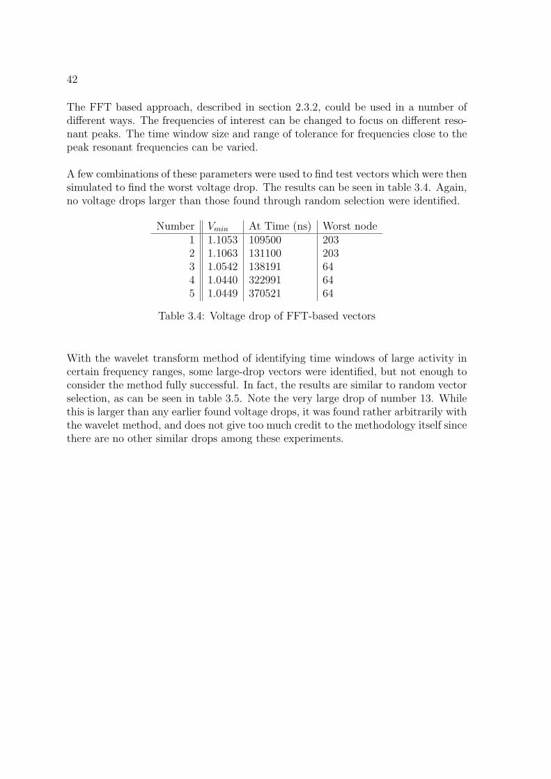
The FFT based approach, described in section 2.3.2, could be used in a number ofdifferent ways. The frequencies of interest can be changed to focus on different reso-nant peaks. The time window size and range of tolerance for frequencies close to thepeak resonant frequencies can be varied.
A few combinations of these parameters were used to find test vectors which were thensimulated to find the worst voltage drop. The results can be seen in table 3.4. Again,no voltage drops larger than those found through random selection were identified.
Number Vmin At Time (ns) Worst node1 1.1053 109500 2032 1.1063 131100 2033 1.0542 138191 644 1.0440 322991 645 1.0449 370521 64
Table 3.4: Voltage drop of FFT-based vectors
With the wavelet transform method of identifying time windows of large activity incertain frequency ranges, some large-drop vectors were identified, but not enough toconsider the method fully successful. In fact, the results are similar to random vectorselection, as can be seen in table 3.5. Note the very large drop of number 13. Whilethis is larger than any earlier found voltage drops, it was found rather arbitrarily withthe wavelet method, and does not give too much credit to the methodology itself sincethere are no other similar drops among these experiments.
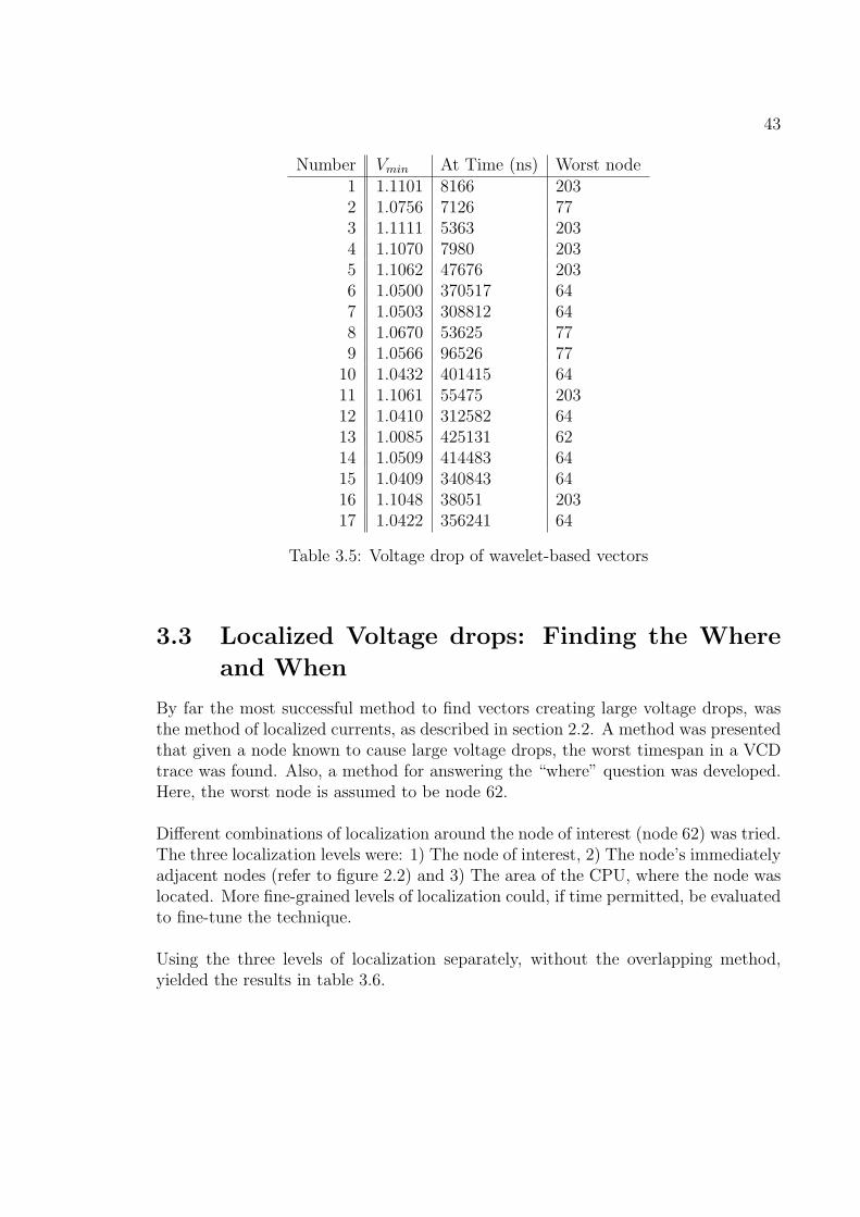
43
Number Vmin At Time (ns) Worst node1 1.1101 8166 2032 1.0756 7126 773 1.1111 5363 2034 1.1070 7980 2035 1.1062 47676 2036 1.0500 370517 647 1.0503 308812 648 1.0670 53625 779 1.0566 96526 7710 1.0432 401415 6411 1.1061 55475 20312 1.0410 312582 6413 1.0085 425131 6214 1.0509 414483 6415 1.0409 340843 6416 1.1048 38051 20317 1.0422 356241 64
Table 3.5: Voltage drop of wavelet-based vectors
3.3 Localized Voltage drops: Finding the Where
and When
By far the most successful method to find vectors creating large voltage drops, wasthe method of localized currents, as described in section 2.2. A method was presentedthat given a node known to cause large voltage drops, the worst timespan in a VCDtrace was found. Also, a method for answering the “where” question was developed.Here, the worst node is assumed to be node 62.
Different combinations of localization around the node of interest (node 62) was tried.The three localization levels were: 1) The node of interest, 2) The node’s immediatelyadjacent nodes (refer to figure 2.2) and 3) The area of the CPU, where the node waslocated. More fine-grained levels of localization could, if time permitted, be evaluatedto fine-tune the technique.
Using the three levels of localization separately, without the overlapping method,yielded the results in table 3.6.
44
Locality Vmin Worst nodeCPU 1.0441 64Node 1.0251 62
Adj. Nodes 1.0546 64
Table 3.6: Localized power results
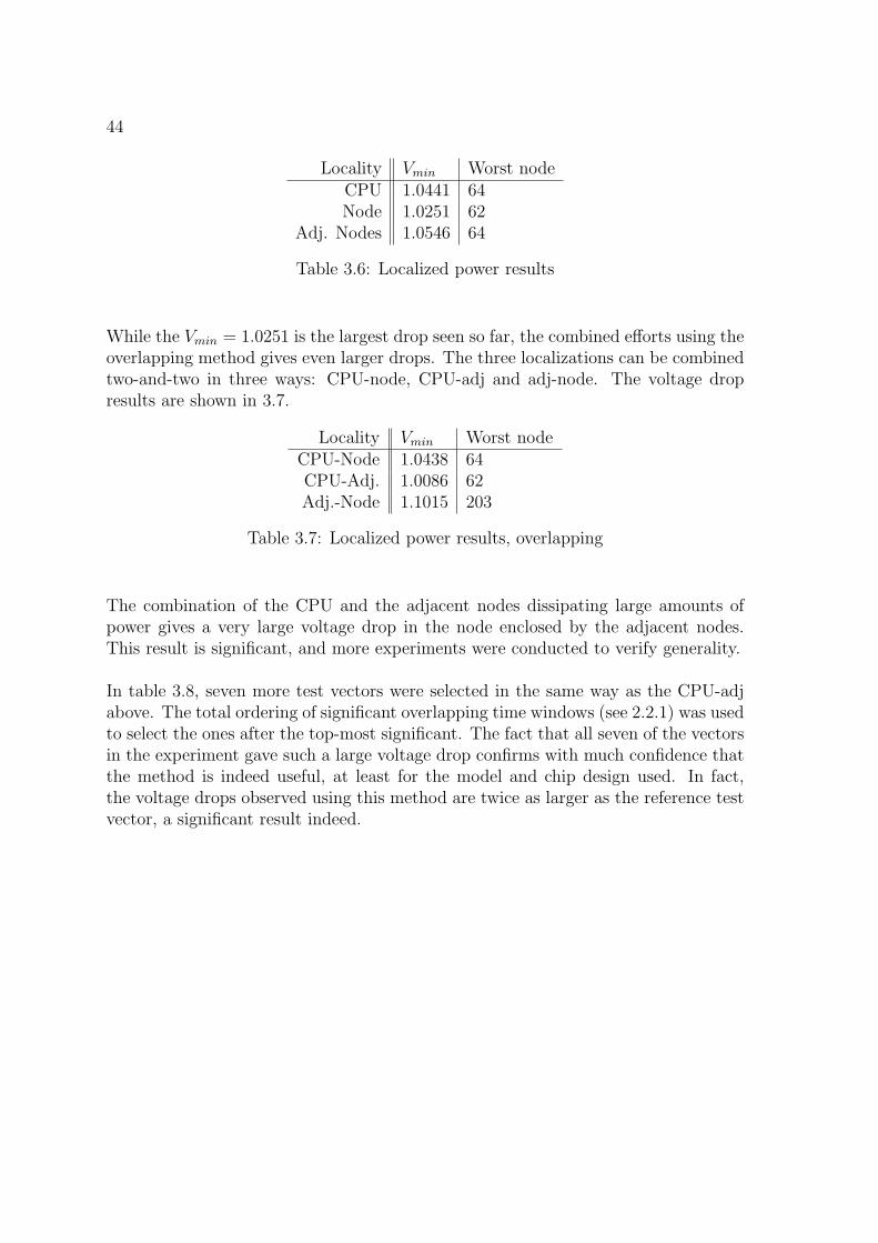
While the Vmin = 1.0251 is the largest drop seen so far, the combined efforts using theoverlapping method gives even larger drops. The three localizations can be combinedtwo-and-two in three ways: CPU-node, CPU-adj and adj-node. The voltage dropresults are shown in 3.7.
Locality Vmin Worst nodeCPU-Node 1.0438 64CPU-Adj. 1.0086 62Adj.-Node 1.1015 203
Table 3.7: Localized power results, overlapping
The combination of the CPU and the adjacent nodes dissipating large amounts ofpower gives a very large voltage drop in the node enclosed by the adjacent nodes.This result is significant, and more experiments were conducted to verify generality.
In table 3.8, seven more test vectors were selected in the same way as the CPU-adjabove. The total ordering of significant overlapping time windows (see 2.2.1) was usedto select the ones after the top-most significant. The fact that all seven of the vectorsin the experiment gave such a large voltage drop confirms with much confidence thatthe method is indeed useful, at least for the model and chip design used. In fact,the voltage drops observed using this method are twice as larger as the reference testvector, a significant result indeed.

45
No. Vmin Worst node1 1.0086 622 1.0088 623 1.0087 624 1.0087 625 1.0088 626 1.0086 627 1.0084 62
Table 3.8: CPU and adjacent nodes overlapping time windows, Voltage Drops
3.3.1 Choosing the Worst Node
In the results presented above, a “worst node” was assumed. This node was foundthrough performing voltage drop simulation on a lot of different test vectors and not-ing which node most frequently had the largest voltage drop.
Using the methods developed in 2.2.2, other nodes are pointed out as being the worst.This section will document some experiments done while focusing on these nodes.
In figure 2.6(a), node number 76 was shown to have the largest power dissipationover a 1 ns time interval. This should make it interesting from a worst-case dropperspective. Switching information was generated for the time window enclosing the1 ns time interval where the node power peaked and a simulation was performed. Theresults showed that the minimum voltage observed was Vmin = 1.0313 V. This valuecan be compared to Vmin = 1.0251 V from table 3.6. Interestingly, this drop occurredin node 63, and not 76 where the maximum power occurred.
Studying the current of the two nodes (63 and 76) reveals that node 63 had in facta much higher peak current than 76. It also had the maximum current over a 1 nstime interval. This node should thus have been found to be the maximum powerconsuming node.
A possible explanation of this phenomenon is that the 1 ns time interval of PrimeTimePX coincided with the peak in node 63 in such a way that the whole peak was not en-closed in the time interval. This means a finer time resolution must be used to detectpower peaks. The concept of choosing a proper time resolution for peak-power anal-ysis was discussed in section 3.1, and these results further motivate that consideration.
Still, a minimum observed voltage drop of Vmin = 1.0313 V is better than many other

46
methods of finding a worst-case test vector presented here. It is a simple method thatcould be useful in identifying the worst node and at the same time the worst timewindow.
Another interesting node from figures 2.6 and 2.7 is node 63. It is a central point infigure 2.7(b), which indicates a large node/adjacent node power combination. Sim-ulation results yielded Vmin = 1.05 V in node 64 (which is one its adjacent nodes).This results can be partly explained by figure 2.6(b) and 2.7(b). In 2.6(b), 64 has alarger max than 63, and from 2.7(b), 63 has large adjacent nodes. We would expectthis node/time to show a large drop in 64. The voltage drop is rather small, however.
Moving to power traces in 0.1 ns time resolution and the figures 2.8, 2.9 and 2.10,nodes 62 and 64 are the most prominent. The current profile was generated for thetime when node 64 peaks, and was compared to the current profile for the peak ofnode 62. Surprisingly, the time window identified by node 62 had the larger currentthan the time window for node 64. The result is similar to the above paragraphabout node 63 and 64. The issue could possibly be that an even finer time resolutionis required to get a one-to-one mapping between node power dissipation and nodecurrent maximum.
The currents discussed above are plotted in figures 3.2 for the time of the peak ofnode 62, and 3.3 for the time of the peak of node 64. The above plots of the figuresshow current consumption in node 62 while the plots below show the same for node64. From figure 2.8, we would expect figure 3.3 to show a larger maximum currentthan figure 3.2.
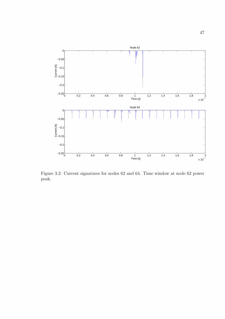
47
0 0.2 0.4 0.6 0.8 1 1.2 1.4 1.6 1.8 2
x 10−7
Cur
rent
[A]
Time [s]
Time [s]
Cur
rent
[A]
−0.25
−0.2
−0.15
−0.1
−0.05
0Node 62
0 0.2 0.4 0.6 0.8 1 1.2 1.4 1.6 1.8 2
x 10−7
−0.25
−0.2
−0.15
−0.1
−0.05
0Node 64
Figure 3.2: Current signatures for nodes 62 and 64. Time window at node 62 powerpeak.
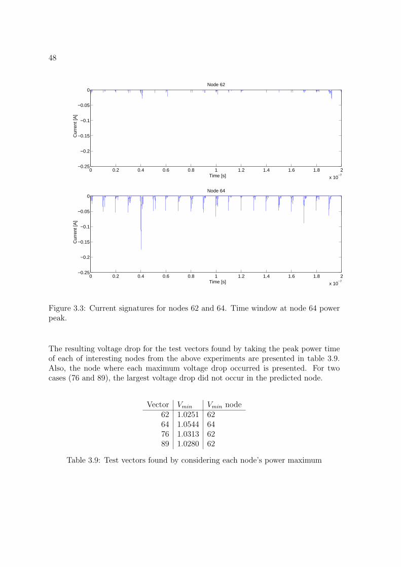
48
Cur
rent
[A]
Time [s]
Time [s]
Cur
rent
[A]
0 0.2 0.4 0.6 0.8 1 1.2 1.4 1.6 1.8 2
x 10−7
−0.25
−0.2
−0.15
−0.1
−0.05
0Node 62
0 0.2 0.4 0.6 0.8 1 1.2 1.4 1.6 1.8 2
x 10−7
−0.25
−0.2
−0.15
−0.1
−0.05
0Node 64
Figure 3.3: Current signatures for nodes 62 and 64. Time window at node 64 powerpeak.
The resulting voltage drop for the test vectors found by taking the peak power timeof each of interesting nodes from the above experiments are presented in table 3.9.Also, the node where each maximum voltage drop occurred is presented. For twocases (76 and 89), the largest voltage drop did not occur in the predicted node.
Vector Vmin Vmin node62 1.0251 6264 1.0544 6476 1.0313 6289 1.0280 62
Table 3.9: Test vectors found by considering each node’s power maximum

49
So far, the results from these power analyses give no particular preference to node 62.It is, however, the top node in 0.1 ns time resolution considering adjacent nodes, asshown in figure 2.9, but the choice of this particular node remains quite arbitrary. Yetit is this node that is the worst node in all test vectors exhibiting a large drop, andfocusing on its power dissipation peak yields the largest voltage drops. This makesthe methodology developed an iterative process rather than an ability to immediatelyforesee where and when the largest drop will occur.
3.4 Voltage Drop Characteristics and Worst-case
Test vectors have been found that have larger maximum voltage drop than the refer-ence vectors. But how do other characteristics of the voltage drop curves compare?In figure 3.4, annotated voltage curves are plotted for the reference vector (3.4(a))and a vector with a higher maximum voltage drop (3.4(b)).
One interesting characteristic is the duration of the voltage drop. A short pulse mighthave other implications for timing than a long drop. Looking at the “Delta X” anno-tation for both plots, we can see that the duration of the large drop is longer for thereference case (a) than for the worst vector case (b). Furthermore, another charac-teristic that can be read from these plots is the time duration where the worst-casedrop in (b) has fallen below the level of the worst-case for the reference vector(a).From the figure, this is approximately two thirds of the voltage drop duration.
Near the right edge of the figures, an annotation on 1.1968 V (close to nominal 1.2V) tells us something of the time to recovery of the drops. Measuring from the lowestV in the figure, for (a), this time is 12 ns while for (b) it is 8 ns.
In other words, while the drop in figure 3.4(b) has the largest maximum, figure 3.4(a)has longer time durations. These differing characteristics might have different impli-cations for timing, which will be discussed later on.
An interesting question is what causes these differences in characteristics. Going backto the current profiles which give rise to the voltage drops hints to a possible answer.Table 3.10 specifies the maximum current of the test vectors in different levels oflocality: 1) full-chip current, 2) superposition of adjacent nodes of worst-case voltagedrop node and the node itself and 3) worst-case voltage drop node itself only.

50
Locality Ref. vector Worst vectorFull-chip 1.9397 1.9211Adj. nodes 0.0774 0.2447Node 0.0724 0.2132
Table 3.10: Current profile max of two test vectors [A]
The full-chip current is larger for the reference vector. This is to be expected, sincethis vector was found by taking the top power consuming clock cycle for a full-chippower trace. For the other levels of locality, the worst vector has the larger maxcurrent. Another thing to note is the difference between the two last localities. Forthe worst vector, this means that its adjacent nodes also have a large current surge.This is not the case for the reference vector.
The above numbers, although perhaps not representative for a general truth, indi-cate that large chip-wide current consumption give slow recovery times while largecurrents in a few local nodes give quick voltage drops of larger magnitude.
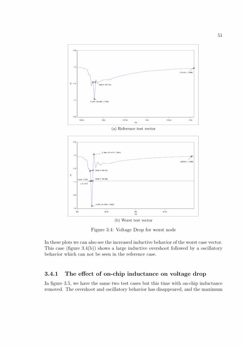
51
(V
)
1.05
1.1
1.15
1.2
1.25
t(s)
102.5n 105n 107.5n 110n 112.5n 115n
X_Min: (103.96n, 1.1034)
(115.41n, 1.1968)
Delta X: 301.31p
(a) Reference test vector
(V
)
1.0
1.05
1.1
1.15
1.2
1.25
t(s)
30n 32.5n 35n 37.5n
(39.801n, 1.1968)
Delta X: 240.01p
Level: 1.1034
x: 31.157n
X_Max: (31.417n, 1.2041)
X_Min: (31.242n, 1.0087)
Delta X: 162.08p
(b) Worst test vector
Figure 3.4: Voltage Drop for worst node
In these plots we can also see the increased inductive behavior of the worst case vector.This case (figure 3.4(b)) shows a large inductive overshoot followed by a oscillatorybehavior which can not be seen in the reference case.
3.4.1 The effect of on-chip inductance on voltage drop
In figure 3.5, we have the same two test cases but this time with on-chip inductanceremoved. The overshoot and oscillatory behavior has disappeared, and the maximum

52
voltage drop is much lower.
For the reference case (3.5(b)), the maximum drop has also decreased. However, sincethere was not much inductive behavior with inductance, the shape of the drop hasnot changed much.
Quantifying the impact of the on-chip inductance for the two cases reveals the follow-ing. For the reference vector, the addition of on-chip inductance caused the voltagedrop to increase from 75 mV to 96 mV, or about 29%. For the worst-case vector,on-chip inductance caused the voltage drop to increase from 112 mV to 191 mV, or71%. This result shows a huge increase in estimation of the importance of on-chipinductance. In [1], it was concluded (with the same model used in this thesis) thatinclusion of on-chip inductance can increase the voltage drop by over 50%. By simplyapplying a different test vector to the very same model, it has now been shown thaton-chip inductance can increase the voltage drop by 70%.
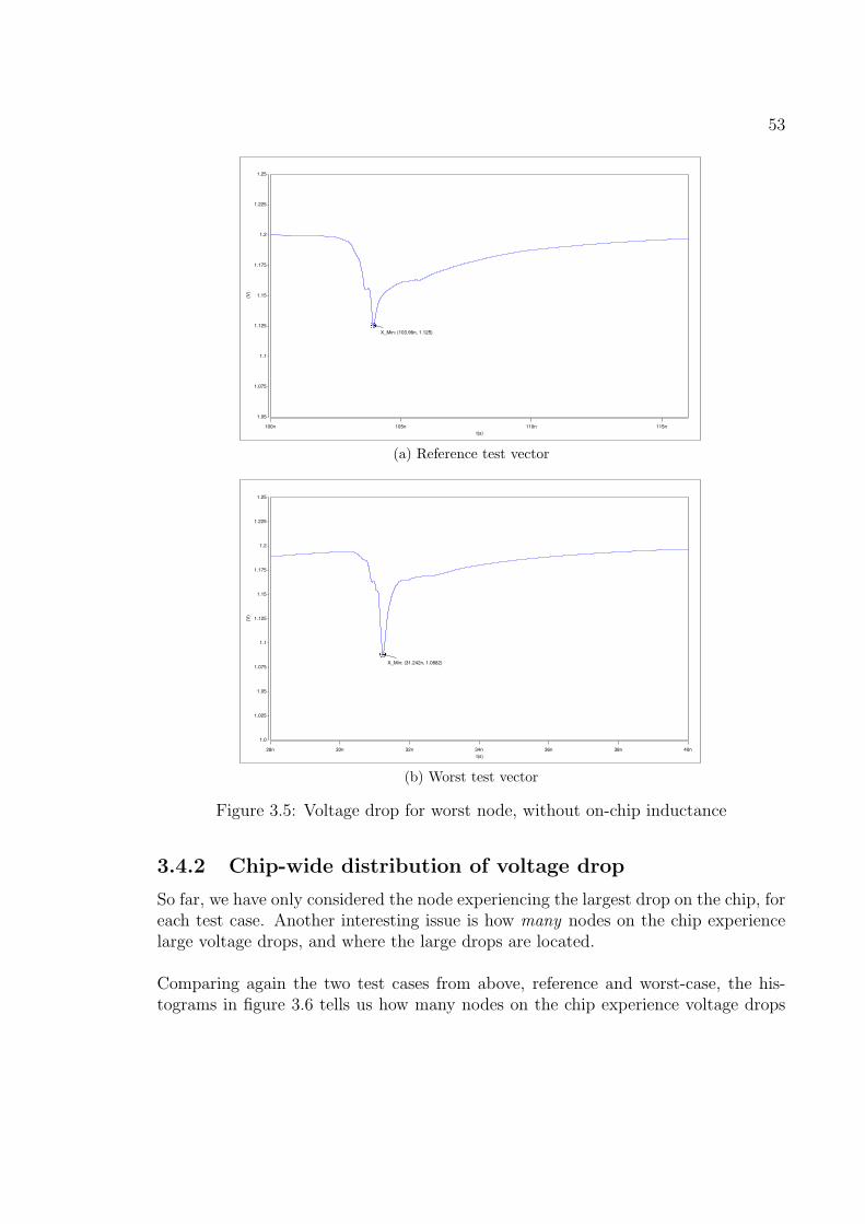
53
(V
)
1.05
1.075
1.1
1.125
1.15
1.175
1.2
1.225
1.25
t(s)
100n 105n 110n 115n
X_Min: (103.96n, 1.125)
(a) Reference test vector
(V
)
1.0
1.025
1.05
1.075
1.1
1.125
1.15
1.175
1.2
1.225
1.25
t(s)
28n 30n 32n 34n 36n 38n 40n
X_Min: (31.242n, 1.0882)
(b) Worst test vector
Figure 3.5: Voltage drop for worst node, without on-chip inductance
3.4.2 Chip-wide distribution of voltage drop
So far, we have only considered the node experiencing the largest drop on the chip, foreach test case. Another interesting issue is how many nodes on the chip experiencelarge voltage drops, and where the large drops are located.
Comparing again the two test cases from above, reference and worst-case, the his-tograms in figure 3.6 tells us how many nodes on the chip experience voltage drops
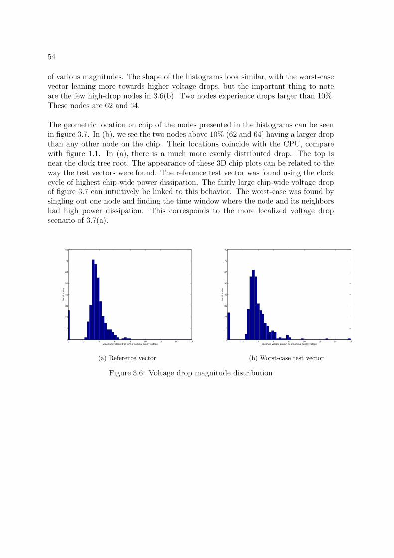
54
of various magnitudes. The shape of the histograms look similar, with the worst-casevector leaning more towards higher voltage drops, but the important thing to noteare the few high-drop nodes in 3.6(b). Two nodes experience drops larger than 10%.These nodes are 62 and 64.
The geometric location on chip of the nodes presented in the histograms can be seenin figure 3.7. In (b), we see the two nodes above 10% (62 and 64) having a larger dropthan any other node on the chip. Their locations coincide with the CPU, comparewith figure 1.1. In (a), there is a much more evenly distributed drop. The top isnear the clock tree root. The appearance of these 3D chip plots can be related to theway the test vectors were found. The reference test vector was found using the clockcycle of highest chip-wide power dissipation. The fairly large chip-wide voltage dropof figure 3.7 can intuitively be linked to this behavior. The worst-case was found bysingling out one node and finding the time window where the node and its neighborshad high power dissipation. This corresponds to the more localized voltage dropscenario of 3.7(a).
0 2 4 6 8 10 12 14 160
10
20
30
40
50
60
70
80
No.
of n
odes
Maximum voltage drop in % of nominal supply voltage
(a) Reference vector
0 2 4 6 8 10 12 14 160
10
20
30
40
50
60
70
80
Maximum voltage drop in % of nominal supply voltage
No.
of n
odes
(b) Worst-case test vector
Figure 3.6: Voltage drop magnitude distribution
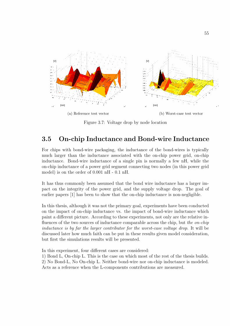
55
[V]
[nm]
(a) Reference test vector
[V]
[nm]
(b) Worst-case test vector
Figure 3.7: Voltage drop by node location
3.5 On-chip Inductance and Bond-wire Inductance
For chips with bond-wire packaging, the inductance of the bond-wires is typicallymuch larger than the inductance associated with the on-chip power grid, on-chipinductance. Bond-wire inductance of a single pin is normally a few nH, while theon-chip inductance of a power grid segment connecting two nodes (in this power gridmodel) is on the order of 0.001 nH - 0.1 nH.
It has thus commonly been assumed that the bond wire inductance has a larger im-pact on the integrity of the power grid, and the supply voltage drop. The goal ofearlier papers [1] has been to show that the on-chip inductance is non-negligible.
In this thesis, although it was not the primary goal, experiments have been conductedon the impact of on-chip inductance vs. the impact of bond-wire inductance whichpaint a different picture. According to these experiments, not only are the relative in-fluences of the two sources of inductance comparable across the chip, but the on-chipinductance is by far the larger contributor for the worst-case voltage drop. It will bediscussed later how much faith can be put in these results given model consideration,but first the simulations results will be presented.
In this experiment, four different cases are considered:1) Bond L, On-chip L. This is the case on which most of the rest of the thesis builds.2) No Bond-L, No On-chip L. Neither bond-wire nor on-chip inductance is modeled.Acts as a reference when the L-components contributions are measured.

56
3) Bond L, No On-chip L. Only the bond-wire inductance is modeled.4) No Bond L, On-Chip L. Only the on-chip inductance is modeled.
In figure 3.8, simulation results for two randomly chosen nodes are shown for the fourcases. In figure 3.8(a), bond-wire inductance has a larger impact on voltage drop thandoes the on-chip inductance. For figure 3.8(b) however, it is the on-chip inductancethat contributes the most to the voltage drop. The on-chip inductance adds 28.6% tothe voltage drop without inductance. Bond-wire inductance adds 0.2% to the voltagedrop. In (a), the randomly chosen node is in the M3 layer while (b) is in M1 whichdirectly supplies the transistors. This layer dependence seems to be general for thedesign, as is summarized in table 3.11. Here, the number of nodes that have BondL and On-Chip L, respectively, as their main voltage drop contributors is stated foreach metal layer of the model.
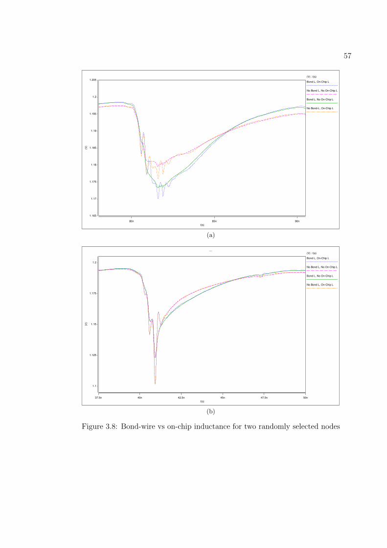
57
(V
)
1.165
1.17
1.175
1.18
1.185
1.19
1.195
1.2
1.205
t(s)
80n 85n 90n
(V) : t(s)
Bond L, On−Chip L
No Bond L, No On−Chip L
Bond L, No On−Chip L
No Bond−L, On−Chip L
(a)
__
(V
)
1.1
1.125
1.15
1.175
1.2
t(s)
37.5n 40n 42.5n 45n 47.5n 50n
(V) : t(s)
Bond L, On−Chip L
No Bond L, No On−Chip L
Bond L, No On−Chip L
No Bond L, On−Chip L
(b)
Figure 3.8: Bond-wire vs on-chip inductance for two randomly selected nodes
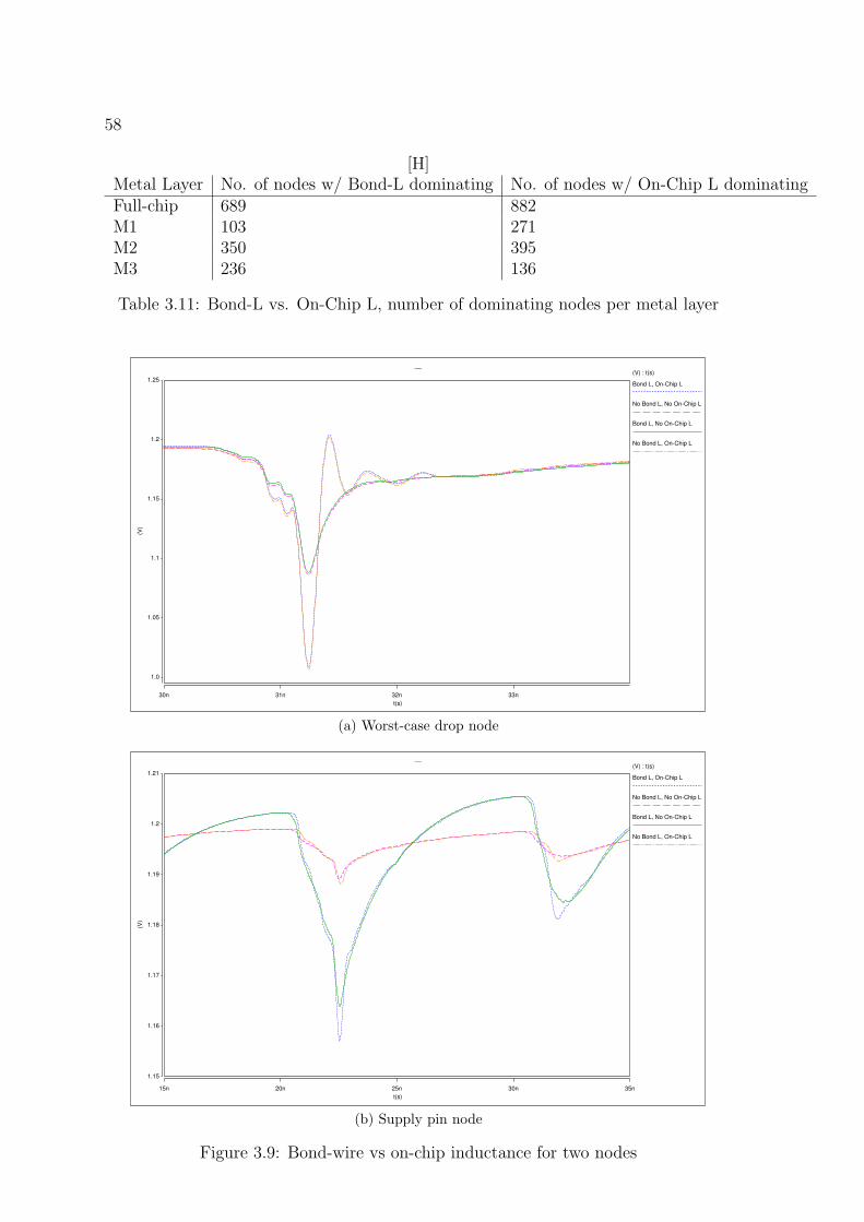
58
[H]Metal Layer No. of nodes w/ Bond-L dominating No. of nodes w/ On-Chip L dominatingFull-chip 689 882M1 103 271M2 350 395M3 236 136
Table 3.11: Bond-L vs. On-Chip L, number of dominating nodes per metal layer
__
(V
)
1.0
1.05
1.1
1.15
1.2
1.25
t(s)
30n 31n 32n 33n
(V) : t(s)
Bond L, On−Chip L
No Bond L, No On−Chip L
Bond L, No On−Chip L
No Bond L, On−Chip L
(a) Worst-case drop node
__
(V
)
1.15
1.16
1.17
1.18
1.19
1.2
1.21
t(s)
15n 20n 25n 30n 35n
(V) : t(s)
Bond L, On−Chip L
No Bond L, No On−Chip L
Bond L, No On−Chip L
No Bond L, On−Chip L
(b) Supply pin node
Figure 3.9: Bond-wire vs on-chip inductance for two nodes

59
In figure 3.9(a), the same comparison is repeated for the node with the largest voltagedrop. Here, the contribution of bond-wire inductance is dwarfed by the on-chipinductance. Figure 3.9(b) shows a node sitting at a supply pin. It shows the expectedresult that bond-wire inductance is more significant here. The worst-node case isparticularly interesting. It shows us that a large part of the worst voltage dropidentified on the chip is an L dI/dt drop caused by the on-chip inductance. In fact,the bond-wire inductance seems to slightly decrease the drop. Putting the result intonumbers tells us that case 4 has a 70% larger voltage drop than case 2, while case 3has a 1% smaller voltage drop than case two. Comparing this result with that of figure3.8(b) shows us that on-chip inductance has a much larger relative impact in the worstcase than for a randomly chosen node. The values of extracted inductances close tothese nodes are similar so the reason for the difference must be found elsewhere.
3.5.1 Frequency Components and Inductance Contributions
Bond-wire inductance generally result in chip-wide voltage fluctuations while on-chipinductance usually cause spatially localized variations. The chip-wide disturbancestranslate to a low frequency voltage drop curve while localized behavior usually con-sist of higher frequencies.
In order to test this hypothesis in the context of the model used in this thesis, anexperiment was conducted on the influence of bond-wire vs on-chip inductance ondifferent frequency components of a voltage drop waveform.
Using FFT based techniques, the voltage drop waveform for each node on the chipwas filtered to extract the low-frequency components and the high-frequency compo-nents. The division into frequency components is illustrated in figure 3.10, where theworst-case drop node is plotted for bond-wire L only (a) and on-chip L only (b).
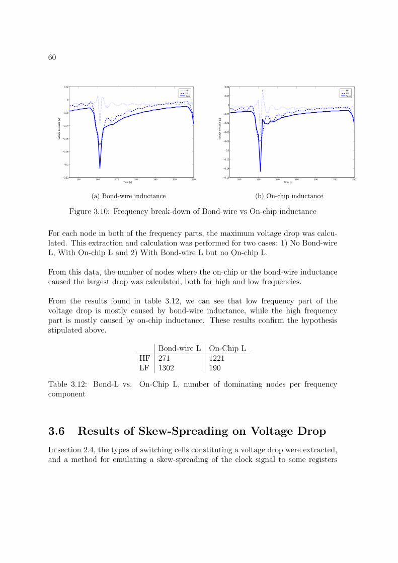
60
Time [s]
Vol
tage
dev
iatio
n [V
]
150 160 170 180 190 200 210−0.12
−0.1
−0.08
−0.06
−0.04
−0.02
0
0.02
HFLFSum
(a) Bond-wire inductance
Time [s]
Vol
tage
dev
iatio
n [V
]
150 160 170 180 190 200 210−0.16
−0.14
−0.12
−0.1
−0.08
−0.06
−0.04
−0.02
0
0.02
0.04
HFLFSum
(b) On-chip inductance
Figure 3.10: Frequency break-down of Bond-wire vs On-chip inductance
For each node in both of the frequency parts, the maximum voltage drop was calcu-lated. This extraction and calculation was performed for two cases: 1) No Bond-wireL, With On-chip L and 2) With Bond-wire L but no On-chip L.
From this data, the number of nodes where the on-chip or the bond-wire inductancecaused the largest drop was calculated, both for high and low frequencies.
From the results found in table 3.12, we can see that low frequency part of thevoltage drop is mostly caused by bond-wire inductance, while the high frequencypart is mostly caused by on-chip inductance. These results confirm the hypothesisstipulated above.
Bond-wire L On-Chip LHF 271 1221LF 1302 190
Table 3.12: Bond-L vs. On-Chip L, number of dominating nodes per frequencycomponent
3.6 Results of Skew-Spreading on Voltage Drop
In section 2.4, the types of switching cells constituting a voltage drop were extracted,and a method for emulating a skew-spreading of the clock signal to some registers
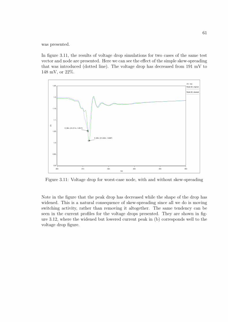
61
was presented.
In figure 3.11, the results of voltage drop simulations for two cases of the same testvector and node are presented. Here we can see the effect of the simple skew-spreadingthat was introduced (dotted line). The voltage drop has decreased from 191 mV to148 mV, or 22%.
(V
)
0.9
0.95
1.0
1.05
1.1
1.15
1.2
1.25
t(s)
30n 31n 32n 33n 34n 35n
X_Min: (31.242n, 1.0087)
X_Min: (31.211n, 1.0517)
(V) : t(s)
Node 62, original
Node 62, skewed
Figure 3.11: Voltage drop for worst-case node, with and without skew-spreading
Note in the figure that the peak drop has decreased while the shape of the drop haswidened. This is a natural consequence of skew-spreading since all we do is movingswitching activity, rather than removing it altogether. The same tendency can beseen in the current profiles for the voltage drops presented. They are shown in fig-ure 3.12, where the widened but lowered current peak in (b) corresponds well to thevoltage drop figure.
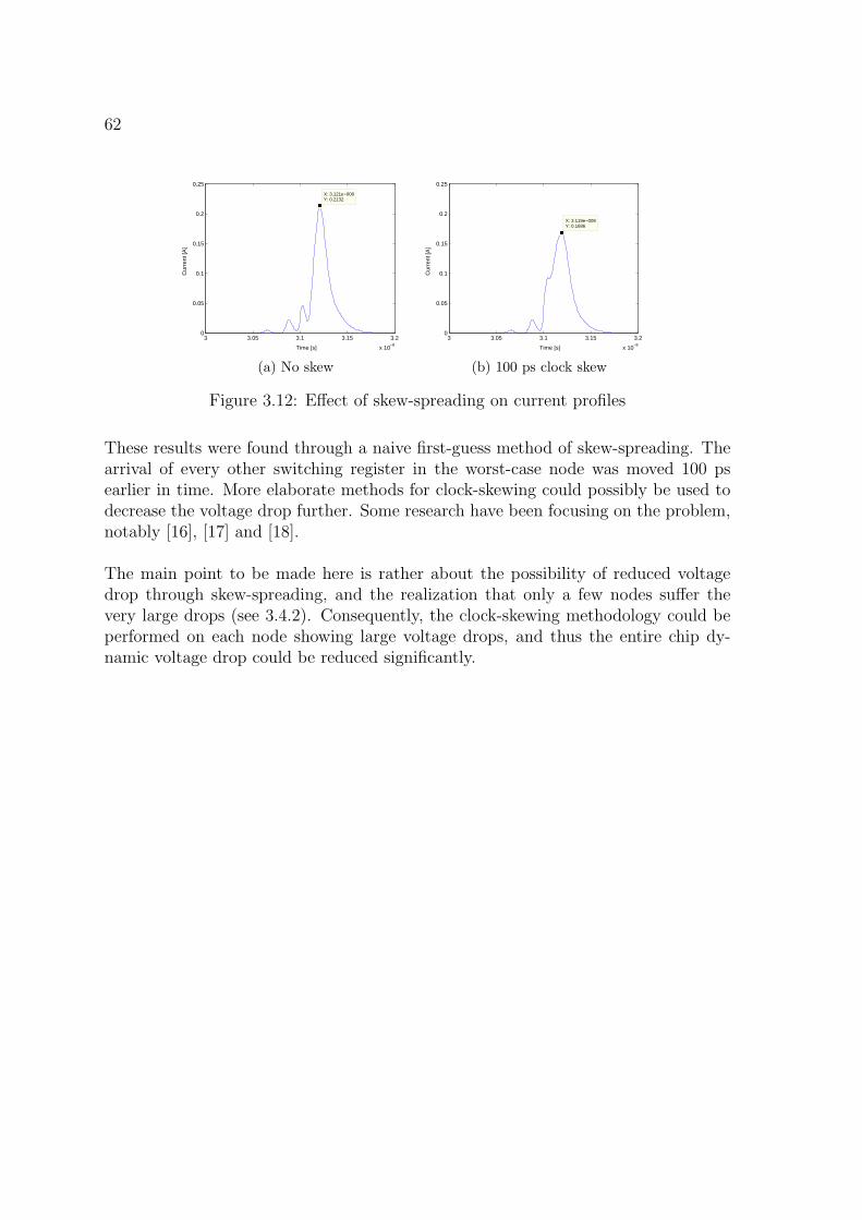
62
3 3.05 3.1 3.15 3.2
x 10−8
Cur
rent
[A]
Time [s]
0
0.05
0.1
0.15
0.2
0.25
X: 3.121e−008Y: 0.2132
(a) No skew
Cur
rent
[A]
Time [s]
3 3.05 3.1 3.15 3.2
x 10−8
0
0.05
0.1
0.15
0.2
0.25
X: 3.119e−008Y: 0.1686
(b) 100 ps clock skew
Figure 3.12: Effect of skew-spreading on current profiles
These results were found through a naive first-guess method of skew-spreading. Thearrival of every other switching register in the worst-case node was moved 100 psearlier in time. More elaborate methods for clock-skewing could possibly be used todecrease the voltage drop further. Some research have been focusing on the problem,notably [16], [17] and [18].
The main point to be made here is rather about the possibility of reduced voltagedrop through skew-spreading, and the realization that only a few nodes suffer thevery large drops (see 3.4.2). Consequently, the clock-skewing methodology could beperformed on each node showing large voltage drops, and thus the entire chip dy-namic voltage drop could be reduced significantly.

Chapter 4
Discussion
Test vectors leading to large voltage drops have been found, and a methodologyof finding them has been developed. This section discusses the problems involvedin drawing definite conclusions on the results and suggests future work that couldfurther the process of understanding power integrity.
4.1 Weaknesses in Model and Methodology
While the developed methodology for identifying worst-case input test vectors froma large simulation trace proved successful in this context, it is too early to say that itwill be as successful for other models or for other designs. Since no similar model foranother design existed at the time that the experiments were conducted, it cannot besaid with certainty that the methods developed here would show the same result foranother design with a different power grid topology.
Within the same design, more test cases should also be analyzed. Perhaps the devel-oped methodology proves to be the best for identifying worst-cases for those test-casestoo, but other test-cases could show even larger drops than those found here. It wouldbe good to analyze run traces of real in-field use-case data to establish if the usedsimulation trace is representative in terms of voltage drop tendencies.
It has been argued that the model used in this thesis has weaknesses that could intro-duce too much uncertainty in the result, especially considering quantitative results.For instance, in this thesis the ground net has been neglected. Depending on thepower/ground grid topology, this could lead to overestimating or underestimatingthe impact of on-chip inductance. Currents flowing in opposite directions of wireswith large mutual inductance would cause smaller loop inductance, according to [19].The paired grid-approached to power planning places conductors with opposite cur-rent (vdd/gnd) close to each other, which should increase this effect.
63
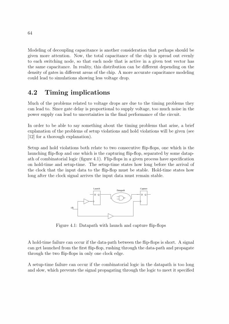
64
Modeling of decoupling capacitance is another consideration that perhaps should begiven more attention. Now, the total capacitance of the chip is spread out evenlyto each switching node, so that each node that is active in a given test vector hasthe same capacitance. In reality, this distribution can be different depending on thedensity of gates in different areas of the chip. A more accurate capacitance modelingcould lead to simulations showing less voltage drop.
4.2 Timing implications
Much of the problems related to voltage drops are due to the timing problems theycan lead to. Since gate delay is proportional to supply voltage, too much noise in thepower supply can lead to uncertainties in the final performance of the circuit.
In order to be able to say something about the timing problems that arise, a briefexplanation of the problems of setup violations and hold violations will be given (see[12] for a thorough explanation).
Setup and hold violations both relate to two consecutive flip-flops, one which is thelaunching flip-flop and one which is the capturing flip-flop, separated by some datap-ath of combinatorial logic (figure 4.1). Flip-flops in a given process have specificationon hold-time and setup-time. The setup-time states how long before the arrival ofthe clock that the input data to the flip-flop must be stable. Hold-time states howlong after the clock signal arrives the input data must remain stable.
clk
DatapathLaunch Capture
QD QD
Figure 4.1: Datapath with launch and capture flip-flops
A hold-time failure can occur if the data-path between the flip-flops is short. A signalcan get launched from the first flip-flop, rushing through the data-path and propagatethrough the two flip-flops in only one clock edge.
A setup-time failure can occur if the combinatorial logic in the datapath is too longand slow, which prevents the signal propagating through the logic to meet it specified
65
setup-time, when it should have settled at the input of the capturing flip-flop.
In this thesis, the min (or fast) corner of PVT has been used. That means the simu-lation results apply for the case of high voltage and low temperature. For this reason,the hold-time failures are the most interesting, because setup-time failures are un-likely to occur with the fast propagation of the min corner. Setup-timing problemswould be more likely to occur if we had large voltage drops in the later part of a clockcycle, since this is when the combinatorial logic in the datapath between sequentialelements switch.
Also, the goal of finding the worst-case test vector has been to find the maximumvoltage drop, not worrying so much about when in a specific clock cycle it occurs.Since the maximum drops tended to be in the flip-flop switching point of the cycle,they are more likely to cause hold-time failures. Focusing on the hold-time failures,how can the worst-case voltage drop translate to timing implications?
The most hazardous situation for hold-time occurs when the clock path between twosubsequent flip-flops is short, so that there is a small margin for any skewing intro-duced in the clock signals propagating towards the flip-flops. In this situation, if theclock buffers of the capturing flip-flops clock path should experience a voltage dropsignificantly larger than that of the launching flip-flop, a hold-time failure could occur(see figure 4.1).
Refer to figure 2.13, where a typical voltage drop waveform is shown with annotationof different parts of the voltage drop. Table 2.3 shows the distribution of types ofcells. The “deepest” spike of the drop consists mainly of flip-flops, as was discussed.However, before the deepest spike, a certain part of the large drop is often made upof clock buffer cells. These clock buffers could, since they are in the same node andtherefore located close to each other, be sensitive to voltage variation from a hold-time violation point of view.
Further work needs to be done to be able to say something conclusive about thetiming impacts of the voltage drops found in this thesis. For example, in order toinvestigate the difference in voltage drop between clock buffers of launch/capture flip-flops clock path, the model needs to be made more fine grained. Today, the modelwould probably include the voltage drop of both these clock buffers in the same nodeand therefore voltage drop waveform.
By knowing the location of large voltage drops, and by knowing the exact time whenthey will occur, more detailed analyses can be made based on this knowledge. FromSTA (Static Timing Analysis) tools, the most critical hold-time paths can be ex-

66
tracted. If any of these happen in the area of large voltage drop, this path can besimulated with a gate-level netlist using current data from the small part of the VCDextracted through the use of the methodology developed here.
While the worst-case vectors found in this work give a pessimistic view of the powergrid studied, the chip design is known to work satisfactory even with these powersupply drops. The results do not directly help to reduce the pessimism of corner-based design, since they tell us the drops are larger than expected, but they doincrease understanding of dynamic behavior in a power supply grid.
4.3 Consequences for design flow
This thesis has established a methodology for finding a worst-case test vector formaximized voltage drop. But how does this finding relate to the standard practice ofdesign and sign-off in a real project?
In the introductory chapter, the practice of performing static IR drop analyses wasexplained. In this context, transient and localized behaviors are not captured. Circuitperformance is usually derated in order to account for a conservative value of supplyvoltage noise. With detailed dynamic voltage drop studies, this pessimism could pos-sibly be reduced. Some EDA tools also include dynamic IR drop analyses, which areusually vector based. A sign-off team working in a dynamic IR drop analysis settingcould use the developed method to find a worst-case for their design and use as inputfor the dynamic analysis.
An interesting experiment would be to compare the dynamic voltage drops found byEDA tools to those found using SPICE as was done in this thesis. Even if the mag-nitudes of the drops are not the same, the relative voltage drops between worst-casevectors and random vectors should be investigated. If the same tendency of differencebetween worst-case and random vectors is seen in commercial EDA tools as in themodel in this thesis, then that adds to the usefulness of the developed methodology.
A problem with this methodology of finding a worst-case test vector for a design, isthat a floorplanned design late in the design flow must be used. At this point it couldbe troublesome to introduce changes to the design to deal with the large voltage dropsfound.
67
4.4 Conclusions
Voltage drops in the model of a power supply grid have been simulated using differentinput test vectors. The voltage drops found were shown to have a large dependencyon the choice of test vectors. It was also shown that the test vector extracted byfinding the most power consuming clock cycle resulted in a voltage drop that wasmuch smaller than those found using other methods.
Time-resolution in calculating power consumption is very significant. Using a slightlyfiner resolution in full-chip power calculations revealed a 60% voltage drop increase.
Frequency-content of the full-chip power consumption turned out to have little or noeffect on voltage drop.
The best method for identifying test vectors leading to large voltage drops turned outto be combining different areas of spatial locality around a geometric point on thechip which was known to experience particularly high voltage drops. The single bestmethod was to choose the points in time when nodes adjacent to the known worstnode dissipate much power while at the same time the area making up the CPUdissipates much power. Using this methodology, voltage drops of 16% of the nominalsupply voltage were found, a voltage drop that is twice that of the reference case.
The process of identifying the worst node remains iterative. It is difficult to statewith confidence a general method of identifying this node. Performing several SPICEsimulations and observing which node experiences the largest drop will probably benecessary if the methodology should be applied to a different design.
The fact that voltage drops were found that should have been too large for the chipto function, shows that there is still a lot we do not understand about the powersupply of an integrated circuit and the timing implications of noise in the grid. Thetopic remains active in research, and should continue to do so since process scalingand lowered supply voltages make power integrity more problematic.
The input-dependent nature of dynamic power grid analyses makes it natural toconsider the worst time instance of a simulation run. This thesis has developedmethods for extracting worst-case test vectors which can add a piece to the puzzle ofpower integrity analysis.

Bibliography
[1] Andersson, D.A., Nilsson, B., Pihl, J., Svensson, L., and Larsson-Edefors, P.,“Supply voltage drop study considering on-chip self inductance of a 32-bit pro-cessor’s power grid,” Signal Propagation on Interconnects, 2009. SPI ’09. IEEEWorkshop on, 12-15 2009
[2] Andersson, D.A., Svensson, L.J., and Larsson-Edefors, P., “Toward a systematicsensitivity analysis of on-chip power grids using factor analysis,” Signal Propa-gation on Interconnects, 2007. SPI 2007. IEEE Workshop on, 13-16 2007
[3] Andersson, Daniel A., Svensson, Lars J., and Larsson-Edefors, Per, “Noise-AwareOn-Chip Power Grid Considerations Using a Statistical Approach,” ISQED ’08:Proceedings of the 9th international symposium on Quality Electronic Design,IEEE Computer Society, Washington, DC, USA, ISBN 978-0-7695-3117-5, 2008
[4] Svensson, L., Pihl, J., Andersson, D.A., Nilsson, B., and Larsson-Edefors, P.,“Towards supply-grid-based derating of timing margins,” Signal Propagation onInterconnects, 2009. SPI ’09. IEEE Workshop on, 12-15 2009
[5] Nilsson, B., Integrated Circuit Supply Noise Study Based on an Extensive PowerGrid Model, Master’s thesis, Chalmers University of Technology, January 2009
[6] Popovich, Mikhail, Mezhiba, Andrey V., and Friedman, Eby G., Power Distri-bution Networks with On-Chip Decoupling Capacitors, chapter 6, Springer Pub-lishing Company, Incorporated, ISBN 0387716009, 9780387716008, pp. 125–174,2007
[7] Pant, Sanjay and Blaauw, D., “Static timing analysis considering power supplyvariations,” Computer-Aided Design, 2005. ICCAD-2005. IEEE/ACM Interna-tional Conference on, 6-10 2005
[8] Nithin, S.K., Shanmugam, G., and Chandrasekar, S., “Dynamic voltage (IR)drop analysis and design closure: Issues and challenges,” Quality Electronic De-sign (ISQED), 2010 11th International Symposium on, ISSN 1948-3287, 22-242010
68
69
[9] Synopsys, PrimeTime PX User Guide Version C-2009.06, 2009
[10] Cheng, Wheling, Sarkar, Aveek, Lin, Shen, and Zheng, Ji, “Worst Case Switchingpattern for Core Noise Analysis,” DesignCon 2009, 2009
[11] Dekking, F.M., Kraaikamp, C., Lopuhaa, H.P., and Meester, L.E., A ModernIntroduction to Probability and Statistics, chapter 10, Springer Publishing Com-pany, Incorporated, pp. 135–150, 2005
[12] Weste, N and Harris, D, CMOS VLSI Design: A Circuits and Systems Perspec-tive, chapter 12, 3rd edition, Pearson Edu., pp. 767–780, 2005
[13] Ferzli, I. A., Chiprout, E., and Najm, F. N., “Verification and Codesign of thePackage and Die Power Delivery System Using Wavelets,” Computer Aided De-sign of Integrated Circuits and Systems IEEE Transactions on, volume 29, no. 1,pp. 92 –102, ISSN 0278-0070, jan. 2010
[14] Addison, Paul S., The Illustrated Wavelet Transform Handbook, Taylor & Fran-cis, 2002
[15] Joseph, Russ, Hu, Zhigang, and Martonosi, Margaret, “Wavelet Analysis for Mi-croprocessor Design: Experiences with Wavelet-Based dI/dt Characterization,”HPCA ’04: Proceedings of the 10th International Symposium on High Perfor-mance Computer Architecture, IEEE Computer Society, Washington, DC, USA,ISBN 0-7695-2053-7, 2004
[16] Vuillod, P., Benini, L., Bogliolo, A., and De Micheli, G., “Clock-skew optimiza-tion for peak current reduction,” Low Power Electronics and Design, 1996.,International Symposium on, 12-14 1996
[17] Vittal, A., Ha, H., Brewer, F., and Marek-Sadowska, M., “Clock skew optimiza-tion for ground bounce control,” Computer-Aided Design, 1996. ICCAD-96. Di-gest of Technical Papers., 1996 IEEE/ACM International Conference on, 10-141996
[18] Nieh, Yow-Tyng, Huang, Shih-Hsu, and Hsu, Sheng-Yu, “Minimizing peak cur-rent via opposite-phase clock tree,” Design Automation Conference, 2005. Pro-ceedings. 42nd, 13-17 2005
[19] Mezhiba, A.V. and Friedman, E.G., “Inductive properties of high-performancepower distribution grids,” Very Large Scale Integration VLSI Systems IEEETransactions on, volume 10, no. 6, pp. 762 – 776, ISSN 1063-8210, dec 2002