Embed Size (px)
Citation preview
Faut-Tolerant Digital System Design week-1 ١
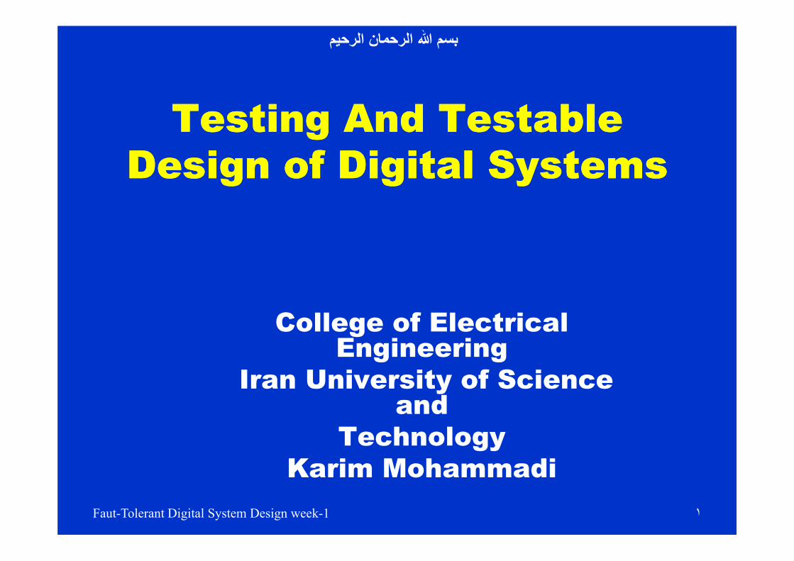
Testing And Testable Design of Digital Systems
Testing And Testable Design of Digital Systems
College of Electrical Engineering
Iran University of Science and
TechnologyKarim Mohammadi
بسم هللا الرحمان الرحيم

VLSI Test: Lecture 1 ٢
Course OutlinePart I: Introduction
Course OutlinePart I: Introduction
Basic concepts and definitions (Chapter 1) Test process and ATE (Chapter 2) Test economics and product quality
(Chapter 3) Fault modeling (Chapter 4)

VLSI Test: Lecture 1 ٣
Course Outline (Cont.)Part II: Test MethodsCourse Outline (Cont.)Part II: Test Methods
Logic and fault simulation (Chapter 5) Testability measures (Chapter 6) Combinational circuit ATPG (Chapter 7) Sequential circuit ATPG (Chapter 8) Memory test (Chapter 9) Analog test (Chapters 10 and 11) Delay test and IDDQ test (Chapters 12 and
13)

VLSI Test: Lecture 1 ٤
Course Outline (Cont.)Part III: DFT
Course Outline (Cont.)Part III: DFT
Scan design (Chapter 14) BIST (Chapter 15) Boundary scan and analog test bus
(Chapters 16 and 17) System test and core-based design (Chapter
18)
٥
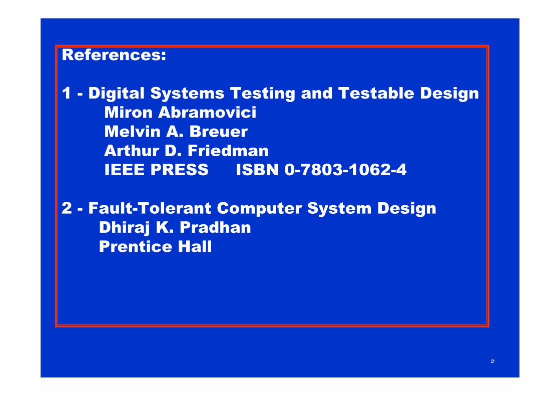
References:
1 - Digital Systems Testing and Testable DesignMiron AbramoviciMelvin A. BreuerArthur D. FriedmanIEEE PRESS ISBN 0-7803-1062-4
2 - Fault-Tolerant Computer System DesignDhiraj K. PradhanPrentice Hall

Faut-Tolerant Digital System Design week-1 ٦
3 - Essentials of Electronic TestingFor Digital, Memory and Mixed-Signal VLSI Circuits
Michael L. BushnellVishwani D. AgrawalKluwer Academic PublisherBoston/ Dordrecht/London
4- Appendix C : Books On Testng
VLSI Test: Lecture 1 ٧
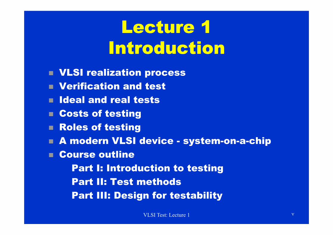
Lecture 1Introduction
Lecture 1Introduction
VLSI realization process Verification and test Ideal and real tests Costs of testing Roles of testing A modern VLSI device - system-on-a-chip Course outline
Part I: Introduction to testingPart II: Test methodsPart III: Design for testability
VLSI Test: Lecture 1 ٨
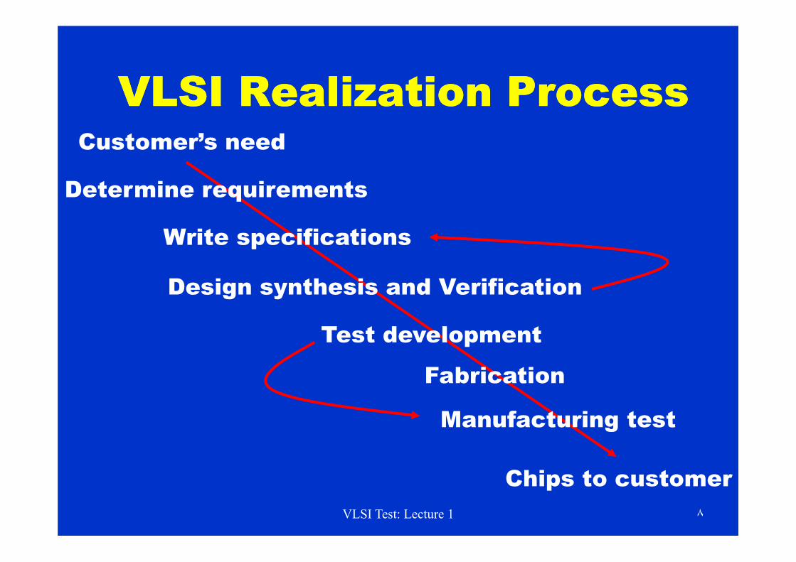
VLSI Realization ProcessVLSI Realization Process
Determine requirements
Write specifications
Design synthesis and Verification
Fabrication
Manufacturing test
Chips to customer
Customer’s need
Test development

VLSI Test: Lecture 1 ٩
DefinitionsDefinitions Design synthesis: Given an I/O function, develop
a procedure to manufacture a device using known materials and processes.
Verification: Predictive analysis to ensure that the synthesized design, when manufactured, will perform the given I/O function.
Test: A manufacturing step that ensures that the physical device, manufactured from the synthesized design, has no manufacturing defect.
10
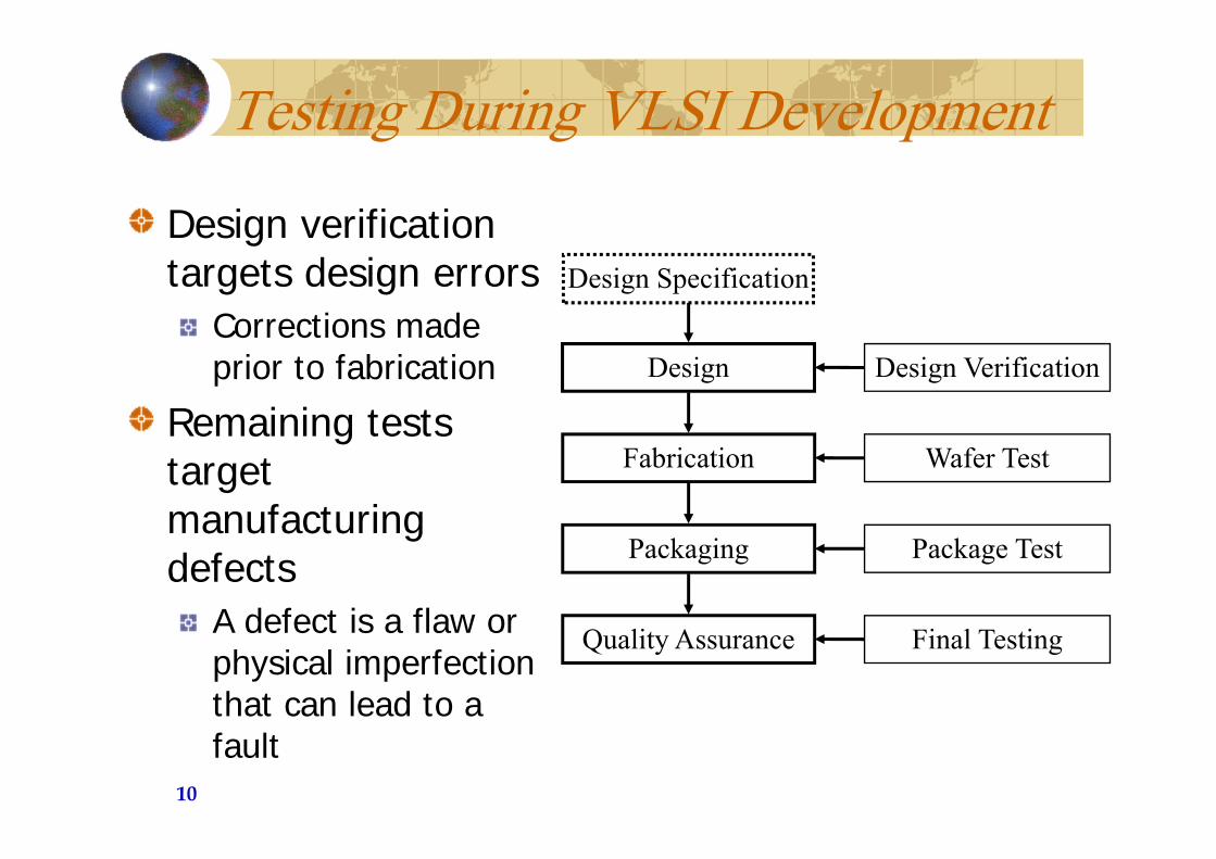
Testing During VLSI Development
Design verification targets design errors
Corrections made prior to fabrication
Remaining tests target manufacturing defects
A defect is a flaw or physical imperfection that can lead to a fault
Design Verification
Wafer Test
Final Testing
Package Test
Design Specification
Design
Fabrication
Quality Assurance
Packaging

11
Design VerificationDifferent levels of abstraction during design
CAD tools used to synthesize design from RTL to physical level
Simulation used at various level to test for
Design errors in behavioral or RTLDesign meeting system timing requirements after synthesis
Design Specification
Behavioral (Architecture) Level
Register-Transfer Level
Logical (Gate) Level
Physical (Transistor) Level

12
Electronic System ManufacturingA system consists of
PCBs that consist of• VLSI devices
PCB fabrication similar to VLSI fabrication
Susceptible to defects
Assembly steps also susceptible to defects
Testing performed at all stages of manufacturing
Bare Board Test
Board Test
System Test
Unit Test
PCB Fabrication
PCB Assembly
System Assembly
Unit Assembly

VLSI Test: Lecture 1 ١٣
Verification vs. Test Verification vs. Test
Verifies correctness of design.
Performed by simulation, hardware emulation, or formal methods.
Performed once prior to manufacturing.
Responsible for quality of design.
Verifies correctness of manufactured hardware.
Two-part process:1. Test generation: software process executed once during design2. Test application: electrical tests applied to hardware
Test application performed on every manufactured device.
Responsible for quality of devices.

VLSI Test: Lecture 1 ١٤
Problems of Ideal TestsProblems of Ideal Tests
Ideal tests detect all defects produced in the manufacturing process.
Ideal tests pass all functionally good devices.
Very large numbers and varieties of possible defects need to be tested.
Difficult to generate tests for some real defects. Defect-oriented testing is an open problem.

VLSI Test: Lecture 1 ١٥
Real TestsReal Tests
Based on analyzable fault models, which may not map on real defects.
Incomplete coverage of modeled faults due to high complexity.
Some good chips are rejected. The fraction (or percentage) of such chips is called the yield loss.
Some bad chips pass tests. The fraction (or percentage) of bad chips among all passing chips is called the defect level.

VLSI Test: Lecture 1 ١٦
Testing as Filter ProcessTesting as Filter Process
Fabricatedchips
Good chips
Defective chips
Prob(good) = y
Prob(bad) = 1- y
Prob(pass test) = high
Prob(fail test) = high
Mostlygoodchips
Mostlybad
chips

١٧
Number of acceptable parts Yield=
Total number of parts fabricated
Number of faulty parts passing final testDefect Level=
Total number of parts passing final test
Number of detected faultsFault coverage=
Total number of faults
Fault detection effeciency=Number of detected faults
Total number of faults−number of undetectable faults
VLSI Test: Lecture 1 ١٨
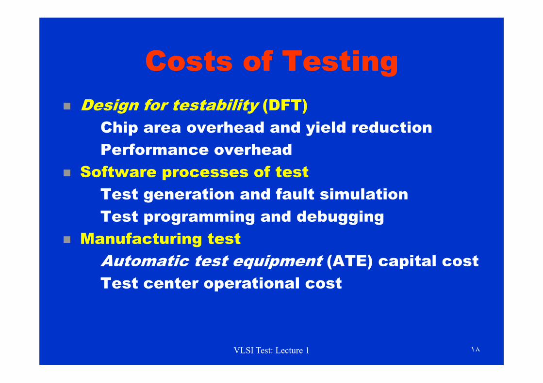
Costs of TestingCosts of Testing Design for testability (DFT)
Chip area overhead and yield reductionPerformance overhead
Software processes of testTest generation and fault simulationTest programming and debugging
Manufacturing testAutomatic test equipment (ATE) capital costTest center operational cost
VLSI Test: Lecture 1 ١٩
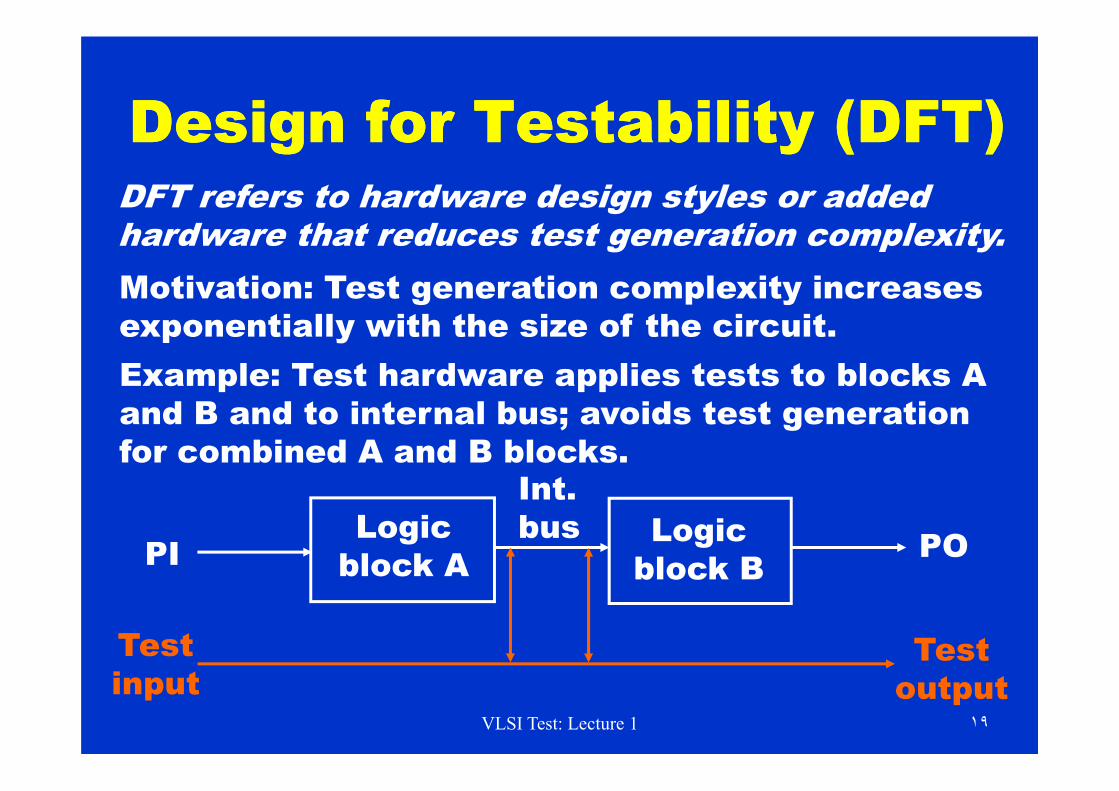
Design for Testability (DFT)Design for Testability (DFT)DFT refers to hardware design styles or addedhardware that reduces test generation complexity.Motivation: Test generation complexity increasesexponentially with the size of the circuit.
Logicblock A
Logicblock BPI PO
Testinput
Testoutput
Int.bus
Example: Test hardware applies tests to blocks Aand B and to internal bus; avoids test generationfor combined A and B blocks.
VLSI Test: Lecture 1 ٢٠
0.5
5
50
500
ICTest
BoardTest
SystemTest
WarrantyRepair
10
1
100
1000
Costperfault
(Dollars)
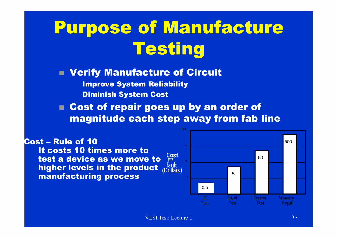
Purpose of Manufacture Testing
Purpose of Manufacture Testing
Verify Manufacture of CircuitImprove System ReliabilityDiminish System Cost
Cost of repair goes up by an order of magnitude each step away from fab line
Cost – Rule of 10It costs 10 times more to test a device as we move to higher levels in the product manufacturing process
VLSI Test: Lecture 1 ٢١
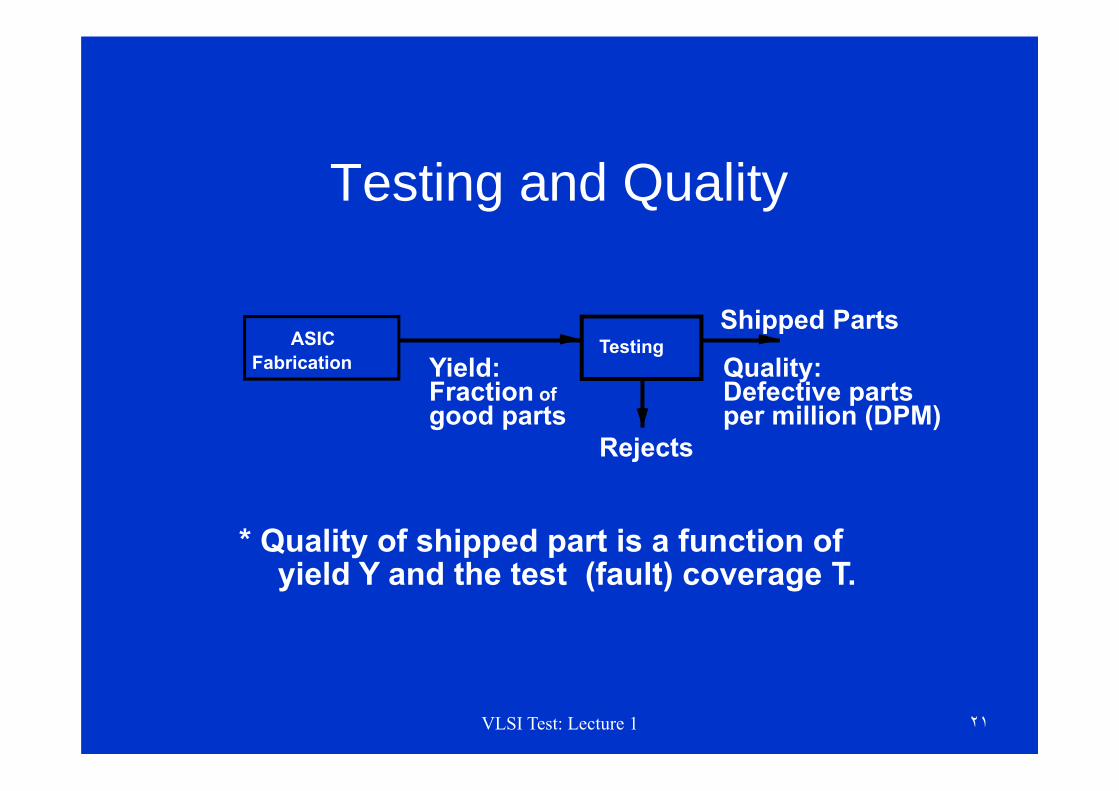
Testing and Quality
ASICFabrication
TestingYield:Fraction ofgood parts
Rejects
Shipped Parts
Quality:Defective partsper million (DPM)
* Quality of shipped part is a function ofyield Y and the test (fault) coverage T.
VLSI Test: Lecture 1 ٢٢
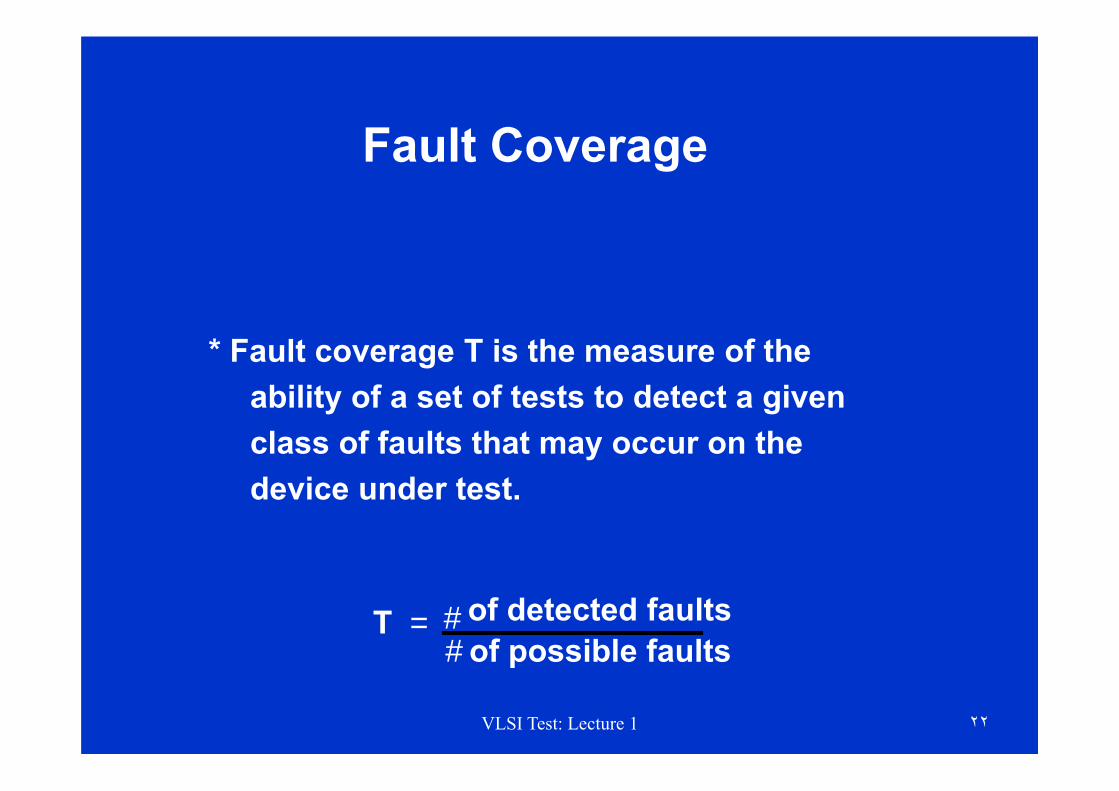
Fault Coverage
* Fault coverage T is the measure of theability of a set of tests to detect a givenclass of faults that may occur on thedevice under test.
T = # of detected faults# of possible faults
VLSI Test: Lecture 1 ٢٣
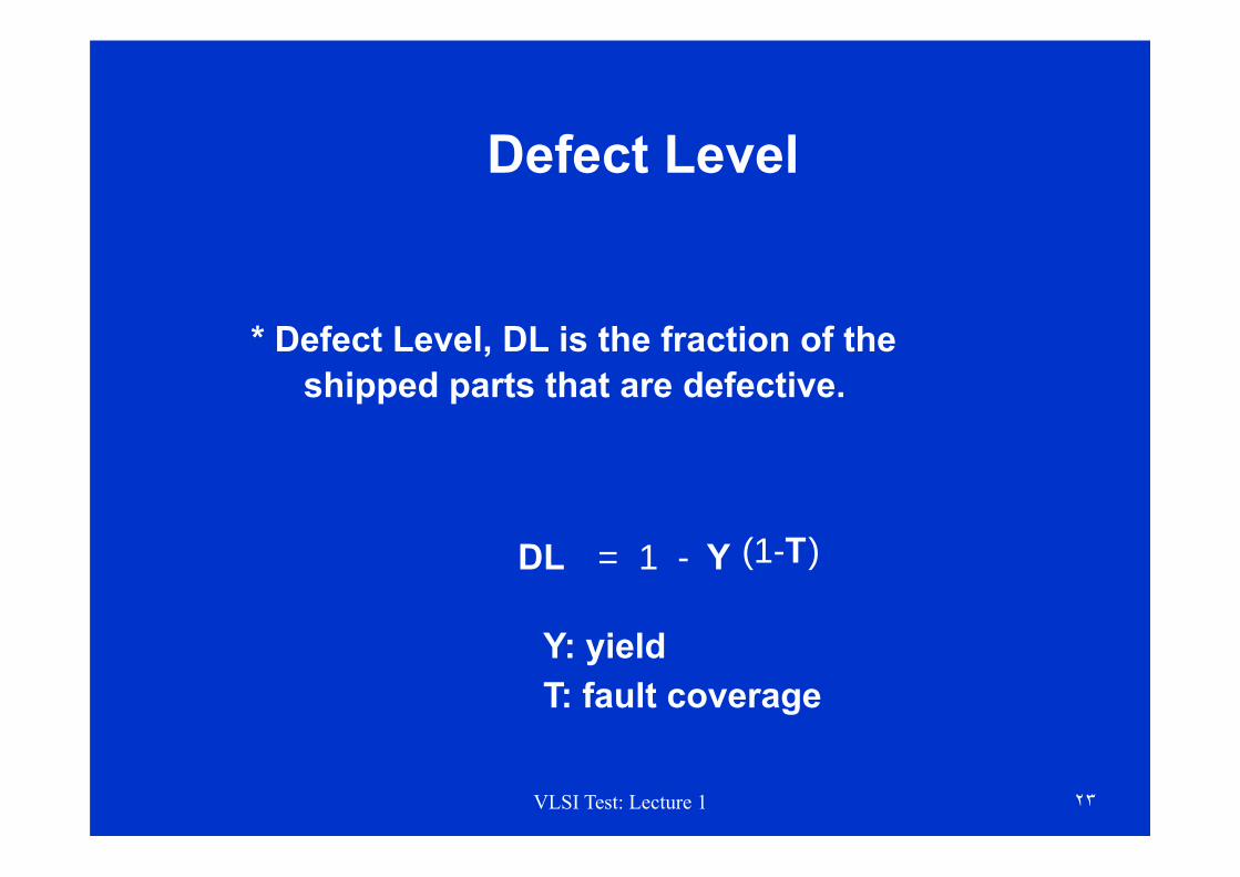
Defect Level
* Defect Level, DL is the fraction of theshipped parts that are defective.
DL = 1 - Y (1-T)
Y: yieldT: fault coverage

VLSI Test: Lecture 1 ٢٤
Relating Defect Level to Fault Coverage
0 10 20 30 40 50 60 70 80 90 1000
.1
.2
.3
.4
.5
.6
.7
.8
.9
1
Y=.99Y=.90
Y=.75
Y=.50
Y=.25
Y=.10
Y=.01
Y = Yield
Fault Coverage, T (%)
DL = 1 - Y(1-T)
VLSI Test: Lecture 1 ٢٥
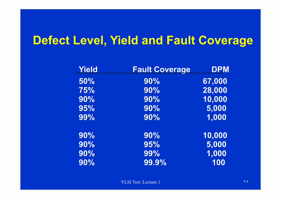
Defect Level, Yield and Fault Coverage
50% 90% 67,00075% 90% 28,00090% 90% 10,00095% 90% 5,00099% 90% 1,000
90% 90% 10,00090% 95% 5,00090% 99% 1,00090% 99.9% 100
Yield Fault Coverage DPM

VLSI Test: Lecture 23 ٢٦
Scan Flip-Flop (SFF)Scan Flip-Flop (SFF)D
TC
SD
CK
Q
QMUX
D flip-flop
Master latch Slave latch
Logicoverhead

VLSI Test: Lecture 23 ٢٧
Adding Scan StructureAdding Scan Structure
SFF
SFF
SFF
Combinational
logic
PI PO
SCANOUT
SCANINTC or TCK Not shown: CK or
MCK/SCK feed allSFFs.

Copyright 2001, Agrawal & Bushnell VLSI Test: Lecture 28 28
System Test LogicSystem Test Logic
Teat data Input
Serial Input to boundry register
Test ClockFor boundryScan
Test Mode Selet signal
AsyncronousReset For BoundryScan
Test Data Otput
Test acess port : finite state machine that recognizes the boundry scan communication protocol and controls the operation through internal signals

VLSI Test: Lecture 1 ٢٩
DFT Standards
IEEE Std. 1149.1
IEEE Std. 1149.1b
IEEE Std. 1149.5
IEEE Std. 1029.1
MIL-HDBK-XX47

VLSI Test: Lecture 1 ٣٠
IEEE Std. 1149.1 - Test Access Port and Boundary-
Scan Architecture
Defines the architecture of the TAP and Boundary Scan
cells
IEEE 1149.1b - defines the Boundary-Scan Description
Language (BSDL)
IEEE Std. P1149.2 - Extended Serial-Digital Interface
Standard
Defines a scheme that supports board-level
interconnect testing and internal-scan testing of
components
IEEE Std. P1149.3 - Real Time Test Bus Standard
Proposed to define standards for real-time testability
bus (work discontinued)

VLSI Test: Lecture 1 ٣١
IEEE Std. P1149.4 - Mixed-Signal Test Bus Standard
Proposed to extend the concept of boundary-scan to analog
and mixed signal devices
IEEE Std. P1149.5 - Module Test and Maintenance Bus
Standard
Defines specifications for a serial test and maintenance bus
for systems with two or more modules plugged into a
backplane
IEEE Std. 1029.1 - Waveform and Vector Exchange
Specification (WAVES)
Defines standard for VHDL description of stimulus vectors
and responses
MIL-HDBK-XX47 Testability Analysis Handbook
Defined the DoD view of Design for Test


VLSI Test: Lecture 1 ٣٣
Cost of Manufacturing Testing in 2000
Cost of Manufacturing Testing in 2000
0.5-1.0GHz, analog instruments,1,024 digital pins: ATE purchase price
= $1.2M + 1,024 x $3,000 = $4.272M Running cost (five-year linear depreciation)
= Depreciation + Maintenance + Operation= $0.854M + $0.085M + $0.5M= $1.439M/year
Test cost (24 hour ATE operation)= $1.439M/(365 x 24 x 3,600)= 4.5 cents/second

VLSI Test: Lecture 1 ٣٤
Roles of TestingRoles of Testing
Detection: Determination whether or not the device under test (DUT) has some fault.
Diagnosis: Identification of a specific fault that is present on DUT.
Device characterization: Determination and correction of errors in design and/or test procedure.
Failure mode analysis (FMA): Determination of manufacturing process errors that may have caused defects on the DUT.
VLSI Test: Lecture 1 ٣٥
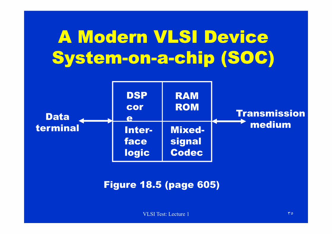
A Modern VLSI DeviceSystem-on-a-chip (SOC)A Modern VLSI Device
System-on-a-chip (SOC)
DSPcore
RAMROM
Inter-facelogic
Mixed-signalCodec
Dataterminal
Transmissionmedium
Figure 18.5 (page 605)

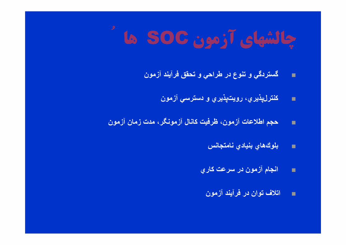
ها SOCچالشهاي آزمون ها SOCچالشهاي آزمون گستردگي و تنوع در طراحي و تحقق فرآيند آزمون
كنترل پذيري، رويت پذيري و دسترسي آزمون
حجم اطالعات آزمون، ظرفيت كانال آزمونگر، مدت زمان آزمون
بلوك ھاي بنيادي نامتجانس
انجام آزمون در سرعت كاري
اتالف توان در فرآيند آزمون