Embed Size (px)
Citation preview

VIN VOUT
R1/C1
ON/OFF
Q1
Q2
R1
C1
ESD ESD
ESD
ESD
R2
CL
(2, 3)
R2(1)
(5)
(6)
(4)
GPIO/Logic
Up to8V
SupplyLOAD
Product
Folder
Sample &Buy
Technical
Documents
Tools &
Software
Support &Community
TPS27081ASLVSBE9E –APRIL 2012–REVISED JUNE 2015
TPS27081A 1.2-V to 8-V, 3-A PFET High-Side Load SwitchWith Level Shift and Adjustable Slew Rate Control
1 Features 3 DescriptionThe TPS27081A device is a high-side load switch
1• Low ON-Resistance, High-Current PFETthat integrates a Power PFET and a Control NFET in– RDS(on) = 32 mΩ at VGS = –4.5 V a tiny package.
– RDS(on) = 44 mΩ at VGS = –3 VThe TPS27081A features industry-standard ESD
– RDS(on) = 82 mΩ at VGS = –1.8 V protection on all pins providing better ESD– RDS(on) = 93 mΩ at VGS = –1.5 V compatibility with other onboard components.– RDS(on) = 155 mΩ at VGS = –1.2 V The TPS27081A level shifts ON/OFF logic signal to
VIN levels and supports as low as 1-V CPU or MCU• Adjustable Turnon and Turnoff Slew Rate Controllogic to control higher voltage power supplies withoutThrough External R1, R2, and C1requiring an external level-shifter.• Supports a Wide Range of 1.2-V to 8-V Supply
Inputs Switching a large value output capacitor CL through afast ON/OFF logic signal may result in an excessive• Integrated NMOS for PFET Controlinrush current. To control the load inrush current,• NMOS ON/OFF Supports a Wide Range of 1-V to connect a resistor R2 and add an external capacitor
8-V Control Logic Interface C1 as shown in the Simplified Schematic. To• Full ESD Protection (All Pins) configure the TPS27081A to achieve a specific slew
rate, refer to the Application and Implementation– HBM 2 kV, CDM 500 Vsection.• Ultra-Low Leakage Current in Standby (TypicalA single pullup resistor R1 is required in standby100 nA)power switch applications. In such applications• Available in Tiny 6-Pin Packageconnect the R2 pin of the TPS27081A to the system
– 2.9 mm × 2.8 mm × 0.75 mm SOT (DDC) ground when inrush current control is not required.
2 Applications Device Information(1)
PART NUMBER PACKAGE BODY SIZE (NOM)• High-Side Load SwitchesTPS27081A SOT (6) 2.90 mm × 1.60 mm• Inrush Current Control(1) For all available packages, see the orderable addendum at• Power Sequencing and Control
the end of the data sheet.• Standby Power Isolation• Portable Power Switches
Simplified Schematic
1
An IMPORTANT NOTICE at the end of this data sheet addresses availability, warranty, changes, use in safety-critical applications,intellectual property matters and other important disclaimers. PRODUCTION DATA.

TPS27081ASLVSBE9E –APRIL 2012–REVISED JUNE 2015 www.ti.com
Table of Contents1 Features .................................................................. 1 8 Application and Implementation ........................ 10
8.1 Application Information............................................ 102 Applications ........................................................... 18.2 Typical Application ................................................. 103 Description ............................................................. 18.3 System Examples ................................................... 144 Revision History..................................................... 2
9 Power Supply Recommendations ...................... 175 Pin Configuration and Functions ......................... 310 Layout................................................................... 176 Specifications......................................................... 3
10.1 Layout Guidelines ................................................. 176.1 Absolute Maximum Ratings ...................................... 310.2 Layout Example .................................................... 176.2 ESD Ratings.............................................................. 410.3 Thermal Reliability................................................. 186.3 Recommended Operating Conditions....................... 410.4 Improving Package Thermal Performance ........... 186.4 Thermal Information .................................................. 4
11 Device and Documentation Support ................. 196.5 Electrical Characteristics........................................... 511.1 Community Resources.......................................... 196.6 Typical Characteristics .............................................. 611.2 Trademarks ........................................................... 197 Detailed Description .............................................. 911.3 Electrostatic Discharge Caution............................ 197.1 Overview ................................................................... 911.4 Glossary ................................................................ 197.2 Functional Block Diagram ......................................... 9
12 Mechanical, Packaging, and Orderable7.3 Feature Description................................................... 9Information ........................................................... 197.4 Device Functional Modes.......................................... 9
4 Revision HistoryNOTE: Page numbers for previous revisions may differ from page numbers in the current version.
Changes from Revision D (April 2013) to Revision E Page
• Added Pin Configuration and Functions section, ESD Ratings table, Feature Description section, Device FunctionalModes, Application and Implementation section, Power Supply Recommendations section, Layout section, Deviceand Documentation Support section, and Mechanical, Packaging, and Orderable Information section .............................. 1
Changes from Revision C (January 2013) to Revision D Page
• Updated wording in document................................................................................................................................................ 1
Changes from Revision B (September 2012) to Revision C Page
• Removed DRV package preview from datasheet. ................................................................................................................. 1
2 Submit Documentation Feedback Copyright © 2012–2015, Texas Instruments Incorporated
Product Folder Links: TPS27081A

R1/C1
ON/OFF
VIN
R2
VOUT
VOUT
1
2
3
6
5
4
TPS27081Awww.ti.com SLVSBE9E –APRIL 2012–REVISED JUNE 2015
5 Pin Configuration and Functions
DDC Package6-Pin SOTTop View
Pin FunctionsPIN
I/O (1) DESCRIPTIONNAME NO.
Active high enable. When driven with a high-impedance driver, connect an external pull down resistorON/OFF 5 I to GNDR1/C1 6 I Gate terminal of power PFET (Q1)
Source terminal of NMOS (Q2) . Connect to system GND directly or through a slew rate controlR2 1 O resistorVIN 4 I Source terminal of power PFET (Q1). Connect a pull-up resistor between the pins VIN/R1 and R1/C1
2VOUT O Drain terminal of power PFET (Q1). Connect a slew control capacitor between pins VOUT and R1/C1
3
(1) I = Input, O = Output
6 Specifications
6.1 Absolute Maximum RatingsSpecified at TJ = –40°C to 105°C unless otherwise noted. (1) (2)
MIN MAX UNITVIN(max) VIN pin maximum voltage with reference to pin R2 –0.1 8 VVOUT(max) VOUT pin maximum voltage with reference to pin R2 –0.1 8 VVON/OFF ON/OFF in maximum voltage with respect to pin R2 –0.3 8 V
Maximum continuous drain current of Q1 at TJ = 105°C 3IQ1(on) A
Maximum pulsed drain current of Q1 (3) at TJ = 105°C 9.5PD Maximum power dissipation at TA = 25°C, TJ = 150°C, RθJA = 105°C/W 1190 mWTA Operating free-air ambient temperature –40 85 (4) °CTJ(max)
(5) Operating virtual junction temperature 150 °CTstg Storage temperature –65 150 °C
(1) Stresses beyond those listed under Absolute Maximum Ratings may cause permanent damage to the device. These are stress ratingsonly, which do not imply functional operation of the device at these or any other conditions beyond those indicated under RecommendedOperating Conditions. Exposure to absolute-maximum-rated conditions for extended periods may affect device reliability.
(2) Refer to TI’s design support web page at www.ti.com/thermal for improving device thermal performance.(3) Pulse width <300 µs, duty cycle < 2%(4) TJ(max) limits and other related conditions apply. Refer to SOA charts, Figure 8 through Figure 12.(5) Operating at the absolute TJ(max) = 150°C can affect reliability. For higher reliability,TI recommends maintaining TJ < 105°C.
Copyright © 2012–2015, Texas Instruments Incorporated Submit Documentation Feedback 3
Product Folder Links: TPS27081A

TPS27081ASLVSBE9E –APRIL 2012–REVISED JUNE 2015 www.ti.com
6.2 ESD RatingsVALUE UNIT
Human body model (HBM), per ANSI/ESDA/JEDEC JS-001, all pins (1) ±2000ElectrostaticV(ESD) Vdischarge Charged device model (CDM), per JEDEC specification JESD22-C101, all pins (2) ±500
(1) JEDEC document JEP155 states that 500-V HBM allows safe manufacturing with a standard ESD control process.(2) JEDEC document JEP157 states that 250-V CDM allows safe manufacturing with a standard ESD control process.
6.3 Recommended Operating Conditionsover operating free-air temperature range (unless otherwise noted)
MIN NOM MAX UNITVIN Input voltage 1 8 VTA Operating free-air ambient temperature –40 85 °CTJ Junction temperature –40 105 °C
6.4 Thermal InformationTPS27081A
THERMAL METRIC (1) DDC (SOT) UNIT6 PINS
RθJA Junction-to-ambient thermal resistance 105 °C/WRθJC(top) Junction-to-case (top) thermal resistance 43 °C/WRθJB Junction-to-board thermal resistance 17.8 °C/WψJT Junction-to-top characterization parameter 6.5 °C/WψJB Junction-to-board characterization parameter 16.2 °C/WRθJC(bot) Junction-to-case (bottom) thermal resistance n/a °C/W
(1) For more information about traditional and new thermal metrics, see the Semiconductor and IC Package Thermal Metrics applicationreport, SPRA953.
4 Submit Documentation Feedback Copyright © 2012–2015, Texas Instruments Incorporated
Product Folder Links: TPS27081A

TPS27081Awww.ti.com SLVSBE9E –APRIL 2012–REVISED JUNE 2015
6.5 Electrical CharacteristicsSpecified over the recommended junction temperature range TJ = –40°C to 105°C unless otherwise noted. Typical valuesspecified at TA = TJ = 25°C.
PARAMETER TEST CONDITIONS MIN TYP MAX UNITOFF-TIME CHARACTERISTICS
Q1 drain-to-sourceBVIN1 VON/OFF = 0 V, VGS(Q1) = 0 V, ID(Q1) = 250 µA –8 Vbreakdown voltageTJ = 25°C 0.15 0.75
VIN = 8 V, VON/OFF = 0 V, RR1 = 10 kΩTJ = 85°C (2) 5 20VIN pin total leakageILOAD
(1) µAcurrent TJ = 25°C 0.05VIN = 5 V, VON/OFF = 0 V, RR1 = 10 kΩ
TJ = 85°C (2) 2TJ = 25°C 0.03 0.05
VIN = 8 V, VON/OFF = 0 V µATJ = 85°C (2) 0.35 0.6Q2 drain-to-sourceIFQ2 leakage current TJ = 25°C 0.025
VIN = 5 V, VON/OFF = 0 V µATJ = 85°C (2) 0.25
ON-TIME CHARACTERISTICS (3)
VIN = 5 V, ID(Q1) < 2 µA, RR1 = 10 kΩ, TJ = 25°C 0.3RR2 = RL = 0 ΩON/OFF pin low-levelVIL Vinput voltage VIN = 5 V, ID(Q1) < 20 µA, TJ = 85°C (2) 0.2RR1 = 10 kΩ, RR2 = RL = 0 ΩON/OFF pin high-VIH VIN = 5 V, RR1 = 10 kΩ 1 Vlevel input voltage
VGS = –4.5 V, ID(Q1) = 3 A 32 55VGS = –3 V, ID(Q1) = 2.5 A 44 77VGS = –2.5 V, ID(Q1) = 2.5 A 50 85Q1 Channel ON-RQ1(on) mΩresistance (4) VGS = –1.8 V, ID(Q1) = 2 A 82 147VGS = –1.5 V, ID(Q1) = 1 A 93 166VGS = –1.2 V, ID(Q1) = 0.5 A 155 260VGS = 4.5 V, ID(Q2) = 0.4 A 1.8 3VGS = 3.0 V, ID(Q2) = 0.3 A 2.3 6.2VGS = 2.5 V, ID(Q2) = 0.2 A 2.6 6.1Q2 Channel ON-RQ2(on) Ωresistance VGS = 1.8 V, ID(Q2) = 0.1 A 3.8 10VGS = 1.5 V, ID(Q2) = 0.05 A 4.4 8.5VGS = 1.2 V, ID(Q2) = 0.03 A 6.25 13.5
Q1 DRAIN-SOURCE DIODE PARAMETERS (3) (5)
Source-drain diodeIFSD VFSD = 0.8 V, VON/OFF = 0 V 1 Apeak forward currentSource-drain diodeVFSD VON/OFF = 0 V, IFSD = –0.6 A 1 Vforward voltage
(1) Pullup resistor (RR1) dependent.(2) Specified by design. Not production tested.(3) Pulse width < 300 µs, duty cycle < 2.0%(4) Refer to PFET Q1 Minimum Safe Operating Area (SOA) section for current rating.(5) Not rated for continuous current operation.
Copyright © 2012–2015, Texas Instruments Incorporated Submit Documentation Feedback 5
Product Folder Links: TPS27081A

0
0.03
0.06
0.09
0.12
0.15
0 0.5 1 1.5 2 2.5 3
Vdr
op (
V)
ILoad (A)
25 degC
85 degC
C003
0
0.03
0.06
0.09
0.12
0.15
0 0.5 1 1.5 2 2.5 3
Vdr
op (
V)
ILoad (A)
25 degC
85 degC
C003
0
0.04
0.08
0.12
0.16
0 0.5 1 1.5 2 2.5
Vdr
op (
V)
ILoad (A)
25 degC
85 degC
C003
0
0.03
0.06
0.09
0.12
0.15
0 0.5 1 1.5 2 2.5
Vdr
op (
V)
ILoad (A)
25 degC
85 degC
C003
0
0.025
0.05
0.075
0.1
0 0.1 0.2 0.3 0.4 0.5
Vdr
op (
V)
ILoad (A)
25 degC
85 degC
C001
0
0.05
0.1
0.15
0.2
0 0.5 1 1.5 2
Vdr
op (
V)
ILoad (A)
25 degC
85 degC
C003
TPS27081ASLVSBE9E –APRIL 2012–REVISED JUNE 2015 www.ti.com
6.6 Typical Characteristics
VGS(Q1) = –1.2 V VGS(Q1) = –1.8 V
Figure 1. Drop Voltage vs Load Current Figure 2. Drop Voltage vs Load Current
VGS(Q1) = –2.5 V VGS(Q1) = –3.3 V
Figure 3. Drop Voltage vs Load Current Figure 4. Drop Voltage vs Load Current
VGS(Q1) = –4.5 V VGS(Q1) = –5.5 V
Figure 5. Drop Voltage vs Load Current Figure 6. Drop Voltage vs Load Current
6 Submit Documentation Feedback Copyright © 2012–2015, Texas Instruments Incorporated
Product Folder Links: TPS27081A

0.00
0.50
1.00
1.50
2.00
2.50
3.00
0 20 40 60 80 100 120
Load
Cur
rent
(A
)
Ambient Temp (ºC)
Load Current (A)
C001
0.00
0.50
1.00
1.50
2.00
2.50
0 20 40 60 80 100 120
Load
Cur
rent
(A
)
Ambient Temp (ºC)
Load Current (A)
C001
0.00
0.50
1.00
1.50
2.00
2.50
3.00
3.50
0 20 40 60 80 100 120
Load
Cur
rent
(A
)
Ambient Temp C
Load Current (A)
C008
0.00
0.50
1.00
1.50
2.00
2.50
3.00
0 20 40 60 80 100 120
Load
Cur
rent
(A
)
Ambient Temp (ºC)
Load Current (A)
C001
0
0.03
0.06
0.09
0.12
0.15
0 0.5 1 1.5 2 2.5 3
Vdr
op (
V)
ILoad (A)
25 degC
85 degC
C003
0
0.03
0.06
0.09
0.12
0.15
0 0.5 1 1.5 2 2.5 3
Vdr
op (
V)
ILoad (A)
25 degC
85 degC
C003
TPS27081Awww.ti.com SLVSBE9E –APRIL 2012–REVISED JUNE 2015
Typical Characteristics (continued)
VGS(Q1) = –7 V Figure 0. UNDEFINED
Figure 7. Drop Voltage vs Load Current
6.6.1 PFET Q1 Minimum Safe Operating Area (SOA)
VGS_Q1 = –4.5 V VGS_Q1 = –3 V
Figure 8. Q1 Safe Operating Area Figure 9. Q1 Safe Operating Area
VGS_Q1 = –2.5 V VGS_Q1 = –1.8 V
Figure 10. Q1 Safe Operating Area Figure 11. Q1 Safe Operating Area
Copyright © 2012–2015, Texas Instruments Incorporated Submit Documentation Feedback 7
Product Folder Links: TPS27081A

0.00
0.10
0.20
0.30
0.40
0.50
0.60
0 20 40 60 80 100 120
Load
Cur
rent
(A
)
Ambient Temp C
Load Current (A)
C008
TPS27081ASLVSBE9E –APRIL 2012–REVISED JUNE 2015 www.ti.com
PFET Q1 Minimum Safe Operating Area (SOA) (continued)
VGS_Q1 = –1.2 V
Figure 12. Q1 Safe Operating Area
8 Submit Documentation Feedback Copyright © 2012–2015, Texas Instruments Incorporated
Product Folder Links: TPS27081A

R2
4
6
5
2
3
1
R1/C1
ON/OFF
VIN VOUT
VOUT
TPS27081Awww.ti.com SLVSBE9E –APRIL 2012–REVISED JUNE 2015
7 Detailed Description
7.1 OverviewThe TPS27081A device is a load switch capable fo handing up to 8 V and 3 A. To reduce voltage drop for lowvoltage and high current rails, the device implements an ultra-low resistance P-channel MOSFET which reducesthe dropout voltage through the device.
The device has a programmable slew rate which helps reduce or eliminate power supply droop due to largeinrush currents. During shutdown, the device has very low leakage currents.
7.2 Functional Block Diagram
7.3 Feature DescriptionThe TPS27081A device uses a low-voltage power PMOS transistor used as the pass element or switch betweenthe supply and load. The device also uses an NMOS transistor to turn the PMOS on and off by interfacing with awide range of GPIO voltages. Asserting an input voltage higher than VIH (1 V) enables the PMOS switch byturning the NMOS and the NMOS driving the PMOS gate towards ground. When using R2 to control output risetime and a pullup resistor R1 to tie the gate of the PMOS to the source to ensure turnoff, be sure to use an R1value big enough to source a small enough of current into R2 to not grossly effect the PMOS ON-state gatevoltage.
TPS27081A offers additional ports to control the output rise time by connecting passive elements between thesepins, VIN, and VOUT.
7.4 Device Functional Modes
7.4.1 ON/OFFWhen VIN > approximately 1 V and V(ON/OFF) > 1 V, the switch turns on and VOUT ≈ VIN.
When VIN > approximately 1 V and V(ON/OFF) <1 V, the switch turns off and VOUT ≠ VIN.
7.4.2 Fastest Output Rise TimeWhenever it is desired to achieve the fastest output rise time, tie pin 1 (R2) to ground and do not put a capacitorbetween VOUT (pins 2 and 3) and R1 and C1 (pin 6).
7.4.3 Controlled Output Rise TimeWhenever it is desired to control the output rise time, tie pin 1 (R2) to a resistance (R2) and put a capacitor (C1)between VOUT (pins 2 and 3) and R1 and C1 (pin 6). The values needed to determine a certain output rise timecan be determined by Equation 3.
Copyright © 2012–2015, Texas Instruments Incorporated Submit Documentation Feedback 9
Product Folder Links: TPS27081A

( )R1
GS(Q1) VINR1 R2
RV V (V)
R R= - ´
+
VIN VOUT
R1/C1
ON/OFF
Q1
Q2
R1
C1
ESD ESD
ESD
ESD
R2
CL
(2, 3)
R2(1)
(5)
(6)
(4)
GPIO/Logic
Up to8V
SupplyLOAD
TPS27081ASLVSBE9E –APRIL 2012–REVISED JUNE 2015 www.ti.com
8 Application and Implementation
NOTEInformation in the following applications sections is not part of the TI componentspecification, and TI does not warrant its accuracy or completeness. TI’s customers areresponsible for determining suitability of components for their purposes. Customers shouldvalidate and test their design implementation to confirm system functionality.
8.1 Application InformationThis section highlights some of the design considerations when implementing this device in various applications.
8.2 Typical Application
8.2.1 Standard Load Switching ApplicationThe TPS27081A device is a high-side load switch that integrates a power PFET and a control NMOS in a tinypackage. The device internal components are rated for up to 8-V supply and support up to 3 A of load current.The device can be used in a variety applications. Figure 13 shows a general application of the TPS27081Adevice to control the load inrush current.
Figure 13. Standard Application Diagram
8.2.1.1 Design Requirements
Table 1. Component TableCOMPONENT DESCRIPTION
R1 Level shift and pullup resistorR2 Optional (1)
C1 Optional (1)
(1) Required for load inrush current (slew rate) control.
8.2.1.2 Detailed Design Procedure
8.2.1.2.1 Configuring Q1 ON Resistance
The VGS(Q1) gate-to-source voltage across the PMOS transistor Q1 sets its ON-resistance RQ1(on). Directlyconnecting the pin R2 to ground maximizes the ON state VGS(Q1) and thus minimizes the VIN to VOUT voltagedropout. Equation 1 describes the VGS(Q1) when a resistor R2 is installed to control the turnon slew rate.
(1)
For example,when RR1 = 10 × RR2 and VVIN = 5 V, VGS(Q1) = –4.5 V
10 Submit Documentation Feedback Copyright © 2012–2015, Texas Instruments Incorporated
Product Folder Links: TPS27081A

( )
R2 C1RISE 2 3
VIN
3.9 R Ct (s)
V
´ ´=
OUT(final) OUT(initial)INRUSH LOAD LOAD
OUT(SR)
V VdvI C C
dt V
-
= ´ = ´
TPS27081Awww.ti.com SLVSBE9E –APRIL 2012–REVISED JUNE 2015
NOTETI recommends maintaining RR1 > 10 × RR2. The higher value of resistor R1 minimizesquiescent current when PMOS is on, however, the higher value may adversely impactOFF-state leakage current. Refer to the load current (ILOAD) specifications in the ElectricalCharacteristics table.
8.2.1.2.2 Configuring Turnon Slew Rate
Switching a large capacitive load CLOAD instantaneously results in a load inrush current given by Equation 2.
where• VOUT(SR) is the output voltage slew rate (2)
An uncontrolled fast rising ON/OFF logic input may result in a high slew rate at the output resulting in a very highdv/dt, thus, leading to a higher inrush current. To control the inrush current, connect a resistor R2 and a capacitorC1 as shown in Figure 13. Use the following equation to configure the TPS27081A slew rate to a specific value.Refer to Table 2 for component values to configure TPS27081A to achieve standard slew rates.
where• tRISE is the time delta starting from the rising edge of the ON/OFF signal to charge up the load capacitor CLOAD
from 10% to 90% of VIN voltage. (3)
NOTEEquation 3 is accurate to within ±20% across full VIN range supported by TPS27081A.Ensure that R1 > 10 × R2.
Table 2. Component Values for VOUT Rise TimeRISE TIME (µs) (1) (2)
RR1 = 10 kΩ, RR2 = 1 kΩ RR1 = 5.1 kΩ, RR2 = 510 ΩCC1 VVIN (V) VVIN (V)
7 5 3.3 1.2 7 5 3.3 1.2220 pF 0.253 0.316 0.416 0.810 0.129 0.161 0.212 0.4131000 pF 1.15 1.44 1.89 3.68 .586 .732 .963 1.884700 pF 5.4 6.75 8.88 17.3 2.76 3.44 4.53 8.830.18 µF 207 258 340 663 106 132 173 3380.27 µF 310 388 510 994 158 198 260 5070.33 µF 379 474 623 1220 194 242 318 620
1 µF 1150 1440 1890 3680 586 732 963 1880
(1) CLOAD = 10 µF. Output rise time is independent of CLOAD when CLOAD >> CC1.(2) Rise time is 250 ns for RR2 = 0 Ω and CC1 = CLOAD = 0 F.
8.2.1.2.3 Configuring Turnoff Delay
TPS27081A PMOS turnoff delay from the falling edge of ON/OFF logic signal depends upon the componentvalues of resistor R1 and capacitor C1. Lower values of resistor R1 ensures quicker turnoff.
toff > 2 × R1 × C1 sec (4)
Copyright © 2012–2015, Texas Instruments Incorporated Submit Documentation Feedback 11
Product Folder Links: TPS27081A

TPS27081ASLVSBE9E –APRIL 2012–REVISED JUNE 2015 www.ti.com
8.2.1.2.4 Low Voltage ON/OFF Interface
The VGS(Q2) is set by the ON/OFF logic level. To turn ON, the transistor Q2 requires a VGS > 1.0 V (typical). Forreliable operation, apply ON/OFF logic following the high-level input voltage (VIH) and low-level input voltage (VIL)limits expressed in Equation 5 and Equation 6.
VIH(on) > 1.0 V + IQ2 × R2 V (5)VIL(off) < 0.2 V (6)
Minimizing IQ2 × R2 drop helps achieve a direct interface with a low voltage ON/OFF logic. To minimize IQ2 × R2voltage drop, select a high R1 and R2 ratio. For example, when VVIN = 1.8 V, selecting R1 and R2 = 40 requiresVIH > 1 + 45 mV and thus allowing a 1.2-V GPIO interface.
In applications where ON/OFF signal is not available, connect ON/OFF pin to VIN. The TPS27081A turnsON/OFF in sync with the input supply connected to the VIN pin.
NOTEConnect a pulldown resistor between ON/OFF pin to GND when ON/OFF is driven by ahigh-impedance (tri-state) driver.
8.2.1.2.5 ON-Chip Power Dissipation
Use Equation 7 to calculate TPS27081A ON-chip power dissipation PD:PD = IDQ1
2 × RQ1(on) +IDQ22 × RQ2(on)
where• IDQ1 and IDQ2 are the DC current flowing through the transistors Q1 and Q2, respectively. (7)
Refer to Electrical Characteristics and/or Figure 1 through Figure 7 to estimate RQ1(on) and RQ2(on) for variousvalues of VGS(Q1) and VGS(Q2), respectively.
NOTEMOS switches can get extremely hot when operated in saturation region. As a generalguideline, to avoid transistors Q1 and Q2 going into saturation region, set VGS > VT +VDS. For example, VGS > 1.5 V and VDS < 200 mV ensures operation as a switch.
12 Submit Documentation Feedback Copyright © 2012–2015, Texas Instruments Incorporated
Product Folder Links: TPS27081A

Time (Ps)-50 0 50 100 150 200 250 300 350 400 450
-0.5
0
0.5
1
1.5
2
2.5
3
3.5
4
4.5
5
5.5
ICL (A)VOUT (V)VIN (V)
Time (Ps)-2 0 2 4 6 8 10 12 14 16 18
-0.5
0
0.5
1
1.5
2
2.5
3
3.5
4
4.5
5
5.5
ICL (A)VOUT (V)VIN (V)
Time (Ps)-5 0 5 10 15 20 25 30 35 40 45
-0.5
0
0.5
1
1.5
2
2.5
3
3.5
4
4.5
5
5.5
ICL (A)VOUT (V)VIN (V)
TPS27081Awww.ti.com SLVSBE9E –APRIL 2012–REVISED JUNE 2015
8.2.1.3 Application Curves
CC1 = 330 pF CC1 = 3300 pF
Figure 14. Output Rise Time and Inrush Current Figure 15. Output Rise Time and Inrush Current
CC1 = 33 nF
Figure 16. Output Rise Time and Inrush Current
Copyright © 2012–2015, Texas Instruments Incorporated Submit Documentation Feedback 13
Product Folder Links: TPS27081A

VIN VOUT
R1/C1
ON/OFF
Q1
Q2
R1CIN
(2, 3)
R2(1)
(5)
(6)
(4)1.8 - 8VInput
Boost Reg
CINVIN SW
FB
GPIO
SHDN
VIN VOUT
R1/C1
ON/OFF
Q1
Q2
R1COUT
(2, 3)
R2(1)
(5)
(6)
(4)
GPIO
Up to8V
Input CINVDD
StandbyModule
Always ONModules
VDD
TPS27081ASLVSBE9E –APRIL 2012–REVISED JUNE 2015 www.ti.com
8.3 System Examples
8.3.1 Standby Power IsolationMany applications have some always ON modules to support various core functions. However, some modulesare selectively powered ON or OFF to save power and multiplexing of various on board resources. Suchmodules that are selectively turned ON or OFF require standby power generation. In such applicationsTPS27081A requires only a single pull-up resistor. In the configuration shown in Figure 17, the VOUT voltagerise time is approximately 250 ns when VVIN = 5 V.
Figure 17. Standby Power Generation Using TPS27081A
8.3.2 Boost Regulator With True ShutdownThe most common boost regulator topology provides a current leakage path through inductor and diode into thefeedback resistor even when the regulator shuts down. Adding a TPS27081A device in the input-side power pathprevents this leakage current and thus providing a true shutdown, as shown in Figure 18.
LCD panels require inrush current control to prevent permanent system damages during turnon and turnoffevents.
Figure 18. True Shutdown Using TPS27081A
14 Submit Documentation Feedback Copyright © 2012–2015, Texas Instruments Incorporated
Product Folder Links: TPS27081A

VIN VOUT1
R1/C1
ON/OFF
Q1
Q2
R1
C1
R2
COUT1
(2, 3)
R2(1)
(5)
(6)
(4)
Module1
(CPU/MCU)
CINVDD1
1.2 - 8VInput VOUT2
R1/C1
ON/OFF
Q1
Q2
R3
C2
R4
COUT2
(2, 3)
R2(1)
(5)
(6)
(4)
Module2
VDD2
GPIO
LDO
SW Supply(DC-DC)
CPU/MCU/SOC
VIN VOUT1
R1/C1
ON/OFF
Q1
Q2
R1
C1
R2
CVDDIO
(2, 3)
R2(1)
(5)
(6)
(4)
CIN
VDDIO VDD
CVDD
DVDD
TPS27081Awww.ti.com SLVSBE9E –APRIL 2012–REVISED JUNE 2015
System Examples (continued)8.3.3 Single Module Multiple Power Supply SequencingMost modern SOCs and CPUs require multiple voltage inputs for its analog cores, digital cores, and I/Ointerfaces. These devices require that these supplies be applied simultaneously or in a certain sequence. TheTPS27081A device, when configured as shown in Figure 19 with the VOUT1 rise time adjusted appropriatelythrough resistor R2 and capacitor C1, delays the early arriving LDO output to match up with late-arriving DC-DCoutput and thus, achieving power sequencing.
Figure 19. Power Sequencing Using TPS27081A
8.3.4 Multiple Modules Interdependent Power Supply SequencingFor system integrity reasons, a certain power sequencing may be required among various modules. As shown inFigure 20, Module 2 powers up only after Module 1 is powered up and the Module 1 GPIO output is enabled toturn ON Module 2. The TPS27081A device, when used as shown in this example does not only sequence theModule 2 power, but it also helps prevent inrush current into the power path of Module 1 and 2.
Figure 20. Power Sequencing Using TPS27081A
Copyright © 2012–2015, Texas Instruments Incorporated Submit Documentation Feedback 15
Product Folder Links: TPS27081A

VIN VOUT
R1/C1
ON/OFF
Q1
Q2
R1
C1
R2
COUT1
(2, 3)
R2(1)
(5)
(6)
(4)
Module1
CINVDD1
Up to8V
Input
VOUT
R1/C1
ON/OFF
Q1
Q2
R3
C1
R4
COUT2
(2, 3)
R2(1)
(5)
(6)
(4)
Module2
VDD2
VIN VOUT
R1/C1
ON/OFF
Q1
Q2
R1
C1
R2
COUT
(2, 3)
R2(1)
(5)
(6)
(4)
GPIO
3-5VInput
TFTLCD
Module
CINVIN
TPS27081ASLVSBE9E –APRIL 2012–REVISED JUNE 2015 www.ti.com
System Examples (continued)8.3.5 TFT LCD Module Inrush Current ControlAs shown in Figure 21, LCD panels require inrush current control to prevent permanent system damages duringturnon and turnoff events.
Figure 21. Inrush Current Control Using TPS27081A
8.3.6 Multiple Modules Interdependent Supply Sequencing Without a GPIO InputWhen a GPIO signal is not available, connecting the ON/OFF pin of the TPS27081 device as connected toModule 2 powers up Module 2 after poweing up Module 1 when the values for resistor R4 and capacitor C1 arechosen appropriately. The two TPS27081A in this configuration as shown in Figure 22 can control load inrushcurrent.
Figure 22. Power Sequencing Using TPS27081A
16 Submit Documentation Feedback Copyright © 2012–2015, Texas Instruments Incorporated
Product Folder Links: TPS27081A

1
2
3 4
5
6R2
VOUT
VOUT
R1/C1
ON/OFF
VIN
TPS27081ADDC
VIA to Ground Plane
VOUT Bypass Capacitor
VIN Bypass Capacitor
R2
R1
C1
TPS27081Awww.ti.com SLVSBE9E –APRIL 2012–REVISED JUNE 2015
9 Power Supply RecommendationsThe device is designed to operate from a VIN range of 1 V to 8 V. This supply must be well regulated and placedas close to the device terminal as possible with the recommended 1-μF bypass capacitor. If the supply is locatedmore than a few inches from the device terminals, additional bulk capacitance may be required in addition to theceramic bypass capacitors. If additional bulk capacitance is required, an electrolytic, tantalum, or ceramiccapacitor of 1 μF may be sufficient.
10 Layout
10.1 Layout GuidelinesFor best operational performance of the device, use good PCB layout practices, including:• VIN and VOUT traces should be as short and wide as possible to accommodate for high current.• The VIN pin should be bypassed to ground with low ESR ceramic bypass capacitors. The typical
recommended bypass capacitance is 1-μF ceramic with X5R or X7R dielectric. This capacitor should beplaced as close to the device pins as possible.
• The VOUT pin should be bypassed to ground with low ESR ceramic bypass capacitors. The typicalrecommended bypass capacitance is one-tenth of the VIN bypass capacitor of X5R or X7R dielectric rating.This capacitor should be placed as close to the device pins as possible.
10.2 Layout Example
Figure 23. Layout Example
Copyright © 2012–2015, Texas Instruments Incorporated Submit Documentation Feedback 17
Product Folder Links: TPS27081A
( ) AJ max
MAX
JA
T T
PDRq
-=
TPS27081ASLVSBE9E –APRIL 2012–REVISED JUNE 2015 www.ti.com
10.3 Thermal ReliabilityFor higher reliability, TI recommends limiting the TPS27081A die junction temperature to less than 105°C. Thedevice junction temperature is directly proportional to the ON-chip power dissipation. Use the following equationto calculate maximum ON-chip power dissipation to achieve the maximum die junction temperature target:
where• TJ(max) is the target maximum junction temperature• TA is the operating ambient temperature• RθJA is the package junction to ambient thermal resistance (8)
10.4 Improving Package Thermal PerformanceThe package RθJA value under standard conditions on a High-K board is listed in . RθJA value depends on the PCboard layout. An external heat sink and/or a cooling mechanism, like a cold air fan, can help reduce RθJA andthus improve device thermal capabilities. Refer to TI’s design support web page at www.ti.com/thermal for ageneral guidance on improving device thermal performance.
18 Submit Documentation Feedback Copyright © 2012–2015, Texas Instruments Incorporated
Product Folder Links: TPS27081A

TPS27081Awww.ti.com SLVSBE9E –APRIL 2012–REVISED JUNE 2015
11 Device and Documentation Support
11.1 Community ResourcesThe following links connect to TI community resources. Linked contents are provided "AS IS" by the respectivecontributors. They do not constitute TI specifications and do not necessarily reflect TI's views; see TI's Terms ofUse.
TI E2E™ Online Community TI's Engineer-to-Engineer (E2E) Community. Created to foster collaborationamong engineers. At e2e.ti.com, you can ask questions, share knowledge, explore ideas and helpsolve problems with fellow engineers.
Design Support TI's Design Support Quickly find helpful E2E forums along with design support tools andcontact information for technical support.
11.2 TrademarksE2E is a trademark of Texas Instruments.All other trademarks are the property of their respective owners.
11.3 Electrostatic Discharge CautionThese devices have limited built-in ESD protection. The leads should be shorted together or the device placed in conductive foamduring storage or handling to prevent electrostatic damage to the MOS gates.
11.4 GlossarySLYZ022 — TI Glossary.
This glossary lists and explains terms, acronyms, and definitions.
12 Mechanical, Packaging, and Orderable InformationThe following pages include mechanical, packaging, and orderable information. This information is the mostcurrent data available for the designated devices. This data is subject to change without notice and revision ofthis document. For browser-based versions of this data sheet, refer to the left-hand navigation.
Copyright © 2012–2015, Texas Instruments Incorporated Submit Documentation Feedback 19
Product Folder Links: TPS27081A

PACKAGE OPTION ADDENDUM
www.ti.com 28-Feb-2017
Addendum-Page 1
PACKAGING INFORMATION
Orderable Device Status(1)
Package Type PackageDrawing
Pins PackageQty
Eco Plan(2)
Lead/Ball Finish(6)
MSL Peak Temp(3)
Op Temp (°C) Device Marking(4/5)
Samples
TPS27081ADDCR ACTIVE SOT-23-THIN DDC 6 3000 Green (RoHS& no Sb/Br)
CU SN Level-1-260C-UNLIM -40 to 85 AUA
(1) The marketing status values are defined as follows:ACTIVE: Product device recommended for new designs.LIFEBUY: TI has announced that the device will be discontinued, and a lifetime-buy period is in effect.NRND: Not recommended for new designs. Device is in production to support existing customers, but TI does not recommend using this part in a new design.PREVIEW: Device has been announced but is not in production. Samples may or may not be available.OBSOLETE: TI has discontinued the production of the device.
(2) Eco Plan - The planned eco-friendly classification: Pb-Free (RoHS), Pb-Free (RoHS Exempt), or Green (RoHS & no Sb/Br) - please check http://www.ti.com/productcontent for the latest availabilityinformation and additional product content details.TBD: The Pb-Free/Green conversion plan has not been defined.Pb-Free (RoHS): TI's terms "Lead-Free" or "Pb-Free" mean semiconductor products that are compatible with the current RoHS requirements for all 6 substances, including the requirement thatlead not exceed 0.1% by weight in homogeneous materials. Where designed to be soldered at high temperatures, TI Pb-Free products are suitable for use in specified lead-free processes.Pb-Free (RoHS Exempt): This component has a RoHS exemption for either 1) lead-based flip-chip solder bumps used between the die and package, or 2) lead-based die adhesive used betweenthe die and leadframe. The component is otherwise considered Pb-Free (RoHS compatible) as defined above.Green (RoHS & no Sb/Br): TI defines "Green" to mean Pb-Free (RoHS compatible), and free of Bromine (Br) and Antimony (Sb) based flame retardants (Br or Sb do not exceed 0.1% by weightin homogeneous material)
(3) MSL, Peak Temp. - The Moisture Sensitivity Level rating according to the JEDEC industry standard classifications, and peak solder temperature.
(4) There may be additional marking, which relates to the logo, the lot trace code information, or the environmental category on the device.
(5) Multiple Device Markings will be inside parentheses. Only one Device Marking contained in parentheses and separated by a "~" will appear on a device. If a line is indented then it is a continuationof the previous line and the two combined represent the entire Device Marking for that device.
(6) Lead/Ball Finish - Orderable Devices may have multiple material finish options. Finish options are separated by a vertical ruled line. Lead/Ball Finish values may wrap to two lines if the finishvalue exceeds the maximum column width.
Important Information and Disclaimer:The information provided on this page represents TI's knowledge and belief as of the date that it is provided. TI bases its knowledge and belief on informationprovided by third parties, and makes no representation or warranty as to the accuracy of such information. Efforts are underway to better integrate information from third parties. TI has taken andcontinues to take reasonable steps to provide representative and accurate information but may not have conducted destructive testing or chemical analysis on incoming materials and chemicals.TI and TI suppliers consider certain information to be proprietary, and thus CAS numbers and other limited information may not be available for release.
In no event shall TI's liability arising out of such information exceed the total purchase price of the TI part(s) at issue in this document sold by TI to Customer on an annual basis.

PACKAGE OPTION ADDENDUM
www.ti.com 28-Feb-2017
Addendum-Page 2

TAPE AND REEL INFORMATION
*All dimensions are nominal
Device PackageType
PackageDrawing
Pins SPQ ReelDiameter
(mm)
ReelWidth
W1 (mm)
A0(mm)
B0(mm)
K0(mm)
P1(mm)
W(mm)
Pin1Quadrant
TPS27081ADDCR SOT-23-THIN
DDC 6 3000 180.0 9.5 3.17 3.1 1.1 4.0 8.0 Q3
PACKAGE MATERIALS INFORMATION
www.ti.com 3-Mar-2017
Pack Materials-Page 1
*All dimensions are nominal
Device Package Type Package Drawing Pins SPQ Length (mm) Width (mm) Height (mm)
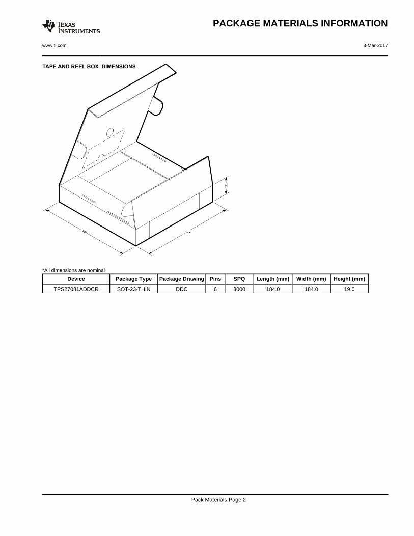
TPS27081ADDCR SOT-23-THIN DDC 6 3000 184.0 184.0 19.0
PACKAGE MATERIALS INFORMATION
www.ti.com 3-Mar-2017
Pack Materials-Page 2


IMPORTANT NOTICE
Texas Instruments Incorporated (TI) reserves the right to make corrections, enhancements, improvements and other changes to itssemiconductor products and services per JESD46, latest issue, and to discontinue any product or service per JESD48, latest issue. Buyersshould obtain the latest relevant information before placing orders and should verify that such information is current and complete.TI’s published terms of sale for semiconductor products (http://www.ti.com/sc/docs/stdterms.htm) apply to the sale of packaged integratedcircuit products that TI has qualified and released to market. Additional terms may apply to the use or sale of other types of TI products andservices.Reproduction of significant portions of TI information in TI data sheets is permissible only if reproduction is without alteration and isaccompanied by all associated warranties, conditions, limitations, and notices. TI is not responsible or liable for such reproduceddocumentation. Information of third parties may be subject to additional restrictions. Resale of TI products or services with statementsdifferent from or beyond the parameters stated by TI for that product or service voids all express and any implied warranties for theassociated TI product or service and is an unfair and deceptive business practice. TI is not responsible or liable for any such statements.Buyers and others who are developing systems that incorporate TI products (collectively, “Designers”) understand and agree that Designersremain responsible for using their independent analysis, evaluation and judgment in designing their applications and that Designers havefull and exclusive responsibility to assure the safety of Designers' applications and compliance of their applications (and of all TI productsused in or for Designers’ applications) with all applicable regulations, laws and other applicable requirements. Designer represents that, withrespect to their applications, Designer has all the necessary expertise to create and implement safeguards that (1) anticipate dangerousconsequences of failures, (2) monitor failures and their consequences, and (3) lessen the likelihood of failures that might cause harm andtake appropriate actions. Designer agrees that prior to using or distributing any applications that include TI products, Designer willthoroughly test such applications and the functionality of such TI products as used in such applications.TI’s provision of technical, application or other design advice, quality characterization, reliability data or other services or information,including, but not limited to, reference designs and materials relating to evaluation modules, (collectively, “TI Resources”) are intended toassist designers who are developing applications that incorporate TI products; by downloading, accessing or using TI Resources in anyway, Designer (individually or, if Designer is acting on behalf of a company, Designer’s company) agrees to use any particular TI Resourcesolely for this purpose and subject to the terms of this Notice.TI’s provision of TI Resources does not expand or otherwise alter TI’s applicable published warranties or warranty disclaimers for TIproducts, and no additional obligations or liabilities arise from TI providing such TI Resources. TI reserves the right to make corrections,enhancements, improvements and other changes to its TI Resources. TI has not conducted any testing other than that specificallydescribed in the published documentation for a particular TI Resource.Designer is authorized to use, copy and modify any individual TI Resource only in connection with the development of applications thatinclude the TI product(s) identified in such TI Resource. NO OTHER LICENSE, EXPRESS OR IMPLIED, BY ESTOPPEL OR OTHERWISETO ANY OTHER TI INTELLECTUAL PROPERTY RIGHT, AND NO LICENSE TO ANY TECHNOLOGY OR INTELLECTUAL PROPERTYRIGHT OF TI OR ANY THIRD PARTY IS GRANTED HEREIN, including but not limited to any patent right, copyright, mask work right, orother intellectual property right relating to any combination, machine, or process in which TI products or services are used. Informationregarding or referencing third-party products or services does not constitute a license to use such products or services, or a warranty orendorsement thereof. Use of TI Resources may require a license from a third party under the patents or other intellectual property of thethird party, or a license from TI under the patents or other intellectual property of TI.TI RESOURCES ARE PROVIDED “AS IS” AND WITH ALL FAULTS. TI DISCLAIMS ALL OTHER WARRANTIES ORREPRESENTATIONS, EXPRESS OR IMPLIED, REGARDING RESOURCES OR USE THEREOF, INCLUDING BUT NOT LIMITED TOACCURACY OR COMPLETENESS, TITLE, ANY EPIDEMIC FAILURE WARRANTY AND ANY IMPLIED WARRANTIES OFMERCHANTABILITY, FITNESS FOR A PARTICULAR PURPOSE, AND NON-INFRINGEMENT OF ANY THIRD PARTY INTELLECTUALPROPERTY RIGHTS. TI SHALL NOT BE LIABLE FOR AND SHALL NOT DEFEND OR INDEMNIFY DESIGNER AGAINST ANY CLAIM,INCLUDING BUT NOT LIMITED TO ANY INFRINGEMENT CLAIM THAT RELATES TO OR IS BASED ON ANY COMBINATION OFPRODUCTS EVEN IF DESCRIBED IN TI RESOURCES OR OTHERWISE. IN NO EVENT SHALL TI BE LIABLE FOR ANY ACTUAL,DIRECT, SPECIAL, COLLATERAL, INDIRECT, PUNITIVE, INCIDENTAL, CONSEQUENTIAL OR EXEMPLARY DAMAGES INCONNECTION WITH OR ARISING OUT OF TI RESOURCES OR USE THEREOF, AND REGARDLESS OF WHETHER TI HAS BEENADVISED OF THE POSSIBILITY OF SUCH DAMAGES.Unless TI has explicitly designated an individual product as meeting the requirements of a particular industry standard (e.g., ISO/TS 16949and ISO 26262), TI is not responsible for any failure to meet such industry standard requirements.Where TI specifically promotes products as facilitating functional safety or as compliant with industry functional safety standards, suchproducts are intended to help enable customers to design and create their own applications that meet applicable functional safety standardsand requirements. Using products in an application does not by itself establish any safety features in the application. Designers mustensure compliance with safety-related requirements and standards applicable to their applications. Designer may not use any TI products inlife-critical medical equipment unless authorized officers of the parties have executed a special contract specifically governing such use.Life-critical medical equipment is medical equipment where failure of such equipment would cause serious bodily injury or death (e.g., lifesupport, pacemakers, defibrillators, heart pumps, neurostimulators, and implantables). Such equipment includes, without limitation, allmedical devices identified by the U.S. Food and Drug Administration as Class III devices and equivalent classifications outside the U.S.TI may expressly designate certain products as completing a particular qualification (e.g., Q100, Military Grade, or Enhanced Product).Designers agree that it has the necessary expertise to select the product with the appropriate qualification designation for their applicationsand that proper product selection is at Designers’ own risk. Designers are solely responsible for compliance with all legal and regulatoryrequirements in connection with such selection.Designer will fully indemnify TI and its representatives against any damages, costs, losses, and/or liabilities arising out of Designer’s non-compliance with the terms and provisions of this Notice.
Mailing Address: Texas Instruments, Post Office Box 655303, Dallas, Texas 75265Copyright © 2017, Texas Instruments Incorporated
![Windows Mac OS X [10.8+] - Attasaattasa.com/madcatz/support/pdf/MCB32266-MUG-R2-10... · l2 l1 l2 r2 r2 r1 l2 l1 r1 l1 r2 r1 l2 l1 l2 r2 r1 l1 r2 r1 l2 l1 l2 r2.10.11. fcc id: p25d243710a4512c](https://img.pdfslide.net/doc/110x75/5ba4bf5f09d3f235188bed3d/windows-mac-os-x-108-l2-l1-l2-r2-r2-r1-l2-l1-r1-l1-r2-r1-l2-l1-l2-r2-r1.jpg)