Embed Size (px)
Citation preview

August, 31th, 2012
Compressive Sensing system
for recording of ECoG signals
in-vivo
- Master Thesis Project –
Mariazel Maqueda López
in fulfilment of the thesis requirements for the degree of
Master in Micro and Nanotechnologies
in a collaboration with
IMEC
supervised by
Prof. Alexandre Schmid
Mahsa Shoaran
Refet Firat Yazicioglu
Srinjoy Mitra

2

3
To my mother

4

5
The present project has been submitted to Grenoble INP - Phelma in
______________________ at the date of ______________________ by the student
Mariazel Maqueda López.
Sign of the student:
Sign of the Administration:

6

7
Acknowledgments
I would like to thank Prof. Alexandre Schmid, from EPFL, and Firat Refet Yazicioglu, from IMEC,
the great chance they have given to me by accepting my application to carry out the present
master thesis in both Microsystems Laboratory (LSM, EPFL) and Ultra Low Power and Extreme
Electronics group (ULPEXEL, IMEC).
It has been a challenge to settle in both, university and spin-off environments in such a short
period of time. As student I have learnt from some of the best professionals, but the experience
has extended to much more than the knowledge, because I have been included in two
wonderful groups of persons.
In the same way, I am immeasurably grateful for the help that Mahsa Shoaran and Srinjoy Mitra
have provided to me. Mahsa, thank you very much for the support and the good ideas. Srinjoy,
thank you for the patience and those useful feedbacks.
I am not allowed to forget Nikola Katic, Jie Zhang, Narasimha Venkata and Dhurv Chhetri for
our enlightening discussions, which have boosted me to evolve along these months of work.
Thanks to my family to be able to put up with the distance not only during the thesis period, if
not along these two long and short years of working hard in the Nanotech Master. Without your
unwavering support, all of these enriching months had not been possible. I specially has to
mention Jesús Maqueda Paniza, the new life was bloomed in between our large and loved
family, in some years you will understand that my heart was with you in the distance of your
short first steps.
Thanks to all of you, people from Leuven, to make the last episode of this adventure such an
incredible farewell.
Finally, I would like to particularly recognize the effort that Panagiota Morfouli, Fabrizio Pirri,
Suzanne Buffat and many more people have carried out to bring to fruition the seventh
generation of Nanotech Master students, there are not enough words to extol the wonderful
academic proposal that you have brought to us.

8

9
Abstract
The project “Compressive Sensing system for recording of ECoG signals in-vivo” has been
carried out as challenging collaboration between the Microelectronic System Laboratoy (LSM)
of the École Polytechnique Fédérale de Lausanne (EPFL, Switzerland) and the research
nanotechnology centre IMEC, (Leuven, Belgium). In this way, the context of the thesis has been
both, academic and industrially oriented. Regarding the latest ranking from Leiden University
has just been released at the end of 2011, and EPFL comes in at number twelve in the world
ranking and tops the table as the first non-American institution. EPFL and ETHZ, at 12th and
18th place respectively, rank as the top two non-American institutions. Considering IMEC, it has
built a research campus is headquartered in Leuven, but additional R&D teams in The
Netherlands, China, Taiwan, and India, and offices in Japan and the USA Belgium. It extends
over 24,400m² of office space, laboratories, training facilities, and technical support rooms,
including a 300nm and a 200mm cleanroom.
During the period which has taken place in EPFL, the motivation of the present project has
been, first of all, a deep study of the state of art of the new revealing methodology of signal
compression called Compressive Sensing. This phase has included mathematical basis to
accomplish compression, applicability scope and a wide range of different kind algorithms for
the signal recovery solution. In this way, models in Matlab and Simulink have been implemented
in order to apply an efficient compression and a reliable reconstruction.
In the last years, Compressive Sensing has emerged as a revolutionary compression technique
for sparse biological signals, which are becoming a high-dense source of information in
multielectrodes arrays-based bio-systems. Due to this fact, it has been studied how applying the
novel technique of Compressive Sensing in multichannel-multipath on-chip acquisition system
for the recording of Electrocorticography (ECoG) and Action Potentials (AP). ECoG and AP
neural signals have been proved to fit with the Compressive Sensing system requirements.
As a conclusion of the period in LSM, the publication “Circuit-Level Implementation of
Compressed Sensing for Multi-Channel Neural Recording” has been submitted as the first
reference about what has been called Spatial Compressive Sensing (SCS), a new method to
compress signals which are distributed over an array of multielectrodes and are sparse in the
spatial domain. Compressibility and reconstruction have been proved by different
implementations in Matlab and Cadence frames. In the same publication, a new, more compact
and parallel random generator system based on serial PRBSs has been submitted.
During the period in IMEC, a deepest study of the circuitry integration for Compressive Sensing
operation in neural signals has been accomplished. More specifically, a novel circuitry
implementation, for the mixing and integration of the incoming signals, has been proposed
according to an analog approach for the multipath topology.

10

11
Abstrait
Le projet " Compressive Sensing system for recording of ECoG signals in-vivo " a été réalisé
avec une collaboration de défi entre le Laboratoire des Systèmes Microélectroniques (LSM) de
l'Ecole Polytechnique Fédérale de Lausanne (EPFL, Suisse) et le centre de recherche en
nanotechnologie IMEC (Louvain, Belgique). Ainsi, la thèse a pu être abordée de manière à la fois
académique et industrielle. Dans le dernier classement publié à la fin 2011 par l'Université de
Leiden, l'EPFL arrive en douzième place et est en tête des universités non américaines. L'EPFL et
l'ETHZ, 12ème et 18ème respectivement, se classent comme les deux meilleurs institutions non
américaines. IMEC quant à lui est constitué d'un centre de recherche basé à Louvain, mais aussi
des équipes R&D aux Pays-Bas, en Chine, à Taiwan et en Inde, ainsi que des bureaux au Japon et
aux Etats-Unis. Le centre de Louvain s'étend sur 24.400m2 de bureaux, laboratoires, centres de
formation ainsi que de locaux de support technique dont des salles blanches de 300nm et 200mm.
Durant la période à l'EPFL, le but de ce projet était avant tout une étude approfondie sur la toute
nouvelle méthode de compression de signal appelée Compressive Sensing. Cette partie contenait
des bases mathématiques pour accomplir la compression, la fenêtre d'applicabilité et un large
éventail d'algorithmes pour la reconstitution du signal. Pour ce faire, des modèles Matlab et Simulink
ont été mis en place pour appliquer une compression efficace et une reconstruction fiable.
Ces dernières années, le Compressive Sensing a émérgé comme une technique de compression
révolutionnaire pour les signaux biologiques sparses, qui deviennent des sources importantes
d'information dans les bio-systèmes basés sur des rangées de microélectrodes. De ce fait, il a été
étudié comment cette nouvelle technique de Compressive Sensing dans des systèmes d'acquisition
multi-canal/multi-trajet on-chip pouvait être utilisée pour l'enregistrement d'Electrocorticographie
(ECoG) et de potentiels d'action (AP). Il a été montré que les signaux neuraux ECoG et AP étaient
compatibles avec les exigences des systèmes de Compressive Sensing.
En guise de conclusion de la période passée au LSM, l'article " Circuit-Level Implementation of
Compressed Sensing for Multi-Channel Neural Recording" a été soumis en tant que première
référence sur ce qu'on appelle le Spatial Compressive Sensing (SCS), une nouvelle méthode pour
compresser les signaux qui sont distribués sur une rangée de multiélectrodes et qui sont sparses
dans le domaine temporel. La compressibilité et la reconstruction ont été démontrée dans différentes
implémentations dans Matlab et Cadence. Dans ce même article, un nouveau générateur aléatoire,
plus compact et parallèle basé sur des PRBS en série a été développé.
Durant la période à IMEC, une étude plus approfondie de l'intégration des circuits de détection pour
la compression de signaux neuronaux a été accomplie. Plus précisément, un nouveau circuit pour le
mélange et l'intégration des signaux entrants a été proposé selon une approche analogue à la
topologie multi-trajet.

12

13
Riassunto
Il progetto “Compressive Sensing system for recording of ECoG signals in-vivo” è stato
realizzato attraverso una stimolante collaborazione tra il Microelectronic System Laboratory (LSM)
dell'École Polytechnique Fédérale de Lausanne (EPFL, Svizzera) e il centro di ricerca sulla micro e
nanotecnologia, IMEC, (Leuven, Belgio). In questo modo, il contesto della tesi è stato sia,
accademico che industriale. Per quanto riguarda l'ultima classifica dell'Università di Leiden alla fine
del 2011, l’EPFL arriva al numero dodici della classifica mondiale e in cima alla tabella come la prima
istituzione non americana. EPFL e ETHZ, al 12° e 18° posto, rispettivamente, sono le due prime
istituzione non americane. Per quel che riguarda IMEC, si tratta di un campus di ricerca con sede a
Lovanio, ma ha sedi distaccate nei Paesi Bassi, Cina, Taiwan e India, e uffici in Giappone e negli
Stati Uniti in Belgio. Si estende su 24.400 m² di spazio per uffici, laboratori, strutture di formazione e
sale di supporto tecnico, tra cui ci sono due cleanroom di 300 nm e 200mm.
Durante il periodo trascorso preso l’EPFL, la motivazione del presente progetto è stata, prima di
tutto, uno studio approfondito dello stato dell’arte della nuova metodologia di compressione dei
segnali chiamato Compressive Sensing. In questa fase, sono state studiate le base matematiche per
realizzare la compressione, l’applicabilità del metodo e una vasta gamma di algoritmi per la
soluzione del recupero dei segnali. In questo modo, sono stati svilupatti dei modelli in Matlab e
Simulink per applicare una compressione efficace e una ricostruzione affidabile.
Compressive Sensing è diventata una tecnica di compressione rivoluzionaria per i segnali biologici
classificati come sparsi, densa fonte di informazioni in biosistemi di multielettrodi. Per tanto, in questo
progetto è stato studiato come applicare la nuova tecnica Compressive Sensing in un sistema
multicanale on-chip orientato all’acquisizione di Electrocorticografia (ECoG) e Potenziali di Azione
(AP). I segnali neurali ECOG e AP hanno dimostrato di adattarsi ai requisiti del Compressive
Sensing.
Come conclusione del periodo di LSM, la pubblicazione “Circuit-Level Implementation of
Compressed Sensing for Multi-Channel Neural Recording” è stata presentata come il primo
riferimento dello Spatial Compressive Sensing (SCS), un nuovo metodo per la compressione dei
segnali che sono distribuiti su un array di multielettrodi e sono sparsi nel dominio spaziale. La
possibilita di comprimere e ricostruire questi segnali è stata dimostrata mediante implementazioni in
Matlab e Cadence. Nella stessa pubblicazione, un nuovo e più compatto generatore causale
parallelo basato in PRBS seriale è stato presentato.
Durante il periodo in IMEC, un più profondo studio della integrazione dei circuiti per
l’implemenntazione de un sistema basato in Compressive Sensing per l’applicazione in segnali
neurali è stato realizzato. Più in dettaglio, una nueva implementazione dei blocchi necessari per
effettuare il mixing e l'integrazione dei segnali in ingresso è stato proposto secondo un approccio
analogico per la topologia di multipath.

14

Gantt’s Chart
Notes: Red indications mean interleaved tasks. Green indications mean a finished tasks flow. Yellow indications mean EPFL-IMEC meetings.


17
Index
Acknowledgments 7
Abstract 9
Gannt’s Chart 15
1. Introduction: Framework for Compressive Sensing 25
2. State of the art 29
2.1. Neural Signals: EEG, ECoG and AP 29
2.2. Neural Signal Acquisition Systems On-Chip 30
2.3. Data Compression Methods 32
2.4. Compressive Sensing 33
2.4.1. Compressive sensing in a nutshell 33
2.4.2. Sparsifying bases 35
2.5. Reconstruction Methods 35
3. ECoG and AP Compressive Sensing System Design 37
3.1. Power Consumption Analysis 37
3.2. Single and Multi Channel Approach 38
4. Random Matrix Generation 39
4.1. Digital Implementation: Pseudo Random Binary Sequence (PRBS) 39
4.1.1. Basics of PRB: Serial and Parallel Implementation 39
4.1.2. Flips-Flops: Power and Area Analysis 42
4.1.3. Serial Implementation with two PRBS 43
4.1.4. Randomness Checking 45
5. System Level Design 47
5.1. Matlab and Simulink Models 47
5.2. Multi-Channel Implementation of Compressive Sensing 50
5.3. Reconstruction Method Application 52

18
5.3.1. Basis Pursuit Denoising Method (BPDM) 52
5.3.2. Least Absolute Shrinkage and Selection Operator (LASSO) 53
6. Analog Path Design 54
6.1. Design Discussion 54
6.2. Mixing and Integration 55
6.2.1. Passive Integration 55
6.2.2. Ideal Active Inverting Integration 58
6.2.3. DC-Offset Controlled Active Integration 61
6.2.4. Switched-Capacitor Integrator with parasitic effects 63
6.2.5. Non inverting SC Integrator without parasitic effects 66
6.2.6. SNR Calculations 68
7. Conclusions 71
7.1. Remarks 71
7.2. Next steps 72
Appendix 73
Appendix A 73
Appendix B 75
B.1. Digital Implementation 75
B.2. Analog Implementation 76
B.2.1. Current Mode 76
B.2.2. Voltage Mode 77
B.2.3. Charge Mode 79
Appendix C 81
C.1. Analog Implementation 81
C.1.1. Direct Amplification of Noise 81
C.1.2. High-Frequency Oscillator Sampling 81
Appendix D 83
Appendix E 84
E.1. Amplification 84

19
E.2. Signal Digital Conversion 84
Glossary 87
References 89

20
Index of Images
Figure 1.1. Energy a power costs for a typical biosensor configuration 26
Figure 1.2. Integrated Neural Interface (INI) 26
Figure 1.3. Characteristic Action Potential signal. 27
Figure 2.2.1. Example of wireless neural recording system 31
Figure 2.3.1. Transmission and Reception schemes in CS 32
Figure 2.4.1.1. Sketch of Compressive Sensing operation 34
Figure 2.4.2.1. Tree structure of 3-level decomposed wavelet coefficients 35
Figure 2.5.1. l1-minimization approaches to l0-minimization approach 36
Figure 3.4.1. Analog implementation proposal for neural acquisition channel 38
Figure 4.1.1.1. LSFR parallel (top) and serial (bottom) architectures 41
Figure 4.1.1.2. Galois (top) and Fibonacci (bottom) configurations 41
Figure 4.1.2.1. Reset-based Flip-Flop 42
Figure 4.1.2.2. TSPC Flip.Flop 42
Figure 4.1.3.1.Random Generator 43
Figure 4.1.3.2. Serial Implementation with two PRBS (4-FF and 5-FF) 44
Figure 4.2.3.3. Random states propagation by columns to the measurement matrix 44
Figure 5.1.1. Simulink implementation of a path 48
Figure 5.1.2. Details of the CS operation blocks for a path. 48
Figure 5.1.3. Compressed signal comparison 49
Figure 5.1.4. LASSO method reconstruction comparison 49
Figure 5.1.5. BPDN method reconstruction comparison 50
Figure 5.2.1. Spatial CS example 51
Figure 5.2.2. Original and reconstructed signal by applying SCS 52
Figure 6.5.1.1. Mixer and passive integrator circuitry 53

21
Figure 6.2.1.2. Input signal Spectra 56
Figure 6.2.1.3. Compressed signals comparison 57
Figure 6.2.1.4. LASSO reconstruction comparison 58
Figure 6.2.1.5. BPDN method reconstruction comparison 58
Figure 6.2.2.1. Mixer and ideal active inverting integrator circuitry 59
Figure 6.2.2.2. Ideal amplifier 59
Figure 6.2.2.3. Compressed signals comparison 60
Figure 6.2.2.4. LASSO reconstruction comparison 60
Figure 6.2.2.5. BPDN method reconstruction comparison 61
Figure 6.2.3.1. Modified active integrator 61
Figure 6.2.3.2. Compressed signal comparison 62
Figure 6.2.3.3. LASSO method reconstruction comparison 63
Figure 6.2.3.4. BPDN method reconstruction comparison 63
Figure 6.2.4.1. Switched-Capacitor Integrator with parasitic effect 64
Figure 6.2.4.2. Compressed signal comparison 65
Figure 6.2.4.3. LASSO method reconstruction comparison 65
Figure 6.2.4.4. BPDN method reconstruction comparison 66
Figure 6.2.5.1. Switched-Capacitor Integrator without parasitic effects 66
Figure 6.2.5.1. Compressed signal comparison 67
Figure 6.2.5.2. LASSO method reconstruction comparison 67
Figure 6.2.5.3. BPDN method reconstruction comparison 68
Figure B.1.1 Block diagram for a digital implementation of one CS channel 75
Figure B.1.2. Power consumption versus bandwidth for the digital implementation 76
Figure B.2.1.1. Circuit implementation of the proposed CS receiver 77
Figure B.2.2.1. Block diagram for an analog implementation 78
Figure B.2.2.2. Power consumption versus bandwidth for the analog implementation 78

22
Figure B.2.3.1. Switched Capacitor circuit implementation of the CS ADC 79
Figure B.2.3.2. Binary-weighted SC MDAC/summer for CS 80
Figure C.1.1.1. Random generator based on direct amplification of noise 81
Figure C.1.2.1. Basic oscillator-based TRNG 82
Figure E.2.1. Several techniques to digitize different kind of neural signals 85

23
Index of Tables
Table 2.1.1. Summary of main Neural Signals 30
Table 5.1. Main parameters of the CS analog design 47
Table 6.2.1.1. Main parameters for the simulation of the Passive Integrator-based multipath channel 56
Table 6.2.4.1. Main parameters for the simulation of the SC Integrator-based multipath channel 64
Table 6.2.6.1. SNR comparison between topologies and reconstruction methods 69
Table A.1. Main Reconstruction Methods 73
Table B.1.1. CS model specifications 75
Table B.2.1.1. CS model specifications 77
Table D.1. Selected crosses for 16 outputs through a 4FF-PRBS and a 5FF-PRBS 83
Table E.1.1. Main features of a front-end amplifier for neural recording 84

24

25
1. Introduction: Framework for Compressive Sensing
In many applications, including imaging systems, high-speed analog to digital converters, home
automation, environmental and medical monitoring and real-time diagnosis devices, data
compression turns in an indispensable requirement due to the large amount of information that
has to be integrated preferably in a low cost, low power and compact way. The technique called
Compressive Sensing has recently emerged as a compression method which easily enables the
integration on-chip of the compression algorithm, prosecuting a local signal processing in-situ.
Nowadays, in the case of biosignal-based systems, the number of sensor nodes rises up
according to the high dense integration phase of the CMOS technologies, so an increasing of
energy efficiency is essential to the continued development of the biomedical applications [1].
As it is shown in Chapter 2, data reduction firstly means a decreasing in the measurements to
be transmitted, which gives rise to a saving in power and area from the point of view of the
necessary processing devices, and secondly due to the fact that by employing a robust
compression technique the true signal information can eventually be better differentiated from
artifacts during signal recovery.
Among all the applications have been mentioned above, in particular, medical monitoring has
revealed as a challenging field of compression methods application due to the increasing
necessity of more implantable sensor nodes based on wireless technologies to achieve reliable
medical information. That translates into a higher integration of sensors in the same available
area, which have to consume as little power as possible in order to minimize the numbers of
times in which the power supplying batteries have to replaced, and so reducing costly surgeries
and improving the quality of life of patients. This kind of sensors is included within the Wireless
Body Sensor Network (WBSN) or Body Area Network (BAN) nodes that are intended for
personal health monitoring and assisted living, but also branch into lifestyle, sports and
entertainment applications [2].
As it has been introduced above, BAN systems are based on ultra-low power consumption
tendency in order to increase the energy autonomy of the devices. Nonetheless, BANs generate
large data rates which intrinsically imply an increasing in the power consumption relates to the
amplification, conversion, processing and over all, transmission of the information. Therefore,
medical monitoring based on BAN devices is an emerging application area which perfectly
exemplifies a scenario to apply integrated data compression.
In Fig.1.1, it is shown the energy and power costs for a typical wireless biosensor [3]. It is clear
that the transmitter results in an energy cost of approximately 1nJ/bit, much more than any
other component of the acquisition system, hence a data reduction approach should be taken
into consideration in order to minimize the energy cost of the system and maximize the data
throughput.

26
Figure 1.1. Energy a power costs for a typical biosensor configuration [4, 5, 6 7, 8].
In applications such an implantable neural recording arrays, as the number of microelectrode
within the arrays have increased in order to simultaneously understand the dynamics of many
neurons at almost single neuron scale, the data reduction becomes mandatory in order to be
able to transmit the recorded data. As a matter of fact, in recent years the advance in the
development of multichannels microprobes, for recording neural activity, has supposed a
significant milestone towards integrated microimplanted wireless devices for clinical applications
in the study of chronic illness, such as epilepsy.
In Fig.1.2 it is depicted an example of an array for neural data acquisition which has been
developed by researchers from the University of Utah [9]. It is possible to observe the
integration density of the platinum-tipped silicon microelectrodes over a volume of 4 x 4 x 1.5
mm3, which have been implemented in a matrix of 10 x 10 microelectrodes. It has to be taken
into consideration that independently from the resolution, when multielectrodes are placed in the
brain it is common for some electrodes to detect spikes from several distinct neurons while
other electrodes may see no resolvable spikes.
Figure 1.2. Integrated Neural Interface (INI) developed by University of Utah [9]. The 10 x 10
microelectode array has been implemented with an inter-probe distance of 400μm.
Neural signals acquisition systems, as ECoG and Action Potentials (AP), play a challenging role
in the biomedical applications development which has been introduced along this chapter
because of the saving in area and power which have to be mandatorily achieved in order to
implant the chips in human brains.
27
The final target is to reliably record as many data as possible, which will define the number of
channels, by keeping, as far as possible, the time and amplitude features of the signals. This
will state the processing and data transmission, so accordingly, data reduction becomes a
critical point in the design.
As it is shown in Chapter 3, numerous strategies for implementing integrated data compression
based on filtering have been developed to record neural spike events. However these solutions
initially exhibit less reliability to the entire feature extraction because information loss can take
place due to amplitude or time thresholds choices, and hence, there is a strict trade-off to be
respected between data reduction, robustness and implementation cost.
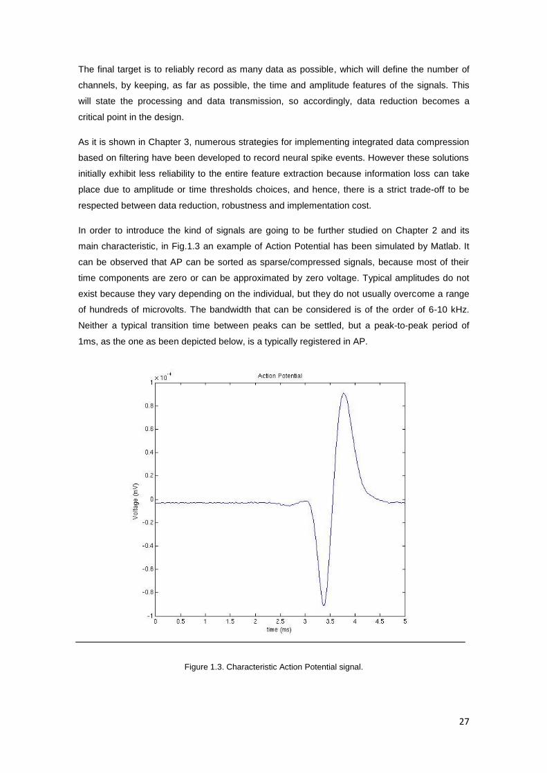
In order to introduce the kind of signals are going to be further studied on Chapter 2 and its
main characteristic, in Fig.1.3 an example of Action Potential has been simulated by Matlab. It
can be observed that AP can be sorted as sparse/compressed signals, because most of their
time components are zero or can be approximated by zero voltage. Typical amplitudes do not
exist because they vary depending on the individual, but they do not usually overcome a range
of hundreds of microvolts. The bandwidth that can be considered is of the order of 6-10 kHz.
Neither a typical transition time between peaks can be settled, but a peak-to-peak period of
1ms, as the one as been depicted below, is a typically registered in AP.
Figure 1.3. Characteristic Action Potential signal.

28

29
2. State of the art
2.1 Neural Signals: EEG, ECoG and AP [10]
A neuron is a cell which transmits bioelectrical information by both an electrical and chemical
signalling. All neurons are connected between each others in a neural network which
compounds the brain, spinal cord and peripheral ganglia. The electrical information that is
produced in the neurons is object of study in order to better understand neural diseases as
Alzheimer’s, Parkinson’s or epilepsy.
The different biopotentials that can be registered from the neurons enclose different kind of
information. The extracellular Action Potentials (AP) are generated with the depolarisation of the
membrane of a neuron, they have a frequency range between 100 Hz and 10 kHz in a duration
of few milliseconds and can occur from 10 to 120 times per second. The typical range of
amplitudes goes from 50 μV to 500 μV.
The Electroencephalogram (EEG) consists of the electrical activity resulting from ionic current
flows within the neurons. Its frequency varies between 1 mHz to 200 Hz, and its amplitude
between 1 to 10 mV. Diagnostic applications generally focus on the type of oscillations that can
be observed in EEG signals. In neurology, the main diagnostic application of EEG is in the case
of epilepsy, because epileptic activity can create clear abnormalities on a standard EEG study.
EEG is a key clinical diagnosis and monitoring tool that is frequently used in Brain-Computer
Interfaces (BCI).
Because the cerebrospinal fluid (CSF) of the brain as well as the skull and scalp cause a
smearing of the recorded electrical potential signals, an intracranial EEG is needed to recovery
brain activity [4]. The Electrocorticogram (ECoG) of subdural EEG signals are biopotentials
which are measured directly from the surface of the brain with a grid of electrodes implanted
under the skull.
Although signals measured with EEG and ECoG stem from the same activation in the brain,
there are several differences between them, ECoG has higher amplitude, a broader bandwidth,
a higher spatial resolution and is less vulnerable to artifacts so it present a better Signal-to-
Noise Ratio (SNR). These differences are mainly due to the fact that, in order to reach the scalp
electrodes of an EEG, electrical signals must also be conducted through the skull, where
potentials rapidly attenuate due to the low conductivity of bone. Due to all of these advantages
over EEG signals, BCI industry is rapidly moving toward this recording alternative.
A summary of the most relevant neural biopotentials has been included in Table 2.1.1.

30
Signal Amplitude Bandwidth
AP 50 to 500 μV 100 Hz to 10 kHz
Local Field
Potentials (LFP) 0.5 to 5 mV 2 mHz to 200 Hz
EEG 1 to 10 mV 1 mHz to 200 Hz
Ionic Current 1 to 10nA 1 mHz to 10 kHz
Redox Current 100 fA to 10 μA 1 mHz to 100 Hz (amperometry)
1 mHz to 10 kHz (FSCV)
Table 2.1.1. Summary of main Neural Signals.
2.2. Neural Signal Acquisition Systems On-Chip [10]
Nowadays, there is an intense development in neuroscience research which is aimed at the
development of new biomedical applications. This clinical target has resulted in the necessary
demand for neural interfacing microsystems capable of monitoring the activity of large groups of
neurons. Such devices are mainly composed of multiple neural probes, functionalized to
capture brain signals, which are connected to multiple processing channels able to extract and
transfer the neural data outside of the brain.
As it is submitted in Chapter 1, the two main aims of a neural signal acquisition system is
addressed to minimize area and power requirements, as well as to achieve the largest possible
resolution. An important point to be taken into consideration during the neural recording is the
existing interface capacitance which exists in the contact between metal electrode tip and the
neural tissue. The capacitance of the interface depends on the electrode area and surface
roughness, being values between 150 pF and 1.5 nF the common range of variation.
These emerging tools can be sorted into two main classifications, the systems which are
oriented to the extraction of relevant neural signals in order to establish a direct interaction
between an individual, who comes under a severe disability, and a computer or prostheses,
these applications are called Brain-Computer Interfaces (BCI). The other possible application
are those based on recording neural signals in order to subsequently be analyzed, in order to
shed some light about chronic neural diseases, as epilepsy.
During the last sixty years, the Central Nervous System (CNS) has been object of a prolific
research. In 1952, the experiments of Hodgkin and Huxley [11], gave rise into a precise model
of the generation of action potentials by neurons. Respectively, in 1957 and 1959, Mountcastle
[12] and Hubel [13] established a precise understanding of the visual cortex. In 1986,
Georgopoulos [14] probed the correlation between neural populations and movement directions
which led to the experimentation with non-human primates in order to study their motor cortex

31
patterns in response to visual targets in a three-dimensional space [15]. Several examples of
applications based on neuroprosthetic devices are Taylor [16] and Hochberg [17].
In the last years, microelectronics and microfabrication techniques have improved the
interfacing between individuals and analysing/actuation tools by defining new embedded
Systems-on-Chip (SoC) implementations. These systems are not any more cable-based but
wireless-based implementations, and so they can be implanted individuals, enabling the
recording of neural signals which have been locally generated by a group of neurons,
whereupon many noise sources have been removed and the resolution of the acquired signal
has been greatly improved.
Miniaturization has led a new era in neural recording, but new limiting considerations have to be
taken into account in order to implement such neural acquisition SoC systems. In the state of
the art of neural recording, plenty of electrodes are integrated in the chip and each of them is
connected with a different signal processing channel. Eventually every channel includes Low-
Noise Amplifiers (LNA), data converters, wireless transmitters and receivers and another signal
processing circuitry as is the case of compression data block. All of the blocks have to be
integrated by considering critical constraints in area, power consumption, bandwidth, size,
weight and biocompatibility.
Figure 2.2.1. Example of wireless neural recording system [33].
Fig. 2.2.1 shows a block diagram of a generic wireless neural recording device [18]. In most
neural recording applications, each signal electrode must have its own dedicated LNA, so this
array of amplifiers can consume relatively large amounts of power and chip area in a
multichannel neural recording system. In the same way, depending on the design constraints,

32
each channel must have a shared or dedicated module to process, compress and digitalize the
signal and a transmitter module in order to send out of the scalp the registered information.
2.3. Data Compression Methods [18]
The traditional approach of signal reconstruction is based on the Shannon-Nyquist sampling
theorem which states that the sampling rate must be twice the highest frequency of the signal.
Similarly, the fundamental theorem of linear algebra expresses that the number of
measurements should be at least as large as its length in order to ensure a correct
reconstruction. The aim of compression methods is to come through these limitations by
applying a reversible reduction to the signal to be transmitted. The empirical observation that
many types of signals of images can be well-approximated by a sparse expansion in terms of a
suitable basis, that is, by only a small, number of non-zero coefficients is the key of many lossy
compression techniques such a JPEG or MP3. The compression is carried out by storing the
largest basis coefficients and setting the others to zero, and it is a good technique when full
information of the signal is available. However, when the sensing procedure is costly, one might
ask about the chance about directly obtaining the compressed version by taking a small amount
of linear and non-adaptive measurements. CS technique responds to this compression
approach, which roughly sketched in Fig. 2.3.1 by considering compression is accomplished in
the input signal x, from N samples to K measurements, being N >> K.
Figure 2.3.1. Transmission and Reception schemes in CS.
In the last ten years, CS applications have become more and more relevant in the area of signal
acquisition and imaging compression. In 2008 Boufounos and Baraniuk have proposed 1-Bit CS
measurements in order to preserve the sign of the recorded signal [19]. In 2009 Duarte and
Baraniuk introduced a variation of CS called Kronecker Compressive Sensing (KCS), which
exploits Kronecker matrix to jointly model as sparsifying basis of multidimensional signals [20].
In 2010, an imager/compressor based on real-time in-pixel CS has been developed in the École
Polytechnique Fédérale de Lausanne (EPFL) by applying the concept of Random Convolution
[21].

33
2.4. Compressive Sensing
2.4.1. Compressive sensing in a nutshell
The well-known Shannon-Nyquist sampling theorem establishes that the sampling of a signal
has to be done at a rate at least two times faster than its Fourier bandwidth in order not to lose
information. Nevertheless, in many applications such data rate has revealed as unreachable
due to limitations in the storage, transmission or acquisition systems required by the processed
signal [22]. Compressive Sensing or Compressive Sampling, (CS) provides an alternative to
Shannon-Nyquist sampling wherein the signal under acquisition is sparse, that is when an N-
dimensional signal fits K << N, where the parameter K is called sparsity level, and represents
the coefficients which are non-zero over an arbitrary domain; or compressible, which means
that the signal can be approximated as sparse. An example of sparse signal has been already
depicted in Fig. 1.3.
Instead taking periodic samples of a signal, CS measures inner products with random vectors
and then retrieves the signal via recovery algorithms with the most provable solution, as it is
deeply analysed at the end of the current chapter. The number of compressive measurements
M necessary to recover a sparse signal under this framework grows as:
(1)
The Compressive Sensing concept is defined by the following equation:
(2)
where x Є RN is the input signal, Φ is the M x N sensing matrix with M << N, and y Є R
M is the
compressed signal. In the case that x is not sparse in the identity basis, it can be projected over
a sparsifying basis, Ψ Є RN under the assumption x = Ψα, whereby Eq.2 becomes:
(3)
where ϴ = ΦΨ. This operation represents that a signal having a sparse representation in one
basis can be reconstructed from a small set of projections onto a second measurement basis
that is incoherent with the first. In [23] Candès and Romberg have introduced a relation between
the M measurements and the N samples of the sparse signal which depends on the sparsity
level, K, and the mutual coherence, μ, which exists between Φ and Ψ:
(4)
The mutual coherence is defined by the expression below. When μ is close to 1, the coherence
between Φ and Ψ is minimal, so an efficient CS is ensured. When μ is closed to √N, the
coherence between Φ and Ψ is maximal, and this is a case which has to be avoided.
(5)

34
In order to have a clear understanding of the Compressive Sensing operation, in Fig.2.4.1.1 it
can be observed how compression takes places. As it is shown, the compression ratio can be
achieved is CR = N/M, where N >> M.
Figure 2.4.1.1. Sketch of Compressive Sensing operation when a) x is sparse in the identity basis; b) x is
sparse in the sparsifying bases Ψ.
The CS premise is that under specific conditions, x can be efficiently and accurately
reconstructed from y. In particular, this is possible if the measurement matrix Φ satisfies the K-
Restricted Isometry Property (K-RIP), with constant δK for all x Є ΣK, which is defined by the
expression [24, 25]:
(6)
The K-RIP ensures that all the submatrices of Φ of size M x K are close to an isometry, and
therefore distance and information preserving. Model-Based CS theory states that it is possible
to decrease M without sacrificing robustness by combining signal sparsity with structural
dependencies between the values and location of the signal coefficients. This model goes
beyond the K-RIP by establishing what has been called Restricted Amplification Property
(RAmP) [22]. Summarizing, there are two key features are needed for implementing CS: a)
sparsity of the sampled signal and incoherence between the sparsifying basis and b) the
measurement matrix, which ensures maximum information capture by the compression scheme.
Random sensing matrices have a high degree of incoherence with sparsifying basis with high
probability [1]. Effective measurement matrix random entries are drawn from a variety of
possible distribution, such a Bernoulli, Gaussian and Uniform Distribution. In this way, CS
method leads to a simplification in the on-line signal acquisition phase against an increasing
complexity in the off-line recovery of the original signal. Thereby, CS is an optimal solution in
applications in which the recording system has to be kept under restrictive limits of area and
power consumption within the chip, while the post-processing can be done out of the chip. In
the applications in which peak amplitude and spikes location are more relevant than the exact
morphology, time-domain CS has been used after the signal has been dynamically thresholded.
Similarly, frequency-domain CS can be achieved by applying a dynamic smoothing can be used
to limit the number of higher frequency components.

35
2.4.2. Sparsifying bases
Sparsifying basis have been used are identity basis for time-domain sparse reconstruction when
the signals which are recorded are already sparse in time-domain. The inverse Fourier
transform has been used for frequency-domain sparse reconstruction [1, 22]. The Gabor space
[27] has been considered as sparsifying basis for EEG signals which are assumed to be
composed by short sinusoidal bursts. In the same way, wavelet-domain basis area good basis
choice for EEG and ECoG signals which are considered as windowed, piece-wise smooth
polynomials with additive noise [34, 35, 36].
Figure 2.4.2.1. Tree structure of 3-level decomposed wavelet coefficients.
More concretely, in the case of wavelet basis, the wavelets use a multi-scale decomposition, i.e.
the coefficients of the wavelet transform are generated in a hierarchical manner using scale-
dependent low pass, h(n), and high pass, g(n), filter impulse responses. h(n) and g(n) are
quadrature mirror filters, (see Fig.2.4.2.1), corresponding to the type of wavelet used [1].
In the present work, the sparsifying basis which has been proposed for futures system
improvements is the one based on Daubechies wavelets. Two important points have to be
considered in order to create the WL basis: a) The number of samples and measurements are
recommended to be multiple of two, in order to construct a sparsifying basis whose coefficients
propagation (see Fig.2.4.2.1) perfectly fit with these dimensions; b) the number of WL
coefficients has to be selected regarding to the number of samples of the input signal, in any
case the sparsifying basis can be less sparse than the input signal; and c) in the operation
shows in Fig.2.4.1.1, the basis has to be the inverse transformation, in order to respect
.
2.5. Reconstruction Methods
Compressed signals can subsequently be recovered by using a greedy algorithm or a linear
program that determines the sparsest representation consistent with the acquired
measurements. The quality of the reconstruction depends on: a) compressibility of the signal; b)
choice of the reconstruction algorithm; and c) incoherence between the measurement matrix
and the sparsifying basis.

36
Figure 2.5.1. l1-minimization approaches to l0-minimization approach.
Candès, Tao, Romberg and Donoho have formalized the CS view of the world [26] by stating
that under certain assumptions there is a correspondence between the solution which is
obtained from the l0-minimizer and the l1-minimizer (see Fig.2.5.1). This finding is relevant due
to the fact that a l1-minimization is a linear programming problem which can be solved by
efficient computer algorithms, unlike the l0-minimization which is a NP-hard problem (Non-
deterministic polynomial time). Keeping this point in mind, it can be stated that random
measurement matrices serve a double purpose: a) providing the easiest set of circumstances
under which l1-minimization is provably equivalent to l0-minimization; and b) ensuring that the
set of measurements vectors are as dissimilar to the sparsifying basis as possible. When it is
given a random measurement of a sparse signal, , it generates a subspace of possible signals
(green) that could have produced such a measurement. Within that subspace, the vector with
smallest l1-norm, is usually equal to [26].
The strictest measure of sparsity is the l0-norm of the signal defined as the number of non-zero
coefficients of the signal. Unfortunately, the l0-norm is combinatorially complex to optimize and
so CS enforces sparsity by minimizing the l1-norm of the reconstructed signal, which has been
probed as an equivalent solution. Thereby, the minimization problem is summarized in the
expression:
(7)
A very important issue is that any real world sensor is subject to at least a small amount of
noise, so in the cases in which this error margin can be approximated, it is recommendable to
modify the recovery algorithm in order to make the method stable and widely applicable,
because small perturbations in the observed data should induce small perturbations in the
reconstructed signal. So the expression above can be adapted by including an error ε and
making consistent the reconstruction with the noise level:
(8)

37
It is worth mentioning that compressible signals are more realistic to consider than sparse
signals, and under this condition even the l0-minimizer does not match the signal exactly, so
there is no hope for the l1-minimizer to be correct.
Mathematicians have developed new faster algorithms to solve the l1-minimization problem. In
the [30] the main recovery algorithms are available to be downloaded.
3. ECoG and AP Compressive Sensing System Design
3.1. Power Consumption Analysis
In Appendix B, two models with an analog and digital approach to be applied over a similar
neural acquisition system are included. This comparison has been presented in [3], and it can
be considered the most significant example of power analysis of both, analog and digital
approach, to the CS problem for neural signals compression in the limited existing literature.
Due to this fact, this has been taken as the main reference to study the power consumption of a
multichannel acquisition system and figure out which are the blocks susceptible to me improve
in terms of power saving. As the bound of this project is to achieve a novelty in the analog path
implementation for a CS system, the power analysis is focussed in the calculation considered in
the analog implementation shown in Appendix B. These equations has been inferred by taking
into account that as we are integrating over N samples, the instantaneous voltage on the
integrator can be expected to grow by an average factor of √N and cannot be allowed to exceed
the available maximum differential ADC input range. This condition can be summarized in Eq.9:
(9)
By applying this condition, the resulting power gain becomes NGA2 instead of GA
2. However,
contrary to what is stated in [3], as sparse signals are integrated, the growth factor of √N is an
overestimation of how the integrated signal can increase, and consequently the total gain can
be approximated depending on the output noise at the output of the integrator and the total ADC
quantization noise which can be allowed in the path. That is expressed in Eq. 10:
(10)
By substituting this condition in the total power consumption estimation for a complete analog
path:
(11)

38
If calculations in Appendix B (Eq.25) are compared with Eq.11, it is clear that the total power
consumption for an analog path does not fit anymore with the relation which has been depicted
in Fig.B.2.2.2, and hence, it has been probed that a power consumption saving can be carried
out for an analog implementation of the CS based path for neural signals acquisition by
modifying the known architecture of the system and applying the limiting conditions which are
specific for sparse signals.
3.2. Single and Multi Channel Approach
By keeping in mind the analysis has been presented in 3.1, a new block diagram sketch for a
CS analog path can be considered to be implemented. The proposed system is shown in
Fig.3.2.1. In order to reduce the power spending, one front-end LNA can be considered, and so
the input signal is copied in each of the paths of a channel to be mixed and integrated. Similarly,
one ADC can be used by previously multiplexing the compressed signal components of each of
the paths. It has to be considered the data rate in each of the blocks. At the sensor, the input
signal is sampled at Nyquist rate, so if the acquisition system is focussed in ECoG signals,
which have a bandwidth of approximately 10 kHz (see Table 2.1.1), a minimal sampling
frequency, fs, of 20 kHz has to be taken into consideration. After compression, the data rate in
each of the paths becomes fs/N, and it has to be forwarded to the ADC without a data loss,
because of which the multiplexer and the ADC have to be designed to work at a rate of M times
fs/N.
Figure 3.4.1. Analog implementation proposal for neural acquisition channel.
Depending on the number of input samples, N, which are considered in each integration period
and the compression ratio is wanted to be exploit to maintain as high as possible the SNR of the
reconstructed signal after the recovery processing, the number of channels, M, is integrated on
chip varies. In the same way, area and power constraints are determinant to adjust this relation.
In this point, two main milestones have to be established to carry out the circuitry model is
included in Fig. 3.2.1: a) ultra low power blocks have to be employed in order to keep the
system under reasonable power spending levels; b) ultra compact blocks have to be designed,

39
by specially considering the integration capacitances which are necessary in each of the paths,
and which widely increase the total area of a channel, which in composed of M paths.
Depending on the capacitances of the integrators, which can be large to correctly implement the
integration at these frequencies, the complete channel could be implemented o n chip in a
saving area way. In Chapter 6, it is submitted the new proposal for the mixer-integrator pair of
each of the paths.
4. Random Matrix Generation
Along the previous chapters, the necessity of a measurement matrix as much incoherent as
possible with respecting to the sparsifying basis has been shown. Different kinds of
implementations of the random matrix have been considered in [1, 3, 21, 22, 34, 35, 36]. A new
random matrix implementation has been researched in order to determine which is the lowest
power cost, less area consuming approach and overall the one which leads to the largest
number of parallelized outputs, which, as it is introduced in 4.2.2.3, is an interesting capability to
be applied in multichannel signal acquisition implementations.
Main approaches to the obtaining of random sequences generation are the True Random
Number Generation, (TRNG), based on analog domain, and the Pseudorandom Binary
Generation, (PRBS), and mostly based on digital domain. Analog random generation is included
in Appendix C, regarding to digital implementation, it is included below.
4.1. Digital Implementation: Pseudo Random Binary Sequence
Pseudorandom Random Binary Sequence circuits (PRBS) perform an alternative architecture
which sacrifices true randomness generation for simplicity in the implementation, giving rise to
more feasible design which has a known period of randomness, after which the same sequence
is repeated. In any case if the random sequence is long enough not to be repeated during the
circuits operation, this procedure constitutes an optimal solution. Henceforward during this
chapter, main properties of PRBS as well as methodologies of functioning are discussed.
4.1.1. Basics of PRB: Serial and Parallel Implementation
Conventional PRBS are based in Linear Feedback Shift Registers (LFSR), which consist of a
sequence of DFF which are connected is in series or in parallel by using XOR gates. The
position of the XOR gates, which are called taps of the LFSR, varies depending of the length of
the random sequence to be achieved.

40
By means of the serial implementation, a random N-bits sequence is developed by getting one
by one the bits at the output each clock cycle. In the case of the parallel configuration, the XOR
operation becomes more complex, but each time there are m random bits at the output, where
, relying on the chosen parallel architecture. Thereby the choice of the architecture will
depend on the time, area and power constraints of the system, in the case in which area
supposes a critical feature, parallel implementation is discouraged because more DFF are
needed in the block; on the other hand if the system strictly needs k random bits each clock
cycle, a parallel LSFR can be implemented. Similarly, in order to face the design of a serial or
parallel LSFR, but more necessarily in the latter, an aim of the design will be decreasing the
power consumption as much as possible by using ultra-low power consuming Flip-Flops.
Furthermore, the number of DFFs, k, which are needed to implement a detailed length of bits
sequence, N, is related in correspondence with the random sequence period shown in Eq.13,
this relation is the time-period of the Maximum Length Sequence, (MLS). An important thing to
note is that all XOR tapping configurations do not lead to MLS but to get these MLS of period 2k
– 1, a primitive polynomial h(x) of degree k is required. The algebraic terms occurring in this
polynomial represent the LFSR tapping positions for MLS. A primitive polynomial is an
irreducible polynomial of that degree. For example, for the serial LFSR of the Fig.4.2.1.2 the
primitive polynomial is:
(12)
Changes in the polynomial lead to change in the occurring output sequence. After N bits, the
sequence will repeat itself, and so, this must be taken into consideration in order to avoid
correlations in or between the different signals which are being modified by the random
sequence.
(13)
In the case of serial implementation, N bits will be achieved at the output of the signal after N
clock periods. For the other hand, in parallel implementation, each clock period, m bits will
propagate across the k outputs each clock period. In Fig. 4.1.1.1 there have been included an
example of a parallel (top) and serial (bottom) LFSR configurations with k = 5, both of them
based on five DFFs. It can be observed that the parallel one is implemented by using five DFFs
and four XORs, in addition to the circuitry related with connections, port and clock setting. The
serial architecture is more compact, because it is implemented with five DFFs and one XOR,
plus extra circuitry.

41
Figure 4.1.1.1. LSFR parallel (top) and serial (bottom) architectures based on five DFFs design.
Figure 4.1.1.2. Galois (top) and Fibonacci (bottom) configurations for a k = 16 LFSR.
In the case of serial LFSR, here are two types of architectures, Fibonacci and Galois, the latter
has been chosen to implement the PRBS because the concatenation of the gates gives raise to
one DFF in the critical path, and so less execution speed is needed. A comparison for k = 16
DFFs is included in Fig.4.1.1.2, Galois (top) and Fibonacci (bottom). It can be observed that in
this case taps are in positions 16, 14, 13 and 1. As previously it has been stated, for an k-bits
LFRS, the maximum possible outcome can be – bit-vectors or states because a state with
bit-vector containing all ‘0’s will keep repeating itself not allowing any other state to occur (all
XOR outputs will always be ‘0’). Measurement matrix generation has to be carry though by
warranting that all its rows are uncorrelated between each others. Thereby, incoherence
between basis and measurement matrix is insured and the CS recovery can be implemented.
On the other hand, in many applications, as the ones based on Random Convolution, (RC) [21],
it is a target simultaneously obtaining several random coefficients in order to carry out the
compression. By taking into account these requirements, random generation block becomes a
critical design issue, and its study has to be carefully determined in other to realize a compact
and efficient compression in CS systems on-chip.

42
4.1.2. Flip-Flops: Power and Area Analysis
In order to implement the less power consuming PRBS, several Flip-Flops implementation have
been compared taking into consideration few transistors and low power consumption. Flip-Flops
that have been considered are included in Fig. 4.1.2.1 and Fig.4.1.2.2.
The power analysis has been carried out by considering each of the Flip-Flops supplied by 1.2
V and at a clock frequency of 50 kHz. The CMOS technology has been used is UMC 0.18μm,
by considering the width of PMOS as 2μm and the width of NMOS as 1μm. For the Flip-Flop in
Fig.4.1.2.1, the power consumption in the conditions specified above has been 7.2 nW, and for
the TSPC FF has been 2.4 pW. Such a difference is caused by the fact the Reset-based FF has
more than the double of transistors, what, by the other hand also results in more area
consumption. However, as it is shown in 1, the random generation consumption is negligible in
comparison to the analog-digital conversion or the transmission parts for a CS-based system,
co although it has to be efficiently designed in terms of power and area, it is not the most
limiting block of these kind of architectures.
Figure 4.1.2.1. Reset-based Flip-Flop.
Figure 4.1.2.2 TSPC Flip.Flop.

43
4.1.3. Serial Implementation with two PRBS
In [3] the measurement matrix generation has been carried out by using the combination of
PRBS generators, one of them with 50 Flip-Flops and the other one with 15 Flip-Flops. As it can
be observed in Fig.4.1.3.1, the top block generates 50 different outputs, each of them coming
put from a Flip-Flop.
The bottom block is settled as one output serial PRBS with randomness period of 215
– 1. In
order to achieve 50 outputs in each clock cycle by keeping uncorrelated each of the 50 bits-
sequences, the bottom PRBS mixes each of the outputs from the top PRBS by XORing its
current output value by all their outputs. In this way, it is possible to accomplish 215
– 1 random
sequences which maintain no correlation between each others.
Figure 4.1.3.1.Random Generator [3].
By keeping this idea in mind [3], a new random matrix generator based on two PRBS has been
achieved in order to generate multiple sequences outputs. As it is depicted above, this design is
much compact than the parallel one, and simultaneous outputs are achieved by cleverly
crossing the states of the two PRBSs by XORing them. A sketch of how is executed the
operation is included in Fig. 4.1.3.2. In this case, a 4FF-PRBS and a 5FF-PRBS have been
combined in order to achieve 16 parallel outputs [31].
For the case of a 16 outputs serial Implementation with two PRBS, the crosses have been
considered are shown in Appendix D. Each PRBS is created by an LFSR, so the ‘0’ or ‘1’ values
circulate sequentially from a FF to the next one without changing till a tap is reached. In order to
avoid the same state to propagate in successive clock periods, crosses have been chosen in
order to obtain 16 outputs follow the following criteria: a) the first FF of 4FF-PRBS is XORed
with the four last FFs of 5FF-PRBS, (four outputs are achieved); b) the last FF of 4FF-PRBS is
XORed with the four last FFs of 5FF-PRBS, (four outputs are achieved); c) The first FF of 5F-
PRBS is XORed with the four first FFs of the 4FF-PRBS, (four outputs are achieved); d) look for
four more outputs by taking into consideration outputs which have not been previously mixed

44
and interleave these outputs with the others in order to maintain the largest distance between
the FFs which are involved, for instance, that means not considered as successive outputs bit 3
in 4FF-PRBS and bit 1 in 5FF-PRBS for the output i, and bit 4 in 4FF-PRBS and bit 2 in 5FF-
PRBS for the output i + 1, because this choice introduced correlation in that fragment of random
sequence.
Figure 4.1.3.2. Serial Implementation with two PRBS (4-FF and 5-FF) to obtain 16 outputs.
In 4.1.3 it is studied the randomness of this model, because, as the XORing crossing has been
exploited as much as possible to maximize the number of outputs per pair of PRBS
combination, the model shows fragments in some of the states are shifted versions of previous
states. In spite of the partial correlation which exist between successive outputs of the mixed
random generator, regarding how the random values are provided to the measurement matrix
and by considering that each of the outputs of this matrix generator block supplies a column of
the measurement matrix at each integration period (see Fig. 4.1.3.3), the correlation between
the generated sequences in this design does not affect the performance of the reconstruction
because the similarity periods do not occur simultaneously and they are shifted in time. This
PRBS has been implemented for different dimensions of the measurement matrix in Cadence
and it is considered in the CS operation along the next chapters.
Figure 4.2.3.3. Random states propagation by columns to the measurement matrix.

45
4.1.4. Randomness Checking
In order to ensure that random sequences generation which has been achieved with the new
serial-parallel model explain in 4.1.3 is truly random, some simple test have been have been
settled up. The first of them has been to calculate the cross-correlation between the rows of the
measurement matrix in order to evaluate if the outcome is similar to the one which results by
checking the cross-correlation between two random binary sequences create by the available
function randint of Matlab.
In the same way, if the complete matrix is taken into consideration in an unique sequence, and
it is researched by applying a Power Spectra Density (PSD) analysis, if there are binary patterns
which are regularly repeated in the complete sequence.
Lastly, the Matlab random benchmark based on the function runstest has been exploited and
compares with the results which are acquired for the case of random sequences created by the
preciously exposed randint function of Matlab. The function runstest performs a runs test on the
sequence of observations in the vector x. This is a test of the null hypothesis that the values in x
come in random order, against the alternative that they do not. The test is based on the number
of runs of consecutive values above or below the mean of x. Too few runs indicate a tendency
for high and low values to cluster. Too many runs indicate a tendency for high and low values to
alternate. The test returns the logical value h = 1 if it rejects the null hypothesis at the 5%
significance level, and h = 0 if it cannot. The test treats NaN values in x as missing values, and
ignores them. Thereby if most of h coefficients zero, that state that the vector shows a random
order.
Nonetheless, the three previous common analyses could not to shed light in all cases. Looking
for randomness is a awkward task because of the fact that as random sequences are
considered, it is possible that some patterns could be recognised as determinist even when it
has derived from a true random generation, and so the test has to be intended in order to avoid
as much as possible fake non-randomness. At this point, the most clarifying test to check if the
random matrix that has been modelled fulfils the required randomness is to introduce it in a CS
system and observe the reconstruction which is accomplished as it has been done in [31].

46

47
5. System Level Design
Compressive Sensing is a novel compression method, and as it is discussed in the first
chapters, there are just few implementations oriented to wireless on-chip neural acquisition.
Regarding to this, the assumptions have to be taken into consideration to develop a complete
multichannel system are still in an early phase. As it has been introduced in Chapter 3, one of
the main purposes of this thesis is to deepen into on the strengths and weaknesses of an
analog implementation in order to clarify if area, power consumption and reliability are
competitive with the digital implementations, which are a more common approach in biosignal-
based applications. From this starting point, the main parameters which have been assumed for
the Matlab and Cadence design are summarized in Table 5.1:
Parameter Specification
Samples (N) 128
Measurement (M) 64
Compression Ratio (CR) 2
Neural signal ECoG and/or AP
Bandwidth (BW) 10 – 12 kHz
Mixing Frequency (fs) 30 kHz
Table 5.1. Main parameters of the CS analog design.
The samples and measurement have been chosen regarding the existing literature, by taking
into account that the best reconstruction phase goes beyond the margins of this thesis. Both of
these parameters are multiple of two in order to easily apply the projection over a sparsifying
basis without loss of coefficients in the specification of the bank of filters which supports this
domain. The initial aim of the array of electrodes which is related with the acquisition
multichannel system of this work is the recovery of ECoG and AP signals from epilepsy patients,
in order to specify which is the brain area involved with the characteristic seizures these
individuals sustain. As it has been presented in Table 2.1.1, ECoG and AP signals have a
bandwidth about 10 kHz, and so the sampling/mixing frequency has to satisfy the Nyquist-
Shannon theorem, so a frequency of 30 kHz fits with the sampling requirements of the interest
signals.
5.1. Matlab and Simulink Models
A CS model has been implemented in Simulink in order to simulate the blocks behaviour of the
amplification, mixing and integration of the neural signal as it is shown in Fig.3.4.1. Parameters
which have been integrated in the model are those contained in Table 2.1.1. Every path has

48
been designed independently as it is represented in Fig.5.1.1, it is clearly observed that the
matrix multiplication has been implemented by considering a mixer to multiply the interest
signals between each other, and an integrator to carry out the usual addition between the
elements that have been just mixed. Each path has two inputs, one is the neural input signal to
be compressed and the other one is the row of the actual path which is multiplied by the input
as it would be calculated in the row-wise column matrix multiplication.
Figure 5.1.1. Simulink implementation of a path.
The input signal has been created by applying the Matlab function. In the same way,
measurement matrices which have been considered and compared are both, the one which has
been referred in Chapter 4 as result of the novel PRBSs composition, as well as the one that
has been created by applying the Matlab function randint. The model has been designed to
charge the inputs from mat-files which have to be stored in the current Matlab Workspace.
Figure 5.1.2. Details of the CS operation blocks for a path.
The integration period which has been considered for each of the samples is the inverse of the
sampling frequency, T = 32μs, thus each block of the model has to be synchronized to that time
period. The discrete integrator has been included as accumulator by considering the backward
Euler calculation available in the properties of the block. The discrete integrator which has been
used is included in Fig.5.1.2.

49
In this way the multipath combination for a channel can be easily integrated according to the
number of measurements in a scalable way, M. In order to check the correctness of the results
offered by the Simulink model, a Matlab ad hoc function has been implemented. The
comparison between the compressed signals which is obtained by both of the ways is included
in Fig.5.1.3. It has to be clarified that the front-end amplification has been directly applied by
multiplied the input signal by an amplification factor of 10000. In the same way, the multiplexing
and AD conversion operation have not been included in the Matlab-Simulink design.
Figure 5.1.3. Compressed signal comparison.
Figure 5.1.4. LASSO method reconstruction comparison.
The difference between the Matlab and the Simulink models is due to a sampling frequency
offset. In Matlab calculations, the CS operation is accomplished by an exact row-wise
multiplication, however, in Simulink implementation, the operation depends on the sampling

50
time, which has been approximated as 33 μs, which is not exactly the inverse of the sampling
frequency. In any case, below reconstruction is shown, and it is probed that both of the
compressed signals give rise a good approximation to the same recovered signal.
The reconstruction methods that have been considered are the Basic Pursuit Denoising (BPD)
method with and the Least Absolute Shrinkage and Selection Operator (LASSO)
method with , provided by SPGL1 [30]. They are well-defined in 5.3. The result of the
recovered signal can be observed in Fig.5.1.4 and Fig.5.1.5.
Figure 5.1.5. BPDN method reconstruction comparison.
5.2. Multi-Channel Implementation of Compressive Sensing
During the study of the CS applications directly related with the initial purpose of the project, the
scope of CS systems which are involved with sparse signals in time or frequency has spread to
a new applicability which can be defined as Spatial Compressive Sensing, SCS. The results
deriving from this approach has been submitted as publication in August 2012. Keeping in mind
the huge amount of data which are recorded in neural arrays and the need to compress it, the
small area and high integration of the electrodes let a high resolution of the brain zone under
signal acquisition, what implies that electrical impulses can be recorded in almost a single
neuron.
Due to the sparse nature of the spikes which are registered, when a group of neurons is active,
the surrounding groups will be inactive till the stimulus propagates with certain latency. This
usual scenery gives rise to some electrodes which are catching spikes and many others which
are inactive, so, it is clear to see, that it does exist a spatial sparsity, because at sampling

51
frequency when all the electrodes are scanned, solely a few of them will detect a spike. If at
sampling frequency it is created a vector containing what each of the electrodes captures in that
clock cycle, that vector most probably will be sparse as well, and so it can be compressed by
applying CS. By repeating this operation during all the acquisition time (N samples), N vectors
will be composed, each of them with M measurements. In Fig.5.2.1 it is sketched the SCS
conception for the first clock time multielectrode acquisition, which leads to a spatially collected
sparse signal. When acquisition time is completed, original signals can be reconstructed by
reversing the operation during the off-line signal processing.
Figure 5.2.1. Spatial CS example. The composition of the first sample of all of the electrodes gives rise to
a sparse signal.
If spatial sparsity is guaranteed, several benefits arise from SCS, without applying thresholding
or signal-dependent pre-processing neural signals can be recovered by achieving a larger
Compression Ratio, because signals of length N can be recovered by M measurements, the
latter one depending on the number of electrodes of the array. Similarly, the new compact
random generator which is included in Chapter 4 can be used without eventual drawbacks of
correlation between paths, because each of the samples of a signal is involved in a different CS
spatial operation.
As in 5.1., the reconstruction methods which have been considered in order to test this new CS
approach have been the ones based on SPGL1 [30], (see 5.3). In Fig.5.2.2 it can be observed
the original and reconstructed signals in 10 ms for two sample channels using MATLAB and
circuit simulations, which has been included in [31].

52
Figure 5.2.2. Original and reconstructed signal by applying SCS.
5.3. Reconstruction Method Application
As it is included in 2.4, nowadays there is an intense research in achieving the fastest and more
efficient algorithms to solve the undetermined systems of equations which derive from CS
operations. The study and comparison of this large literature has slightly been under the scope
of this project, and as it has been presented previously, two of these methods have been
chosen to carry out the recovery: a) BPDM and LASSO [30]. They are described in 5.3.1.
5.3.1. Basis Pursuit Denoising Method (BPDM)
The Matlab code developed in [30] was designed to solve the convergence problem my
minimizing the Eq.14.
(14)
Where A is the M x N measurements matrix, y is the compressed vector and σ is a non-
negative scalar which represents the noise margin. If σ is zero, then the Basis Pursuit Method
(BPM) is solved, being the only constraint Ax = y.

53
5.3.2. Least Absolute Shrinkage and Selection Operator (LASSO)
The Matlab code [30] solves the convergence problem my minimizing the Eq.15.
(15)
Where A is the M x N measurements matrix, y is the compressed vector and τ is a non-negative
scalar which represents the input signal margins.

54
6. Analog Path Design
6.1. Design Discussion
The multipath neural acquisition system for a channel that is shown in Fig.3.4.1 has been
chosen as the implementation to be developed. It is included again below as reference during
the design discussion. Having a look of the complete design it is clear that the complexity of
implementing all of the blocks overcomes the scope of a final master thesis, and so, in order to
introduce design improvements, the design has had to be limited to some blocks, putting off the
total implementation for future steps in the CS field.
As it is commented in the Chapter 1 and 2, the main constraints of the system are: a) area, due
to the act that the chip to be placed over individuals brain has to be as smaller as possible, and
so less invasive; and b) power consumption, because of the fact that a large battery cannot be
included in the system, and overall safety issues, because low power consumption means low
heat dissipation and so the chip will be permitted as bioapplication. By the other hand, the
system is not conditioned by time constraints, so any extra effort is employed in order to make a
high-speed design. That is since real neural signals have a low bandwidth, and so there is no
reason into exploit high-speed features which will be not used.
By considering the main blocks of the system, and the design problems with which each of them
is related, it is stated that the LNA, the ADC and the multiplexer boil over the time limitations,
and so, previous designs are considered. By the other hand, a good design of how
implementing the mixing and integration blocks have not been already done in the state of the
art, and so, it has been considered as the best feasible design to be completed under the
scenario of this project. The main goal for being considered in the improvement is area saving
in order to achieve an architecture in which the miniaturization of the integration capacitances,
which regarding the literature are too large components of the integrator circuitry, could be carry
out. Along the next points the different blocks of the multipath analog approach are analyzed in
details.
A discussion about the amplification and conversion operations has been included in Appendix
E. In order to address the mixer-integrator design, the same parameters which have been
considered during the Matlab and Simulink models are taken for the circuitry design in
Cadence. They are referred in Table 5.1. The same synthetic input signal that has been used
for Matlab-Simulink simulations has been introduced into Cadence model. Similarly, the random
matrices which have been considered are those based on the new random generator presented
in Chapter 4 and the one which can be generated by randint in Matlab.

55
6.2. Mixing and Integration
First of all, the purposes of the re-design of the mixing and integration blocks are: a) reducing
area and b) implementing together the mixer and the integrator, and not integrating as different
blocks. In order to study which are the limitations in performance and the eventual problems
that have to be faced in the mixer-integrator design, several known models have been
implemented and checked within a multipath channel in Cadence, by taking into consideration
different configurations for the integrator: passive, active and switched capacitors-based one.
These topologies are introduced below by using the technology TSMC018.
6.2.1. Passive Integration
A passive integrator is a simple four-terminal network consisting of two passive elements, a
resistor and a capacitor as it is included in Fig.6.2.1.2. For each of the paths, integration is
carried out and the final integration value is obtained with a scale factor which depends on RC
and the integration time. Thereby, the final output result accumulated in the integrator of each
path is obtained as:
(16)
Where is the integration interval, which corresponds to the inverse of the sampling
frequency, and so it is . The circuit in Fig.6.2.1.1 acts as a Low Pass Filter (LPF) for
frequencies which are under the pole frequency, fp, which defined as (see Eq.17).
Figure 6.5.1.1. Mixer and passive integrator circuitry.
The circuit performs as integrator for input signals whose frequency is over fp because of the
fact that the constant of time of the integrator has to be larger than the period of the signal.
According to this, the integrator has to be designed in order to fix the pole frequency below the
frequencies of interest that have to be integrated.
(17)

56
The spectra of the input signal have been depicted in Cadence, (see Fig. 6.2.1.2) and it can be
observed that most of the information in frequency is approximately in the range between 300
Hz and 12 kHz. In this way, the values for R and C has to verify Eq.17 for a frequency pole
which has been chosen fp = 100 Hz. The main parameters of the simulation are shown in Table
6.2.1.1:
Parameter Specification
Pole frequency (fp) 100 Hz
Sampling frequency (fs) 33 kHz
Integration period (Δt) 32μs
Signal Bandwidth 12 kHz
R 1.59 GΩ
C 1 pF
Table 6.2.1.1. Main parameters for the simulation of the Passive Integrator-based multipath channel.
Figure 6.2.1.2. Input signal Spectra.
As it has been commented previously, the mixing has to be included within the integrator,
hence, it can be implemented by considering a switch which in controlled by the random binary
sequence which comes from the random generator. In this way, when the actual value of the
random sequence is ‘1’, the switch is close and so the value which is being registered in the
electrode passes across the resistor and accumulates in the integrator capacitor. The

57
considered switch is almost ideal, that is, the close circuit resistance is 1 Ω and the open circuit
resistance is 1 TΩ. The control voltages have been chosen as under
for closing
the switch, and over
to close it. In this way the uncertain range of control voltage
is minimize, but anyway the random binary sequence does not distort. The mixer-integrator has
been sketched in Fig.6.2.1.1. A complete multipath acquisition array has been implemented in
Cadence by considering N = 128 and M = 64. The resulting compressed signal has been
compared in Fig.6.2.1.3 with the one which has resulted in Matlab implementation.
As the reconstructed signal is robust in both of the models, the differences regarding the
samples of the compressed signal have to be caused by non-idealities during the sampling and
integrating phases. The compressed signal coming from Cadence is slightly different to the one
which has been calculated in Matlab, so the reconstruction signal for both of the models is
compared in Fig.6.2.1.4 for LASSO reconstruction method and in Fig.6.2.1.5 for BPDM. In
LASSO-based reconstruction (see Eq.15) and in BPDN-based reconstruction
(see Eq.14). Both of the values have been chosen as those which have led a better SNR
between the original signal and the reconstructed one. Hereafter reconstructed signals are
included for each topology, a comparison between all of them is introduced at 6.2.5 and SNR
comparison is included in 6.2.6.
Figure 6.2.1.3. Compressed signals comparison.
It is clear that this topology cannot be used for CS purposes on-chip, because in order to
increase the signal swing it is necessary to increase the RC ratio, and so, it becomes a no
implementable design due to area constraints.

58
Figure 6.2.1.4. LASSO reconstruction comparison.
Figure 6.2.1.5. BPDN method reconstruction comparison.
6.2.2. Ideal Active Inverting Integration
The next topology which has been faced in the step by step approximation to the best
implementation of the mixer-integrator is the one based on the ideal active inverting integrator
which is shown in Fig.6.2.2.1. As it is depicted, it has been considered the same mixing by
switching than in 6.2.1.

59
Figure 6.2.2.1. Mixer and ideal active inverting integrator circuitry.
The integration operation is shown in Eq.18:
(18)
In this way, the final integration value has to be multiplied by a scale which depends once again
on RC and the integration time Δt, in this case in inverting configuration (see Eq. 16). On the
other hand, the final integration value depends as well on the gain on the ideal amplifier has
been used, which is included in Fig.6.2.2.2. In order to evaluate which is the gain furnished by
this configuration by considering that the system works within integration frequency range, an
averaged gain has been calculated by comparing the Matlab output achieved and the Cadence
output has been obtained for each of the cases based on an amplifier. The other simulation
parameters have been included in Table 6.2.1.1.
Figure 6.2.2.2. Ideal amplifier.
A complete multipath acquisition array has been implemented in Cadence by considering N =
128 and M = 64. The resulting compressed signal has been compared in Fig.6.2.2.3 with the
ones presented in 6.2.1.

60
Figure 6.2.2.3. Compressed signals comparison.
In the same way, in Fig.6.2.2.4 and Fig.6.2.2.5 LASSO-based ( ) and BPDN-based
( ) signal recovery have been respectively sketched and compared for 6.2.1 and 6.2.2
cases.
Figure 6.2.2.4. LASSO reconstruction comparison.

61
Figure 6.2.2.5. BPDN method reconstruction comparison.
6.2.3. DC-Offset Controlled Active Integration
At zero frequency, the capacitor in Fig.6.2.2.1 is an open circuit and the amplifier in the
integrator loses feedback. For non-ideal amplifiers this can cause undesirable DC offset at the
output. To provide a DC feedback at DC, a resistor can be used in parallel with C as shown in
Fig.6.2.3.1.
Figure 6.2.3.1. Modified active integrator.
At low frequencies, where C is an open circuit, the magnitude of the voltage gain is limited by
the value
, and so the transfer function for the voltage gain of the integrator is given by:
(19)

62
In this way, the pole frequency is at
and the frequency at 0dB-gain is
.
By taking into consideration that the bandwidth of the input signal is about 12 kHz, the pole has
been accounted at 100 Hz, as in 6.2.2, and the 0-dB frequency has been considered at 20 kHz,
far enough from the bandwidth limit in order not to filter out any frequency component of
interest. The other simulation parameters have been included in Table 6.2.1.1 and in
Fig.6.2.2.2. In order to estimate the scale factor which is applied over the final integration value
similarly as it is introduced in Eq.16, Eq.19 can be expressed in time domain as:
(20)
Figure 6.2.3.2. Compressed signal comparison.
In this way, the scale has to be considered in each integration time, depends on –R2C and the
gain which is applied in the integration frequency range, which has been calculated as in 6.2.1.
A complete multipath acquisition array has been implemented in Cadence by considering N =
128 and M = 64. The resulting compressed signal has been compared in Fig.6.2.3.2 with the
ones presented in 6.2.1. In Fig. 6.2.3.3 and Fig.6.2.3.4, reconstructions which have been
accomplished are shown for all the compared topologies seen above for and .

63
Figure 6.2.3.3. LASSO method reconstruction comparison.
Figure 6.2.3.4. BPDN method reconstruction comparison.
6.2.4. Switched-Capacitor Integrator with parasitic effects
In order to reduce the area derived of the resistor, this is replaced by a Switched-Capacitor
resistor as the one which is delighted in Fig.6.2.4.1. The capacitor, C, which has been included
in parallel after the mixing switch, has been considered during the simulations in order to avoid
that node

64
A can be floating when the mixing switch and the Φ1-controlled switch are closed. Its value can
be chosen really small by considering the relation below:
(20)
Figure 6.2.4.1. Switched-Capacitor Integrator with parasitic effect.
By considering Eq.22, the integration operation is modified as shown in Eq.21:
(21)
Similarly, the fundamental frequency relation is modified to:
(22)
By taking into consideration Eq.20 and Eq.22, C1 and C2 can be defined as is shown in Table
6.2.4.1.
Parameter Specification
Sampling frequency (fs) 33 kHz
Switching frequency (fswitch) 200 kHz
Integration period (Δt) 32μs
Signal Bandwidth 12 kHz
C1 1 pF
C2 960 fF
C 1 fF
R 5 MΩ
Table 6.2.4.1. Main parameters for the simulation of the SC Integrator-based multipath channel.
In practice, the SC inverting amplifier of Fig.6.2.4.1 is influenced by the parasitic capacitors due
to the bottom and top plate of the desired capacitor. The bottom plate is shorted out but the top
plate parasitic adds directly to the value of C1. The parasitic of C2 does not affect it, this is
because one of the capacitors (i.e. the bottom plate) is in shunt with the amplifier input, which is

65
a virtual ground. The top plate capacitor is in shunt with the output of the amplifier and only
serves as a capacitive load for it. In 6.2.5 it is introduced SC circuits which have been
developed to be insensitive to the capacitor parasitic. A complete multipath acquisition array
has been implemented in Cadence by considering N = 128 and M = 64. The resulting
compressed signal has been compared in Fig.6.2.4.2. In Fig.6.2.4.3 and Fig.6.2.4.4 the
resulting LASSO and BPDN reconstructions are respectively included. In this case the scale
factor has been considered as in 6.2.2, but taking into account the equivalent resistor shown in
Eq.20.
Figure 6.2.4.2. Compressed signal comparison.
Figure 6.2.4.3. LASSO method reconstruction comparison.

66
Figure 6.2.4.4. BPDN method reconstruction comparison.
6.2.5. Non inverting Switched-Capacitor Integrator without parasitic effects [32]
At it is described in 6.2.4, in the circuit shown in Fig.6.2.4.1 parasitic effects are present due to
non-idealities in the capacitors due to the top and bottom plates which add additional capacitors
to the system. One way to avoid these non-idealities is to consider the topology shown in
Fig.6.2.5.1.
Figure 6.2.5.1. Switched-Capacitor Integrator without parasitic effects.
The parameters choice has been done by taking into consideration the same relations which
have been introduce in Table 6.2.4.1.The results concerning compressed signal and input
reconstruction are shown below for and . In this case the scale factor has
been considered as in 6.2.2, but taking into account the equivalent resistor shown in Eq.20 and
a non-inverting architecture.
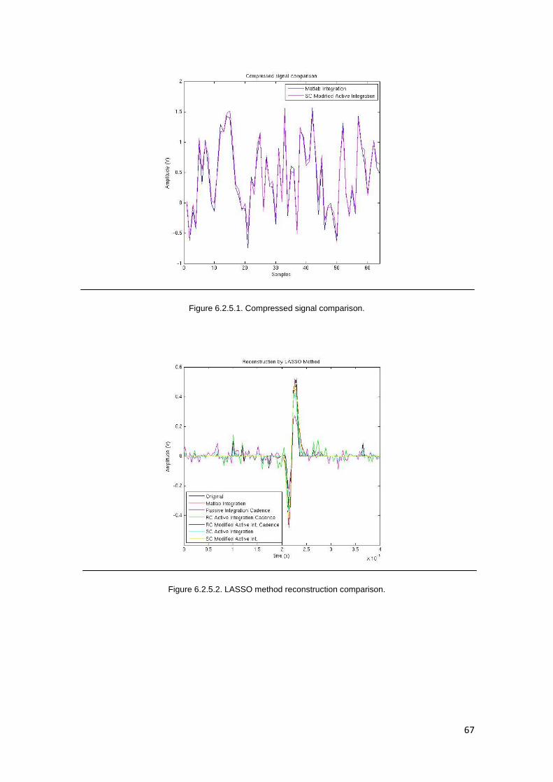
67
Figure 6.2.5.1. Compressed signal comparison.
Figure 6.2.5.2. LASSO method reconstruction comparison.

68
Figure 6.2.5.3. BPDN method reconstruction comparison.
In Fig.6.2.5.2 and Fig.6.2.5.3 input reconstruction is shown for all the ideal cases have been
tested. It is clearly observable that the best recovery for the full energy range has been
achieved by the non-inverting SC Integrator without parasitic effects (in yellow), closely followed
by the SC Integrator with parasitic effects. The continuous time configurations, in passive or
active topologies have demonstrated to carry out a worst charge and discharge of the capacitor
during the integration phases, and so the final accumulated values for each of the compressed
samples in each of the paths of the channels move away from the theoretical solution calculated
in Matlab, whereupon the reconstructed signal is more noisy than in discrete time-based
integrators. This discussion is summarized in 6.2.6 with the SNR analysis.
6.2.6. SNR Calculations [32]
Signal to Noise Ratio has been calculated by considering Eq. 23:
(23)
Where is the original input signal and is the reconstructed one. In Table 6.2.6.1 SNR
calculations for each of the ideal topologies which have been presented in 6.5 are summarized
for both of the recovery methods have been considered, LASSO-based and BPDN-based one.
According to the results obtained below, the best topology to be improved is the one presented
in 6.2.5, based on switched capacitors and enhanced not to be sensitive to the parasitic which
are introduced by C1. Henceforward, a mixing-integration real topology based on switched
capacitors is considered.

69
Topology LASSO (dB) BPDN (dB)
Matlab Code 36.3 36.9
Passive Integrator (6.5.1) 9.8 10.4
Active Integrator (6.5.2) 7.8 5.6
Modified Active Int. (6.5.3) 8.2 3.6
SC Int. Parasitic Sensitive (6.5.4) 12.7 14.7
SC Int. Parasitic Insensitive
(6.5.5)
14.1 14.9
Table 6.2.6.1. SNR comparison between topologies and reconstruction methods.
The primary advantages of SC circuits include: a) compatibility with CMOS technology; b) good
accuracy of time constants; c) good voltage linearity; d) good temperature characteristics; and
e) less area needs. By the other hand, the main disadvantages are a) clock feedthrough; b) the
requirement of nonoverlapping clock; and c) the necessity of the bandwidth of the signal being
less than the clock frequency. Beneath, these considerations are taken into account.

70
71
7. Conclusions
7.1. Remarks
As it is shown along the previous chapters, this project has been arranged as collaboration
between LSM-EPFL and IMEC. During the three months in LSM, it has been carried out a deep
study about Compressive Sensing oriented to the implementation of a system on-chip to
compress neural signals and send it by saving power consumption and heat dissipation in the
transmitter.
Due to the fact that Compressive Sensing technique applied to real implementations is in an
early phase, an extensive state of the art has been accomplished in order to be able to specify
the known limitations of the designs based on Compressive Sensing. This study encompasses
all the actual trends of design, both in digital and analog domain, and so it is considered a good
starting point for future related projects. It has been scheduled the circuit implementation of an
analog-liked multi-path/multi-channel compression system, in order to deepen into the feasibility
of this configuration instead of the digital implementation, which is the most used one even
when the available power consumption comparison between digital and analog approaches
have revealed not to be enough conclusive to dismiss the latter one.
For this purpose, foremost, a complete multichannel implementation has been developed both
in Matlab and Simulink. In order to carry through this task, a neural signal, (AP) has been
considered as sparse input. The reconstruction has been accomplished by applying BPDN and
LASSO reconstruction methods, for which the mathematical bases of Compressive Sensing
have been studied.
In order to implement a parallel and more compact random generator block to implement the
measurements matrix, a new design has been settled up in Cadence 5, by using the technology
UMC 0.18μm, for a variable number of multiple outputs.
Under the scope of the regular operation of Compressive Sensing, a new approach to this
method has been developed by realizing that sparsity conditions are fulfilled in an array of
multielectrodes. That it, if all the sensors are simultaneously sampled, according to the usual
spikes propagation among neurons, just few of these electrodes receive a peak, what results in
a spatial sparse signal which can be compressed by Compressive Sensing. This approach has
been implemented in Matlab and Cadence, and results have been submitted in the paper [31].
During the period in IMEC, in order to implement the mixer and the integrator blocks which are
need in each of the paths (rows) of a channel, a combined design has been implemented in
Cadence 6, by using the technology TSMC018.
In order to achieve a feasible analog implementation, different integrators have been tested.
Integrators in continues time domain have been proved not to be an optimal solution due to the

72
fact that in order to integrated the neural input signals in a range of frequencies till 10 kHz, the
area needed to implement the resistor and the capacitors is too large to be a design which
could spread out all over all the paths are needed in all the channels of the chip array. Due to
this, switched capacitor architecture has been deployed. By considering an implementation that
makes depend the magnitude of the components on a clock frequency, area constraints are
relaxed, so that has revealed as a practicable design to implement an analog design of the CS-
liked acquisition system.
7.2. Next steps
During the accomplishment of this project, Compressive Sensing-based systems has revealed
as a promising compression method to be applied in biological signals which satisfy sparsity
conditions.
As it is shown along the previous chapters, Compressive Sensing systems are becoming more
and more relevant in order to efficiently implement high information rate acquisition circuits.
However, it is a new methodology, and many design parameters have not been settled yet, so
the project has turned into the first approximation to an entire CS-platform based on analog
implementation for EPFL and IMEC.
After the work which is circumscribed to the scope of the master thesis, a real SC-based mixing
and integration path will be implemented in IMEC based on real components. In the same way,
LNA and ADC will be integrated along with the mixer, integrator and random generator which
have been individually designed in order to attain a complete analog path for future
multichannel implementations.
For the other hand, in order to be able to apply this array-based neural acquisition system to
record as many different neural signals as possible, it is recommended to study the best
sparsifying basis for each of the characteristic neural signals. Therefore, neural sciences could
benefit of clearer recordings in order to better understand the illness which are related with the
brain. Similarly, other reconstruction methods, as [37], could be applied and compare with the
ones have been used in this work, in order to verify which one gives the best results.
Finally, the new CS-application which has been presented [31] has to be deeper studied in
order to specify its better applicability in neural recording.

73
Appendix
Appendix A
Convex
Optimization
Basis Pursuit (BP)
Basis Pursuit De-Noising (BPDN)
Conjugate Gradients Pursuit (CGP)
Preconditioned Conjugate Gradient Pursuit (PCGP)
Iterative Greedy
Algorithms
Matching Pursuit (MP)
Orthogonal Matching Pursuit (OMP)
Regularised Orthogonal Matching Pursuit (ROMP)
Compressive Sampling Matching Pursuit (CoSaMP)
Iterative Hard Thresholding (IHT)
Iterative Shrinkage/Thresholding (IST)
Stagewise Orthogonal Matching Pursuit (StOMP)
Stagewise Weak Orthogonal Matching Pursuit (SWOMP)
Stagewise Conjugate Gradient Pursuit (StCGP)
Weak Conjugate Gradient Pursuit (SWCGP)
Stagewise and Reduced Conjugate Gradient (RCG)
Subspace Pursuit (SP)
Others
Iterative Reweighted l1-norm Minimization Algorithm
(IRWL1) + Hidden Markov Tree (HMT) model
Gradient Projection (GP)
Gradient Projection for Sparse Reconstruction (GPSR)
Least-Angle Regression (LARS)
Least Squares Quadratic Regression (LSQR)
Least Absolute Shrinkage and Selection Operator
(LASSO)
Bound Constrained Quadratic Programming (BCQP)
Interior Point (IP)
Table A.1. Main Reconstruction Methods.

74

75
Appendix B
B.1. Digital Implementation
An implementation of a hardware-efficient CS architecture in wireless sensors has been
recently proposed by Chen and Chandrakasan [3]. The CS channel that has been implemented
is shown below. As it can be observed, the main issue in this design is that the compression
operation takes place in the digital domain. The signal is acquired, amplified and forwarded to
the analog-to-digital converter (ADC), after thus, each of the M rows of the random matrix is
row-wise multiplied by the input bits in M different paths, being at the end of each path one
compressed coefficient.
Figure B.1.1 Block diagram for a digital implementation of one CS channel.
In order to implement the multiplication, a digital mixing and accumulation is carried out along
the N samples of length of the registered signal. All the operation takes place at Nyquist rate but
the final accumulation of the M compressed values of the signal. The cost of this design has
been calculated by taking into consideration the following specifications, (see Table B.1.1):
Parameter Specification
Technology 90 nm CMOS
Measurements (M) 50
Samples (N) 500
ADC bits (Bf) 8
CS signal bits (By) 10
Bandwidth (BWf) 200 Hz
Total gain (GA) >100
Table B.1.1. CS model specifications.

76
The total power cost for the digital implementation of a multipath CS encoder, without taking into
consideration the random generation, has been calculated in [3] as:
(24)
The digital CS channel, including matrix generation and clock consumption, consumes 1.9 μW
at 0.6 V for sampling frequencies below 20kS/s. In Fig. B.1.2 is included the power consumption
analysis regarding to the bandwidth of the input signal as it has been presented in [3]. By
considering the power consumption estimation of Eq.24, it is clear that the largest contribution
to the power spending is the result of the ADC and the amplifier.
Figure B.1.2. Power consumption versus bandwidth for the digital implementation of a CS path.
Specifications from Table 3.1.1 have been taken into consideration.
B.2. Analog Implementation
B.2.1. Current Mode
In [27], it is presented a current-mode circuit implementation of CS architecture to be used in a
multichannel receiver system which is used to digitize at 1.5 GHz the signals of each channel,
which are sparse in frequency domain, and spread it over the entire bandwidth. In Fig. B.2.1.1 it
is observed the circuit proposal to this application. In the approach of [27], an Operational
Transconductance Amplifier (OTA) and an ADC are considered for each of the paths. It is worth
mentioning, that the integrators consist of two time-interleaved branches which provide

77
successive integration windows in order to develop a Parallel Segmented CS (PSCS)
architecture, which achieves a decreasing in the necessary number of implemented paths per
channel.
Figure B.2.1.1. Circuit implementation of the proposed CS receiver.
By exploiting signal sparsity, the system accomplishes 44 dB overall SNRD, with a power
consumption of 120.8 mW. Others critical specifications about the design have been included in
Table B.2.1.1.
Parameter Specification
Technology 90 nm CMOS
Parallel paths 8
Chip area (8 paths) 1000 μm x 1400 μm
Bandwidth (BWf) 10 MHz - 1.5 GHz
Table B.2.1.1. CS model specifications.
B.2.2. Voltage Mode
In [3], Chen and Chandrakasan have proposed a voltage mode-based architecture for an
analog channel for a wireless neural CS implementation which has been depicted in Fig.B.2.2.1.
The registered signal is amplified by an operational transconductance ampliflier (OTA) in each
of the M paths of the CS operation, and afterwards, the N samples are multiplied by N
coefficients of the random matrix and accumulated in each of the rows before being sent at
compressed rate to the dedicated ADC which has been included in each of the paths. At the
output of each of the ADC the final digitized compressed value is acquired. The exploit of one
amplifier per channel widely increase the power consumption as it is shown in the Eq.24. In the
Chapter 3.3 the necessity of one OTA and ADC per path are deeply discussed in order to clarify
the feasibility of an analog implementation for a neural channel.
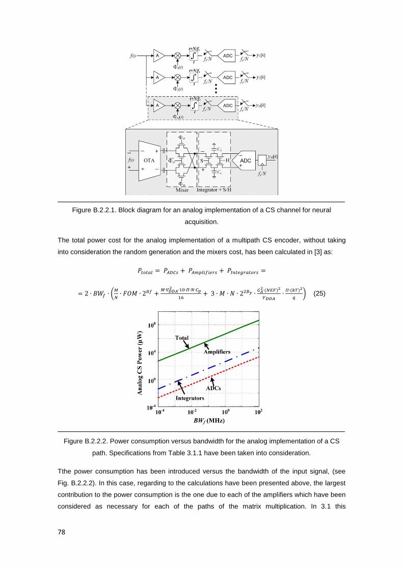
78
Figure B.2.2.1. Block diagram for an analog implementation of a CS channel for neural
acquisition.
The total power cost for the analog implementation of a multipath CS encoder, without taking
into consideration the random generation and the mixers cost, has been calculated in [3] as:
(25)
Figure B.2.2.2. Power consumption versus bandwidth for the analog implementation of a CS
path. Specifications from Table 3.1.1 have been taken into consideration.
Tthe power consumption has been introduced versus the bandwidth of the input signal, (see
Fig. B.2.2.2). In this case, regarding to the calculations have been presented above, the largest
contribution to the power consumption is the one due to each of the amplifiers which have been
considered as necessary for each of the paths of the matrix multiplication. In 3.1 this

79
approximation is discussed by taking into consideration a different block diagram, which has
been considered as a better approximation to the analog implementation of a CS path in terms
of power saving. In the same way, Chapter 6 a new path design has been considered by
exploiting an area saving on chip.
B.2.3. Charge Mode
An incremental Sigma-Delta ADC (ΣΔ-ADC), for CS applications has been submitted in [28]. The
novelty of this implementation is the simultaneity of the acquisition and quantization of CS
measurements, due to the fact that a Switched Capacitor (SC) integrator of has been
incorporated in the close loop of the converter. The converter occupies a small area of 0.047
mm2 on a target 0.5 μm CMOS process, and it can be suitable for CS applications. A sketch of
the complete implementation has been depicted in Fig. B.2.3.1.
Figure B.2.3.1. Switched Capacitor circuit implementation of the CS ADC.
In [1] it has been proposed a binary-weighted SC Multiplying Digital-to-Analog Converter
(MDAC) for the processing of ECG and EMG signals. The architecture that is included in
Fig.B.2.3.2. implements a multiplication between the actual random coefficient and the input
signal sample during Φ1 and the accumulation of this value during Φ2, these two are settled in
non-overlapping. For instead, the first random coefficient which corresponds to element row one
and column one from the random matrix, Φ11, and the first signal sample X1, are multiplied when
Φ1 is closed. When Φ2 is closed, the result is accumulated in the integration capacitance. Once
again, when Φ1 is closed, Φ12 and X2 are multiplied, and during the next high level Φ2, the result
of this operation is added to the previous value has been accumulated, and so on. The Most
Significant Bit (MSB) is used as sign bit.

80
Figure B.2.3.2. Binary-weighted SC MDAC/summer for CS.

81
Appendix C
C.1. Analog Implementation
There is a large range of applications in which random generation is necessary in order to be
used in signal processing blocks. Radiofrequency communications signal mixing, test systems
and more recently biosignal compression based on CS are the most relevant ones. By means of
an analog implementation of such randomness, a true random generation is achieved at the
expense of a larger circuit complexity of the integration of more exotic circuitry. The main
techniques have been developed are: direct amplification of noise, high-frequency oscillator
sampling and randomness generation based on chaotic systems, and they are described below.
C.1.1. Direct Amplification of Noise
This method uses a device noise to make a decision of a bit 1 or 0 depending if the signal is
greater than certain threshold or vice versa. This can be done by amplifying the white noise of a
resistor and then using a comparator to obtain a random bit. These schemes need a high-gain-
bandwidth low-offset amplifier due to the fact that if a low-bandwidth amplifier is used, the
output noise spectrum can be concentrated around DC and so, noise samples are correlated.
Thus, they are not suitable for Radio Frequency Identification, RFID, systems. An
implementation has been presented in [29], and the main architecture is shown in Fig.C.1.1.1.
This approach is not feasible to an on-chip application, due to area constraints.
Figure C.1.1.1. Random generator based on direct amplification of noise [29].
C.1.2. High-Frequency Oscillator Sampling [29]
A TRNG can be implemented by combining a low-frequency jitter clock and using it to sample a
high-frequency oscillator. The timing jitter is a stochastic phenomenon caused y thermal noise
present in the transistors of a ring oscillator. The drawback of this procedure is that the
megahertz generation is power hungry, so it is not an option for an on-chip CS design.

82
The main model is shown in Fig.C.1.2.1, it can be observed as the final random bit stream is the
result of the subsampling of a high-frequency source of oscillations and storing the
corresponding values in a D Flip-Flop, (DFF).
Figure C.1.2.1. Basic oscillator-based TRNG.

83
Appendix D
Output 4FF-PRBS Output 5FF-PFBS Output
1 3 3
2 1 2
3 1 3
4 1 4
5 1 5
6 4 2
7 4 3
8 4 4
9 4 5
10 1 1
11 2 1
12 3 1
13 4 1
14 2 5
15 2 3
16 3 5
Table D.1. Selected crosses for 16 outputs through a 4FF-PRBS and a 5FF-PRBS.

84
Appendix E
E.1. Amplification
The small amplitude of neural signals and the high impedance of the electrode-tissue interface
force to use a front-end amplifier before processing of digitizing the input signal [33]. The main
features are required in the LNA to be used are shorted in Table E.1.1.
Feature Neural Signal Amplification
Input referred noise Low to revolve spikes of 30 μV
Dynamic range ± 1-10 mV to convey EEG peaks
Input impedance Higher than the electrode-tissue interface
DC input current Negligible
Frequency band Depending on signals of interest (see Table 2.1.1)
Power Consumption Low to avoid neural tissue heating
Common Mode Rejection
Ratio (CMRR)
High in order to minimize interference from power line
noise and close proximity between electrode and
amplifier to minimize capacitive and inductive coupled
interferometers
Power Supply Rejection
Ratio (PSRR)
Table E.1.1. Main features of a front-end amplifier for neural recording.
Besides the characteristics listed behind, the LNA has to block DC offset present at the
electrode-tissue interface to prevent saturation of the amplifier and it has to consume little
silicon area and use few or no off-chip components to minimize the dimensions. An example of
OTA-based neural amplifier was presented in 2003 by Harrison and Charles.
E.2. Signal Digital Conversion
In order to achieve a robust transmission of the signals which have been registered, the
amplified and eventually compressed information has to be digitized. There is an extensive
variety of techniques for performing analog-to-digital conversion which are included in Fig.E.2.1.
Choice of one specific technique depends on the signal of interest, as well as the area and
power constraints which have to be faced by the designer. As it is depicted below, a data rate of
15 kS/s is enough in most of clinical applications, but it requires a data stream of 15Mb/s for 100
electrodes, which is impossible to transmit across the skull and the scalp. RF links are limited by
the tissue electromagnetic absorption, which follows an f2 ratio.

85
Figure E.2.1. Several techniques to digitize different kind of neural signals.

86

87
Glossary
ADC: Analog-to-Digital Converter
AP: Action potential
BAN: Body Area Network
BCI: Brain-Computer Interface
BCQP: Bound Constrained Quadratic Programming
BP: Basis Pursuit
BPDN : Basis Pursuit De-Noising
BW : Bandwithd
CGP : Conjugate Gradients Pursuit
CS : Compressive Sensing or Compressive Sampling
CoSaMP: Compressive Sampling Matching Pursuit
ECG: Electrocardiogram
ECoG: Electrocorticogram
EEG: Eectroencefalogram
GP: Gradient Projection
GPSR: Gradient Projection for Sparse Reconstruction (GPSR)
HMT: Hidden Markov Tree
IHT: Iterative Hard Thresholding
IP: Interior Point
IRWL1: Iterative Reweighted l1-norm Minimization Algorithm
IST: Iterative Shrinkage/Thresholding
LARS: Least-Angle Regression
LASSO: Least Absolute Shrinkage and Selection Operator
LFSR: Linear Feedback Shift Register
LNA: Low Noise Amplifier
LPF: Low Pass Filter

88
LSQR: Least Squares Quadratic Regression
MDAC: Multiplying Digital-to-Analog Converter
MP: Matching Pursuit MP
MSB: More Significant Bit
OMP: Orthogonal Matching Pursuit
OTA: Operational Transconductance Amplifier
PCGP: Preconditioned Conjugate Gradient Pursuit
PRBS : Pseudorandom Binary Sequence
PSD: Power Spectra Density
RAmP: Restricted Amplification Property
RC: Random Convolution
RFID: Radio Frequency Identification
RIP: Restricted
RDG: Reduced Conjugate Gradient
ROMP: Regularised Orthogonal Matching Pursuit
SC: Switched Capacitor
SCS: Spatial Compressive Sensing
SNR: Signal-to-Noise Ratio
StCGP: Stagewise Conjugate Gradient Pursuit
StOMP: Stagewise Orthogonal Matching Pursuit
SP: Subspace Pursuit
SWOMP: Stagewise Weak Orthogonal Matching Pursuit
TRNG: True Random Number Generation
WCGP: Weak Conjugate Gradient Pursuit

89
References
[1] D. Gangopadhyay et al. System Considerations for the Compressive Sampling of EEG and ECoG Bio-
signals. IEEE, pp.129-132, 2011.
[2] R.F: Yazicioglu et al. Ultra-low-Power Wearable Biopotential Sensor Nodes. 31th
Annual International
Conference of the IEEE, pp. 3205-3208, 2009.
[3] F. Chen et al. Design and Analysis of a Hardware-Efficient Compressed Sensing Architecture for Data
Compression in Wireless Sensors. IEEE Journal of Solid-State Circuits, vol.47, no.3, pp .744-756, 2012.
[4] W. Wattanapanitch et al. An energy-efficient micropower neural recording amplifier, IEEE Trans.
Biomed. Circuits Syst., vol. 1, no. 2, pp. 136–147, 2007.
[5] B. Murmann, A/D converter trends: Power dissipation, scaling and digitally assisted architectures, Proc.
2008 IEEE Custom Integrated Circuits Conf., vol. 1, pp. 105–112, 2008.
[6] N. Verma et al. A micro-power EEG acquisition SoC with integrated feature extraction processor for a
chronic seizure detection system, IEEE J. Solid-State Circuits, vol. 45, no. 4, pp. 804–816, 2010.
[7] V. Karkare, et al., A 130- W, 64-channel spike-sorting DSP chip, Proc. IEEE Asian Solid-State Circuits
Conf., vol. 1, pp. 289–292, 2009.
[8] J. L. Bohorquez et al., A 350 W CMOS MSK transmitter and 400 W OOK super-regenerative receiver
for medical implant communications, Symp. VLSI Circuits Dig. Tech. Papers, pp. 32–33, 2008.
[9] C.T. Nordhausen et al., Single unit recording capabilities of a 100 microelectrode array, Brain Res., vol.
726, pp. 129-140, 1996.
[10] B. Gosselin, Recent Advanced in Neural Recording Microsystems, Sensors(11), pp. 4572-4597, 2011.
[11] V. B. MountCastle, Modality and topography properties of single neurons of cat’s somatic sensory
cortex, J. Neurophysiol. no.20, pp. 408-434, 1957.
[12] D. H. Hubel et al., Receptive Fields of Single Neurones in the cat’s striade cortex, J. Physiol., no.148,
pp. 574-591, 1959.
[13] A. P. Georgopoulos et al., Neural population coding of movement direction, Science, no.233, pp.
1416-1419, 1986.
[14] A. B. Schwartz et al., Primate motor cortex and free arm movments to visual targets in three-
dimensional space, J. Neurophysiol., no.8, pp. 2913-2927, 1988.
[15] D. M. Taylor et al., Direct Cortical Control of 3D neuroprosthetic devices, Sciences, no 296, pp.1829-
1832, 2002.
[16] J. Wessberg et al., Real-time prediction of hand trajectory by ensembles of cortical neurons in
primates, Nature, no. 408, pp. 361-365, 2000.

90
[17] L. R. Hochberg et al., Neuronal ensemble control of prosthetic devices by a human with tetrapejia,
Nature, no. 442, pp. 164-171, 2006.
[18] M. Fornsier et al., Compressive Sensing, pp. 1-49, 2010.
[19] P. T. Boufounos et al., 1-Bit Compressive Sensing, IEEE 42nd Annual Conference on Information
Sciences and Systems, pp. 16-21 , 2008.
[20] M. F. Duarte et al., Kronecker Compressive Sensing, IEEE IEEE Transactions on Image Processing,
vol. 21, pp.494-504, 2012.
[21] V. Majidzadeh et al., A (256x256) Pixel 76.7 mW CMOS Imager/Compressor Based on Real-Time In-
Pixel Compressive Sensing, IEEE Proceedings of the IEEE International Symposium on Circuits and
Systems (ISCAS), pp.2956-2859, 2010.
[22] R. G. Baraniuk et al., Model-Based Compressive Sensing, IEEE Transactions Theory, vol.56, no.4,
pp. 1982-2001, 2010.
[23] B. Murmann, A/D Converter trends: power dissipation, scaling and digitally assisted architectures,
Proc. IEEE Custom Integrated Circuits Conf, vol.1, pp.105-112, 2008.
[24] C. Hegde, Compressive Sensing Recovery of Spikes Trains using s Structured Sparsity Model, Proc.
Signal Process. Adaptive Sparse Structured Representations, 2009.
[25] E. J. Càndes, Compressive Sampling, Int. Congress of Mathematics, 3, pp. 1433-1452, 2006.
[26] E. J. Càndes et al., Compressed Sensing Makes every Pixel Counts, What’s happening in the
Mathematical Sciences, pp.114-127.
[27] Xi Chen et al., A Sub-Nyquist Rate Sampling Receiver Exploiting Compressive Sensing, IEEE
Transactions Circuits and Systems, pp.507-520, 2010.
[28] Hsuang-Tsung Wang et al., An incremental Sigma Delta Converter for Compressive Sensing
Appliciations, IEEE, pp.522-524, 2011.
[29] C. S. Petrie et al., Modeling and Simulation of oscillator-based Random Number Generators, IEEE,
pp. 324-327, 1996.
[30] E. V. Berg and M. P. Friedlander, “SPGL1: A solver for large-scale sparse reconstruction”, June 2007.
[Online]. Available: http://www.cs.ubc.ca/labs/scl/spgl1
[31] M. Shoaran, M. Maqueda et al., Circuit-Level Implementation of Compressed Sensing for Multi
Channel Neural Recording, 2012 [Submitted to BIOCAS 2012].
[32] P. E. Allen, D. R. Holberg, CMOS Analog Design Circuits, 2th Edition, Oxford University Press, 2002.
[33] R. R. Harrison, The design of Integrated Circuits to Observe Brain Activity, Proc. of the IEEE, vol. 96,
pp. 1203-1216, 2008.
[34] M. F. Duarte et. al., Wavelet-Domain Compressive Signal Reconstruction using a Hidden Markov Tree
Model. IEEE International Conf. 2008, pp. 5137–5140.

91
[35] M.F. Duarte et. al., Recovery of Compressible Signals in Unions of Subspaces. Information Sciences
and Systems, pp. 175-180, 2009.
[36] H. Mamaghanian et. al., Compressed Sensing for Real-Time Energy-Efficient ECG Compression on
Wireless Body Sensor Nodes, IEEE Trans. on Biomedical Eng., vol.58, pp. 2456 - 2466, 2012.
[37] S. Boyd et al., Convex Optimization. [Online]. Available: http://www.stanford.edu/~boyd/software.html.