Embed Size (px)
Citation preview
7/27/2019 Tharaneeswaran Phase 1 Final Review
http://slidepdf.com/reader/full/tharaneeswaran-phase-1-final-review 1/16
Leakage Current Monitoring And Comparing In NMOS At
Standby Mode
Guided By Submitted By
Dr.J.Raja Paul Perinbam PhD Tharaneeswaran.T [1054819]
Professor II M.E.,[VLSI Design]RMK Engineering College RMK Engineering College
7/27/2019 Tharaneeswaran Phase 1 Final Review
http://slidepdf.com/reader/full/tharaneeswaran-phase-1-final-review 2/16
Overview
20th December,2011
2
Introduction
Objective
Literature Survey
Implemented System
Simulation Results
7/27/2019 Tharaneeswaran Phase 1 Final Review
http://slidepdf.com/reader/full/tharaneeswaran-phase-1-final-review 3/16
Introduction
20th December,2011
3
Scaling down the Size of Transistors Improve thespeed of devices, density of chip, lower powerdissipation.
To decrease power consumption supply voltage haveto be scaled, which in turn increase sub-thresholdleakage current severely affecting power dissipation.
In MOS transistors, current is consumed even inOff-state or Standby Mode.
7/27/2019 Tharaneeswaran Phase 1 Final Review
http://slidepdf.com/reader/full/tharaneeswaran-phase-1-final-review 4/16
Objective
20th December,2011
4
Leakage current is monitored by Setting theSubstrate Bias Voltage to Control the Transistor
Threshold Voltage.
Total minimum leakage is found by comparing sub-
threshold current (ISUB) and band-to-band current
(IBTBT).

7/27/2019 Tharaneeswaran Phase 1 Final Review
http://slidepdf.com/reader/full/tharaneeswaran-phase-1-final-review 5/16
Literature Survey
20th December,2011
5
Kaushik Roy, et al (2003) reviews various transistor intrinsic leakage
mechanisms. High leakage current in deep-sub micrometer regimes is a
significant contributor to power dissipation in CMOS circuits as threshold
voltage, channel length, and gate oxide thickness are reduced. The
identification of different leakage components is very important for estimation
and reduction of leakage power, especially for low-power applications.
Cassondra Neau, Kaushik Roy et al (2003) presented a techniques to
determine the optimal body bias to minimize leakage current and compensate
process variations in scaled CMOS technologies. A circuit trades off sub-threshold leakage with band-to-band tunneling leakage at the source/drain
junctions to determine the optimal substrate bias for different technology
generations and under process variations.
7/27/2019 Tharaneeswaran Phase 1 Final Review
http://slidepdf.com/reader/full/tharaneeswaran-phase-1-final-review 6/16
Literature Survey (cont..)
20th December,2011
6
Kyung Ki Kim, Yong-Bin Kim, Minsu Choi, Nohpill Park et al (2007)
estimated the total leakage power is critical to designing low-power digital
circuits. To improve performance, it is necessary to reduce the threshold
voltage (Vth) as well, which results in an exponential increase of sub threshold
leakage.
H. Jeon, Y.-B. Kim, and M. Choi et al (2009) proposed a novel approach to
minimize leakage current in CMOS circuit during the off-state (or standby
mode, sleep mode) by setting the optimal substrate bias voltage to control the
transistor threshold voltage. The total minimum leakage current is found by
comparing the sub threshold current and band-to-band current .

7/27/2019 Tharaneeswaran Phase 1 Final Review
http://slidepdf.com/reader/full/tharaneeswaran-phase-1-final-review 7/16
Implemented System
20th December,2011
7
7/27/2019 Tharaneeswaran Phase 1 Final Review
http://slidepdf.com/reader/full/tharaneeswaran-phase-1-final-review 8/16
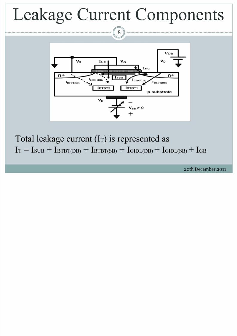
Leakage Current Components
20th December,2011
8
Total leakage current (IT) is represented as
IT = ISUB + IBTBT(DB) + IBTBT(SB) + IGIDL(DB) + IGIDL(SB) + IGB

7/27/2019 Tharaneeswaran Phase 1 Final Review
http://slidepdf.com/reader/full/tharaneeswaran-phase-1-final-review 9/16
Monitoring Circuit
20th December,2011
9
7/27/2019 Tharaneeswaran Phase 1 Final Review
http://slidepdf.com/reader/full/tharaneeswaran-phase-1-final-review 10/16
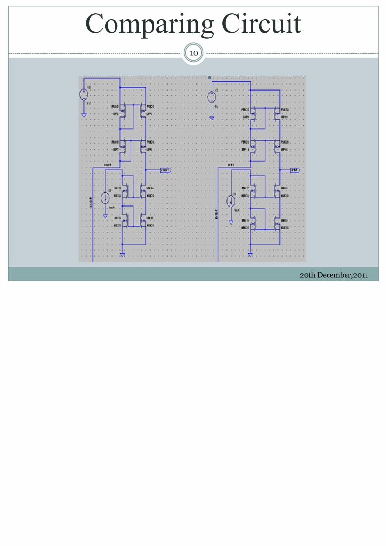
Comparing Circuit
20th December,2011
10
7/27/2019 Tharaneeswaran Phase 1 Final Review
http://slidepdf.com/reader/full/tharaneeswaran-phase-1-final-review 11/16
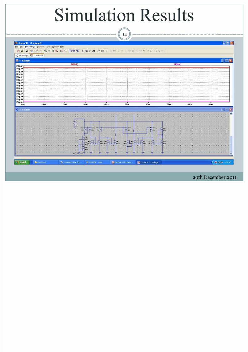
Simulation Results
20th December,2011
11
7/27/2019 Tharaneeswaran Phase 1 Final Review
http://slidepdf.com/reader/full/tharaneeswaran-phase-1-final-review 12/16
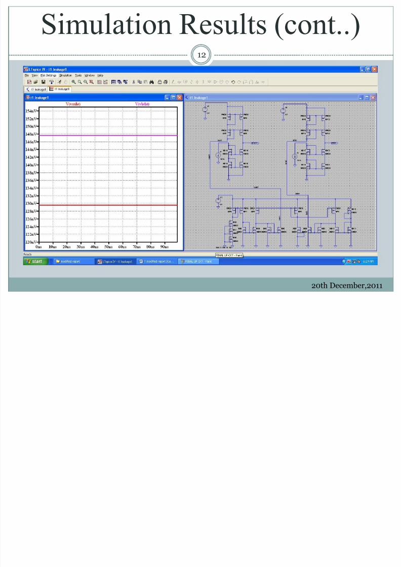
Simulation Results (cont..)
20th December,2011
12

7/27/2019 Tharaneeswaran Phase 1 Final Review
http://slidepdf.com/reader/full/tharaneeswaran-phase-1-final-review 13/16
Conclusion
20th December,2011
13
Project work phase I presents a system for leakage
current monitoring and comparing in CMOS Integrated
circuits through which the leakage currents are detectedand simulated.
The simulated currents are then given to the current
comparator circuit which in turn produces the output
voltage in the pulse width manner.
7/27/2019 Tharaneeswaran Phase 1 Final Review
http://slidepdf.com/reader/full/tharaneeswaran-phase-1-final-review 14/16
Future Work
20th December,2011
14
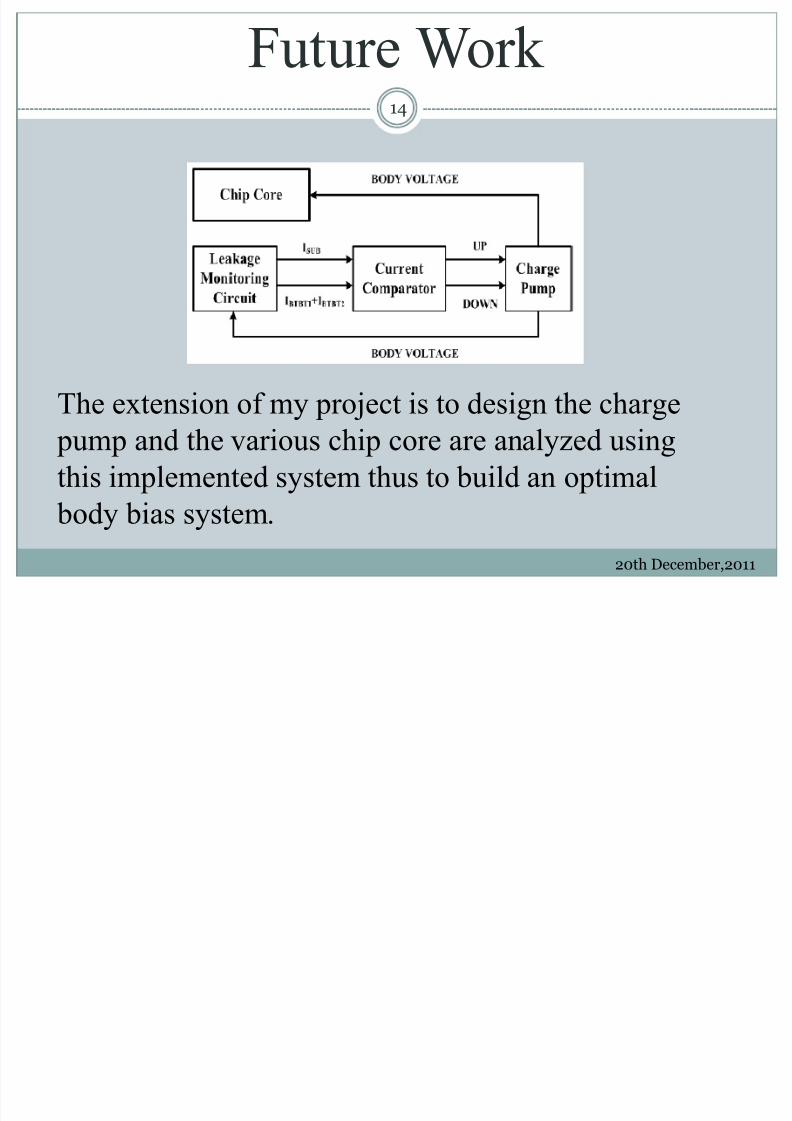
The extension of my project is to design the charge pump and the various chip core are analyzed using
this implemented system thus to build an optimal
body bias system.
7/27/2019 Tharaneeswaran Phase 1 Final Review
http://slidepdf.com/reader/full/tharaneeswaran-phase-1-final-review 15/16
References
20th December,2011
15
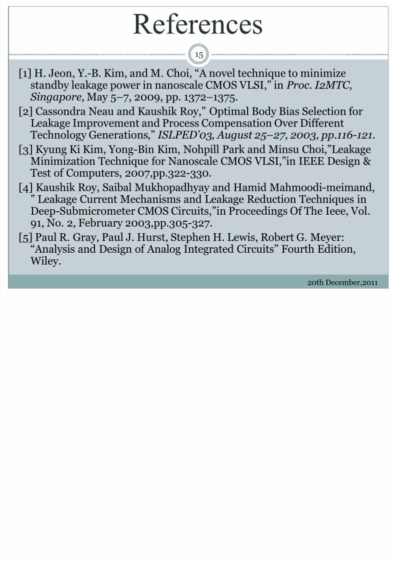
[1] H. Jeon, Y.-B. Kim, and M. Choi, “A novel technique to minimizestandby leakage power in nanoscale CMOS VLSI,” in Proc. I2MTC, Singapore, May 5–7, 2009, pp. 1372–1375.
[2] Cassondra Neau and Kaushik Roy,” Optimal Body Bias Selection forLeakage Improvement and Process Compensation Over Different
Technology Generations,” ISLPED’03, August 25–27, 2003, pp.116-121.[3] Kyung Ki Kim, Yong-Bin Kim, Nohpill Park and Minsu Choi,”Leakage
Minimization Technique for Nanoscale CMOS VLSI,”in IEEE Design &Test of Computers, 2007,pp.322-330.
[4] Kaushik Roy, Saibal Mukhopadhyay and Hamid Mahmoodi-meimand,” Leakage Current Mechanisms and Leakage Reduction Techniques in
Deep-Submicrometer CMOS Circuits,”in Proceedings Of The Ieee, Vol.91, No. 2, February 2003,pp.305-327.
[5] Paul R. Gray, Paul J. Hurst, Stephen H. Lewis, Robert G. Meyer:“Analysis and Design of Analog Integrated Circuits” Fourth Edition, Wiley.

7/27/2019 Tharaneeswaran Phase 1 Final Review
http://slidepdf.com/reader/full/tharaneeswaran-phase-1-final-review 16/16
20th December,2011
16


![[Draft]/[Final] Review Report î ì í8 Second phase of](https://img.pdfslide.net/doc/110x75/62790999fb14b95d557c5639/draftfinal-review-report-8-second-phase-of-.jpg)