Embed Size (px)
Citation preview
The Air Stability and Operational Lifetime of
Organic Photovoltaic Materials and Devices
Edward S. R. Bovill
Department of Physics and Astronomy
University of Sheffield
Thesis submitted for the degree of
Doctor of Philosophy
February 2015


Acknowledgements Page I
Acknowledgements
I would like to take this opportunity to thank everyone who has made this work possible, both
through their academic and moral support. Firstly, I would like to thank my supervisor David
Lidzey for providing me with the support needed throughout the last few years. You have
been a font of knowledge, and I could not have achieved this without your steady guiding
hand. I would also like to thank all the members of the EPMM group and Ossila Ltd, both
past and present, for all of their help and training. It has been a pleasure working with you all.
Without the unconditional love and support I have received from my amazing family this
work would not have been possible. Throughout my academic career, my parents have been
truly fantastic, always taking a keen interest in my work and willing to lend a hand whenever
one was needed (wielding a carrot or stick, or presenting a shoulder to cry on as required).
They have been there for me during the best and the worst of times, and I couldn't have
wished for a more loving and nurturing environment. A big thank you to my brother Will,
who always brings a big smile to my face, and drags me outside to do something active and
fun whenever we get together. Long may it continue!
My friends have provided endless laughter and great memories for many years, and so thank
you to Will, S-J, Ditts, Swatts, Trewin, Stuart, Milan, Elisa, Claire and Sarah.
Finally, I would like to thank my girlfriend Sharmin for being the wonderful person she is.
The final years of my Ph.D. have been brightened by her presence, and her unconditional
love, support and laughter have provided me with the strength to be the best I can.
Abstract Page II
Abstract
Replacing energy intensive evaporated materials with solution processed alternatives is key to
allowing OPVs to be fabricated using processes such as roll-to-roll (R2R) fabrication.
However, roll-to-roll fabrication is primarily an ambient processing method, and as such the
materials used need to be stable in the presence of oxygen and moisture. The effects of
ambient oxygen and moisture on materials utilised in OPV devices are well documented, and
in almost all cases are detrimental to device performance. Therefore, identifying materials and
techniques that address these difficulties are essential.
In this thesis, using a combination of spectroscopic techniques and device characterisation, it
is shown that applying optimised thermal treatments can reduce the uptake of moisture in
molybdenum oxide hole transport layers, and reduce the resulting negative effects on device
performance. The air stability, and therefore suitability for R2R fabrication, of several
polymers are investigated. PFDT2BT-8 was identified as the most stable, and was utilised to
fabricate OPV devices from solution in air using a variety of materials with efficiencies > 5%.
In addition, the development of lifetime testing techniques, both in a laboratory and outdoor
setting, evidencing operating lifetimes of > 7 years for devices utilising ambient solution
processed materials.
In conclusion, this thesis describes the development of materials and techniques to allow for
the fabrication of organic photovoltaic (OPV) devices from solution under ambient
conditions, having high efficiencies and long operating lifetimes.
Publications Page III
Publications
1. Edward S. R. Bovill, Jonathan Griffin, Tao Wang, James Kingsley, Hunan Yi, Ahmed
Iraqi, Alastair R. Buckley, David G. Lidzey. Air processed organic photovoltaic devices
incorporating a MoOx anode buffer layer, Applied Physics Letters, 2013, 102, 183303
2. Edward S. R. Bovill, Hunan Yi, Ahmed Iraqi, David G. Lidzey, The fabrication of
polyfluorene and polycarbazole-based photovoltaic devices using an air-stable process route,
Applied Physics Letters, 2014, 105, 223302
3. Edward S. R. Bovill, Nick Scarratt, Jonathan Griffin, Hunan Yi, Ahmed Iraqi, Alastair R.
Buckley, James W. Kingsley, David G. Lidzey, The role of the hole-extraction layer in
determining the operational stability of a polycarbazole:fullerene bulk-heterojunction
photovoltaic device, Applied Physics Letters, 2015, 106, 073301
4. Keith T. Butler, Edward S. R. Bovill, Rachel Crespo-Ortero, David O. Scanlon, David G.
Lidzey and Aron Walsh, Work function engineering of air processed hole transport layers in
organic photovoltaics: understanding and controlling oxide surface hydration effects,
Submitted for review to Chemistry of Materials June 2015 (first stage).

Conference Presentations Page IV
Conference Presentations
Oral Presentations:
European Optical Society Annual Meeting (EOSAM). Aberdeen, Scotland, UK, September
2012
UK semiconductors Summer Meeting 2013. Sheffield, UK, July 2013
Hybrid and Organic Photovoltaics 2014 (HOPV14). Lausanne, Switzerland, May 2014
Poster Presentations:
Materials Research Society (MRS) Spring Meeting. San Francisco, USA, April 2014

Table of Contents Page V
Table of Contents
Chapter 1 : Introduction .................................................................................... 1
1.1 Thesis Summary and Motivation .......................................................................................... 5
1.2 References ............................................................................................................................ 8
Chapter 2 : Background Theory ...................................................................... 11
2.0 Introduction ........................................................................................................................ 11
2.1 Atomic and Molecular Orbitals .......................................................................................... 12
2.2 Orbital Hybridization .......................................................................................................... 14
2.3 Conjugation ........................................................................................................................ 18
2.4 Photophysics of Organic Conjugated Polymers ................................................................. 19
2.4.1 Exciton Formation ....................................................................................................... 20
2.4.2 Exciton Diffusion and Dissociation ............................................................................. 22
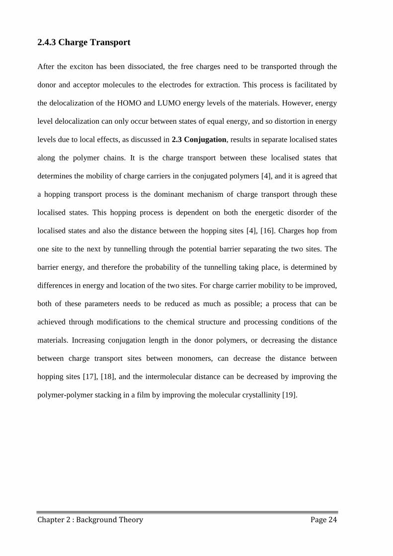
2.4.3 Charge Transport ......................................................................................................... 24
2.4.4 Charge Extraction ........................................................................................................ 25
2.5 Device Architecture ............................................................................................................ 28
2.6 Interface Materials .............................................................................................................. 32
2.6.1 PEDOT:PSS ................................................................................................................. 32
2.6.2 Transition Metal Oxides .............................................................................................. 33
2.7 Active Layer Materials ....................................................................................................... 35
2.7.1 Polymer List ................................................................................................................. 39
2.7.2 Fullerenes ..................................................................................................................... 42
2.8 Ambient Processing ............................................................................................................ 43
2.9 OPV Stability and Degradation .......................................................................................... 46
2.9.1 Photochemical Reactions ............................................................................................. 48
2.9.2 Trap Formation ............................................................................................................ 48
2.9.3 Phase Separation .......................................................................................................... 49
2.9.4 Delamination ................................................................................................................ 49
2.9.5 Encapsulation ............................................................................................................... 50
2.9.6 Decay Behaviour .......................................................................................................... 51
2.10 References ........................................................................................................................ 53

Table of Contents Page VI
Chapter 3 : Experimental Methods ................................................................. 69
3.0 Introduction ........................................................................................................................ 69
3.1 Fabrication Techniques ...................................................................................................... 70
3.1.1 Substrate Cleaning ....................................................................................................... 71
3.1.2 Solution Preparation .................................................................................................... 72
3.1.3 Thin Film Deposition .................................................................................................. 73
3.1.4 Thermal Evaporation ................................................................................................... 76
3.2 Device Fabrication ............................................................................................................. 78
3.3 Device Characterization ..................................................................................................... 81
3.3.1 Device Characterization Setup .................................................................................... 85
3.3.2 Solar Simulator Calibration ......................................................................................... 86
3.3.3 Aperture Mask Calibration .......................................................................................... 88
3.4 Absorbance Spectroscopy .................................................................................................. 89
3.5 Spectroscopic Ellipsometry ................................................................................................ 92
3.6 External Quantum Efficiency (EQE) ................................................................................. 93
3.7 Laser Beam Induced Current Mapping (LBIC) ................................................................. 94
3.8 Electroluminescence Mapping (ELM) ............................................................................... 95
3.9 Lifetime Testing ................................................................................................................. 96
3.9.1 Laboratory Lifetime Testing Setup ............................................................................. 97
3.9.2 Light Source and Spectrum ......................................................................................... 99
3.9.3 JV Mismatch .............................................................................................................. 101
3.9.4 Light Uniformity ....................................................................................................... 104
3.9.5 Source-Measure Unit Comparison ............................................................................ 105
3.9.6 Pixel Size Variation ................................................................................................... 106
3.9.7 Discrepancies in JV data............................................................................................ 108
3.10 Outdoor Lifetime Testing............................................................................................... 110
3.11 Lifetime Reporting ......................................................................................................... 113
3.11.1 ISOS Laboratory Weathering Testing ..................................................................... 113
3.11.2 ISOS Outdoor Testing ............................................................................................. 116
3.12 Conclusions .................................................................................................................... 117
3.13 References ...................................................................................................................... 119

Table of Contents Page VII
Chapter 4 : Air Stability of MoOx ................................................................. 123
4.0 Introduction ...................................................................................................................... 124
4.1 MoOx Films and Ambient Conditions .............................................................................. 125
4.2 MoOx Film and Device Preparation ................................................................................. 126
4.3 OPV Performance ............................................................................................................. 127
4.3 Water Adsorption ............................................................................................................. 133
4.4 Air Processing Photoactive Layers ................................................................................... 136
4.5 Conclusions ...................................................................................................................... 139
4.6 References ........................................................................................................................ 140
Chapter 5 : Hole Transport Layer Laboratory Lifetime Study ................. 143
5.0 Introduction ...................................................................................................................... 144
5.1 Hole Transport Layer Materials ....................................................................................... 145
5.1.1 PEDOT:PSS ............................................................................................................... 145
5.1.2 Vanadium Oxide ........................................................................................................ 146
5.2 Device Lifetime ................................................................................................................ 147
5.3 LBIC/ELM of Aged Devices ............................................................................................ 155
5.4 Conclusions ...................................................................................................................... 158
5.5 References ........................................................................................................................ 159
Chapter 6 : Polymer Air Processing .............................................................. 165
6.0 Introduction ...................................................................................................................... 166
6.1 Polymers for Air Processing ............................................................................................. 166
6.2 Fabricating OPVs in Air ................................................................................................... 170
6.3 Photostability of Polymers................................................................................................ 176
6.4 Effects of Extended Air Exposure .................................................................................... 178
6.5 Conclusions ...................................................................................................................... 182
6.6 References ........................................................................................................................ 183
Table of Contents Page VIII
Chapter 7 : Outdoor Lifetime Testing........................................................... 189
7.0 Introduction ...................................................................................................................... 190
7.1 Light and Temperature Variation ..................................................................................... 191
7.1.2 Sunny and Cloudy Days ............................................................................................ 193
7.2 Temperature Effects ......................................................................................................... 196
7.3 JV Characteristics ............................................................................................................. 198
7.4 OPV Device Lifetime ....................................................................................................... 200
7.5 Conclusions ...................................................................................................................... 203
7.6 References ........................................................................................................................ 204
Chapter 8 : Solution Processed OPVs ........................................................... 207
8.0 Introduction ...................................................................................................................... 208
8.1 Titanium Oxide ................................................................................................................ 209
8.2 Solution Processed Devices ............................................................................................. 210
8.3 Conclusions ...................................................................................................................... 215
8.4 References ........................................................................................................................ 216
Chapter 9 : Conclusions .................................................................................. 219
9.0 Conclusions of Work Undertaken .................................................................................... 219
9.1 Suggestions for Further Work .......................................................................................... 223
9.2 References ........................................................................................................................ 225
Appendix .......................................................................................................... 229
Chapter 1 : Introduction Page 1
Chapter 1 : Introduction
In 2013, the total power consumption of the world's population rose to 17.4 TW [1], an
increase of 2.3% on 2012. At the current rate of growth, by 2030 global energy production
will need to exceed 24 TW. However, as the world's population continues to grow and more
countries become industrialised, the energy needs of the world's population will, in all
likelihood, far exceed this figure. Currently, 87% of the world's energy is produced from
burning fossil fuels (including coal, gas and oil), 4% from nuclear fuels, and only 9% from
renewable sources (including hydroelectric and other technologies) [1]. There is great impetus
for change in the way energy is generated due to the increased awareness of the effects of
global warming and humanity's influence on the climate. Several meetings of the world's most
powerful leaders have produced guidelines and protocols to curb the generation of greenhouse
gasses through investment into renewable energy sources and reducing our reliance on fossil
fuels, though their success is yet to be proved. Unfortunately, excluding hydroelectricity,
other renewable energy technologies only accounted for 2.2% of global energy production, a
small increase of 0.3% from 2012. Growth in this sector has been hampered by challenges
posed by the technologies themselves and by reduced governmental investment due to global
recession. However, an optimistic report predicted that it could be possible to generate all our
energy needs using only renewable sources such as wind, wave and solar by 2050 if the social
and political barriers to implementation are overcome [2].
The Sun is a phenomenal source of energy, with the surface of Earth irradiated with ~ 100
petajoules (1015
W) of energy every second [3], roughly 6000 times the current world
consumption. This abundance of energy can be harvested through the use of photovoltaic
Chapter 1 : Introduction Page 2
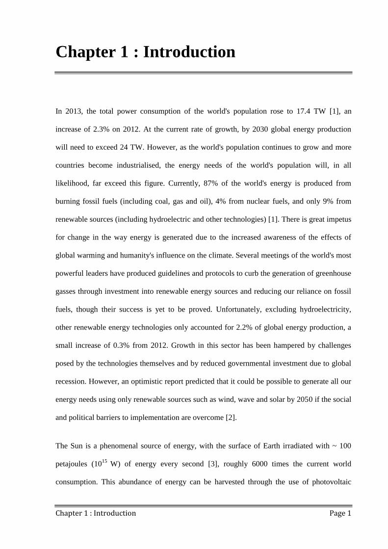
panels that convert the incident light into electricity via the photoelectric effect. The solar
spectrum incident on the Earth's atmosphere and the surface is shown in Figure 1.1, and are
known as AM0 and AM1.5 respectively. The difference in the spectra arise from adjustments
due to absorption in the atmosphere and to account for scattering. AM, which stands for air
mass, accounts for the depth of atmosphere the light passes through, with 1 being one
atmosphere depth. Many industrialised nations are located in temperate latitudes and so the
sun is not directly overhead. Therefore the AM1.5 spectrum was calculated for
standardisation purposes based on an analysis of solar irradiance data [4]. All standardised
testing of photovoltaic devices is carried out under AM1.5 spectra at 1000 Wm-2
[4].
Figure 1.1 Solar spectrum incident on the Earth above the atmosphere (AM0) and on the
surface at temperate latitudes (AM1.5). [4]
Chapter 1 : Introduction Page 3
The majority of photovoltaic (PV) panels available today are based on silicon, a technology
that has been in development for > 60 years. The efficiency of silicon PV has increased from
10% in 1955 [5] to around 25% for modern, single crystal silicon panels [6]. These high
efficiencies are due to silicon's low bandgap of 1.1 eV, allowing for efficient absorption of the
solar spectrum in the 400 - 800 nm region, and the material's excellent charge generation
properties. However, crystalline silicon, like many inorganic semiconductors, has an indirect
bandgap that necessitates thick active layers, which increases the cost of manufacture
significantly.
There are many alternative material systems for photovoltaic devices, including other
inorganic materials such as gallium arsenide (GaAs), indium phosphide (InP), cadmium
telluride (CdTe) and various other combinations of III-V elements, with maximum
efficiencies of 39.3% for a GaInP2/GaAs/Ge multijunction cell [7]. However, the market for
solar panels is dominated by silicon, with a > 90% share [8]. The other, more efficient and far
more expensive inorganic PV technologies are reserved for specialist applications including
spacecraft and satellites.
Due to the negligible running costs of solar panels during their lifetime, the only feasible way
of reducing the costs to the end user, and therefore making them more attractive to both
businesses and private users, is to reduce the cost of manufacture or increase operating
efficiency. Unfortunately, increases in device efficiency usually mean increasing the costs,
due to the necessity of using more expensive materials or more complex device architectures,
such as tandem cells and concentrators. Therefore, reducing the costs of PV requires the use
of cheap materials and manufacturing processes.
Chapter 1 : Introduction Page 4
Another type of PV technology that addresses many of the issues with inorganic PV are
organic photovoltaic devices (OPVs). These promise thin, flexible, and lightweight devices
that overcome the cost of inorganic PV by being primarily composed of carbon based
compounds. These compounds can be deposited from solution, allowing for use of cheap
manufacturing processes, such as spray coating and roll-to-roll processing, to produce large
area devices extremely rapidly. Unlike many forms of inorganic PV, which need to be
fabricated onto ultra-pure crystalline substrates, OPVs can be fabricated onto amorphous
substrate materials such as glass and flexible plastics such as PET [9], [10]. This not only
lowers the costs of manufacture, but also the embodied energy cost of the devices themselves.
However, there are several challenges inherent in OPV technology that will need to be
overcome before commercialization is possible. The optimal active layer thickness of the
device if often between 50 - 100 nm due to the semiconducting materials used having high
absorption co-efficients and poor charge mobility. This poses a challenge in device
manufacture as dust or other impurities present during device fabrication can lead to short
circuits and other defects. The charges generated on photoexcitation are strongly bound by
coulombic attraction as excitons, which leads to large binding energies and was long thought
to limit the potential maximum efficiency of OPVs to around 15% [11], though this has been
recently revised upwards to 20 - 24% [12]. Also, the stability of OPV devices is still limited
due to the oxygen and moisture sensitivity of the materials used, which requires high grade
encapsulation with very low moisture and oxygen ingress rates [13]. Large scale production
of OPVs is still in its infancy, but promising first steps have been made, albeit with devices of
< 4% efficiency [14], [15]. Finally, the ubiquitous use of indium tin oxide (ITO) as the anode
material, although also common in flat panel TVs, smart phones and other electronic devices,
is also problematic due to the scarcity of indium. The current aim of the OPV community is to
attain device efficiencies of 10% and operating lifetimes of 10 years, though economic
Chapter 1 : Introduction Page 5
assessments have shown that the technology could be competitive with silicon PV with
efficiencies of only 7% and 5 years lifetime [16]. Though these goals have not yet been met,
promising steps have been made towards both targets [17], [18].
1.1 Thesis Summary and Motivation
This work will investigate the materials and processes needed to manufacture OPVs from
solution in an ambient atmosphere, with the aim of producing fully solution processed devices
with long operating lifetimes. One of the aims of the OPV field is to develop methods and
materials that allow for the production of high efficiency and stable devices using commercial
deposition techniques, such as roll-to-roll printing and spray coating. Two of the requirements
for these processes are that the materials can be deposited from solution in air. To this end, a
variety of active layer and interlayer materials are studied, various processes developed that
allow for ambient processing with little loss in efficiency, and lifetime tests are carried out
using custom built systems. The structure of the thesis is as follows:
Chapter 2 gives an overview of the background theory of organic semiconductors and
interface materials and their use in OPVs. The experimental techniques utilised in the
fabrication and characterisation of OPV devices is covered in Chapter 3, as is the setup and
calibration of the OPV lifetime testing systems.
Chapter 4 describes the optimisation of OPV devices utilising a molybdenum oxide (MoOx)
hole transport layer, and covers the techniques developed for reducing the negative effects of
air exposure on MoOx films. Ellipsometry was used to measure the adsorption of water into
MoOx films, and the effects of this adsorbed water were studied using OPV device
Chapter 1 : Introduction Page 6
characterisation. The results show that thermally annealing MoOx films before exposure to air
compacts the films and reduces the hygroscopicity by a significant degree, reducing the
uptake of water into the films and decreasing the negative effects of air exposure on OPV
device performance [19].
Chapter 5 addresses the effects on OPV device lifetime of changing the hole transport layer
(HTL) material. Three material systems were studied; thermally evaporated MoOx,
PEDOT:PSS and solution processed vanadium oxide (V2Ox). Lifetime tests conforming to
ISOS-L-1 specifications [20] were carried out for > 600 hours, and extrapolated device
lifetimes in excess of 7 years were calculated for PEDOT:PSS based devices. Several
techniques, including laser beam induced current mapping (LBIC), electro luminescent
mapping (ELM), external quantum efficiency (EQE) and device characterisation were used to
investigate the effects of HTL material on the device lifetime and the formation of defects in
the devices.
Chapter 6 looks into the effects of processing five different polymers in air compared to
processing in a moisture and oxygen free environment. Four polymers similar to PCDTBT,
synthesised by the Department of Chemistry at The University of Sheffield, and the high
efficiency polymer PTB7 (1-Material) were studied using a standard device architecture with
a PEDOT:PSS HTL. The effects of processing polymers onto PEDOT:PSS in air were
studied, and the subsequent enhancement of Voc investigated. Of the polymers studied,
PFDT2BT-8 showed the least degradation of FF and Jsc when processed in air, and the
resulting air processed OPV devices had a power conversion efficiency that exceeded 6.10%.
[21]

Chapter 1 : Introduction Page 7
Chapter 7 presents the preliminary results from a lifetime study of devices utilizing a
PEDOT:PSS HTL and an PFDT2BT-8:PC70BM active layer in an outdoor lifetime testing
system closely modelled on the ISOS-O-2 outdoor test, with data collected from August to
December 2014. The effects of daily fluctuations in light intensity on JV characteristics were
observed. It was shown that FF and Voc are largely independent of light intensity, yet Jsc is
extremely dependent on light intensity. T80 lifetimes of ~ 2500 hours were calculated,
however, it was established that more data recorded over a longer period was required to
remove JV measurement bias introduced by seasonal variation in temperature.
Chapter 8 is the final experimental chapter and presents a study of a solution processed OPV
devices that utilise a PEDOT:PSS HTL, a PFDT2BT-8:PC70BM active layer and a TiOx
electron transport layer (ETL). The effects on device performance of processing the active
layer and ETL of the devices in a nitrogen filled glovebox or in air were studied. It was found
that processing the active layer in air resulted in minor losses in FF, commensurate with
previous findings, while processing the TiOx ETL in air resulted in a more opaque film that
resulted in Jsc losses. Devices that were processed in the nitrogen filled glovebox had high
initial PCEs of (6.0±0.2)%, whilst those processed in air had a reduced initial efficiency of
(5.3±0.1)%.
The conclusions of this thesis are presented in Chapter 9. The main findings discussed are
the fact that when utilising a PCDTBT based polymer system, PEDOT:PSS is the most stable
HTL and can result in device lifetimes in excess of 7 years. Of the polymers studied,
PFDT2BT-8 gives the highest power conversion efficiencies and is the most stable when
processing in air. Finally, devices with solution processed active layers and interlayers can be
fabricated in air with efficiencies in excess of 5%, which would be compatible with roll-to-
roll processing techniques, an important step for scale up and commercialisation.
Chapter 1 : Introduction Page 8
1.2 References
[1] “BP Statistical Review of World Energy 2014.” [Online]. Available:
http://www.bp.com/en/global/corporate/about-bp/energy-economics/statistical-review-of-
world-energy.html.
[2] M. Z. Jacobson and M. A. Delucchi, “Providing all global energy with wind, water,
and solar power, Part I: Technologies, energy resources, quantities and areas of infrastructure,
and materials,” Energy Policy, vol. 39, no. 3, pp. 1154–1169, Mar. 2011.
[3] A. Cho, “Energy’s tricky tradeoffs.,” Science, vol. 329, no. 5993, pp. 786–7, Aug.
2010.
[4] C. A. Gueymard, D. Myers, and K. Emery, “Proposed reference irradiance spectra for
solar energy systems testing,” Sol. Energy, vol. 73, no. 6, pp. 443–467, Dec. 2002.
[5] M. A. Green, “The path to 25% silicon solar cell efficiency: History of silicon cell
evolution,” Prog. Photovoltaics Res. Appl., vol. 17, no. 3, pp. 183–189, May 2009.
[6] P. K. Nayak and D. Cahen, “Updated assessment of possibilities and limits for solar
cells.,” Adv. Mater., vol. 26, no. 10, pp. 1622–8, Mar. 2014.
[7] R. W. Miles, G. Zoppi, and I. Forbes, “Inorganic photovoltaic cells,” Mater. Today,
vol. 10, no. 11, pp. 20–27, Nov. 2007.
[8] J. Nelson and C. J. M. Emmott, “Can solar power deliver?,” Philos. Trans. A. Math.
Phys. Eng. Sci., vol. 371, no. 1996, p. 20120372, Aug. 2013.
Chapter 1 : Introduction Page 9
[9] S. R. Dupont, M. Oliver, F. C. Krebs, and R. H. Dauskardt, “Interlayer adhesion in
roll-to-roll processed flexible inverted polymer solar cells,” Sol. Energy Mater. Sol. Cells, vol.
97, pp. 171–175, Feb. 2012.
[10] G. Terán-Escobar, J. Pampel, J. M. Caicedo, and M. Lira-Cantú, “Low-temperature,
solution-processed, layered V2O5 hydrate as the hole-transport layer for stable organic solar
cells,” Energy Environ. Sci., vol. 6, no. 10, p. 3088, 2013.
[11] G. Dennler, M. C. Scharber, and C. J. Brabec, “Polymer-Fullerene Bulk-
Heterojunction Solar Cells,” Adv. Mater., vol. 21, no. 13, pp. 1323–1338, Apr. 2009.
[12] R. A. J. Janssen and J. Nelson, “Factors limiting device efficiency in organic
photovoltaics.,” Adv. Mater., vol. 25, no. 13, pp. 1847–58, Apr. 2013.
[13] S. Cros, R. de Bettignies, S. Berson, S. Bailly, P. Maisse, N. Lemaitre, and S.
Guillerez, “Definition of encapsulation barrier requirements: A method applied to organic
solar cells,” Sol. Energy Mater. Sol. Cells, vol. 95, pp. S65–S69, May 2011.
[14] F. C. Krebs, S. A. Gevorgyan, and J. Alstrup, “A roll-to-roll process to flexible
polymer solar cells: model studies, manufacture and operational stability studies,” J. Mater.
Chem., vol. 19, no. 30, p. 5442, 2009.
[15] D. Angmo, P. M. Sommeling, R. Gupta, M. Hösel, S. A. Gevorgyan, J. M. Kroon, G.
U. Kulkarni, and F. C. Krebs, “Outdoor Operational Stability of Indium-Free Flexible
Polymer Solar Modules Over 1 Year Studied in India, Holland, and Denmark,” Adv. Eng.
Mater., vol. 16, no. 8, pp. 976–987, Aug. 2014.
[16] B. Azzopardi, C. J. M. Emmott, A. Urbina, F. C. Krebs, J. Mutale, and J. Nelson,
“Economic assessment of solar electricity production from organic-based photovoltaic
Chapter 1 : Introduction Page 10
modules in a domestic environment,” Energy & Environmental Science, vol. 4, no. 10. p.
3741, 2011.
[17] C. H. Peters, I. T. Sachs-Quintana, J. P. Kastrop, S. Beaupré, M. Leclerc, and M. D.
McGehee, “High Efficiency Polymer Solar Cells with Long Operating Lifetimes,” Adv.
Energy Mater., vol. 1, no. 4, pp. 491–494, Jul. 2011.
[18] J. You, L. Dou, K. Yoshimura, T. Kato, K. Ohya, T. Moriarty, K. Emery, C.-C. Chen,
J. Gao, G. Li, and Y. Yang, “A polymer tandem solar cell with 10.6% power conversion
efficiency.,” Nat. Commun., vol. 4, p. 1446, Jan. 2013.
[19] E. S. R. Bovill, J. Griffin, T. Wang, J. W. Kingsley, H. Yi, A. Iraqi, A. R. Buckley,
and D. G. Lidzey, “Air processed organic photovoltaic devices incorporating a MoOx anode
buffer layer,” Appl. Phys. Lett., vol. 102, no. 18, p. 183303, May 2013.
[20] M. O. Reese, S. A. Gevorgyan, M. Jørgensen, E. Bundgaard, S. R. Kurtz, D. S.
Ginley, D. C. Olson, M. T. Lloyd, P. Morvillo, E. A. Katz, A. Elschner, O. Haillant, T. R.
Currier, V. Shrotriya, M. Hermenau, M. Riede, K. R. Kirov, G. Trimmel, T. Rath, O. Inganäs,
F. Zhang, M. Andersson, K. Tvingstedt, M. Lira-Cantu, D. Laird, C. McGuiness, S. (Jimmy)
Gowrisanker, M. Pannone, M. Xiao, J. Hauch, R. Steim, D. M. DeLongchamp, R. Rösch, H.
Hoppe, N. Espinosa, A. Urbina, G. Yaman-Uzunoglu, J.-B. Bonekamp, A. J. J. M. van
Breemen, C. Girotto, E. Voroshazi, and F. C. Krebs, “Consensus stability testing protocols for
organic photovoltaic materials and devices,” Sol. Energy Mater. Sol. Cells, vol. 95, no. 5, pp.
1253–1267, May 2011.
[21] E. Bovill, H. Yi, A. Iraqi, and D. G. Lidzey, “The fabrication of polyfluorene and
polycarbazole-based photovoltaic devices using an air-stable process route,” Appl. Phys. Lett.,
vol. 105, no. 22, p. 223302, Dec. 2014.
Chapter 2 : Background Theory Page 11
Chapter 2 : Background Theory
2.0 Introduction
In this chapter, the background theory behind the operation of OPV devices is covered,
including the physical and electrical properties of organic semiconductors, focusing on
conjugated polymers in particular. The discussion includes atomic orbitals and hybridization,
as these fundamentals are key to understanding the electronic structure and semiconducting
properties in these materials. The photophysics of conjugated polymers are then discussed, as
are the formation of the HOMO and LUMO energy bands and charge generation,
transportation and charge carrier interactions. OPV device architecture, both standard and
inverted, is covered, as are the details of device characterization. The theories behind interface
materials and the interactions at the interfaces found in OPV devices are reported, including a
list of materials utilised in OPV devices in this thesis. Finally, the mechanisms of OPV
degradation and lifetime are studied, along with the effects of ambient processing on OPV
performance.
Chapter 2 : Background Theory Page 12
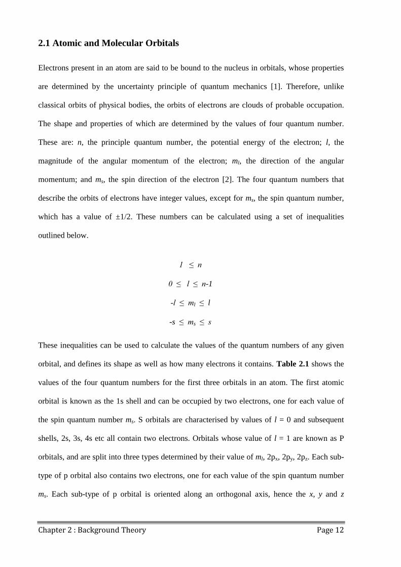
2.1 Atomic and Molecular Orbitals
Electrons present in an atom are said to be bound to the nucleus in orbitals, whose properties
are determined by the uncertainty principle of quantum mechanics [1]. Therefore, unlike
classical orbits of physical bodies, the orbits of electrons are clouds of probable occupation.
The shape and properties of which are determined by the values of four quantum number.
These are: n, the principle quantum number, the potential energy of the electron; l, the
magnitude of the angular momentum of the electron; ml, the direction of the angular
momentum; and ms, the spin direction of the electron [2]. The four quantum numbers that
describe the orbits of electrons have integer values, except for ms, the spin quantum number,
which has a value of ±1/2. These numbers can be calculated using a set of inequalities
outlined below.
1 ≤ n
0 ≤ l ≤ n-1
-l ≤ ml ≤ l
-s ≤ ms ≤ s
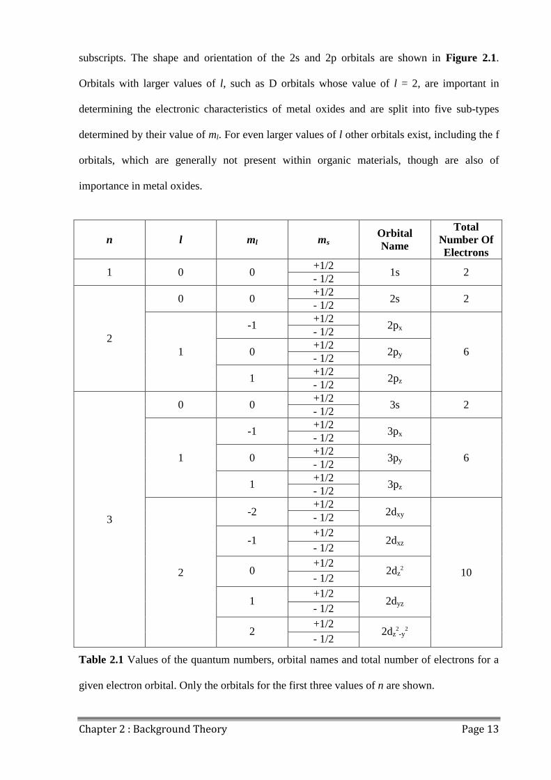
These inequalities can be used to calculate the values of the quantum numbers of any given
orbital, and defines its shape as well as how many electrons it contains. Table 2.1 shows the
values of the four quantum numbers for the first three orbitals in an atom. The first atomic
orbital is known as the 1s shell and can be occupied by two electrons, one for each value of
the spin quantum number ms. S orbitals are characterised by values of l = 0 and subsequent
shells, 2s, 3s, 4s etc all contain two electrons. Orbitals whose value of l = 1 are known as P
orbitals, and are split into three types determined by their value of ml, 2px, 2py, 2pz. Each sub-
type of p orbital also contains two electrons, one for each value of the spin quantum number
ms. Each sub-type of p orbital is oriented along an orthogonal axis, hence the x, y and z
Chapter 2 : Background Theory Page 13
subscripts. The shape and orientation of the 2s and 2p orbitals are shown in Figure 2.1.
Orbitals with larger values of l, such as D orbitals whose value of l = 2, are important in
determining the electronic characteristics of metal oxides and are split into five sub-types
determined by their value of ml. For even larger values of l other orbitals exist, including the f
orbitals, which are generally not present within organic materials, though are also of
importance in metal oxides.
n l ml ms Orbital
Name
Total
Number Of
Electrons
1 0 0 +1/2
1s 2 - 1/2
2
0 0 +1/2
2s 2 - 1/2
1
-1 +1/2
2px
6
- 1/2
0 +1/2
2py - 1/2
1 +1/2
2pz - 1/2
3
0 0 +1/2
3s 2 - 1/2
1
-1 +1/2
3px
6
- 1/2
0 +1/2
3py - 1/2
1 +1/2
3pz - 1/2
2
-2 +1/2
2dxy
10
- 1/2
-1 +1/2
2dxz - 1/2
0 +1/2
2dz2
- 1/2
1 +1/2
2dyz - 1/2
2 +1/2
2dz2-y
2 - 1/2
Table 2.1 Values of the quantum numbers, orbital names and total number of electrons for a
given electron orbital. Only the orbitals for the first three values of n are shown.

Chapter 2 : Background Theory Page 14
Figure 2.1 Shape and orientation of the (a) 2s and (b) 2p orbitals surrounding an atomic
nucleus.
2.2 Orbital Hybridization
When two atoms are brought into close enough proximity, covalent bonds can be formed.
This occurs when the electron orbitals of the two atoms overlap and form molecular orbitals,
which are the combination of the overlapping original electron orbitals. For example, in
hydrogen atoms, which consist of a single proton surrounded by a single electron in the 1s
shell, covalent bonding occurs between two hydrogen atoms to form a diatomic hydrogen
molecule, H2. The orbitals that are formed as a result of this bonding are known as 'bonding
orbitals' and are shown in Figure 2.2.
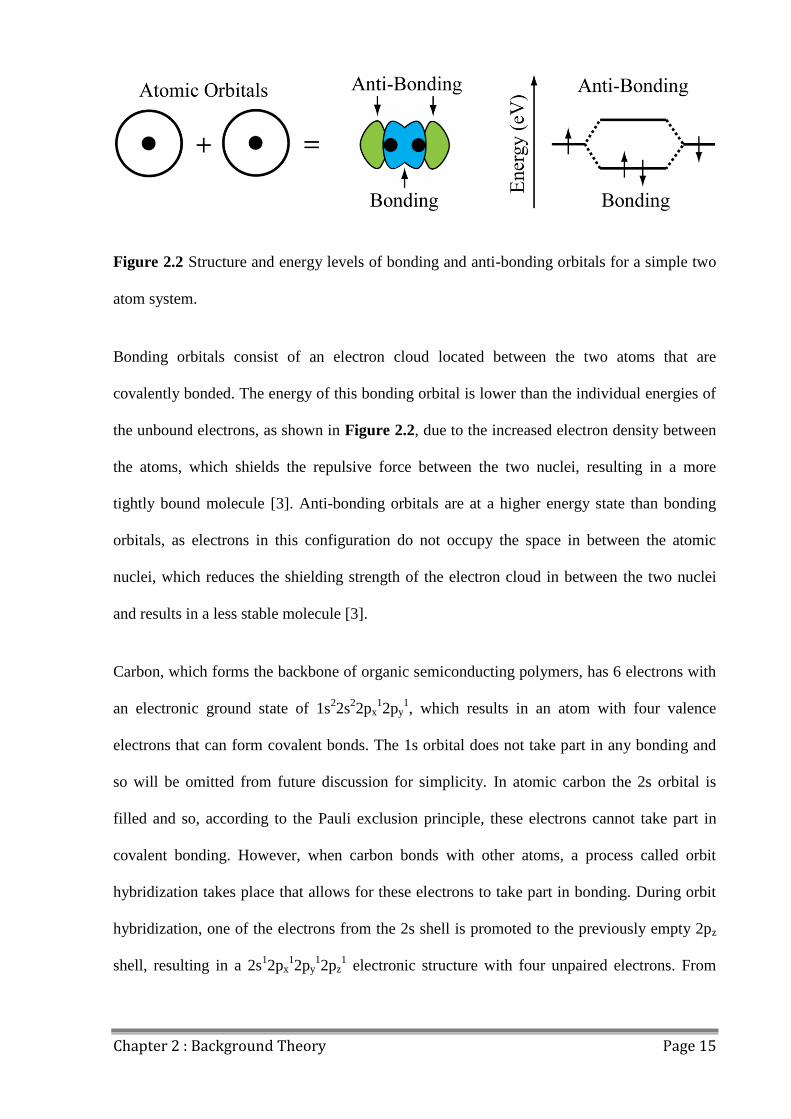
Chapter 2 : Background Theory Page 15
Figure 2.2 Structure and energy levels of bonding and anti-bonding orbitals for a simple two
atom system.
Bonding orbitals consist of an electron cloud located between the two atoms that are
covalently bonded. The energy of this bonding orbital is lower than the individual energies of
the unbound electrons, as shown in Figure 2.2, due to the increased electron density between
the atoms, which shields the repulsive force between the two nuclei, resulting in a more
tightly bound molecule [3]. Anti-bonding orbitals are at a higher energy state than bonding
orbitals, as electrons in this configuration do not occupy the space in between the atomic
nuclei, which reduces the shielding strength of the electron cloud in between the two nuclei
and results in a less stable molecule [3].
Carbon, which forms the backbone of organic semiconducting polymers, has 6 electrons with
an electronic ground state of 1s22s
22px
12py
1, which results in an atom with four valence
electrons that can form covalent bonds. The 1s orbital does not take part in any bonding and
so will be omitted from future discussion for simplicity. In atomic carbon the 2s orbital is
filled and so, according to the Pauli exclusion principle, these electrons cannot take part in
covalent bonding. However, when carbon bonds with other atoms, a process called orbit
hybridization takes place that allows for these electrons to take part in bonding. During orbit
hybridization, one of the electrons from the 2s shell is promoted to the previously empty 2pz
shell, resulting in a 2s12px
12py
12pz
1 electronic structure with four unpaired electrons. From
Chapter 2 : Background Theory Page 16
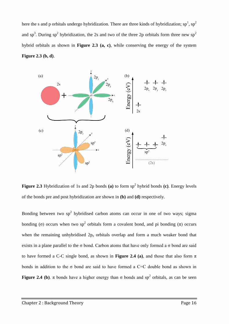
here the s and p orbitals undergo hybridization. There are three kinds of hybridization; sp1, sp
2
and sp3. During sp
2 hybridization, the 2s and two of the three 2p orbitals form three new sp
2
hybrid orbitals as shown in Figure 2.3 (a, c), while conserving the energy of the system
Figure 2.3 (b, d).
Figure 2.3 Hybridization of 1s and 2p bonds (a) to form sp2 hybrid bonds (c). Energy levels
of the bonds pre and post hybridization are shown in (b) and (d) respectively.
Bonding between two sp2 hybridised carbon atoms can occur in one of two ways; sigma
bonding (σ) occurs when two sp2 orbitals form a covalent bond, and pi bonding (π) occurs
when the remaining unhybridised 2pz orbitals overlap and form a much weaker bond that
exists in a plane parallel to the σ bond. Carbon atoms that have only formed a σ bond are said
to have formed a C-C single bond, as shown in Figure 2.4 (a), and those that also form π
bonds in addition to the σ bond are said to have formed a C=C double bond as shown in
Figure 2.4 (b). π bonds have a higher energy than σ bonds and sp2 orbitals, as can be seen
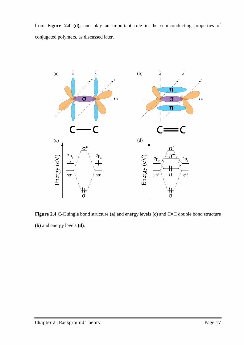
Chapter 2 : Background Theory Page 17
from Figure 2.4 (d), and play an important role in the semiconducting properties of
conjugated polymers, as discussed later.
Figure 2.4 C-C single bond structure (a) and energy levels (c) and C=C double bond structure
(b) and energy levels (d).
Chapter 2 : Background Theory Page 18
2.3 Conjugation
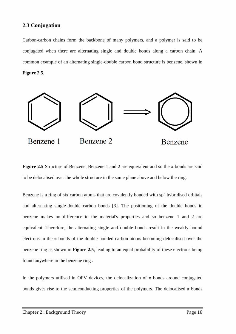
Carbon-carbon chains form the backbone of many polymers, and a polymer is said to be
conjugated when there are alternating single and double bonds along a carbon chain. A
common example of an alternating single-double carbon bond structure is benzene, shown in
Figure 2.5.
Figure 2.5 Structure of Benzene. Benzene 1 and 2 are equivalent and so the π bonds are said
to be delocalised over the whole structure in the same plane above and below the ring.
Benzene is a ring of six carbon atoms that are covalently bonded with sp2 hybridised orbitals
and alternating single-double carbon bonds [3]. The positioning of the double bonds in
benzene makes no difference to the material's properties and so benzene 1 and 2 are
equivalent. Therefore, the alternating single and double bonds result in the weakly bound
electrons in the π bonds of the double bonded carbon atoms becoming delocalised over the
benzene ring as shown in Figure 2.5, leading to an equal probability of these electrons being
found anywhere in the benzene ring .
In the polymers utilised in OPV devices, the delocalization of π bonds around conjugated
bonds gives rise to the semiconducting properties of the polymers. The delocalised π bonds
Chapter 2 : Background Theory Page 19
form the highest occupied molecular orbital (HOMO) level of the polymer, with the higher
energy unoccupied π* anti-bonding orbital forming the lowest unoccupied molecular orbital
(LUMO) level, as shown in Figure 2.4 (d); promoting an electron from the HOMO level to
the LUMO level changes the electronic structure of the molecule from bonding to anti-
bonding. The HOMO and LUMO levels of semiconducting polymers can be compared to the
valence and conduction bands in inorganic semiconductors, and the difference between the
HOMO and LUMO energy levels is defined as the material's energy gap. These energy levels
are not only affected by the individual atoms but also by the surrounding environment due to
other electronic interactions. Within tightly packed amorphous films, conjugated polymer
energy levels are shifted due to a property known as energetic disorder [4], [5], though this
effect is reduced in more ordered and crystalline materials.
Varying the components of a conjugated polymer chain can affect the HOMO and LUMO
levels of the material, which can be utilised to tune the energy gap of the material and its
charge transport properties. Polymers used for OPV applications tend to have an electron
'donor' component that is electron rich, and an electron 'accepting' component that is electron
poor. Changing these components, or even just individual atoms, can affect these electron rich
or poor areas, resulting in modified energy levels [6]–[10].
2.4 Photophysics of Organic Conjugated Polymers
Conjugated polymers are able to absorb photons in the visible region of the solar spectrum
due their energy gap, which can be engineered by making atomic or component substitutions
to the polymer as covered in 2.3 Conjugation. This process is critical to polymer design for
OPV devices, as it determines the range of wavelengths that the polymer can absorb.
Chapter 2 : Background Theory Page 20
2.4.1 Exciton Formation
The process of photon absorption promotes an electron from the HOMO level of the polymer
to the LUMO level as long as the energy of the photon equals or exceeds the energy gap
between these two levels. If the energy of the photon is sufficiently high, an electron is
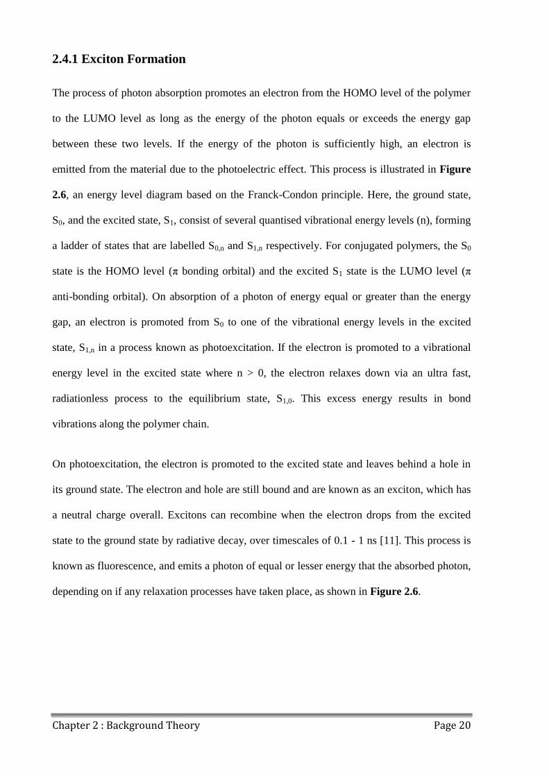
emitted from the material due to the photoelectric effect. This process is illustrated in Figure
2.6, an energy level diagram based on the Franck-Condon principle. Here, the ground state,
S0, and the excited state, S1, consist of several quantised vibrational energy levels (n), forming
a ladder of states that are labelled S0,n and S1,n respectively. For conjugated polymers, the S0
state is the HOMO level (π bonding orbital) and the excited S1 state is the LUMO level (π
anti-bonding orbital). On absorption of a photon of energy equal or greater than the energy
gap, an electron is promoted from S0 to one of the vibrational energy levels in the excited
state, S1,n in a process known as photoexcitation. If the electron is promoted to a vibrational
energy level in the excited state where n > 0, the electron relaxes down via an ultra fast,
radiationless process to the equilibrium state, S1,0. This excess energy results in bond
vibrations along the polymer chain.
On photoexcitation, the electron is promoted to the excited state and leaves behind a hole in
its ground state. The electron and hole are still bound and are known as an exciton, which has
a neutral charge overall. Excitons can recombine when the electron drops from the excited
state to the ground state by radiative decay, over timescales of 0.1 - 1 ns [11]. This process is
known as fluorescence, and emits a photon of equal or lesser energy that the absorbed photon,
depending on if any relaxation processes have taken place, as shown in Figure 2.6.

Chapter 2 : Background Theory Page 21
Figure 2.6 Franck-Condon energy level diagram for S0 and S1 energy levels with absorption,
fluorescence and radiationless relaxation.
In comparison to inorganic semiconductors, conjugated polymers have a low dielectric
constant, usually between 3 - 4 [12], [13], and so the charges that are generated on
photoexcitation are not shielded from each other. This leads to a situation where the generated
excitons are still strongly bound together by coulombic forces in a state known as an Frenkel
excitons with a binding energy of ~ 0.3 eV [13]–[15].
Chapter 2 : Background Theory Page 22
2.4.2 Exciton Diffusion and Dissociation
Frenkel excitons cannot be dissociated thermally, as is the case for excitons in inorganic
semiconductors, due to their strong binding energy. Dissociation can only occur at an
interface between the conjugated polymer, henceforth referred to as the donor, and another
material known as an electron acceptor [14]. However, the exciton must diffuse to this
interface before recombination occurs. The efficiency of exciton diffusion is known as the
diffusion co-efficient, D, and the distance an exciton can travel before recombination is
known as the exciton diffusion length (LD). The relationship between these two parameters is
given in Equation 2.1 below.
Equation 2.1
Where τ is the photoluminescence decay lifetime of the excitons. If the average distance
between the donor and acceptor interfaces are ≤ LD then it is likely that the excitons will be
dissociated into free charges at the interface. For conjugated polymers, the diffusion length is
of the order of 10 nm [14]. If the exciton does not reach a donor-acceptor interface in time,
geminate recombination occurs (where an electron and hole from the same exciton
recombine), often with an associated photoluminescence. In OPV devices, this short diffusion
length is overcome by the morphology of the donor-acceptor blend film, in which the two
materials are intermixed at a similar length scale; a subject discussed in more detail in 2.5
Device Architecture. The donor-acceptor blend film is also known as the 'active layer' of an
OPV device.
Dissociation itself is the process by which the bound electron-hole pair (the exciton) is
separated into free charge carriers. This process occurs at the interface between the
conjugated polymer, the donor, and an acceptor material, providing the energy transfer is
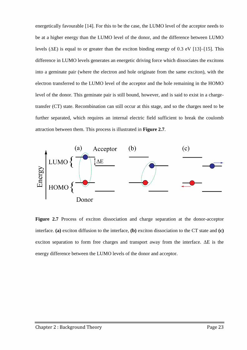
Chapter 2 : Background Theory Page 23
energetically favourable [14]. For this to be the case, the LUMO level of the acceptor needs to
be at a higher energy than the LUMO level of the donor, and the difference between LUMO
levels (ΔE) is equal to or greater than the exciton binding energy of 0.3 eV [13]–[15]. This
difference in LUMO levels generates an energetic driving force which dissociates the excitons
into a geminate pair (where the electron and hole originate from the same exciton), with the
electron transferred to the LUMO level of the acceptor and the hole remaining in the HOMO
level of the donor. This geminate pair is still bound, however, and is said to exist in a charge-
transfer (CT) state. Recombination can still occur at this stage, and so the charges need to be
further separated, which requires an internal electric field sufficient to break the coulomb
attraction between them. This process is illustrated in Figure 2.7.
Figure 2.7 Process of exciton dissociation and charge separation at the donor-acceptor
interface. (a) exciton diffusion to the interface, (b) exciton dissociation to the CT state and (c)
exciton separation to form free charges and transport away from the interface. ΔE is the
energy difference between the LUMO levels of the donor and acceptor.
Chapter 2 : Background Theory Page 24
2.4.3 Charge Transport
After the exciton has been dissociated, the free charges need to be transported through the
donor and acceptor molecules to the electrodes for extraction. This process is facilitated by
the delocalization of the HOMO and LUMO energy levels of the materials. However, energy
level delocalization can only occur between states of equal energy, and so distortion in energy
levels due to local effects, as discussed in 2.3 Conjugation, results in separate localised states
along the polymer chains. It is the charge transport between these localised states that
determines the mobility of charge carriers in the conjugated polymers [4], and it is agreed that
a hopping transport process is the dominant mechanism of charge transport through these
localised states. This hopping process is dependent on both the energetic disorder of the
localised states and also the distance between the hopping sites [4], [16]. Charges hop from
one site to the next by tunnelling through the potential barrier separating the two sites. The
barrier energy, and therefore the probability of the tunnelling taking place, is determined by
differences in energy and location of the two sites. For charge carrier mobility to be improved,
both of these parameters needs to be reduced as much as possible; a process that can be
achieved through modifications to the chemical structure and processing conditions of the
materials. Increasing conjugation length in the donor polymers, or decreasing the distance
between charge transport sites between monomers, can decrease the distance between
hopping sites [17], [18], and the intermolecular distance can be decreased by improving the
polymer-polymer stacking in a film by improving the molecular crystallinity [19].
Chapter 2 : Background Theory Page 25
2.4.4 Charge Extraction
Upon exciton dissociation, separation and transport through the active layer, charge extraction
may take place at the electrical contacts. This efficiency of this process is dependent on the
work function (WF) of the contact materials matching the energy levels of the donor-acceptor
materials, allowing for charge transport across the interface. In an ideal situation, the device
electrodes should follow the rules below:
Equation 2.2
Equation 2.3
Here, the WF of the anode is matched to the energy of the HOMO level of the donor for the
extraction of holes, and the WF of the cathode is matched to the energy of the LUMO level of
the acceptor for extraction of electrons. These interfaces, when matched in energy in such a
way, are known as ohmic contacts.
However, the interfaces in OPVs are rarely so simple due to the wide variety of materials
used. Metal oxides have both valence and conduction bands, and a Fermi level in the energy
gap. When initially comparing materials against one another the vacuum level is aligned, as
shown in Figure 2.8, but this depiction of energy levels only holds true when the materials
are not in electrical contact with one another. When materials are brought into electrical
contact, Fermi level alignment can occur under certain conditions, where the Fermi levels of
the two materials equalize [20]. It is this Fermi level alignment that allows for efficient charge
transfer across such interfaces.
The simplest example of Fermi level alignment is the metal-metal interface, as shown in
Figure 2.8 (a). In this instance, electrons flow from the metal with the highest WF to the
Chapter 2 : Background Theory Page 26
lower WF metal. For metal-organic contacts, the Fermi levels can align in one of two ways; if
the WF of the metal is equal to or lower than the upper critical Fermi level (ΦP) level of the
organic material, LUMO alignment occurs, and if the WF of the metal is equal to or higher
than the lower critical Fermi level (ΦN) of the organic material, HOMO alignment occurs,
shown in Figure 2.8 (b), (c) respectively. If the WF of the metal is between these two values
then the Fermi levels will not align and the materials will remain vacuum level aligned [21],
which is detrimental to charge transport across the interface.
Energy level alignment at interfaces is critical to device performance, as poor alignment can
lead to charge transfer losses due to barriers forming that inhibit extraction [22], [23]. Ohmic
contacts form when there is no barrier to extraction due to well aligned energy levels, and
Schottky-Mott contacts are formed when there is an energy barrier present. Charge transfer
can still occur in Schottky-Mott contacts, but at the cost of device efficiency resulting from an
increase in device series resistance.
In OPV devices, anode and cathode buffer layers are used to improve the energy level
alignment between the active layer and the electrical contacts, and thereby improve device
performance. Not only do these layers reduce the energy barrier for charge extraction and
reduce charge leakage [24], [25], but they can also provide protection from ingress of oxygen
and moisture into the active layer, which can cause degradation in performance (discussed in
more detail in 2.9 OPV Stability and Degradation). The buffer layer in between the active
layer and the anode is known as the hole transport layer (HTL) and the buffer layer at the
cathode is known as the electron transport layer (ETL). These buffer layer materials are
covered in more detail in 2.6 Interface Materials.

Chapter 2 : Background Theory Page 27
Figure 2.8 Energy level alignment pre and post contact for various interfaces. (a) metal-metal
(b) metal-organic for LUMO level alignment and (c) metal-organic for HOMO level
alignment. Evacuum is the vacuum energy level, ΦM(1,2) is the metal work function, ΦP is the
upper critical Fermi level and ΦN is the lower critical Fermi level.
The alignment of energy levels on contact in an OPV device results in a built-in potential
(Vbi) which dictates the direction of flow for charge carriers. Under open-circuit conditions,
the open circuit voltage (Voc) that results from the energy level alignment is determined from
the energy levels of the donor and acceptor materials as in Equation 2.4.
Chapter 2 : Background Theory Page 28
Equation 2.4
Where E is the energy of the corresponding energy levels of the donor and acceptor materials,
e is the elementary charge, and 0.3 V is an empirical factor that accounts for the difference in
Voc and Vbi. This empirical factor has also been shown to be due to the binding energy of the
Frenkel excitons [26]. Several other factors can affect Voc in OPV devices, including
recombination [27], light intensity [28], [29], charge transfer states [30] and device
morphology [31], [32].
2.5 Device Architecture
OPV device architecture has evolved since its inception, when Ghosh et al. deposited an
active layer of tetracene between aluminium and gold contacts in 1973 [33]. This device had
an efficiency of only 10-4
%, but was further enhanced to 0.7% by replacing the tetracene with
a merocyanine dye [34]. This single layer device was restricted in performance by a variety of
factors, not least the lack of an electron accepting molecule and interfacial buffer layers.
From this single layer structure, the bilayer (or heterojunction) architecture was developed,
where two materials were deposited on top of one another, which created an interface at
which excitons could be dissociated. The first materials used were copper phthalocynanine
(CuPc) and a perylene tetracarboxylic (PV) derivative, with an efficiency of 1% achieved in
1986 [35]. The use of indium tin oxide (ITO) as the anode contact material was also a
significant advance, and this transparent conducting metal oxide is used in the majority of
OPV devices to this day.
Chapter 2 : Background Theory Page 29
As previously mentioned in 2.4.2 Exciton Diffusion and Dissociation, excitons in OPVs
need to be dissociated within ~ 10 nm of generation before geminate recombination occurs.
The bilayer structure, although it resulted in an increase in device efficiency compared to
previous efforts, still resulted in significant losses due to recombination, as there was only one
interface between the two materials. This problem was addressed with the introduction of the
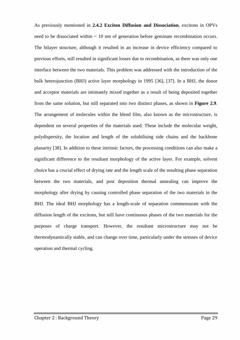
bulk heterojunction (BHJ) active layer morphology in 1995 [36], [37]. In a BHJ, the donor
and acceptor materials are intimately mixed together as a result of being deposited together
from the same solution, but still separated into two distinct phases, as shown in Figure 2.9.
The arrangement of molecules within the blend film, also known as the microstructure, is
dependent on several properties of the materials used. These include the molecular weight,
polydispersity, the location and length of the solubilising side chains and the backbone
planarity [38]. In addition to these intrinsic factors, the processing conditions can also make a
significant difference to the resultant morphology of the active layer. For example, solvent
choice has a crucial effect of drying rate and the length scale of the resulting phase separation
between the two materials, and post deposition thermal annealing can improve the
morphology after drying by causing controlled phase separation of the two materials in the
BHJ. The ideal BHJ morphology has a length-scale of separation commensurate with the
diffusion length of the excitons, but still have continuous phases of the two materials for the
purposes of charge transport. However, the resultant microstructure may not be
thermodynamically stable, and can change over time, particularly under the stresses of device
operation and thermal cycling.
Chapter 2 : Background Theory Page 30
Figure 2.9 BHJ morphology. Red lines represent the donor polymer molecules and black
circles represent acceptor molecules.
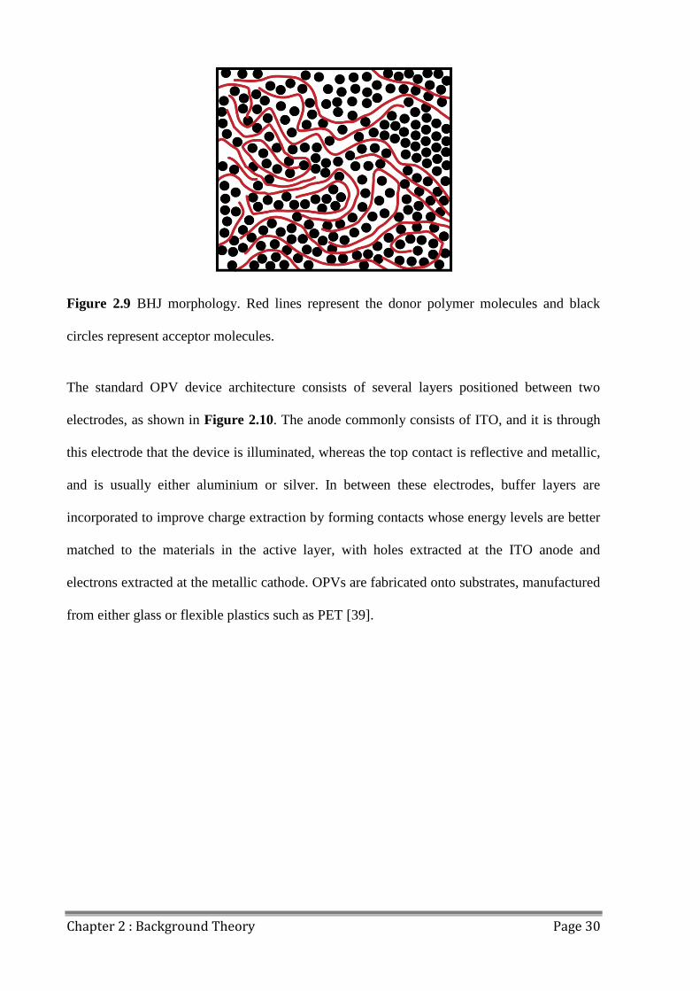
The standard OPV device architecture consists of several layers positioned between two
electrodes, as shown in Figure 2.10. The anode commonly consists of ITO, and it is through
this electrode that the device is illuminated, whereas the top contact is reflective and metallic,
and is usually either aluminium or silver. In between these electrodes, buffer layers are
incorporated to improve charge extraction by forming contacts whose energy levels are better
matched to the materials in the active layer, with holes extracted at the ITO anode and
electrons extracted at the metallic cathode. OPVs are fabricated onto substrates, manufactured
from either glass or flexible plastics such as PET [39].
Chapter 2 : Background Theory Page 31
Figure 2.10 Standard architecture of OPVs as fabricated onto ITO coated substrates. Six
pixels on the substrate are defined by the overlap of the electrodes and are outlined by red
dotted lines.
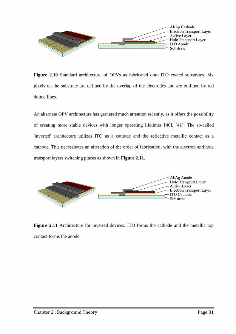
An alternate OPV architecture has garnered much attention recently, as it offers the possibility
of creating more stable devices with longer operating lifetimes [40], [41]. The so-called
'inverted' architecture utilizes ITO as a cathode and the reflective metallic contact as a
cathode. This necessitates an alteration of the order of fabrication, with the electron and hole
transport layers switching places as shown in Figure 2.11.
Figure 2.11 Architecture for inverted devices. ITO forms the cathode and the metallic top
contact forms the anode.
Chapter 2 : Background Theory Page 32
2.6 Interface Materials
Interface materials play an important role in the performance of OPV devices as previously
mentioned, improving the energy level alignment at the interfaces between the active layer
materials and the electrical contacts. Interface materials come in two different general forms,
hole transport layers (HTLs) and electron transport layers (ETLs); HTLs improve hole
extraction and at the anode and ETLs improve electron extraction at the cathode. They also
reduce charge leakage at the contacts by blocking unwanted charge transfer (electrons for the
HTL and holes at the ETL). The following two sections cover the interface materials used in
this thesis.
2.6.1 PEDOT:PSS
One of the most commonly used HTL layers is PEDOT:PSS, a mix of two polymers; the
insoluble PEDOT, and PSS. With the addition of PSS, the PEDOT:PSS mixture becomes
water soluble [42], and thin films can easily be processed from solution that exhibit several
characteristics that are desirable for OPV interlayers: high conductivity, good film
transparency and high charge carrier mobility [43]. The most commonly used PEDOT:PSS
solution for OPV applications, Heraeus Clevios™ P VP AI 4083, has a ratio of 1:6 PEDOT to
PSS, and a conductivity of the order of 10-3
Scm-1
[42]. PEDOT:PSS has a work function of ~
5.2 eV [42], [44], and when used as a HTL between ITO and the active layer of OPVs, aids
extraction of holes across the interface. This is achieved by planarising the surface of the ITO
[45], reducing the number of shorts and inhomogeneities formed at the interface, and
increasing the work function of the ITO anode; allowing energy level matching with the
donor polymer in the active layer. Thin films of PEDOT:PSS are extremely hygroscopic [44],
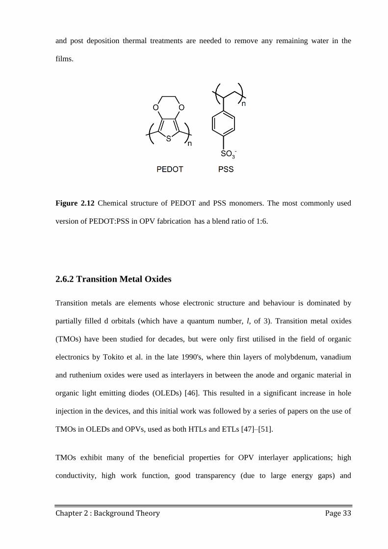
Chapter 2 : Background Theory Page 33
and post deposition thermal treatments are needed to remove any remaining water in the
films.
Figure 2.12 Chemical structure of PEDOT and PSS monomers. The most commonly used
version of PEDOT:PSS in OPV fabrication has a blend ratio of 1:6.
2.6.2 Transition Metal Oxides
Transition metals are elements whose electronic structure and behaviour is dominated by
partially filled d orbitals (which have a quantum number, l, of 3). Transition metal oxides
(TMOs) have been studied for decades, but were only first utilised in the field of organic
electronics by Tokito et al. in the late 1990's, where thin layers of molybdenum, vanadium
and ruthenium oxides were used as interlayers in between the anode and organic material in
organic light emitting diodes (OLEDs) [46]. This resulted in a significant increase in hole
injection in the devices, and this initial work was followed by a series of papers on the use of
TMOs in OLEDs and OPVs, used as both HTLs and ETLs [47]–[51].
TMOs exhibit many of the beneficial properties for OPV interlayer applications; high
conductivity, high work function, good transparency (due to large energy gaps) and

Chapter 2 : Background Theory Page 34
semiconducting properties. The position of the conduction and valence band energy levels of
the TMOs used in this thesis are shown below in Figure 2.13 in comparison to ITO,
PEDOT:PSS and calcium.
Figure 2.13 Energy levels for ITO [52], PEDOT:PSS [42], [44], MoOx (molybdenum oxide)
[53], V2Ox (vanadium oxide) [53], TiOx (titanium oxide) [51], and Ca (calcium). For the
TMOs, the energy levels quoted are for freshly evaporated films that have not been exposed
to oxygen or moisture. The materials can be grouped into two categories, HTL materials
(MoOx, V2Ox and PEDOT:PSS) and ETL materials (TiOx and Ca).
Chapter 2 : Background Theory Page 35
2.7 Active Layer Materials
Research into polymers for use in photovoltaics began in earnest in the 1970's and 1980's,
fuelled by an interest in exploiting the natural organic compounds used in photosynthesis and
the use of organic photoconductors in Xerographic photocopying. Initially the rather modest
aims of the field were to find chemically stable materials with good optical absorption, and so
the first materials to be used were merocyanine and phthalocyanine dyes [35], [54], the
structures of which are shown in Figure 2.14 (a), (b) respectively. These materials could be
deposited either by thermal evaporation or solution deposition to form thin films on
conducting substrates, but only resulted in power conversion efficiencies of around 1% [35] at
best.
The aspiration of the field (to achieve low cost, large area, flexible OPV modules) required
the use of soluble materials that could be deposited using simple solution based methods.
Polymer semiconductors were quickly earmarked as the most promising material technology;
the ability to tailor the materials solubility, optical and electronic properties (including the
HOMO and LUMO energy levels, and therefore the optical bandgap) closely met the
demands of large scale OPV production. Although initial performance for polymer
semiconductors in OPVs was rather unimpressive, the first generation of high solubility
polymers such as polyphenylenevinylenes (PPV), and their derivatives, marked a milestone in
OPV development. However, in pristine polymer semiconductors the charge generation
efficiency was of the order of 0.1% due to the nature of the strongly bound Frenkel excitons,
and the charge separation mechanism was driven largely by the presence of defects or
impurities [55]. A major breakthrough in the field was made when polymer semiconductors
were combined with another material having a high electron affinity, an acceptor, which

Chapter 2 : Background Theory Page 36
allowed for charge separation of the bound excitons in the polymer at the interface between
the two materials.
Figure 2.14 Chemical structures of the dyes (a) merocyanine, (b) phthalocyanine and the
polymers (c) MEH-PPV, (d) MDMO-PPV and (e) P3HT.
This approach led directly to the development of the BHJ device, as the intermixing of the
two materials resulted in more charge separation at interfaces throughout the active layer. The
first BHJ architecture OPV devices, developed in 1995, showed efficiencies of 2.9% [37] (for
monochromatic light, not the now standard AM1.5), and were based on a MEH-PPV:PC60BM
(poly(2-methoxy-5-(2′-ethyl-hexyloxy)-1,4-phenylenevinylene):Phenyl-C61-butyric acid
methyl ester) active layer. The structure of MEH-PPV is shown in Figure 2.14 (c). This was
also the first instance of PCBM being used as an acceptor in an OPV. Remarkably, after 17
Chapter 2 : Background Theory Page 37
years, PCBM is still the most widely used acceptor material in BHJ OPV devices due to its
high solubility, favourable energy levels and performance, a subject that is covered in more
detail in 2.7.2 Fullerenes.
In 2001, Shaheen et al showed that the efficiency of a BHJ OPV based on another PPV
derivative, MDMO-PPV (structure shown in Figure 2.14 (d)), and PCBM was drastically
affected by the active layer morphology [56]. By optimizing the BHJ morphology of the
active layer through careful choice of solvents, a device efficiency of 2.5% under AM1.5
illumination was achieved - an almost threefold increase over any previously reported device
efficiencies.
Unfortunately, the relatively large bandgap of PPV type polymers, in combination with their
limited charge transport mobility, led to maximum attainable efficiencies of around 3%.
Considering that commercial applications require efficiencies around 10%, this limitation
provided the impetus to develop the next generation of semiconducting polymers. Poly(3-
hexylthiophene) (P3HT), whose structure shown in Figure 2.14 (e), and other poly-alkyl-
thiophenes emerged as a promising next step. P3HT was one of the first conjugated polymers
studied for use in OPVs, but it was only with the discovery of the effect of post-production
thermal treatments that device efficiencies of around 3.5% were reported [57]. This
development led to P3HT becoming the new workhorse of OPV development, facilitated by
the wide availability of the polymer from multiple manufacturers as the structure was not
patented. The efficiency of P3HT:PCBM based OPV devices quickly rose to around 5% [19]
due to improvements in polymer regioregularity [58] and molecular weight, optimizing the
annealing temperature [19] and reducing interface losses.
Chapter 2 : Background Theory Page 38
However, as with the PPV based polymer systems, the limitations of P3HT were quickly
discovered. P3HT has excellent absorption and charge transport properties, and as such an
active layer of between 100 - 200nm absorbs most incident light and results in fill factors of
around 70% [59]. Unfortunately, the energy levels of P3HT are not well suited to PCBM, and
so the highest reported values for Voc were around 0.66V [60].
The most recent improvements in polymer:fullerene solar cell efficiencies and stabilities have
largely come from the synthesis of new polymers which have lower lying HOMO levels and
smaller band gaps. A lower lying HOMO level has the twin benefit of allowing more of the
energy of each photon to be harvested due to better energy alignment to PCBM [15], whilst
also improving the chemical stability of the material by making oxidation more difficult. As
such, there has been a recent trend in the development of polymers having a lower lying
HOMO levels in the region of -5.10eV to -5.50eV, such as PCDTBT (poly[9-(heptadecan-9-
yl)-9H-carbazole-2,7-diyl-alt-(4′,7′-di-2-thienyl-2′,1′,3′-benzothiadiazole)-5,5-diyl]) [61] and
PTB7 (poly({4,8-bis[(2-ethylhexyl)oxy]benzo[1,2-b:4,5-b′]dithiophene-2,6-diyl}{3-fluoro-2-
[(2-ethylhexyl)carbonyl]thieno[3,4-b]thiophenediyl})) [62].
One family of polymers that have attracted a lot of interest in recent years for OPV
applications are the carbazole co-polymers. The most commonly studied carbazole co-
polymer, PCDTBT, has achieved device efficiencies of 7.2% [63]. Several studies of this
polymer have optimising the device structure [25], [50], [64]–[66] and characterised device
stability and degradation pathways [61], [67], [68], with extrapolated lifetimes of up to 10
years reported [68]; all of which make it an attractive proposition for efficient, stable OPV
material. The structure of PCDTBT can be altered to improve its solubility in common
organic solvents such as chloroform, chlorobenzene and dichlorobenzene by the addition of
an octyloxy substituent on the benzothiadiazole acceptor unit [69]. The resulting polymer has

Chapter 2 : Background Theory Page 39
increased solubility while maintaining high device performance when blended with a PC70BM
acceptor [69]. Extra thiophene moieties can also be added along the polymer backbone, which
redshift the absorption through a reduction in the optical energy gap by increasing the
intramolecular charge transfer along the polymer backbone [70]. Other substitutions can also
be carried out to alter the HOMO and LUMO energy levels and bandgap of PCDTBT; the
thiophene units can be replaced with selenophenes to improve the charge carrier mobility
through enhanced interchain interactions [71], and the carbazole unit can be replaced with a
polyfluorene unit which has enhanced thermal and chemical stability [72]–[75]. The chemical
structures of these polymers and the moieties that they consist of are included 2.7.1 Polymer
List.
2.7.1 Polymer List
The following is a list of the chemical names and structures of all the polymers used within
this thesis.
PCDTBT
Figure 2.15 PCDTBT - Poly[N-9’-heptadecanyl-2,7-carbazole-alt-5,5-(4’,7’-di-2-thienyl-
2’,1’,3’- benzothiadiazole)]
Chapter 2 : Background Theory Page 40
PCDTBT-8
Figure 2.16 PCDTBT-8 - poly[9-(heptadecan-9-yl)-9H-carbazole-2,7-diyl-alt-(5,6-
bis(octyloxy)-4,7-di(thiophen-2-yl)benzo[c][1,2,5]thiadiazole)-5,5-diyl] - the addition of an
octyloxy substituent on the benzothiadiazole of PCDTBT improves the solubility of the
polymer [69].
PCDSeBT-8
Figure 2.17 PCDSeBT-8 - (poly[9-(heptadecan-9-yl)-9H-carbazole-2,7-diyl-alt-(5,6-
bis(octyloxy)-4,7-di(selenophen-2-yl)benzo[c][1,2,5]thiadiazole-5,5-diyl]). The same
chemical structure as PCDTBT-8, but with the thiophenes replaced with selenophenes.
Chapter 2 : Background Theory Page 41
PFDT2BT-8
Figure 2.18 PFDT2BT-8 - (poly[9,9-dioctylfl u- orene-4,7-alt-(5,6-bis(octyloxy)-4,7-di(2,2′-
bithiophen-5-yl) benzo[c][1,2,5]thiadiazole)-5,5-diyl]) - a fluorene replaces the carbazole in
PCDTBT-8, with an extra thiophene on either side of the benzothiadiazole.
PTB7
Figure 2.19 PTB7 - (poly({4,8-bis[(2-ethylhexyl)oxy]benzo[1,2-b:4,5-b′]dithiophene-2,6-
diyl}{3-fluoro-2-[(2-ethylhexyl)carbonyl]thieno[3,4-b]thiophenediyl})). A high efficiency
polymer that has achieved PCEs of 9.2% with an inverted device architecture [76].

Chapter 2 : Background Theory Page 42
Figure 2.20 HOMO and LUMO energy levels for the above polymers. Data for PCDTBT and
analogues acquired by Department of Chemistry, University of Sheffield by cyclic
voltametry. Data for PTB7 from [62].
2.7.2 Fullerenes
PC60BM and its variants are the ubiquitous electron accepting material, found in the vast
majority of OPV devices. Based on a buckminsterfullerene [77], a spherical cage of sixty
carbon atoms with a solubilising methyl ester group attached, as shown in Figure 2.21 (a), it
offers several physical and electrical characteristics that make it a near perfect electron
accepting material. When paired with organic polymers, photoinduced charge transfer from
the polymer to the fullerene is extremely fast and efficient [78], and it has a very high electron
mobility [79]. The LUMO level energy of PC60BM is - 4.3eV [25], making it an excellent
match for many polymers, crucially having the required energy difference between LUMO
levels of greater than 0.3 eV to allow for exciton dissociation.
Another form of PCBM that has also been used as an electron acceptor material utilises a
buckminsterfullerene with 70 carbon atoms, and as such is known as PC70BM, shown in
Figure 2.21 (b). Due to the lack of spherical symmetry in the C70 fullerene, an increase in
absorption co-efficient over the visible range of the solar spectrum is observed [80]. This is
Chapter 2 : Background Theory Page 43
beneficial to OPV devices, as although the majority of absorption is due to the polymer in
OPVs, the active layer blend is often composed of a significantly larger weight fraction of
PCBM to increase the number of donor-acceptor interfaces throughout the film. Therefore,
the increased light absorption of PC70BM, when compared to PC60BM, increases the charge
generation rate and leads to an enhancement of Jsc, and more therefore efficient devices.
Figure 2.21 Chemical structure of the most commonly used electron acceptor materials, (a)
PC60BM and (b) PC70BM.
2.8 Ambient Processing
Currently, the majority of OPVs are fabricated in nitrogen atmosphere gloveboxes to exclude
oxygen and moisture from the process due to their detrimental effects of device performance
and long-term stability [81]–[83]. However, this is not a feasible situation for the eventual
scale up of production to produce OPV devices for mass manufacturing applications, as it
adds significantly to the embodied energy cost of the devices. An extra degree of complexity
is added in large scale production as most results for OPVs are from small scale, laboratory
produced devices, tested under extremely restrictive conditions. Laboratory devices achieve
Chapter 2 : Background Theory Page 44
high performance through delicate and highly empirical relationships between multiple
fabrication parameters such as solvent choice, drying speeds, active layer and interface
materials and substrate/encapsulation materials. To scale up the fabrication process, which
also involves speeding up the process, requires re-evaluating the inter-relationships between
all these parameters, with added complexity due to processing in ambient conditions.
Currently, attempts to scale up production of OPVs from lab to industrial scale have led to
drops in PCE [84], [85]. Also, the solvents regularly used in OPV fabrication, such as
chlorobenzene and dichlorobenzene, are extremely toxic, and would need to be replaced by
less toxic alternatives in a commercial setting.
There are several reported lab investigations into ambient processing of OPVs, all of which
utilize a P3HT:fullerene active layer system [83], [86], [87]. This is because the degradation
mechanisms and performance of the P3HT:fullerene system are very well understood, and as
such the effects of ambient processing can be separated from other device performance effects
more readily.
Ambient processed devices with a P3HT:PCBM active layer exhibit lower efficiency than
those processed in an inert atmosphere [87]. The loss in device performance is primarily due
to a reduced FF as a result of oxygen doping of the active layer blend. Ambient processing
decreases both hole and electron mobility, with hole transport in P3HT reduced by oxygen
doping introducing trap states in the polymer, and electron mobility is reduced by a factor of ~
2 [83]. However, it has been shown that thermal annealing treatments can successfully reduce
electron and hole trap densities introduced through ambient processing [83].
Chapter 2 : Background Theory Page 45
The most successful fabrication technique so far, in terms of scalability, is roll-to-roll (R2R)
processing. The main principles in roll-to-roll printing are so called 'wet films through contact'
printing, generally used for the top and bottom electrodes, and 'wet films without contact'
printing, used for solution processed layers. Wet films through contact printing is where wet
films of material are transferred from a patterned roller to a substrate via direct contact, as
opposed to without contact printing where there is no contact between the substrate and
depositing apparatus. Multi-layer OPVs are fabricated in one continuous process onto a
flexible poly(ethyleneterephthalate) (PET) sheet with a printed pattern of ITO forming the
bottom electrode. Krebs et al successfully scaled up an inverted device based on a
ITO/ZnO/P3HT:PCBM/PEDOT:PSS/Ag architecture from the laboratory to vacuum free R2R
with little loss in cell efficiency [85]; 2.7% efficient cells for devices fabricated in a lab, and
2.3% for device fabricated using R2R techniques. The ZnO, PEDOT:PSS and active layers
were deposited using normal printing techniques, the top Ag cathode was deposited using
screen-printing techniques and the devices were encapsulated using an acrylic adhesive and
PET foil.
Though R2R printing offers a promising method for producing OPV devices on an industrial
scale, limited device efficiency due to material limitations and short device lifetimes due to
insufficient encapsulation means that further developments are needed before
commercialization is feasible.
Chapter 2 : Background Theory Page 46
2.9 OPV Stability and Degradation
Over the past decade, increased effort has been made to further the understanding of
degradation mechanisms in OPVs and how this affects their operating lifetimes. Extensive
studies of OPVs based on the polymer P3HT have been made [68], [88]–[90], with lifetimes
of up to 3 years reported [68]. More recently, outdoor interlaboratory studies have produced
devices with lifetimes in excess of 5 years [91], and laboratory studies have extrapolated
device lifetimes of up to 10 years for other polymer systems [68], [92].
Much of the early work done on the lifetimes of devices was before the introduction of
standardised methodologies, introduced after the publication of a consensus paper on testing
protocols and the advent of the annual International Summit on OPV Stability (ISOS) [93].
These standardised methodologies have provided a framework for testing procedures and how
data is reported, increasing the rigor of a variety of tests, from shelf-life to outdoor
interlaboratory testing. Due to the absence of such protocols prior to ISOS, it is challenging to
compare many of the published results obtained from different laboratories.
However, even though it is difficult to judge how studies from separate labs correlate, it is
still possible to obtain important information from earlier work. Early on, many of the
improvements in performance of OPVs came at a cost of stability, through the introduction of
new device degradation pathways. Most notably, the use of reactive metal electrodes, such as
calcium, and the development of interface materials such as PEDOT:PSS [94], LiF [95] and
PCBM acceptors were (in some cases) found to decrease device stability. Many of these
interlayers provide critical failure points within devices due to effects such as the formation of
charge extraction barriers [90], physical delamination at the interface [90], [96], and the
possible introduction of defect trap sites [51], [97]. However, more recently, other
improvements, such as the use of active layer polymers with lower lying HOMO levels,
Chapter 2 : Background Theory Page 47
improve device stability by making oxidation of the polymer backbone more difficult.
Increased device lifetimes have also been achieved by altering the interfaces between the
electrode and the organic active layer through the use of metal oxides [63], [67], [98], [99].
Whilst these metal oxides often introduce new degradation pathways themselves, it is
important to obtain physically and chemically stable interfaces between the electrodes and the
organic active layer.
There are many degradation paths in OPV devices, both chemical and physical, that lead to a
reduction in device performance over time. Chemical reactions can occur both in the dark as
well as under illumination, due to the chemical mixing of the constituent materials of the
OPV, for example PEDOT:PSS etching of ITO [100]. Oxygen and moisture play an important
role in device degradation, as many of the materials used in OPVs are reactive with these
species; for example where Ca/Al cathodes are used, calcium or aluminium can react with
oxygen, which forms insulating areas at the cathode interface, reducing charge extraction and
therefore device performance [101]. Chemical reactions under illumination include photo-
oxidation (in the presence of oxygen/water) and photolysis (in the absence of
oxygen/moisture).
The following sections will cover the major degradation pathways present in OPVs in more
detail.
Chapter 2 : Background Theory Page 48
2.9.1 Photochemical Reactions
As previously mentioned, organic conjugated polymers are sensitive to oxygen and moisture,
and undergo chemical reactions when exposed to light in the presence of these reactive
species. Photo-oxidation of a conjugated polymer results in the polymer chain undergoing
scission, breaking conjugation along the backbone and leading to a loss of light absorption.
Due to the loss of light absorption and the subsequent colour change of the polymer, this
process is known as photobleaching. Photobleaching takes place in OPV devices whenever
they are illuminated, and so excluding oxygen and moisture is vital to preventing this
degradation mechanism.
2.9.2 Trap Formation
Trap formation can take two forms; either deep or shallow. Deep trap formation results from
either photochemical reactions in organic materials or from metal ion diffusion from the
electrodes. These deep traps cause recombination events in the active layer film, resulting in
device performance loss through a reduction in Voc, FF and Jsc.
Shallow trap formation is also due to photochemical reactions, but can also be caused by
molecular reorganization, resulting in an increase in energetic disorder in the system. Shallow
traps do not cause recombination, but instead trap charges and result in space-charge build up
at interfaces, impacting all device operating parameters. One cause of shallow traps is
annealing polymers above their glass transition temperature (Tg), which causes phase
separation.
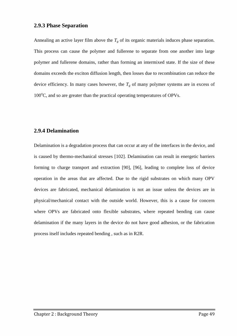
Chapter 2 : Background Theory Page 49
2.9.3 Phase Separation
Annealing an active layer film above the Tg of its organic materials induces phase separation.
This process can cause the polymer and fullerene to separate from one another into large
polymer and fullerene domains, rather than forming an intermixed state. If the size of these
domains exceeds the exciton diffusion length, then losses due to recombination can reduce the
device efficiency. In many cases however, the Tg of many polymer systems are in excess of
100oC, and so are greater than the practical operating temperatures of OPVs.
2.9.4 Delamination
Delamination is a degradation process that can occur at any of the interfaces in the device, and
is caused by thermo-mechanical stresses [102]. Delamination can result in energetic barriers
forming to charge transport and extraction [90], [96], leading to complete loss of device
operation in the areas that are affected. Due to the rigid substrates on which many OPV
devices are fabricated, mechanical delamination is not an issue unless the devices are in
physical/mechanical contact with the outside world. However, this is a cause for concern
where OPVs are fabricated onto flexible substrates, where repeated bending can cause
delamination if the many layers in the device do not have good adhesion, or the fabrication
process itself includes repeated bending , such as in R2R.
Chapter 2 : Background Theory Page 50
2.9.5 Encapsulation
The lifetime of OPVs can be significantly improved by encapsulating the device, whilst also
improving the mechanical stability and scratch resistance. Encapsulation protects the OPV
from oxygen and moisture (two major degradation sources), and also from UV radiation.
Ideally, encapsulation would seal the OPV in a glass container with an inert atmosphere to
completely exclude oxygen and water as shown in Figure 2.22, but unfortunately this is not
practical in many cases.
Figure 2.22 A 10 cm2 OPV encapsulated in a glass ampoule sealed under high vacuum [103].
The electrical connections to the inside of the ampoule are made using tungsten glass seals.
The sealing procedure is laborious, but the container is impervious to both oxygen and water.
The white glued caps are protecting the glass seal and does not represent sealing itself. The
aluminium foil is a heat shield necessary for the sealing procedure.
The most common form of encapsulation involves encasing the device between two sheets of
glass, one being the device substrate, using a glue to seal the edges. Lifetimes of 5600 hours
have been reached for OLEDs using this technique [104], and requirements for oxygen and
moisture penetration rates are more stringent for OLEDs than OPVs [105]. Although using
glass substrates and encapsulation sacrifices flexibility in the devices, glass has an extremely
Chapter 2 : Background Theory Page 51
low transmission rate of oxygen and water, which cannot currently be matched by flexible
alternatives.
Flexible encapsulation methods are of use for R2R processing. Polyethylene terephthalate
(PET) was one of the first materials studied for flexible encapsulation, but the results were far
from promising as the encapsulation technique itself reduced device lifetime [106]. Later
studies using a R2R process also used PET substrates and encapsulated films with far more
success [85], with lifetimes measured in tens of hours in air and hundreds of hours in a dry
nitrogen atmosphere.
Cros et al. [105] measured the lifetimes of both standard and inverted architecture OPV
devices to calculate the barrier water vapour transmission rate (WVTR) requirements for long
device lifetimes. They discovered that for lifetimes of several years, the necessary WVTR of
the encapsulating material must be of the order of 10-3
gm-2
day-1
or lower. This is
considerably lower than the number often quoted for OLEDs of 10-6
gm-2
day-1
[96]. This has
been correlated by results showing that lifetimes of up to 13500 hours are achievable for
devices encapsulated with a triple layer of SiNx/parylene, which has a WVTR of 3x10⁻³
gm-
2day
-1 [107].
2.9.6 Decay Behaviour
The degradation of OPVs is influenced by all the mechanisms covered in this section to
different degrees, determined by material choices and processing conditions. Determining the
dominant sources of degradation, and minimizing or eliminating them is one of the main
goals of research into OPVs.
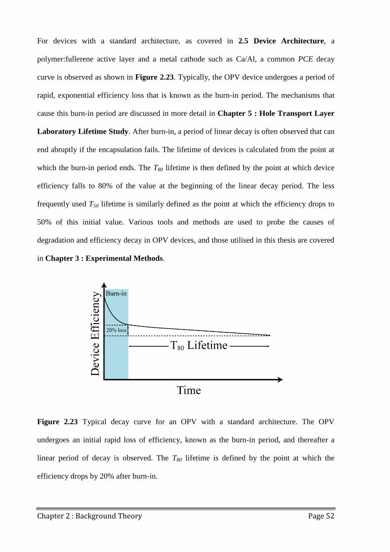
Chapter 2 : Background Theory Page 52
For devices with a standard architecture, as covered in 2.5 Device Architecture, a
polymer:fullerene active layer and a metal cathode such as Ca/Al, a common PCE decay
curve is observed as shown in Figure 2.23. Typically, the OPV device undergoes a period of
rapid, exponential efficiency loss that is known as the burn-in period. The mechanisms that
cause this burn-in period are discussed in more detail in Chapter 5 : Hole Transport Layer
Laboratory Lifetime Study. After burn-in, a period of linear decay is often observed that can
end abruptly if the encapsulation fails. The lifetime of devices is calculated from the point at
which the burn-in period ends. The T80 lifetime is then defined by the point at which device
efficiency falls to 80% of the value at the beginning of the linear decay period. The less
frequently used T50 lifetime is similarly defined as the point at which the efficiency drops to
50% of this initial value. Various tools and methods are used to probe the causes of
degradation and efficiency decay in OPV devices, and those utilised in this thesis are covered
in Chapter 3 : Experimental Methods.
Figure 2.23 Typical decay curve for an OPV with a standard architecture. The OPV
undergoes an initial rapid loss of efficiency, known as the burn-in period, and thereafter a
linear period of decay is observed. The T80 lifetime is defined by the point at which the
efficiency drops by 20% after burn-in.

Chapter 2 : Background Theory Page 53
2.10 References
[1] W. Heisenberg, “Uber den anschaulichen Inhalt der quantentheoretischen Kinematik
und Mechanik,” Zeitschrift fur Phys., vol. 43, no. 3–4, pp. 172–198, Mar. 1927.
[2] R. M. Eisberg and R. Resnick, Quantum physics of atoms, molecules, solids, nuclei,
and particles. New York: Wiley, 1974.
[3] S. W. Jonathan Clayden, Nick Greeves, Organic Chemistry, 2nd ed. Oxford: Oxford
University Press, 2012.
[4] N. Tessler, Y. Preezant, N. Rappaport, and Y. Roichman, “Charge Transport in
Disordered Organic Materials and Its Relevance to Thin-Film Devices: A Tutorial Review,”
Adv. Mater., vol. 21, no. 27, pp. 2741–2761, Jul. 2009.
[5] W. R. Salaneck, R. H. Friend, and J. L. Brédas, “Electronic structure of conjugated
polymers: consequences of electron–lattice coupling,” Phys. Rep., vol. 319, no. 6, pp. 231–
251, Oct. 1999.
[6] C. H. Woo, P. M. Beaujuge, T. W. Holcombe, O. P. Lee, and J. M. J. Fréchet,
“Incorporation of furan into low band-gap polymers for efficient solar cells.,” J. Am. Chem.
Soc., vol. 132, no. 44, pp. 15547–9, Nov. 2010.
[7] A. Bhuwalka, J. F. Mike, M. He, J. J. Intemann, T. Nelson, M. D. Ewan, R. A.
Roggers, Z. Lin, and M. Jeffries-EL, “Quaterthiophene–Benzobisazole Copolymers for
Photovoltaic Cells: Effect of Heteroatom Placement and Substitution on the Optical and
Electronic Properties,” Macromolecules, vol. 44, no. 24, pp. 9611–9617, Dec. 2011.
Chapter 2 : Background Theory Page 54
[8] B. Kim, H. R. Yeom, M. H. Yun, J. Y. Kim, and C. Yang, “A Selenophene Analogue
of PCDTBT: Selective Fine-Tuning of LUMO to Lower of the Bandgap for Efficient Polymer
Solar Cells,” Macromolecules, vol. 45, no. 21, pp. 8658–8664, Nov. 2012.
[9] S. Das, P. B. Pati, and S. S. Zade, “Cyclopenta[ c ]thiophene-Based D–A Conjugated
Copolymers: Effect of Heteroatoms (S, Se, and N) of Benzazole Acceptors on the Properties
of Polymers,” Macromolecules, vol. 45, no. 13, pp. 5410–5417, Jul. 2012.
[10] S. Beaupré, A. Pron, S. H. Drouin, A. Najari, L. G. Mercier, A. Robitaille, and M.
Leclerc, “Thieno-, Furo-, and Selenopheno[3,4-c]pyrrole-4,6-dione Copolymers: Effect of the
Heteroatom on the Electrooptical Properties,” Macromolecules, vol. 45, no. 17, pp. 6906–
6914, Aug. 2012.
[11] T. M. Clarke and J. R. Durrant, “Charge photogeneration in organic solar cells.,”
Chem. Rev., vol. 110, no. 11, pp. 6736–67, Nov. 2010.
[12] J.-W. van der Horst, P. Bobbert, P. de Jong, M. Michels, G. Brocks, and P. Kelly, “Ab
initio prediction of the electronic and optical excitations in polythiophene: Isolated chains
versus bulk polymer,” Phys. Rev. B, vol. 61, no. 23, pp. 15817–15826, Jun. 2000.
[13] J.-L. Brédas, D. Beljonne, V. Coropceanu, and J. Cornil, “Charge-transfer and energy-
transfer processes in pi-conjugated oligomers and polymers: a molecular picture.,” Chem.
Rev., vol. 104, no. 11, pp. 4971–5004, Nov. 2004.
[14] B. C. Thompson and J. M. J. Fréchet, “Polymer-fullerene composite solar cells.,”
Angew. Chem. Int. Ed. Engl., vol. 47, no. 1, pp. 58–77, Jan. 2008.

Chapter 2 : Background Theory Page 55
[15] M. C. Scharber, D. Mühlbacher, M. Koppe, P. Denk, C. Waldauf, A. J. Heeger, and C.
J. Brabec, “Design Rules for Donors in Bulk-Heterojunction Solar Cells—Towards 10 %
Energy-Conversion Efficiency,” Adv. Mater., vol. 18, no. 6, pp. 789–794, Mar. 2006.
[16] H. Bässler, “Charge Transport in Disordered Organic Photoconductors a Monte Carlo
Simulation Study,” Phys. status solidi, vol. 175, no. 1, pp. 15–56, Jan. 1993.
[17] R. J. Kline, M. D. McGehee, E. N. Kadnikova, J. Liu, and J. M. J. Fréchet,
“Controlling the Field-Effect Mobility of Regioregular Polythiophene by Changing the
Molecular Weight,” Adv. Mater., vol. 15, no. 18, pp. 1519–1522, Sep. 2003.
[18] H. Yan, Z. Chen, Y. Zheng, C. Newman, J. R. Quinn, F. Dötz, M. Kastler, and A.
Facchetti, “A high-mobility electron-transporting polymer for printed transistors.,” Nature,
vol. 457, no. 7230, pp. 679–86, Feb. 2009.
[19] W. Ma, C. Yang, X. Gong, K. Lee, and A. J. Heeger, “Thermally Stable, Efficient
Polymer Solar Cells with Nanoscale Control of the Interpenetrating Network Morphology,”
Adv. Funct. Mater., vol. 15, no. 10, pp. 1617–1622, Oct. 2005.
[20] J. W. M. N. Rudden, Elements of Solid State Physics, 2nd Editio. Chicester: John
Wiley & Sons, 1993.
[21] S. Braun, W. R. Salaneck, and M. Fahlman, “Energy-Level Alignment at
Organic/Metal and Organic/Organic Interfaces,” Adv. Mater., vol. 21, no. 14–15, pp. 1450–
1472, Apr. 2009.

Chapter 2 : Background Theory Page 56
[22] V. D. Mihailetchi, P. W. M. Blom, J. C. Hummelen, and M. T. Rispens, “Cathode
dependence of the open-circuit voltage of polymer:fullerene bulk heterojunction solar cells,”
J. Appl. Phys., vol. 94, no. 10, p. 6849, 2003.
[23] D. Rauh, A. Wagenpfahl, C. Deibel, and V. Dyakonov, “Relation of open circuit
voltage to charge carrier density in organic bulk heterojunction solar cells,” Appl. Phys. Lett.,
vol. 98, no. 13, p. 133301, 2011.
[24] Z. He, C. Zhong, X. Huang, W.-Y. Wong, H. Wu, L. Chen, S. Su, and Y. Cao,
“Simultaneous enhancement of open-circuit voltage, short-circuit current density, and fill
factor in polymer solar cells.,” Adv. Mater., vol. 23, no. 40, pp. 4636–43, Oct. 2011.
[25] S. H. Park, A. Roy, S. Beaupré, S. Cho, N. Coates, J. S. Moon, D. Moses, M. Leclerc,
K. Lee, and A. J. Heeger, “Bulk heterojunction solar cells with internal quantum efficiency
approaching 100%,” Nat. Photonics, vol. 3, no. 5, pp. 297–302, Apr. 2009.
[26] B. Rand, D. Burk, and S. Forrest, “Offset energies at organic semiconductor
heterojunctions and their influence on the open-circuit voltage of thin-film solar cells,” Phys.
Rev. B, vol. 75, no. 11, p. 115327, Mar. 2007.
[27] A. Maurano, R. Hamilton, C. G. Shuttle, A. M. Ballantyne, J. Nelson, B. O’Regan, W.
Zhang, I. McCulloch, H. Azimi, M. Morana, C. J. Brabec, and J. R. Durrant, “Recombination
dynamics as a key determinant of open circuit voltage in organic bulk heterojunction solar
cells: A comparison of four different donor polymers,” Adv. Mater., vol. 22, no. 44, pp. 4987–
4992, Nov. 2010.
[28] P. Schilinsky, “Simulation of light intensity dependent current characteristics of
polymer solar cells,” J. Appl. Phys., vol. 95, no. 5, p. 2816, 2004.
Chapter 2 : Background Theory Page 57
[29] L. J. A. Koster, V. D. Mihailetchi, R. Ramaker, and P. W. M. Blom, “Light intensity
dependence of open-circuit voltage of polymer:fullerene solar cells,” Appl. Phys. Lett., vol.
86, no. 12, p. 123509, 2005.
[30] K. Vandewal, K. Tvingstedt, A. Gadisa, O. Inganäs, and J. V Manca, “On the origin of
the open-circuit voltage of polymer-fullerene solar cells.,” Nat. Mater., vol. 8, no. 11, pp.
904–9, Nov. 2009.
[31] J. Liu, Y. Shi, and Y. Yang, “Solvation-Induced Morphology Effects on the
Performance of Polymer-Based Photovoltaic Devices,” Adv. Funct. Mater., vol. 11, no. 6, p.
420, Dec. 2001.
[32] H. Hoppe, M. Niggemann, C. Winder, J. Kraut, R. Hiesgen, a. Hinsch, D. Meissner,
and N. S. Sariciftci, “Nanoscale Morphology of Conjugated Polymer/Fullerene-Based Bulk-
Heterojunction Solar Cells,” Adv. Funct. Mater., vol. 14, no. 10, pp. 1005–1011, Oct. 2004.
[33] A. K. Ghosh, “Rectification, space-charge-limited current, photovoltaic and
photoconductive properties of Al∕tetracene∕Au sandwich cell,” J. Appl. Phys., vol. 44, no. 6, p.
2781, 1973.
[34] A. K. Ghosh and T. Feng, “Merocynanine organic solar cells,” J. Appl. Phys., vol. 49,
no. 12, p. 5982, 1978.
[35] C. W. Tang, “Two-layer organic photovoltaic cell,” Appl. Phys. Lett., vol. 48, no. 2, p.
183, 1986.
Chapter 2 : Background Theory Page 58
[36] J. J. M. Halls, C. A. Walsh, N. C. Greenham, E. A. Marseglia, R. H. Friend, S. C.
Moratti, and A. B. Holmes, “Efficient photodiodes from interpenetrating polymer networks,”
Nature, vol. 376, no. 6540, pp. 498–500, Aug. 1995.
[37] G. Yu, J. Gao, J. C. Hummelen, F. Wudl, and A. J. Heeger, “Polymer Photovoltaic
Cells: Enhanced Efficiencies via a Network of Internal Donor-Acceptor Heterojunctions,”
Science (80-. )., vol. 270, no. 5243, pp. 1789–1791, Dec. 1995.
[38] C. J. Brabec, M. Heeney, I. McCulloch, and J. Nelson, “Influence of blend
microstructure on bulk heterojunction organic photovoltaic performance.,” Chem. Soc. Rev.,
vol. 40, no. 3, pp. 1185–1199, Mar. 2011.
[39] J. Jung, D. Kim, W. S. Shin, S.-J. Moon, C. Lee, and S. C. Yoon, “Highly Efficient
Organic Photovoltaic Cells with Molybdenum Oxide Buffer Layer,” Jpn. J. Appl. Phys., vol.
49, no. 5, p. 05EB05, May 2010.
[40] Y.-I. Lee, J.-H. Youn, M.-S. Ryu, J. Kim, H.-T. Moon, and J. Jang, “Highly stable
inverted poly (3-hexylthiophene):methano-fullerene [6,6]-phenyl C71-butyric acid methyl
ester bulk heterojunction solar cell with thin oxide nano particle layer using solution process,”
Curr. Appl. Phys., vol. 12, pp. e46–e48, Sep. 2012.
[41] B. Zimmermann, U. Würfel, and M. Niggemann, “Longterm stability of efficient
inverted P3HT:PCBM solar cells,” Sol. Energy Mater. Sol. Cells, vol. 93, no. 4, pp. 491–496,
Apr. 2009.
[42] A. M. Nardes, M. Kemerink, M. M. de Kok, E. Vinken, K. Maturova, and R. A. J.
Janssen, “Conductivity, work function, and environmental stability of PEDOT:PSS thin films
treated with sorbitol,” Org. Electron., vol. 9, no. 5, pp. 727–734, Oct. 2008.
Chapter 2 : Background Theory Page 59
[43] Q. Wei, M. Mukaida, Y. Naitoh, and T. Ishida, “Morphological change and mobility
enhancement in PEDOT:PSS by adding co-solvents.,” Adv. Mater., vol. 25, no. 20, pp. 2831–
6, May 2013.
[44] J. Huang, P. F. Miller, J. S. Wilson, A. J. de Mello, J. C. de Mello, and D. D. C.
Bradley, “Investigation of the Effects of Doping and Post-Deposition Treatments on the
Conductivity, Morphology, and Work Function of Poly(3,4-
ethylenedioxythiophene)/Poly(styrene sulfonate) Films,” Adv. Funct. Mater., vol. 15, no. 2,
pp. 290–296, Feb. 2005.
[45] C. Jonda, A. B. R. Mayer, U. Stolz, A. Elschner, and A. Karbach, “Surface roughness
effects and their influence on the degradation of organic light emitting devices,” J. Mater.
Sci., vol. 35, no. 22, pp. 5645–5651, 2000.
[46] S. Tokito, K. Noda, and Y. Taga, “Metal oxides as a hole-injecting layer for an
organic electroluminescent device,” J. Phys. D. Appl. Phys., vol. 29, no. 11, pp. 2750–2753,
Nov. 1996.
[47] K. J. Reynolds, J. A. Barker, N. C. Greenham, R. H. Friend, and G. L. Frey,
“Inorganic solution-processed hole-injecting and electron-blocking layers in polymer light-
emitting diodes,” J. Appl. Phys., vol. 92, no. 12, p. 7556, 2002.
[48] F. Liu, S. Shao, X. Guo, Y. Zhao, and Z. Xie, “Efficient polymer photovoltaic cells
using solution-processed MoO3 as anode buffer layer,” Sol. Energy Mater. Sol. Cells, vol. 94,
no. 5, pp. 842–845, May 2010.
Chapter 2 : Background Theory Page 60
[49] J. Kettle, H. Waters, M. Horie, and S.-W. Chang, “Effect of hole transporting layers
on the performance of PCPDTBT : PCBM organic solar cells,” J. Phys. D. Appl. Phys., vol.
45, no. 12, p. 125102, Mar. 2012.
[50] Y. Sun, J. H. Seo, C. J. Takacs, J. Seifter, and A. J. Heeger, “Inverted polymer solar
cells integrated with a low-temperature-annealed sol-gel-derived ZnO film as an electron
transport layer,” Adv. Mater., vol. 23, no. 14, pp. 1679–1683, Apr. 2011.
[51] J. Kim, G. Kim, Y. Choi, J. Lee, S. Heum Park, and K. Lee, “Light-soaking issue in
polymer solar cells: Photoinduced energy level alignment at the sol-gel processed metal oxide
and indium tin oxide interface,” J. Appl. Phys., vol. 111, no. 11, p. 114511, 2012.
[52] T. Gershon, “Metal oxide applications in organic-based photovoltaics,” Mater. Sci.
Technol., vol. 27, no. 9, pp. 1357–1371, Sep. 2011.
[53] J. Meyer, S. Hamwi, M. Kröger, W. Kowalsky, T. Riedl, and A. Kahn, “Transition
metal oxides for organic electronics: energetics, device physics and applications.,” Adv.
Mater., vol. 24, no. 40, pp. 5408–27, Oct. 2012.
[54] G. Chamberlain, “Organic solar cells: A review,” Sol. Cells, vol. 8, no. 1, pp. 47–83,
1983.
[55] A. J. Campbell, D. D. C. Bradley, and D. G. Lidzey, “Space-charge limited
conduction with traps in poly(phenylene vinylene) light emitting diodes,” J. Appl. Phys., vol.
82, no. 12, p. 6326, 1997.
Chapter 2 : Background Theory Page 61
[56] S. E. Shaheen, C. J. Brabec, S. N. Sariciftci, F. Padinger, T. Fromherz, and J. C.
Hummelen, “2.5% Efficient Organic Plastic Solar Cells,” Appl. Phys. Lett., vol. 78, no. 6, pp.
841–843, 2001.
[57] F. Padinger, R. S. Rittberger, and N. S. Sariciftci, “Effects of Postproduction
Treatment on Plastic Solar Cells,” Adv. Funct. Mater., vol. 13, no. 1, pp. 85–88, 2003.
[58] Y. Kim, S. Cook, S. M. Tuladhar, S. A. Choulis, J. Nelson, J. R. Durrant, D. D. C.
Bradley, M. Giles, I. McCulloch, C.-S. Ha, and M. Ree, “A strong regioregularity effect in
self-organizing conjugated polymer films and high-efficiency polythiophene:fullerene solar
cells,” Nature Materials, vol. 5, no. 3. pp. 197–203, 05-Feb-2006.
[59] M. D. Irwin, D. B. Buchholz, A. W. Hains, R. P. H. Chang, and T. J. Marks, “p-Type
semiconducting nickel oxide as an efficiency-enhancing anode interfacial layer in polymer
bulk-heterojunction solar cells,” Proc. Natl. Acad. Sci., pp. 2–6, 2007.
[60] A. J. Moulé and K. Meerholz, “Controlling Morphology in Polymer–Fullerene
Mixtures,” Adv. Mater., vol. 20, no. 2, pp. 240–245, Jan. 2008.
[61] S. Cho, J. H. Seo, S. H. Park, S. Beaupré, M. Leclerc, and A. J. Heeger, “A thermally
stable semiconducting polymer.,” Adv. Mater., vol. 22, no. 11, pp. 1253–7, Mar. 2010.
[62] Y. Liang, Z. Xu, J. Xia, S.-T. Tsai, Y. Wu, G. Li, C. Ray, and L. Yu, “For the bright
future-bulk heterojunction polymer solar cells with power conversion efficiency of 7.4%.,”
Adv. Mater., vol. 22, no. 20, pp. E135–8, May 2010.
Chapter 2 : Background Theory Page 62
[63] Y. Sun, C. J. Takacs, S. R. Cowan, J. H. Seo, X. Gong, A. Roy, and A. J. Heeger,
“Efficient, air-stable bulk heterojunction polymer solar cells using MoO x as the anode
interfacial layer,” Adv. Mater., vol. 23, no. 19, pp. 2226–2230, May 2011.
[64] D. C. Watters, J. Kingsley, H. Yi, T. Wang, A. Iraqi, and D. Lidzey, “Optimising the
efficiency of carbazole co-polymer solar-cells by control over the metal cathode electrode,”
Org. Electron., vol. 13, no. 8, pp. 1401–1408, Aug. 2012.
[65] T. Wang, A. J. Pearson, A. D. F. Dunbar, P. A. Staniec, D. C. Watters, H. Yi, A. J.
Ryan, R. A. L. Jones, A. Iraqi, and D. G. Lidzey, “Correlating Structure with Function in
Thermally Annealed PCDTBT:PC70BM Photovoltaic Blends,” Adv. Funct. Mater., vol. 22,
no. 7, pp. 1399–1408, Apr. 2012.
[66] J. Liu, S. Shao, G. Fang, B. Meng, Z. Xie, and L. Wang, “High-efficiency inverted
polymer solar cells with transparent and work-function tunable MoO(3)-Al composite film as
cathode buffer layer.,” Adv. Mater., vol. 24, no. 20, pp. 2774–9, May 2012.
[67] C. H. Peters, I. T. Sachs-Quintana, W. R. Mateker, T. Heumueller, J. Rivnay, R.
Noriega, Z. M. Beiley, E. T. Hoke, A. Salleo, and M. D. McGehee, “The mechanism of burn-
in loss in a high efficiency polymer solar cell,” Adv. Mater., vol. 24, no. 5, pp. 663–668, Feb.
2012.
[68] C. H. Peters, I. T. Sachs-Quintana, J. P. Kastrop, S. Beaupré, M. Leclerc, and M. D.
McGehee, “High Efficiency Polymer Solar Cells with Long Operating Lifetimes,” Adv.
Energy Mater., vol. 1, no. 4, pp. 491–494, Jul. 2011.
Chapter 2 : Background Theory Page 63
[69] H. Yi, S. Al-Faifi, A. Iraqi, D. C. Watters, J. Kingsley, and D. G. Lidzey, “Carbazole
and thienyl benzo[1,2,5]thiadiazole based polymers with improved open circuit voltages and
processability for application in solar cells,” J. Mater. Chem., vol. 21, no. 35, p. 13649, 2011.
[70] D. C. Watters, H. Yi, A. J. Pearson, J. Kingsley, A. Iraqi, and D. Lidzey, “Fluorene-
based co-polymer with high hole mobility and device performance in bulk heterojunction
organic solar cells.,” Macromol. Rapid Commun., vol. 34, no. 14, pp. 1157–62, Jul. 2013.
[71] Z. Chen, H. Lemke, S. Albert-Seifried, M. Caironi, M. M. Nielsen, M. Heeney, W.
Zhang, I. McCulloch, and H. Sirringhaus, “High mobility ambipolar charge transport in
polyselenophene conjugated polymers.,” Adv. Mater., vol. 22, no. 21, pp. 2371–5, Jun. 2010.
[72] Q. Hou, Y. Xu, W. Yang, M. Yuan, J. Peng, and Y. Cao, “Novel red-emitting
fluorene-based copolymers,” J. Mater. Chem., vol. 12, no. 10, pp. 2887–2892, Sep. 2002.
[73] M. Bernius, M. Inbasekaran, E. Woo, W. Wu, and L. Wujkowski, “Fluorene-based
polymers-preparation and applications,” J. Mater. Sci. Mater. Electron., vol. 11, no. 2, pp.
111–116, 2000.
[74] G. Klärner, J.-I. Lee, M. H. Davey, and R. D. Miller, “Exciton Migration and
Trapping in Copolymers Based on Dialkylfluorenes,” Adv. Mater., vol. 11, no. 2, pp. 115–
119, Feb. 1999.
[75] W.-Y. Wong, “Metallated molecular materials of fluorene derivatives and their
analogues,” Coord. Chem. Rev., vol. 249, no. 9–10, pp. 971–997, May 2005.
Chapter 2 : Background Theory Page 64
[76] Z. He, C. Zhong, S. Su, M. Xu, H. Wu, and Y. Cao, “Enhanced power-conversion
efficiency in polymer solar cells using an inverted device structure,” Nat. Photonics, vol. 6,
no. 9, pp. 593–597, Aug. 2012.
[77] H. W. Kroto, J. R. Heath, S. C. O’Brien, R. F. Curl, and R. E. Smalley, “C60:
Buckminsterfullerene,” Nature, vol. 318, no. 6042, pp. 162–163, Nov. 1985.
[78] N. S. Sariciftci, L. Smilowitz, A. J. Heeger, and F. Wudl, “Photoinduced Electron
Transfer from a Conducting Polymer to Buckminsterfullerene,” Sci. , vol. 258 , no. 5087 , pp.
1474–1476, Nov. 1992.
[79] T. B. Singh, N. Marjanović, G. J. Matt, S. Günes, N. S. Sariciftci, A. Montaigne
Ramil, A. Andreev, H. Sitter, R. Schwödiauer, and S. Bauer, “High-mobility n-channel
organic field-effect transistors based on epitaxially grown C60 films,” Org. Electron., vol. 6,
no. 3, pp. 105–110, Jun. 2005.
[80] J. W. Arbogast and C. S. Foote, “Photophysical properties of C70,” J. Am. Chem.
Soc., vol. 113, no. 23, pp. 8886–8889, 1991.
[81] A. Seemann, H.-J. Egelhaaf, C. J. Brabec, and J. A. Hauch, “Influence of oxygen on
semi-transparent organic solar cells with gas permeable electrodes,” Org. Electron., vol. 10,
no. 8, pp. 1424–1428, Dec. 2009.
[82] V. Chellappan, G. M. Ng, M. J. Tan, W.-P. Goh, and F. Zhu, “Imbalanced charge
mobility in oxygen treated polythiophene/fullerene based bulk heterojunction solar cells,”
Appl. Phys. Lett., vol. 95, no. 26, p. 263305, 2009.
Chapter 2 : Background Theory Page 65
[83] C.-Y. Nam, D. Su, and C. T. Black, “High-Performance Air-Processed Polymer-
Fullerene Bulk Heterojunction Solar Cells,” Adv. Funct. Mater., vol. 19, no. 22, pp. 3552–
3559, Nov. 2009.
[84] J.-W. Kang, Y.-J. Kang, S. Jung, M. Song, D.-G. Kim, C. Su Kim, and S. H. Kim,
“Fully spray-coated inverted organic solar cells,” Sol. Energy Mater. Sol. Cells, vol. 103, pp.
76–79, Aug. 2012.
[85] F. C. Krebs, S. A. Gevorgyan, and J. Alstrup, “A roll-to-roll process to flexible
polymer solar cells: model studies, manufacture and operational stability studies,” J. Mater.
Chem., vol. 19, no. 30, p. 5442, 2009.
[86] S. Wu, J. Li, Q. Tai, and F. Yan, “Investigation of High-Performance Air-Processed
Poly(3-hexylthiophene)/Methanofullerene Bulk-Heterojunction Solar Cells,” Sol. Cells, vol.
114, no. 49, pp. 21873–21877, 2010.
[87] S. K. Hau, H.-L. Yip, H. Ma, and A. K.-Y. Jen, “High performance ambient processed
inverted polymer solar cells through interfacial modification with a fullerene self-assembled
monolayer,” Appl. Phys. Lett., vol. 93, no. 23, p. 233304, 2008.
[88] R. De Bettignies, J. Leroy, M. Firon, and C. Sentein, “Accelerated lifetime
measurements of P3HT:PCBM solar cells,” Synth. Met., vol. 156, no. 7–8, pp. 510–513, Apr.
2006.
[89] J. A. Hauch, P. Schilinsky, S. A. Choulis, R. Childers, M. Biele, and C. J. Brabec,
“Flexible organic P3HT:PCBM bulk-heterojunction modules with more than 1 year outdoor
lifetime,” Sol. Energy Mater. Sol. Cells, vol. 92, no. 7, pp. 727–731, Jul. 2008.
Chapter 2 : Background Theory Page 66
[90] M. O. Reese, A. J. Morfa, M. S. White, N. Kopidakis, S. E. Shaheen, G. Rumbles, and
D. S. Ginley, “Pathways for the degradation of organic photovoltaic P3HT:PCBM based
devices,” Sol. Energy Mater. Sol. Cells, vol. 92, no. 7, pp. 746–752, Jul. 2008.
[91] S. A. Gevorgyan, M. V. Madsen, H. F. Dam, M. Jørgensen, C. J. Fell, K. F. Anderson,
B. C. Duck, A. Mescheloff, E. A. Katz, A. Elschner, R. Roesch, H. Hoppe, M. Hermenau, M.
Riede, and F. C. Krebs, “Interlaboratory outdoor stability studies of flexible roll-to-roll coated
organic photovoltaic modules: Stability over 10,000h,” Sol. Energy Mater. Sol. Cells, vol.
116, pp. 187–196, Sep. 2013.
[92] H. Cao, W. He, Y. Mao, X. Lin, K. Ishikawa, J. H. Dickerson, and W. P. Hess,
“Recent progress in degradation and stabilization of organic solar cells,” J. Power Sources,
vol. 264, pp. 168–183, Oct. 2014.
[93] M. O. Reese, S. A. Gevorgyan, M. Jørgensen, E. Bundgaard, S. R. Kurtz, D. S.
Ginley, D. C. Olson, M. T. Lloyd, P. Morvillo, E. A. Katz, A. Elschner, O. Haillant, T. R.
Currier, V. Shrotriya, M. Hermenau, M. Riede, K. R. Kirov, G. Trimmel, T. Rath, O. Inganäs,
F. Zhang, M. Andersson, K. Tvingstedt, M. Lira-Cantu, D. Laird, C. McGuiness, S. (Jimmy)
Gowrisanker, M. Pannone, M. Xiao, J. Hauch, R. Steim, D. M. DeLongchamp, R. Rösch, H.
Hoppe, N. Espinosa, A. Urbina, G. Yaman-Uzunoglu, J.-B. Bonekamp, A. J. J. M. van
Breemen, C. Girotto, E. Voroshazi, and F. C. Krebs, “Consensus stability testing protocols for
organic photovoltaic materials and devices,” Sol. Energy Mater. Sol. Cells, vol. 95, no. 5, pp.
1253–1267, May 2011.
[94] Q. Pei, G. Zuccarello, M. Ahlskog, and O. Inganäs, “Electrochromic and highly stable
poly(3,4-ethylenedioxythiophene) switches between opaque blue-black and transparent sky
blue,” Polymer (Guildf)., vol. 35, no. 7, pp. 1347–1351, Mar. 1994.
Chapter 2 : Background Theory Page 67
[95] L. S. Hung, C. W. Tang, and M. G. Mason, “Enhanced electron injection in organic
electroluminescence devices using an Al/LiF electrode,” Appl. Phys. Lett., vol. 70, no. 2, p.
152, 1997.
[96] M. Jørgensen, K. Norrman, S. A. Gevorgyan, T. Tromholt, B. Andreasen, and F. C.
Krebs, “Stability of polymer solar cells.,” Adv. Mater., vol. 24, no. 5, pp. 580–612, Feb. 2012.
[97] L.-M. Chen, Z. Xu, Z. Hong, and Y. Yang, “Interface investigation and engineering –
achieving high performance polymer photovoltaic devices,” J. Mater. Chem., vol. 20, no. 13,
p. 2575, 2010.
[98] E. Voroshazi, B. Verreet, A. Buri, R. Müller, D. Di Nuzzo, and P. Heremans,
“Influence of cathode oxidation via the hole extraction layer in polymer:fullerene solar cells,”
Org. Electron., vol. 12, no. 5, pp. 736–744, May 2011.
[99] C. Girotto, E. Voroshazi, D. Cheyns, P. Heremans, and B. P. Rand, “Solution-
processed MoO₃ thin films as a hole-injection layer for organic solar cells.,” ACS Appl.
Mater. interfaces, vol. 3, no. 9, pp. 3244–7, 2011.
[100] M. Elshobaki, J. Anderegg, and S. Chaudhary, “Efficient polymer solar cells
fabricated on poly(3,4-ethylenedioxythiophene):poly(styrenesulfonate)-etched old indium tin
oxide substrates.,” ACS Appl. Mater. Interfaces, vol. 6, no. 15, pp. 12196–202, Aug. 2014.
[101] M. T. Lloyd, D. C. Olson, P. Lu, E. Fang, D. L. Moore, M. S. White, M. O. Reese, D.
S. Ginley, and J. W. P. Hsu, “Impact of contact evolution on the shelf life of organic solar
cells,” J. Mater. Chem., vol. 19, no. 41, p. 7638, 2009.
Chapter 2 : Background Theory Page 68
[102] S. R. Dupont, M. Oliver, F. C. Krebs, and R. H. Dauskardt, “Interlayer adhesion in
roll-to-roll processed flexible inverted polymer solar cells,” Sol. Energy Mater. Sol. Cells, vol.
97, pp. 171–175, Feb. 2012.
[103] F. C. Krebs, “Encapsulation of polymer photovoltaic prototypes,” Sol. Energy Mater.
Sol. Cells, vol. 90, no. 20, pp. 3633–3643, Dec. 2006.
[104] A. Asadpoordarvish, A. Sandström, S. Tang, J. Granström, and L. Edman,
“Encapsulating light-emitting electrochemical cells for improved performance,” Appl. Phys.
Lett., vol. 100, no. 19, p. 193508, 2012.
[105] S. Cros, R. de Bettignies, S. Berson, S. Bailly, P. Maisse, N. Lemaitre, and S.
Guillerez, “Definition of encapsulation barrier requirements: A method applied to organic
solar cells,” Sol. Energy Mater. Sol. Cells, vol. 95, pp. S65–S69, May 2011.
[106] F. C. Krebs, J. Alstrup, H. Spanggaard, K. Larsen, and E. Kold, “Production of large-
area polymer solar cells by industrial silk screen printing, lifetime considerations and
lamination with polyethyleneterephthalate,” Sol. Energy Mater. Sol. Cells, vol. 83, no. 2–3,
pp. 293–300, Jun. 2004.
[107] N. Kim, W. J. Potscavage, A. Sundaramoothi, C. Henderson, B. Kippelen, and S.
Graham, “A correlation study between barrier film performance and shelf lifetime of
encapsulated organic solar cells,” Sol. Energy Mater. Sol. Cells, vol. 101, pp. 140–146, Jun.
2012.

Chapter 3 : Experimental Methods Page 69
Chapter 3 : Experimental Methods
3.0 Introduction
In this chapter, the various techniques utilised in the fabrication of OPV devices are reported,
as are the experimental techniques employed to characterise devices and determine a variety
of operating parameters. Key fabrication techniques covered include substrate cleaning,
solution preparation, thin film deposition, metal evaporation and encapsulation. Experimental
techniques used to probe OPV device performance include current-density (JV)
characterisation, laser beam induced current mapping (LBIC), electroluminescent mapping
(ELM), absorbance spectroscopy, external quantum efficiency (EQE) and spectroscopic
ellipsometry. Finally, the details of lifetime testing protocols and apparatus are covered,
including set up and calibration.
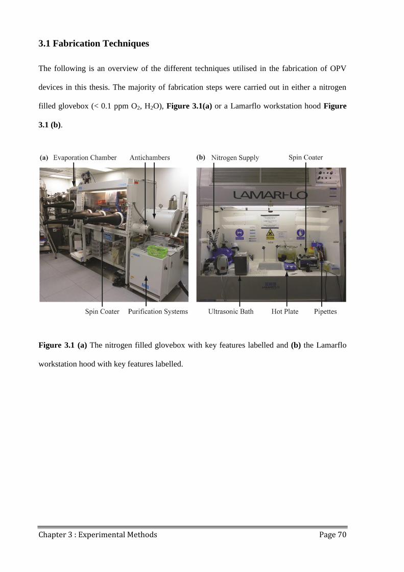
Chapter 3 : Experimental Methods Page 70
3.1 Fabrication Techniques
The following is an overview of the different techniques utilised in the fabrication of OPV
devices in this thesis. The majority of fabrication steps were carried out in either a nitrogen
filled glovebox (< 0.1 ppm O2, H2O), Figure 3.1(a) or a Lamarflo workstation hood Figure
3.1 (b).
Figure 3.1 (a) The nitrogen filled glovebox with key features labelled and (b) the Lamarflo
workstation hood with key features labelled.

Chapter 3 : Experimental Methods Page 71
3.1.1 Substrate Cleaning
OPV devices were fabricated onto 20 mm x 15 mm glass substrates with a 100 nm thick pre-
patterned sputtered ITO layer supplied by Ossila Ltd. The overlap of the ITO pattern and top
electrical contact defines six 2 mm x 2 mm (4 mm2) pixels on each substrate as shown in
Figure 3.2 (b).
Figure 3.2 (a) Six pixel substrate design. (b) Pixels defined by overlap of ITO and metal
electrode.
The substrates were rigorously cleaned to remove dust and dirt on the surface of the ITO,
which can lead to shorts and other defects forming during device fabrication. This was done
by sonicating the substrates in a hot water ultrasonic bath (70 - 80oC) with Hellmanex III
cleaning fluid for 10 minutes, after which they were 'dump-rinsed' twice in hot DI water.
Once rinsed the substrates were sonicated for a further 10 minutes in 2-propanol (IPA) in a
hot water ultrasonic bath, and dump-rinsed in hot DI water once more. The substrates were
then stored in DI water until needed, for no more than an hour, at which point they were
removed from the DI water and dried with a compressed nitrogen jet.
Chapter 3 : Experimental Methods Page 72
3.1.2 Solution Preparation
One of the main benefits of OPV technology is the ability to process materials from solution.
This allows for the use of many different thin film deposition techniques, such as spin-
coating, spray coating, ink-jet printing and R2R processing. As previously mentioned in 2.5
Device Architecture, for the active layer of OPVs utilizing a BHJ morphology, both the
donor polymer and fullerene acceptor are deposited from the same solution, which results in
the interpenetrating network of phase separated materials needed for exciton dissociation and
charge extraction. Solution composition can drastically affect the resulting material film, and
therefore solution preparation is a key step in the deposition of thin films with the desired
properties for OPV device operation.
All materials and solvents were used as received from the suppliers. Solvents, metal oxide
precursors and other materials, unless otherwise stated, were sourced from Sigma-Aldrich.
Donor polymers and PC70BM (95% purity) were provided by either the University of
Sheffield (UoS) Chemistry Department or Ossila Ltd. Details of polymer source, molecular
weight (Mw) and number (Mn), polydispersity index (PDI) and optimum PC70BM blend ratio
can be found in Table 3.1.
Polymer solutions were prepared by dissolving dry polymer in a solvent, either chloroform
(CHCl3) or chlorobenzene (CB), at a concentration of 4 - 10 mgmL-1
depending on the
solubility of the polymer. Polymer solutions were then heated at 80oC for an hour with a
rotating stir bar, with periodic shaking of the vial to ensure all material was fully dissolved.
This solution was then cooled for 5 minutes before being added to another vial containing dry
PC70BM to attain the desired blend ratio. The polymer:fullerene solution was then heated
whilst stirring with a rotating stir bar for a further hour at 80oC, before being cooled down and
filtered through a polytetrafluoroethylene (PTFE) filter with a 0.45 µm pore size to remove
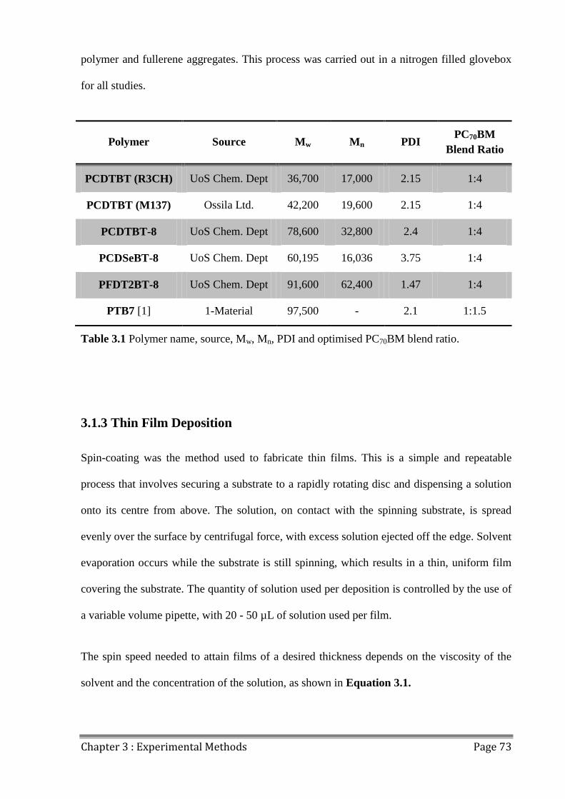
Chapter 3 : Experimental Methods Page 73
polymer and fullerene aggregates. This process was carried out in a nitrogen filled glovebox
for all studies.
Polymer Source Mw Mn PDI PC70BM
Blend Ratio
PCDTBT (R3CH) UoS Chem. Dept 36,700 17,000 2.15 1:4
PCDTBT (M137) Ossila Ltd. 42,200 19,600 2.15 1:4
PCDTBT-8 UoS Chem. Dept 78,600 32,800 2.4 1:4
PCDSeBT-8 UoS Chem. Dept 60,195 16,036 3.75 1:4
PFDT2BT-8 UoS Chem. Dept 91,600 62,400 1.47 1:4
PTB7 [1] 1-Material 97,500 - 2.1 1:1.5
Table 3.1 Polymer name, source, Mw, Mn, PDI and optimised PC70BM blend ratio.
3.1.3 Thin Film Deposition
Spin-coating was the method used to fabricate thin films. This is a simple and repeatable
process that involves securing a substrate to a rapidly rotating disc and dispensing a solution
onto its centre from above. The solution, on contact with the spinning substrate, is spread
evenly over the surface by centrifugal force, with excess solution ejected off the edge. Solvent
evaporation occurs while the substrate is still spinning, which results in a thin, uniform film
covering the substrate. The quantity of solution used per deposition is controlled by the use of
a variable volume pipette, with 20 - 50 µL of solution used per film.
The spin speed needed to attain films of a desired thickness depends on the viscosity of the
solvent and the concentration of the solution, as shown in Equation 3.1.
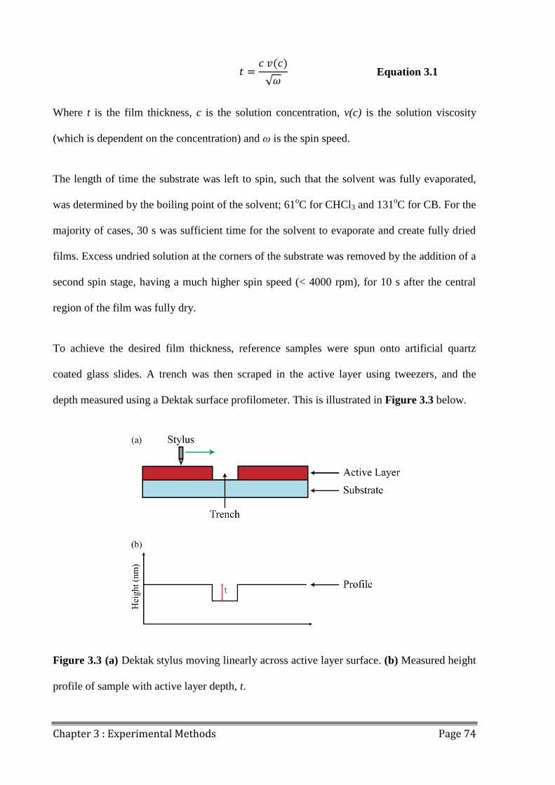
Chapter 3 : Experimental Methods Page 74
Equation 3.1
Where t is the film thickness, c is the solution concentration, v(c) is the solution viscosity
(which is dependent on the concentration) and ω is the spin speed.
The length of time the substrate was left to spin, such that the solvent was fully evaporated,
was determined by the boiling point of the solvent; 61oC for CHCl3 and 131
oC for CB. For the
majority of cases, 30 s was sufficient time for the solvent to evaporate and create fully dried
films. Excess undried solution at the corners of the substrate was removed by the addition of a
second spin stage, having a much higher spin speed (< 4000 rpm), for 10 s after the central
region of the film was fully dry.
To achieve the desired film thickness, reference samples were spun onto artificial quartz
coated glass slides. A trench was then scraped in the active layer using tweezers, and the
depth measured using a Dektak surface profilometer. This is illustrated in Figure 3.3 below.
Figure 3.3 (a) Dektak stylus moving linearly across active layer surface. (b) Measured height
profile of sample with active layer depth, t.

Chapter 3 : Experimental Methods Page 75
Once a reference sample had been measured, altering the spin speed of deposition allows for
fine-tuning of the film thickness, as governed by Equation 3.2.
Equation 3.2
Where tr is the film thickness of the reference sample created by spin speed ωr, and t2 is the
desired film thickness created by spin speed ω2. This relationship is dependent on the solution
concentration and viscosity being kept constant.
Active layer materials were spin-coated in the glovebox for the majority of the OPVs
fabricated, though in some cases deposition was carried out in air in a Lamarflo work bench.
PEDOT:PSS solutions (Heraeus Clevios™ P VP AI 4083) were filtered through a 0.45 µm
polyvinylidene fluoride (PVDF) filter to remove aggregates, and were spin-coated onto
cleaned ITO substrates at 6000 rpm for 30 s, to give a film thickness of 30 nm. PEDOT:PSS
solutions are aqueous, and therefore could not be processed in the glovebox, so thin films
were spin-coated in a Lamarflo work bench under ambient conditions. The films were then
thermally annealed in air at 150oC for 10 minutes prior to being transported to the glovebox,
where, in some cases, they were again annealed at 150oC for 10 minutes to remove any
remaining moisture in the films.
Other materials, such as metal oxides, were also deposited from solution. The solution
preparation details and deposition requirements for these materials are covered in the chapters
in which they are utilised.

Chapter 3 : Experimental Methods Page 76
3.1.4 Thermal Evaporation
Thermal evaporation is a technique by which metal oxide interlayers and metallic top contacts
can be deposited. Thermal evaporation involves two basic processes: a hot source material
evaporates, and then condenses on the substrate. This is carried out in a high vacuum, such
that the evaporated metal particles can travel directly to the substrate without colliding with
gas molecules. The high vacuum also reduces the boiling point of the materials being
evaporated, allowing for heating by electrical currents.
This process was carried out in a vacuum chamber attached to the nitrogen filled glovebox, as
shown in Figure 3.1 (a), to allow for substrates to be moved between the two without
exposure to ambient environment. The vacuum chamber had multiple sources, and so
sequential evaporations could be carried out without having to vent the chamber to
atmosphere. The thickness of the material being deposited were monitored during evaporation
using a calibrated quartz crystal microbalance (QCM), whose frequency changes depending
on the mass deposited on its surface.
For the deposition of evaporated materials, substrates were loaded into evaporation masks
which defined the area over which the material was evaporated onto the substrate, an example
of which is shown in Figure 3.4 (b).

Chapter 3 : Experimental Methods Page 77
Figure 3.4 (a) Design of the top contact evaporation mask for OPVs, with space for 35
substrates. The mask consists of two 2 mm thick layers of patterned stainless steel welded
together (represented by dark and light grey areas). (b) Shows a substrate loaded in the mask
(viewed from below, through the mask), and the exposed area of substrate onto which the
metal is evaporated. The pixel area is highlighted in red.
Once fully loaded with substrates, the mask was transferred to the evaporation chamber and
secured on a rotating holder to allow for uniform deposition across the surface. The chamber
was then pumped down to a starting pressure of < 10-7
mbar to allow for the metal to vaporise
and to remove trace gasses that could react with the materials being deposited. The chosen
materials were evaporated from crucibles by passing a current through a heating coil
surrounding the crucible. Depending on the material being evaporated, the optimum material
deposition rate, crucible material and final film thickness varied as shown in Table 3.2.
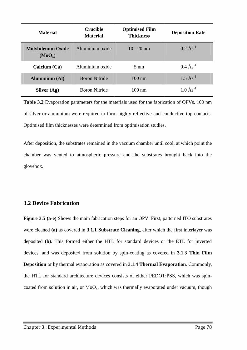
Chapter 3 : Experimental Methods Page 78
Material Crucible
Material
Optimised Film
Thickness Deposition Rate
Molybdenum Oxide
(MoOx)
Aluminium oxide 10 - 20 nm 0.2 Ås-1
Calcium (Ca) Aluminium oxide 5 nm 0.4 Ås-1
Aluminium (Al) Boron Nitride 100 nm 1.5 Ås-1
Silver (Ag) Boron Nitride 100 nm 1.0 Ås-1
Table 3.2 Evaporation parameters for the materials used for the fabrication of OPVs. 100 nm
of silver or aluminium were required to form highly reflective and conductive top contacts.
Optimised film thicknesses were determined from optimisation studies.
After deposition, the substrates remained in the vacuum chamber until cool, at which point the
chamber was vented to atmospheric pressure and the substrates brought back into the
glovebox.
3.2 Device Fabrication
Figure 3.5 (a-e) Shows the main fabrication steps for an OPV. First, patterned ITO substrates
were cleaned (a) as covered in 3.1.1 Substrate Cleaning, after which the first interlayer was
deposited (b). This formed either the HTL for standard devices or the ETL for inverted
devices, and was deposited from solution by spin-coating as covered in 3.1.3 Thin Film
Deposition or by thermal evaporation as covered in 3.1.4 Thermal Evaporation. Commonly,
the HTL for standard architecture devices consists of either PEDOT:PSS, which was spin-
coated from solution in air, or MoOx, which was thermally evaporated under vacuum, though
Chapter 3 : Experimental Methods Page 79
other materials were also used. The ITO contact points on either side of the substrate were
wiped clean of material to allow for efficient electrical contacts.
The active layer was then deposited by spin-coating (c), most often in the glovebox to prevent
degradation of the polymer films, though this process was also carried out in air in a Lamarflo
work bench in Chapter 4 : Air Stability of MoOx and Chapter 6 : Polymer Air
Processing. Optimum active layer thicknesses of between 70 - 95 nm were achieved by
varying the spin speed of deposition as covered in 3.1.3 Thin Film Deposition. As with the
first interlayer, the ITO contact points on either side of the substrate were cleaned of material
to allow for efficient electrical contacts.
Next, the second interlayer was deposited (d), forming the ETL for standard devices or the
HTL for inverted devices. This layer was formed of 5 nm of Ca or 10 nm of titanium oxide
(TiOx). Ca was thermally evaporated using an evaporation mask, and TiOx was processed
from solution as covered in 8.1 Titanium Oxide. For the TiOx, the ITO contact points on
either side of the substrate were cleaned of material as in previous steps.
100 nm of metal was deposited via thermal evaporation to form the top electrical contact (e)
in the vacuum chamber at < 10-7
mbar. This was carried out using an evaporation mask to
achieve the desired cathode shape and coverage as shown in Figure 3.4 (a).
Finally, devices were encapsulated using a glass cover slip and UV epoxy (f), which was
cured for 30 minutes under a UV lamp prior to removal from the glovebox. This
encapsulation provided protection from moisture and oxygen ingress into the device, and
mechanical stresses and scratches during handling. A completed device is shown in Figure
3.6.
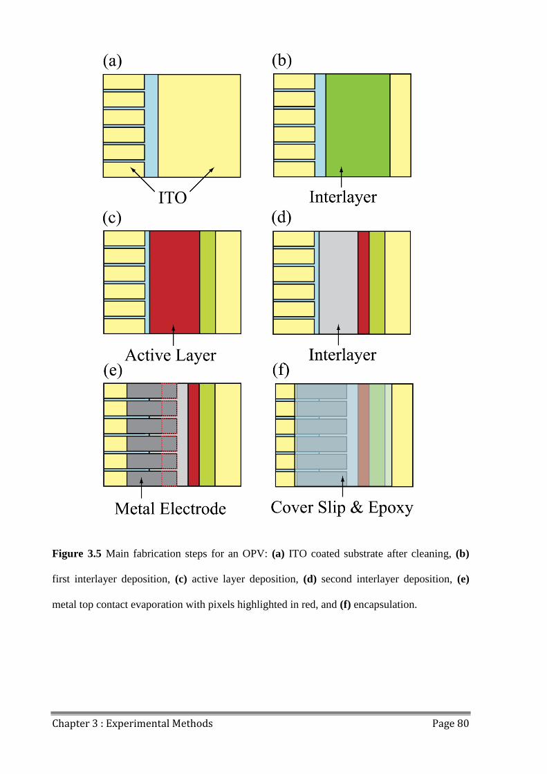
Chapter 3 : Experimental Methods Page 80
Figure 3.5 Main fabrication steps for an OPV: (a) ITO coated substrate after cleaning, (b)
first interlayer deposition, (c) active layer deposition, (d) second interlayer deposition, (e)
metal top contact evaporation with pixels highlighted in red, and (f) encapsulation.
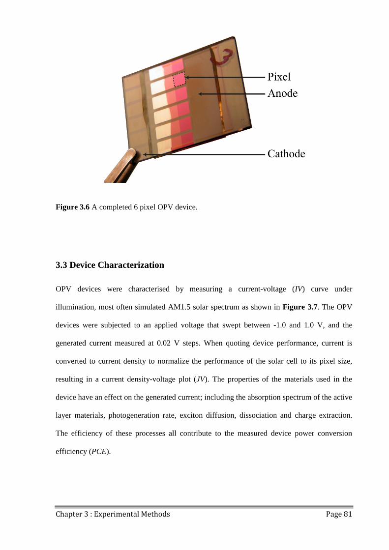
Chapter 3 : Experimental Methods Page 81
Figure 3.6 A completed 6 pixel OPV device.
3.3 Device Characterization
OPV devices were characterised by measuring a current-voltage (IV) curve under
illumination, most often simulated AM1.5 solar spectrum as shown in Figure 3.7. The OPV
devices were subjected to an applied voltage that swept between -1.0 and 1.0 V, and the
generated current measured at 0.02 V steps. When quoting device performance, current is
converted to current density to normalize the performance of the solar cell to its pixel size,
resulting in a current density-voltage plot (JV). The properties of the materials used in the
device have an effect on the generated current; including the absorption spectrum of the active
layer materials, photogeneration rate, exciton diffusion, dissociation and charge extraction.
The efficiency of these processes all contribute to the measured device power conversion
efficiency (PCE).

Chapter 3 : Experimental Methods Page 82
Figure 3.7 Solar spectrum incident on the Earth above the atmosphere (AM0) and on the
surface at temperate latitudes (AM1.5).
A typical example of a JV curve for an OPV device is shown in Figure 3.8, with the operating
parameters annotated. The device is at open circuit when J = 0 mAcm-2
and short-circuit at V
= 0 V. The PCE and the fill factor (FF) can be calculated using Equations 3.3 and 3.4 below.
Equation 3.3
Equation 3.4
Where Pin is the incident power from the simulated AM1.5 solar spectrum, Pout is the output
power of the device, Jmpp and Vmpp are the current density and voltage at the maximum power
point (Mpp), Voc is the open circuit voltage, Jsc is the short-circuit current density and FF is the
fill factor.
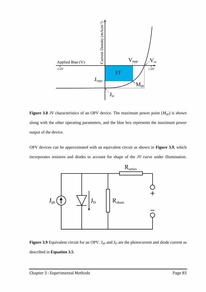
Chapter 3 : Experimental Methods Page 83
Figure 3.8 JV characteristics of an OPV device. The maximum power point (Mpp) is shown
along with the other operating parameters, and the blue box represents the maximum power
output of the device.
OPV devices can be approximated with an equivalent circuit as shown in Figure 3.9, which
incorporates resistors and diodes to account for shape of the JV curve under illumination.
Figure 3.9 Equivalent circuit for an OPV. Jph and JD are the photocurrent and diode current as
described in Equation 3.5.
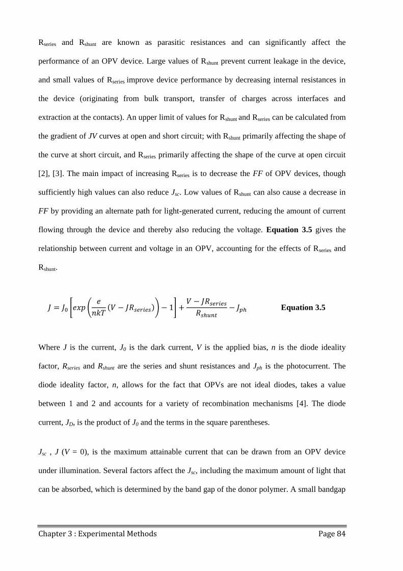
Chapter 3 : Experimental Methods Page 84
Rseries and Rshunt are known as parasitic resistances and can significantly affect the
performance of an OPV device. Large values of Rshunt prevent current leakage in the device,
and small values of Rseries improve device performance by decreasing internal resistances in
the device (originating from bulk transport, transfer of charges across interfaces and
extraction at the contacts). An upper limit of values for Rshunt and Rseries can be calculated from
the gradient of JV curves at open and short circuit; with Rshunt primarily affecting the shape of
the curve at short circuit, and Rseries primarily affecting the shape of the curve at open circuit
[2], [3]. The main impact of increasing Rseries is to decrease the FF of OPV devices, though
sufficiently high values can also reduce Jsc. Low values of Rshunt can also cause a decrease in
FF by providing an alternate path for light-generated current, reducing the amount of current
flowing through the device and thereby also reducing the voltage. Equation 3.5 gives the
relationship between current and voltage in an OPV, accounting for the effects of Rseries and
Rshunt.
Equation 3.5
Where J is the current, J0 is the dark current, V is the applied bias, n is the diode ideality
factor, Rseries and Rshunt are the series and shunt resistances and Jph is the photocurrent. The
diode ideality factor, n, allows for the fact that OPVs are not ideal diodes, takes a value
between 1 and 2 and accounts for a variety of recombination mechanisms [4]. The diode
current, JD, is the product of J0 and the terms in the square parentheses.
Jsc , J (V = 0), is the maximum attainable current that can be drawn from an OPV device
under illumination. Several factors affect the Jsc, including the maximum amount of light that
can be absorbed, which is determined by the band gap of the donor polymer. A small bandgap
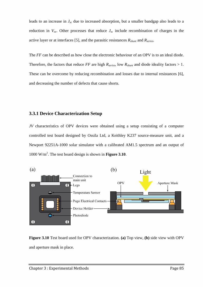
Chapter 3 : Experimental Methods Page 85
leads to an increase in Jsc due to increased absorption, but a smaller bandgap also leads to a
reduction in Voc. Other processes that reduce Jsc include recombination of charges in the
active layer or at interfaces [5], and the parasitic resistances Rshunt and Rseries.
The FF can be described as how close the electronic behaviour of an OPV is to an ideal diode.
Therefore, the factors that reduce FF are high Rseries, low Rshunt and diode ideality factors > 1.
These can be overcome by reducing recombination and losses due to internal resistances [6],
and decreasing the number of defects that cause shorts.
3.3.1 Device Characterization Setup
JV characteristics of OPV devices were obtained using a setup consisting of a computer
controlled test board designed by Ossila Ltd, a Keithley K237 source-measure unit, and a
Newport 92251A-1000 solar simulator with a calibrated AM1.5 spectrum and an output of
1000 W/m2. The test board design is shown in Figure 3.10.
Figure 3.10 Test board used for OPV characterization. (a) Top view, (b) side view with OPV
and aperture mask in place.
Chapter 3 : Experimental Methods Page 86
The test board was designed such that it would hold an OPV and an aperture mask on spring
loaded pogo electrical contacts, as shown in Figure 3.10 (b), uniformly illuminated from
above by the solar simulator. A temperature sensor and photodiode next to the OPV allowed
for monitoring of temperature and light intensity with every JV measurement. The test board
was secured underneath the solar simulator and connected to a main circuit board that allowed
for switching between the six pixels of the device for automated testing. The main circuit
board was connected to the Keithley 237 source-measure unit by BNC connection, and the
whole setup was controlled by a MATLAB program. This automated setup allowed for swift
and repeatable device testing. The calibration of the solar simulator and aperture masks are
covered in the following sections.
3.3.2 Solar Simulator Calibration
To check the calibration of the solar simulator at the University of Sheffield, the JV
characteristics of five OPVs were measured first at Sheffield and then later at Loughborough
University, whose solar simulator (CREST) had undergone rigorous calibration and testing to
accurately match the AM1.5 spectrum. The five OPV devices tested at both locations had an
ITO/MoOx/PCDTBT:PC70BM/Ca/Al standard architecture. Table 3.3 shows the average
values and standard deviation of PCE, FF, Voc and Jsc for the five different OPV devices,
omitting those pixels with gross film defects. The results were very similar, with a small
relative decrease of around 3-8% in PCE when the devices were measured in Loughborough.
The discrepancy in the two measurements could be accounted for by a spectral mismatch of
the two sources, degradation of the devices during transit and under repeated testing and other
differences in testing equipment.
Chapter 3 : Experimental Methods Page 87
Device Testing
Location PCE (%) FF Voc (V)
Jsc
(mAcm-2
)
1 Sheffield 4.93±0.04 65.4±0.3 0.87 -8.64±0.08
Loughborough 4.71±0.03 64.7±0.1 0.89 -8.15±0.04
2 Sheffield 4.95±0.04 65.7±0.3 0.87 -8.64±0.07
Loughborough 4.69±0.03 65.1±0.3 0.88 -8.18±0.08
3 Sheffield 5.14±0.04 66.2±0.1 0.88 -8.82±0.06
Loughborough 5.02±0.07 65.4±0.5 0.89 -8.6±0.2
4 Sheffield 5.01±0.04 65.5±0.3 0.88 -8.71±0.03
Loughborough 4.62±0.06 63.4±0.8 0.89 -8.19±0.01
5 Sheffield 5.18±0.02 66.1±0.2 0.88 -8.90±0.06
Loughborough 4.91±0.05 65.6±0.4 0.90 -8.32±0.07
Table 3.3 Operating parameters for five OPV devices tested at both Sheffield and
Loughborough Universities using different solar simulators.
The JV curves for pixel 3 of device 1 from Table 3.3, as measured under the Sheffield and
Loughborough solar simulators, are shown in Figure 3.11 for comparison.
Chapter 3 : Experimental Methods Page 88
Figure 3.11 JV curves for the same device measured using the Sheffield and Loughborough
solar simulators.
3.3.3 Aperture Mask Calibration
Devices were measured using a electrochemically etched aperture mask, the design of which
is shown in Figure 3.12 (a), to define an area of illumination and allow for accurate
calculation of current density. The masks were etched with individual apertures for each of
the six pixels, each with an area of 0.0256 cm2. However, the manufacturing process left a
roughened edge to these pixel apertures as can be seen in Figure 3.12 (b). Using an optical
microscope image of the pixel apertures and an eyepiece micrometer, shown in Figure 3.12
(b), (c) respectively, the area of the pixel apertures were calculated to be (0.0261±0.0001)cm2,
a 2% error from the value quoted by the manufacturers. This aperture calibration allowed for
more accurate calculation of the current density, and subsequently PCE.
Chapter 3 : Experimental Methods Page 89
Figure 3.12 (a) Design of the aperture mask for OPV characterization, (b) an optical
microscope image of an individual pixel aperture and (c) an optical microscope image of an
eyepiece micrometer.
3.4 Absorbance Spectroscopy
Absorbance spectroscopy was used to measure the transmission of light at different
wavelengths through a sample. This was carried out using a Jobin Yvon Horiba Fluoromax-4,
the structure of which is shown in Figure 3.13.
A Xenon arc lamp, with an emission starting at 250 nm, was used as the light source and was
housed in the first chamber of the Fluoromax. From the lamp, the light is focused using an
elliptical mirror, through a quartz window, and into a Czerny-Turner monochromator. The
light entering the monochromator is focused onto an entry slit, which is used to control the
intensity of the light. From here, the light is collimated using a mirror and is then incident
onto a blazed diffraction grating, where, upon diffraction, it is then refocused by a second
mirror onto another slit and exits the monochromator. This process allows for control of the
wavelength of light incident on the second slit, and is dependent on the angle of the blazed
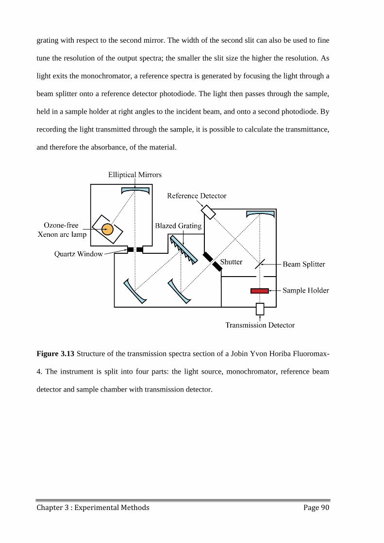
Chapter 3 : Experimental Methods Page 90
grating with respect to the second mirror. The width of the second slit can also be used to fine
tune the resolution of the output spectra; the smaller the slit size the higher the resolution. As
light exits the monochromator, a reference spectra is generated by focusing the light through a
beam splitter onto a reference detector photodiode. The light then passes through the sample,
held in a sample holder at right angles to the incident beam, and onto a second photodiode. By
recording the light transmitted through the sample, it is possible to calculate the transmittance,
and therefore the absorbance, of the material.
Figure 3.13 Structure of the transmission spectra section of a Jobin Yvon Horiba Fluoromax-
4. The instrument is split into four parts: the light source, monochromator, reference beam
detector and sample chamber with transmission detector.

Chapter 3 : Experimental Methods Page 91
The transmittance of a sample is calculated using the relationship shown in Equation 3.6.
Equation 3.6
where T(λ) is the fraction of light transmitted at wavelength λ, I(λ) is the amount of light
transmitted as measured by the sample photodiode, and I0(λ) is the amount of light incident on
the sample as measured by the reference photodiode. The transmittance, T(λ), includes losses
due to reflections and dispersion of light at interfaces. Therefore, for the measurement of thin
films deposited onto glass slides, transmission spectra of blank glass slides are taken to
determine the losses due to the substrate. Calculations assumptions include that the losses due
to the substrate are the same for both the reference blank glass slide and the sample to be
measured.
The absorption spectrum of a sample can be calculated from the transmission using Equation
3.7.
Equation 3.7
where A(λ) is the absorption at wavelength λ.
The transmittance of thin polymer films were measured from 350 - 900 nm in 2 nm steps with
a slit size of 2 nm.

Chapter 3 : Experimental Methods Page 92
3.5 Spectroscopic Ellipsometry
Spectroscopic ellipsometry is a technique that allows for the measurement of several
properties of thin films, including refractive index (n), extinction coefficient (k) and thickness.
This is done by measuring the change in the intensity and phase of polarised light as it is
reflected from the surface of a thin film of material on a silicon substrate. These changes
allow for the thickness, n and k to be modelled. A Woollam M-2000V ellipsometer was used,
with a wavelength range of 370 - 1000 nm.
The optical constants of the material are calculated by characterizing the amplitude of the
light parallel and perpendicular to the plane of incidence (Rp and Rs respectively). This gives
the reflectance ratio, ρ, as given in Equation 3.8.
Equation 3.8
where Ψ is the ratio of amplitudes and Δ the phase difference between the incident and
reflected light.
Using Ψ and Δ, it is possible to determine the material properties using an optical model that
approximates the structure of the material being measured. This technique was used in
Chapter 4 : Air Stability of MoOx to calculate the thickness changes of MoOx over time on
adsorption of water. Data was acquired by Dr. Tao Wang.
Chapter 3 : Experimental Methods Page 93
3.6 External Quantum Efficiency (EQE)
External Quantum Efficiency (EQE) is the ratio of the number of charge carriers collected at
the contacts of a solar cell per second to the number of incident photons of a given
wavelength shining on the solar cell per second as in Equation 3.9.
Equation 3.9
This gives information on the combined efficiency of several processes in the OPV, including
photon absorption, charge generation, separation and transport. An EQE of 100% means that
for a given wavelength, all incident photons are converted to free charges and collected at the
contacts. However, due to losses at many stages due to the aforementioned processes in 2.4
Photophysics of Organic Conjugated Polymers, OPV device EQE is < 100% for any given
wavelength of light.
EQE, once measured, can be used to calculate device Jsc using Equation 3.10 below.
Equation 3.10
Where the photon flux (γ s-1
m-2
) is the number of photons at a given wavelength per second
per unit area, and e is the elementary charge of the electron. The values for photon flux are
calculated from the AM1.5 solar spectrum. The product is summed over all wavelengths (λ)
to give Jsc in mAcm-2
.
A Lot Oriel LSB117/5 halogen lamp was used as a light source in conjunction with a Spectral
Products DK240 monochromator. A Newport 818-UV calibrated silicon photodiode was used
Chapter 3 : Experimental Methods Page 94
to measure a reference spectrum of the light source, and current measurements were taken
with a Keithley 237 source meter. EQE spectra were recorded over a 380 - 700 nm
wavelength range, and a MATLAB program controlled the measurement process.
An OPV device was loaded vertically into a holder on a movable stage that also housed the
Newport reference silicon photodiode. Focussing optics were used to focus the
monochromatic light onto the reference photodiode and a reference spectrum recorded, at
which point the stage was moved such that the light was focussed on one pixel of the OPV
device. The EQE of the pixel was then measured for the wavelength range in 2 nm steps, and
the process repeated for each pixel of the OPV device.
3.7 Laser Beam Induced Current Mapping (LBIC)
Laser beam induced current mapping (LBIC) allows for spatial characterization of the
electronic properties of individual pixels in OPV devices. The images that are produced of the
pixels allow for identification and localization of defects and their effects on device
performance, and so this technique is often used to study OPV degradation [7], [8].
The measurement principle is based on a point by point scanning of focused monochromatic
light across the surface of a pixel held under short circuit conditions. At the point of focus on
the surface, absorbed photons generate current, which is extracted and measured. The device
is positioned on a computer controlled x-y stage, which allows the focused light to scan over
the surface, building up a current map line by line as the laser is raster-scanned across the
surface. For analysis, the measured current is normalised to the incident light intensity and is
then interpreted as contrast variation in the LBIC image. Light areas indicate high generated
Chapter 3 : Experimental Methods Page 95
photocurrent, whereas dark areas indicate reduced photocurrent, which corresponds to a loss
of local device functionality due to defects or other phenomena.
The setup used herein is as follows: A 405 nm laser diode with a power of 4 mW was focused
via a 50X Mitutoyo infinity-corrected objective lens to a spot size of < 5 µm. A model SR830
lock in amplifier and a Thor Labs optical chopper were employed to generate a clear signal. A
custom-made LabView computer program drove the stages and collected the data. The maps
in this work covered an area of 0.06 cm2, encompassing an entire pixel. Data was acquired by
Mr. Nick Scarratt.
3.8 Electroluminescence Mapping (ELM)
Electroluminescence mapping (ELM) of OPV devices allows for mapping of defects in a
completed device. The technique is based on detecting the radiative recombination of charges
in the active layer of a device under forward bias with a CCD camera. Areas of relatively high
luminescence indicate good charge transport characteristics, whereas areas with defects that
inhibit charge transport and recombination result in a relatively low luminescence. When used
in conjunction with LBIC, ELM allows for the identification and detailed mapping of defect
sites in a OPV active layer films for both new and aged devices.
A light-tight box with a 16 bit Apogee Alta F-series camera with an 8.3 mega pixel silicon
CCD detector with a resolution of ~ 10 μm was used as the detector. Devices were injected
with a current that was equivalent to their previously measured Jsc, and a Keithley 2045 was
used as a four wire source unit.
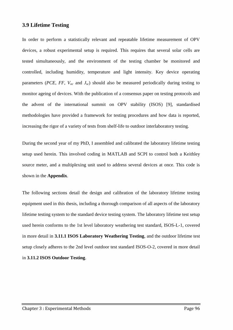
Chapter 3 : Experimental Methods Page 96
3.9 Lifetime Testing
In order to perform a statistically relevant and repeatable lifetime measurement of OPV
devices, a robust experimental setup is required. This requires that several solar cells are
tested simultaneously, and the environment of the testing chamber be monitored and
controlled, including humidity, temperature and light intensity. Key device operating
parameters (PCE, FF, Voc and Jsc) should also be measured periodically during testing to
monitor ageing of devices. With the publication of a consensus paper on testing protocols and
the advent of the international summit on OPV stability (ISOS) [9], standardised
methodologies have provided a framework for testing procedures and how data is reported,
increasing the rigor of a variety of tests from shelf-life to outdoor interlaboratory testing.
During the second year of my PhD, I assembled and calibrated the laboratory lifetime testing
setup used herein. This involved coding in MATLAB and SCPI to control both a Keithley
source meter, and a multiplexing unit used to address several devices at once. This code is
shown in the Appendix.
The following sections detail the design and calibration of the laboratory lifetime testing
equipment used in this thesis, including a thorough comparison of all aspects of the laboratory
lifetime testing system to the standard device testing system. The laboratory lifetime test setup
used herein conforms to the 1st level laboratory weathering test standard, ISOS-L-1, covered
in more detail in 3.11.1 ISOS Laboratory Weathering Testing, and the outdoor lifetime test
setup closely adheres to the 2nd level outdoor test standard ISOS-O-2, covered in more detail
in 3.11.2 ISOS Outdoor Testing.
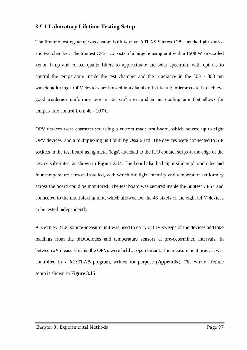
Chapter 3 : Experimental Methods Page 97
3.9.1 Laboratory Lifetime Testing Setup
The lifetime testing setup was custom built with an ATLAS Suntest CPS+ as the light source
and test chamber. The Suntest CPS+ consists of a large housing unit with a 1500 W air-cooled
xenon lamp and coated quartz filters to approximate the solar spectrum, with options to
control the temperature inside the test chamber and the irradiance in the 300 - 800 nm
wavelength range. OPV devices are housed in a chamber that is fully mirror coated to achieve
good irradiance uniformity over a 560 cm2 area, and an air cooling unit that allows for
temperature control from 40 - 100oC.
OPV devices were characterised using a custom-made test board, which housed up to eight
OPV devices, and a multiplexing unit built by Ossila Ltd. The devices were connected to SIP
sockets in the test board using metal 'legs', attached to the ITO contact strips at the edge of the
device substrates, as shown in Figure 3.14. The board also had eight silicon photodiodes and
four temperature sensors installed, with which the light intensity and temperature uniformity
across the board could be monitored. The test board was secured inside the Suntest CPS+ and
connected to the multiplexing unit, which allowed for the 48 pixels of the eight OPV devices
to be tested independently.
A Keithley 2400 source-measure unit was used to carry out IV sweeps of the devices and take
readings from the photodiodes and temperature sensors at pre-determined intervals. In
between JV measurements the OPVs were held at open circuit. The measurement process was
controlled by a MATLAB program, written for purpose (Appendix). The whole lifetime
setup is shown in Figure 3.15.
Chapter 3 : Experimental Methods Page 98
Figure 3.14 (a) OPV device with electrical connection 'legs' attached to the ITO contact strips
at the edge of the substrate. (b) Shows the circuit board into which the OPV devices were
inserted, with devices number S1, S2 etc. The test board measured 100 x 100 mm.
Figure 3.15 Image of the lifetime testing setup with key features labelled.
Chapter 3 : Experimental Methods Page 99
Due to the design of the test board and the reliance on reflected light to achieve 1 sun
intensity, no aperture masks were used when characterizing devices in the lifetime tester. This
introduced errors in measurement that are covered in more detail in 3.9.6 Pixel Size
Variation.
3.9.2 Light Source and Spectrum
The choice of light source is important for lifetime testing of OPVs, and several factors have
to be taken into account: cost, lifetime, uniformity of illumination, and match to the solar
spectrum. The three types of lamp that are commonly used for OPV lifetime testing are
sulphur plasma, xenon arc and metal halide global lamps. All need to be fitted with daylight
filters to better simulate the solar spectrum. The Suntest CPS+ system with its xenon arc lamp
and appropriate daylight filters was chosen for the lifetime testing system due to its good
match to the solar spectrum in the UV, visible and infrared as shown in Figure 3.16. The
spectrum was measured using a calibrated StellarNet Inc. Blue Wave USB spectrometer, and
is consistent with spectra from other xenon lamps reported in the literature [9]. It can be seen
that although there is a reasonably good match to the solar spectrum between 350 - 600 nm
range, the xenon bulb is less powerful in the 600 nm + range. However, as PCDTBT (the
polymer used in lifetime measurements in this thesis) absorbs in the 350 - 700 nm range, this
does not result in significant differences in measured photocurrent, discussed in more detail in
3.9.3 JV Mismatch.
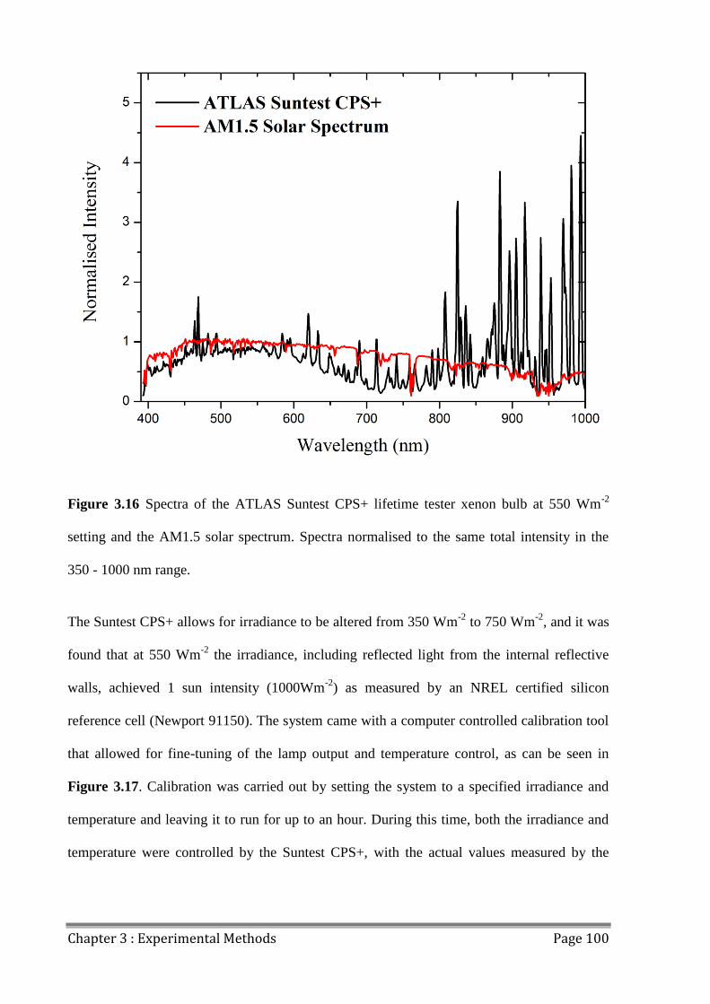
Chapter 3 : Experimental Methods Page 100
Figure 3.16 Spectra of the ATLAS Suntest CPS+ lifetime tester xenon bulb at 550 Wm-2
setting and the AM1.5 solar spectrum. Spectra normalised to the same total intensity in the
350 - 1000 nm range.
The Suntest CPS+ allows for irradiance to be altered from 350 Wm-2
to 750 Wm-2
, and it was
found that at 550 Wm-2
the irradiance, including reflected light from the internal reflective
walls, achieved 1 sun intensity (1000Wm-2
) as measured by an NREL certified silicon
reference cell (Newport 91150). The system came with a computer controlled calibration tool
that allowed for fine-tuning of the lamp output and temperature control, as can be seen in
Figure 3.17. Calibration was carried out by setting the system to a specified irradiance and
temperature and leaving it to run for up to an hour. During this time, both the irradiance and
temperature were controlled by the Suntest CPS+, with the actual values measured by the
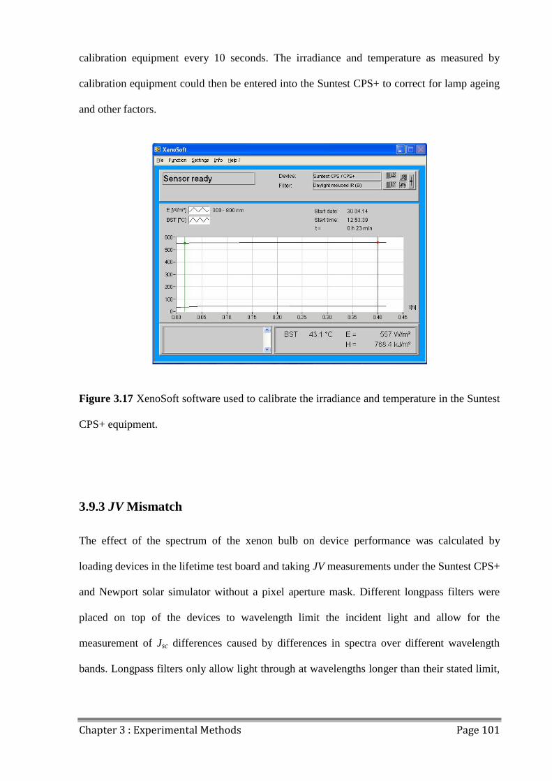
Chapter 3 : Experimental Methods Page 101
calibration equipment every 10 seconds. The irradiance and temperature as measured by
calibration equipment could then be entered into the Suntest CPS+ to correct for lamp ageing
and other factors.
Figure 3.17 XenoSoft software used to calibrate the irradiance and temperature in the Suntest
CPS+ equipment.
3.9.3 JV Mismatch
The effect of the spectrum of the xenon bulb on device performance was calculated by
loading devices in the lifetime test board and taking JV measurements under the Suntest CPS+
and Newport solar simulator without a pixel aperture mask. Different longpass filters were
placed on top of the devices to wavelength limit the incident light and allow for the
measurement of Jsc differences caused by differences in spectra over different wavelength
bands. Longpass filters only allow light through at wavelengths longer than their stated limit,
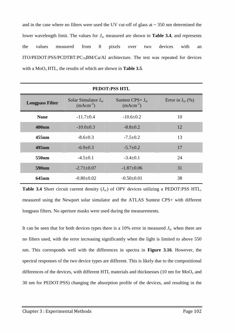
Chapter 3 : Experimental Methods Page 102
and in the case where no filters were used the UV cut-off of glass at ~ 350 nm determined the
lower wavelength limit. The values for Jsc measured are shown in Table 3.4, and represents
the values measured from 8 pixels over two devices with an
ITO/PEDOT:PSS/PCDTBT:PC70BM/Ca/Al architecture. The test was repeated for devices
with a MoOx HTL, the results of which are shown in Table 3.5.
PEDOT:PSS HTL
Longpass Filter Solar Simulator Jsc
(mAcm-2
)
Suntest CPS+ Jsc
(mAcm-2
)
Error in Jsc (%)
None -11.7±0.4 -10.6±0.2 10
400nm -10.0±0.3 -8.8±0.2 12
455nm -8.6±0.3 -7.5±0.2 13
495nm -6.9±0.3 -5.7±0.2 17
550nm -4.5±0.1 -3.4±0.1 24
590nm -2.71±0.07 -1.87±0.06 31
645nm -0.80±0.02 -0.50±0.01 38
Table 3.4 Short circuit current density (Jsc) of OPV devices utilizing a PEDOT:PSS HTL,
measured using the Newport solar simulator and the ATLAS Suntest CPS+ with different
longpass filters. No aperture masks were used during the measurements.
It can be seen that for both devices types there is a 10% error in measured Jsc when there are
no filters used, with the error increasing significantly when the light is limited to above 550
nm. This corresponds well with the differences in spectra in Figure 3.16. However, the
spectral responses of the two device types are different. This is likely due to the compositional
differences of the devices, with different HTL materials and thicknesses (10 nm for MoOx and
30 nm for PEDOT:PSS) changing the absorption profile of the devices, and resulting in the
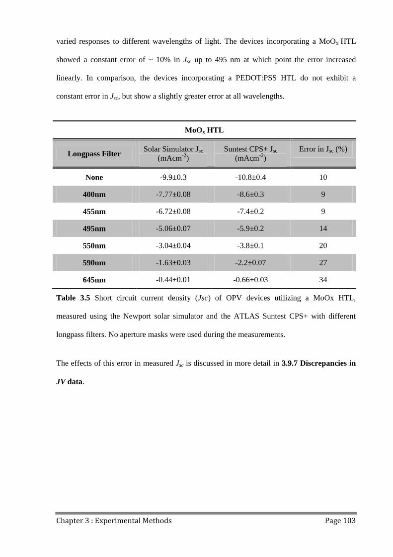
Chapter 3 : Experimental Methods Page 103
varied responses to different wavelengths of light. The devices incorporating a MoOx HTL
showed a constant error of ~ 10% in Jsc up to 495 nm at which point the error increased
linearly. In comparison, the devices incorporating a PEDOT:PSS HTL do not exhibit a
constant error in Jsc, but show a slightly greater error at all wavelengths.
MoOx HTL
Longpass Filter Solar Simulator Jsc
(mAcm-2
)
Suntest CPS+ Jsc
(mAcm-2
)
Error in Jsc (%)
None -9.9±0.3 -10.8±0.4 10
400nm -7.77±0.08 -8.6±0.3 9
455nm -6.72±0.08 -7.4±0.2 9
495nm -5.06±0.07 -5.9±0.2 14
550nm -3.04±0.04 -3.8±0.1 20
590nm -1.63±0.03 -2.2±0.07 27
645nm -0.44±0.01 -0.66±0.03 34
Table 3.5 Short circuit current density (Jsc) of OPV devices utilizing a MoOx HTL,
measured using the Newport solar simulator and the ATLAS Suntest CPS+ with different
longpass filters. No aperture masks were used during the measurements.
The effects of this error in measured Jsc is discussed in more detail in 3.9.7 Discrepancies in
JV data.
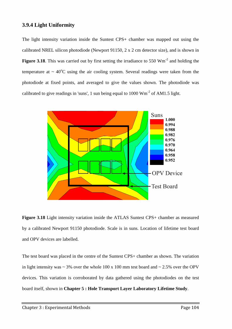
Chapter 3 : Experimental Methods Page 104
3.9.4 Light Uniformity
The light intensity variation inside the Suntest CPS+ chamber was mapped out using the
calibrated NREL silicon photodiode (Newport 91150, 2 x 2 cm detector size), and is shown in
Figure 3.18. This was carried out by first setting the irradiance to 550 Wm-2
and holding the
temperature at ~ 40oC using the air cooling system. Several readings were taken from the
photodiode at fixed points, and averaged to give the values shown. The photodiode was
calibrated to give readings in 'suns', 1 sun being equal to 1000 Wm-2
of AM1.5 light.
Figure 3.18 Light intensity variation inside the ATLAS Suntest CPS+ chamber as measured
by a calibrated Newport 91150 photodiode. Scale is in suns. Location of lifetime test board
and OPV devices are labelled.
The test board was placed in the centre of the Suntest CPS+ chamber as shown. The variation
in light intensity was ~ 3% over the whole 100 x 100 mm test board and ~ 2.5% over the OPV
devices. This variation is corroborated by data gathered using the photodiodes on the test
board itself, shown in Chapter 5 : Hole Transport Layer Laboratory Lifetime Study.
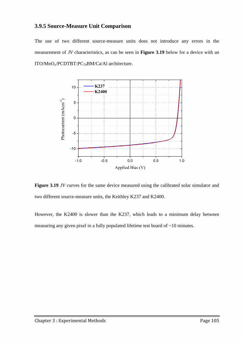
Chapter 3 : Experimental Methods Page 105
3.9.5 Source-Measure Unit Comparison
The use of two different source-measure units does not introduce any errors in the
measurement of JV characteristics, as can be seen in Figure 3.19 below for a device with an
ITO/MoOx/PCDTBT:PC70BM/Ca/Al architecture.
Figure 3.19 JV curves for the same device measured using the calibrated solar simulator and
two different source-measure units, the Keithley K237 and K2400.
However, the K2400 is slower than the K237, which leads to a minimum delay between
measuring any given pixel in a fully populated lifetime test board of ~10 minutes.

Chapter 3 : Experimental Methods Page 106
3.9.6 Pixel Size Variation
As previously stated, the evaporation of the top contact defines the pixel area. For the
evaporation masks used, as shown in Figure 3.4, the size of the depression in which the
substrate fits has a tolerance of 100 µm to allow for small variations in substrate size and ease
of use. This means that the position of the substrates in the mask can differ by up to 200 µm
in both the x and y directions. Whilst this does not have an effect on pixel size if the offset is
in the y axis, it can have a significant effect on pixel size if the substrate is not perfectly
central in the x direction. This is illustrated in Figure 3.20.
Figure 3.20 Variation in pixel size caused by misalignment of the top contact evaporation
mask. The area in red is identical in size in all images. (a) Shows the pixel size when the
substrate is perfectly aligned, (b) shows an x offset which increases the pixel size and (c)
shows an x offset that decreases the pixel size.
The pixel size when the substrate and mask are perfectly aligned, as in Figure 3.20 (a), is
0.04 cm2. However, due to the 100 µm tolerance in the mask design, the actual area can be as
large as 0.042 cm2 (Figure 3.20 (b)) and as little as 0.038 cm
2 (Figure 3.20 (c)). When using
an aperture mask this does not result in measurement errors, as the size of the apertures are
smaller than even the minimum possible pixel size, at 0.0261 cm2. Unfortunately, when not
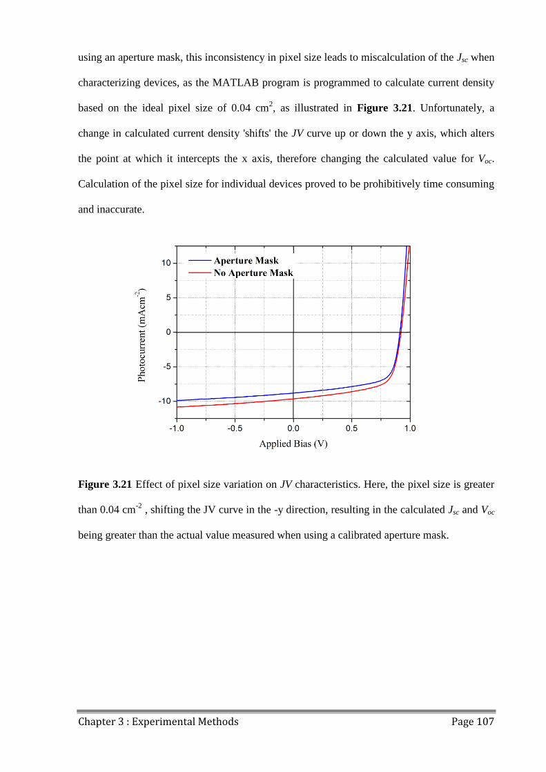
Chapter 3 : Experimental Methods Page 107
using an aperture mask, this inconsistency in pixel size leads to miscalculation of the Jsc when
characterizing devices, as the MATLAB program is programmed to calculate current density
based on the ideal pixel size of 0.04 cm2, as illustrated in Figure 3.21. Unfortunately, a
change in calculated current density 'shifts' the JV curve up or down the y axis, which alters
the point at which it intercepts the x axis, therefore changing the calculated value for Voc.
Calculation of the pixel size for individual devices proved to be prohibitively time consuming
and inaccurate.
Figure 3.21 Effect of pixel size variation on JV characteristics. Here, the pixel size is greater
than 0.04 cm-2
, shifting the JV curve in the -y direction, resulting in the calculated Jsc and Voc
being greater than the actual value measured when using a calibrated aperture mask.
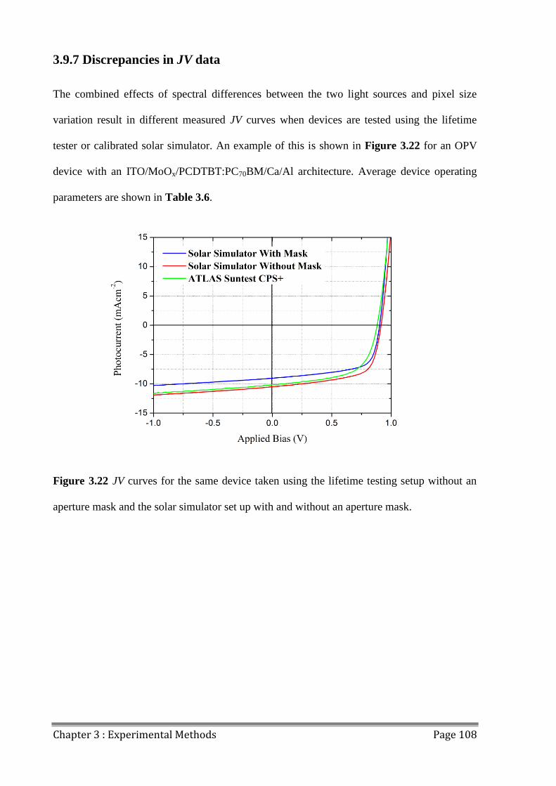
Chapter 3 : Experimental Methods Page 108
3.9.7 Discrepancies in JV data
The combined effects of spectral differences between the two light sources and pixel size
variation result in different measured JV curves when devices are tested using the lifetime
tester or calibrated solar simulator. An example of this is shown in Figure 3.22 for an OPV
device with an ITO/MoOx/PCDTBT:PC70BM/Ca/Al architecture. Average device operating
parameters are shown in Table 3.6.
Figure 3.22 JV curves for the same device taken using the lifetime testing setup without an
aperture mask and the solar simulator set up with and without an aperture mask.
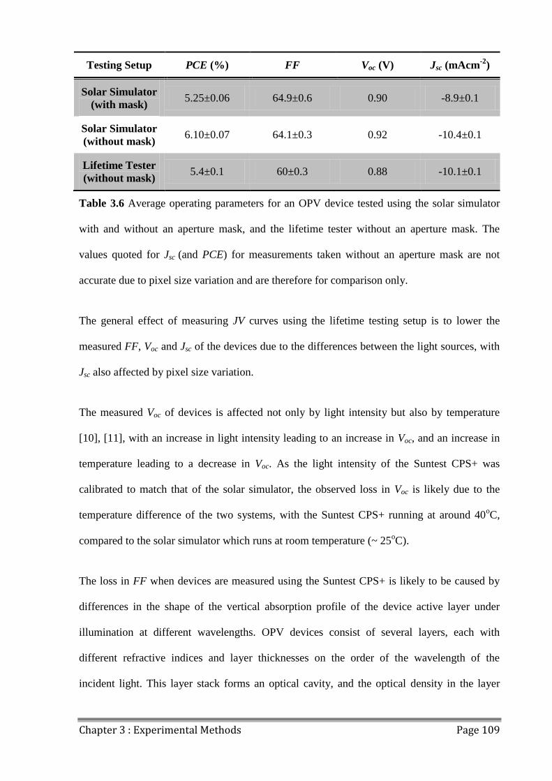
Chapter 3 : Experimental Methods Page 109
Testing Setup PCE (%) FF Voc (V) Jsc (mAcm-2
)
Solar Simulator
(with mask) 5.25±0.06 64.9±0.6 0.90 -8.9±0.1
Solar Simulator
(without mask) 6.10±0.07 64.1±0.3 0.92 -10.4±0.1
Lifetime Tester
(without mask) 5.4±0.1 60±0.3 0.88 -10.1±0.1
Table 3.6 Average operating parameters for an OPV device tested using the solar simulator
with and without an aperture mask, and the lifetime tester without an aperture mask. The
values quoted for Jsc (and PCE) for measurements taken without an aperture mask are not
accurate due to pixel size variation and are therefore for comparison only.
The general effect of measuring JV curves using the lifetime testing setup is to lower the
measured FF, Voc and Jsc of the devices due to the differences between the light sources, with
Jsc also affected by pixel size variation.
The measured Voc of devices is affected not only by light intensity but also by temperature
[10], [11], with an increase in light intensity leading to an increase in Voc, and an increase in
temperature leading to a decrease in Voc. As the light intensity of the Suntest CPS+ was
calibrated to match that of the solar simulator, the observed loss in Voc is likely due to the
temperature difference of the two systems, with the Suntest CPS+ running at around 40oC,
compared to the solar simulator which runs at room temperature (~ 25oC).
The loss in FF when devices are measured using the Suntest CPS+ is likely to be caused by
differences in the shape of the vertical absorption profile of the device active layer under
illumination at different wavelengths. OPV devices consist of several layers, each with
different refractive indices and layer thicknesses on the order of the wavelength of the
incident light. This layer stack forms an optical cavity, and the optical density in the layer

Chapter 3 : Experimental Methods Page 110
differs for different wavelengths [12]–[14]. Varying the incident light spectrum has an effect
on the generation and transport properties of carriers at different depths in the active layer due
to variations in the optical density in the active layer. This has an effect on the shape of the JV
curve, which manifests as a change in FF [15], [16]. As the spectrum of the xenon lamp in the
Suntest CPS+ is different to that of the solar spectrum produced by the solar simulator, as
shown in 3.9.2 Light Source and Spectrum, this mechanism is likely the cause of the loss of
measured FF.
These factors combine to give a different measured device efficiency in the lifetime testing
setup when compared to that measured using the solar simulator. It has been discovered that
this effect varies in magnitude depending on the device composition and architecture, due to
the different layer thicknesses of the materials used leading to different absorption
characteristics.
Due to this discrepancy, only JV data from the calibrated solar simulator is shown in results
chapters, and any data collected from the lifetime tester is normalised to remove any errors
introduced by the setup.
3.10 Outdoor Lifetime Testing
In addition to laboratory lifetime testing, OPV devices were also mounted in a lifetime testing
setup on the roof of the Department of Physics at the University of Sheffield, England, UK.
The outdoor lifetime testing setup is shown in Figure 3.23, and included three environmental
chambers, each housing an OPV test board (with space for 8 devices) identical to that used for
laboratory lifetime testing shown in Figure 3.14 (b). The environmental chambers consisted
Chapter 3 : Experimental Methods Page 111
of a milled aluminium block with a glass cover, sealed with an O-ring and filled with an
overpressure of nitrogen to prevent air ingress into the chamber. The overpressure of nitrogen
was maintained throughout the testing. A weatherproof metal case contained the electronics
and the computer used to control the measurement of the JV characteristics of the OPV
devices and monitor the temperature inside the environmental chambers. A National
Instruments PXI-4132 source measure unit was used to measure the JV characteristics of the
devices over the -1.0 to 1.0 V range in 0.02V steps every ~ 5 minutes, and a multiplexing unit
was used to allow for individual measurement of the 144 pixels of the 24 devices. In between
measurements, the devices were kept at open circuit as with the laboratory lifetime test.
The light intensity was monitored using a SPN1 Sunshine Pyranometer, which measured and
recorded the total and diffuse irradiance at the point of each JV measurement. The readings
from the four temperature sensors were also recorded at the point of each JV measurement.
This allowed for the effects of both irradiance and temperature on device performance every 5
minutes to be tracked throughout the course of the experiment.
The test protocol used herein is of the outdoor testing type, and closely adheres to the second
level of testing rigor, ISOS-O-2, the requirements of which are covered 3.11.2 ISOS Outdoor
Testing.
The device test chamber was mounted on a fixed platform facing south with a 30o orientation
to maximise incident light.
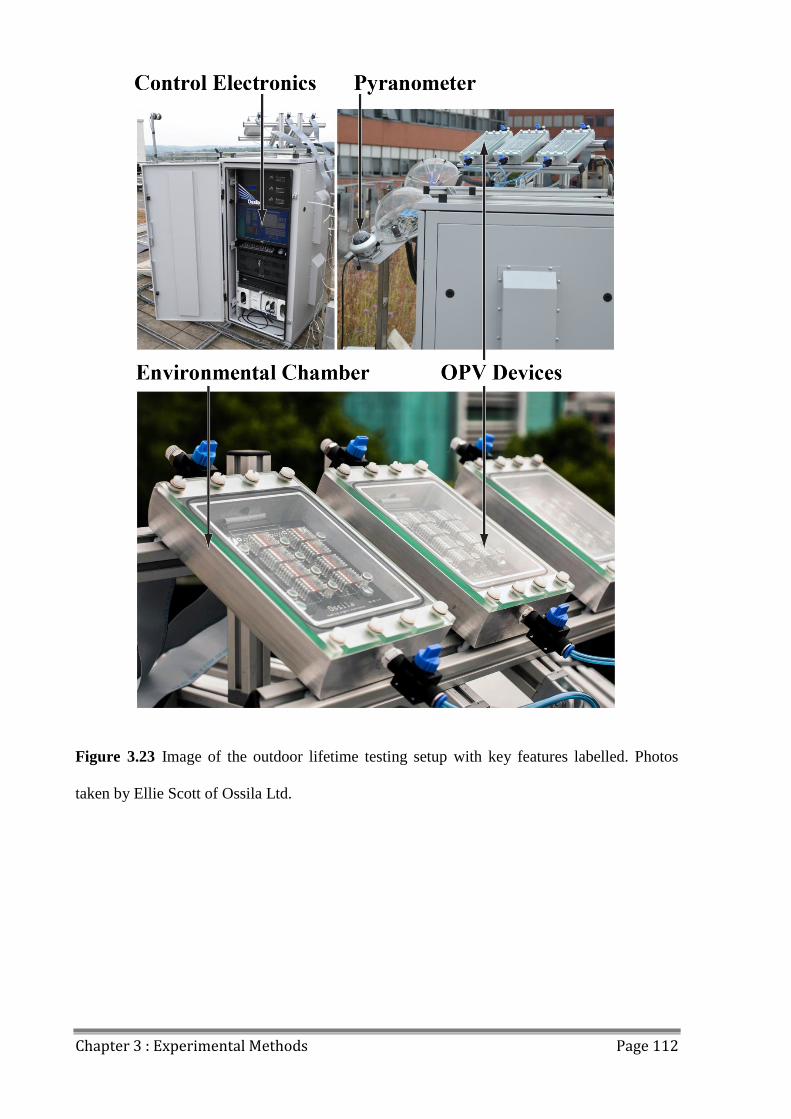
Chapter 3 : Experimental Methods Page 112
Figure 3.23 Image of the outdoor lifetime testing setup with key features labelled. Photos
taken by Ellie Scott of Ossila Ltd.
Chapter 3 : Experimental Methods Page 113
3.11 Lifetime Reporting
The most widely used metric used to describe OPV device lifetime is 'T80 lifetime', as
previously discussed in 2.9.6 Decay Behaviour. This is defined as the period of time that
elapses between the initial stabilised performance after burn-in, and the point at which 80% of
this efficiency has been reached. Along with this value, the time evolution of device JV
parameters (PCE, FF, Voc and Jsc) give an indication of device stability. Other
characterization methods, such as LBIC, ELM and absorbance spectroscopy, give valuable
insight into degradation mechanisms that cause the loss in device performance.
With the advent of the annual International Summit on OPV Stability (ISOS) and the
publication of a consensus paper on testing protocols [9], the reporting of OPV device
stability and lifetime has been standardised. There are several tests commonly used for
lifetime testing, including shelf-life, thermal cycling, outdoor and laboratory weathering
testing, each with three levels of increasing rigor. The test protocol used herein for indoor
testing is of the laboratory weathering type, and conforms to the first level of testing rigor,
ISOS-L-1, the requirements of which are covered in the next section. The test protocol used
for outdoor testing conforms closely to the ISOS-O-2 requirements.
3.11.1 ISOS Laboratory Weathering Testing
Table 3.7 shows the basic requirements for the three different levels of ISOS laboratory
weathering testing. In all cases, the light source needs to match the solar spectrum as closely
as possible and other parameters, such as temperature and humidity, need to be monitored or
controlled.
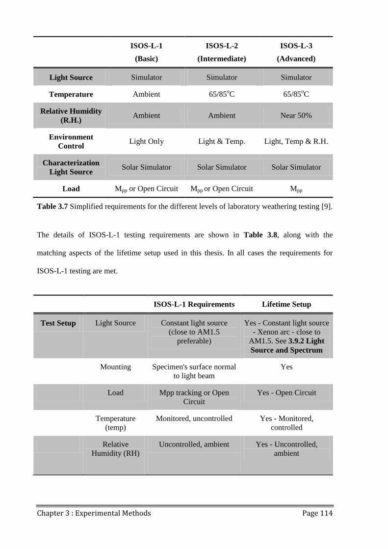
Chapter 3 : Experimental Methods Page 114
ISOS-L-1
(Basic)
ISOS-L-2
(Intermediate)
ISOS-L-3
(Advanced)
Light Source Simulator Simulator Simulator
Temperature Ambient 65/85oC 65/85
oC
Relative Humidity
(R.H.) Ambient Ambient Near 50%
Environment
Control Light Only Light & Temp. Light, Temp & R.H.
Characterization
Light Source Solar Simulator Solar Simulator Solar Simulator
Load Mpp or Open Circuit Mpp or Open Circuit Mpp
Table 3.7 Simplified requirements for the different levels of laboratory weathering testing [9].
The details of ISOS-L-1 testing requirements are shown in Table 3.8, along with the
matching aspects of the lifetime setup used in this thesis. In all cases the requirements for
ISOS-L-1 testing are met.
ISOS-L-1 Requirements Lifetime Setup
Test Setup Light Source Constant light source
(close to AM1.5
preferable)
Yes - Constant light source
- Xenon arc - close to
AM1.5. See 3.9.2 Light
Source and Spectrum
Mounting Specimen's surface normal
to light beam
Yes
Load Mpp tracking or Open
Circuit
Yes - Open Circuit
Temperature
(temp)
Monitored, uncontrolled Yes - Monitored,
controlled
Relative
Humidity (RH)
Uncontrolled, ambient Yes - Uncontrolled,
ambient
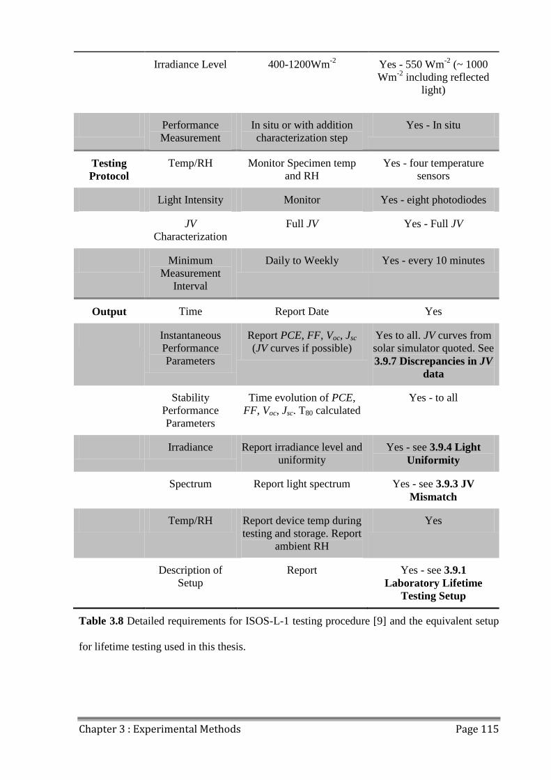
Chapter 3 : Experimental Methods Page 115
Irradiance Level
400-1200Wm-2
Yes - 550 Wm-2
(~ 1000
Wm-2
including reflected
light)
Performance
Measurement
In situ or with addition
characterization step
Yes - In situ
Testing
Protocol
Temp/RH Monitor Specimen temp
and RH
Yes - four temperature
sensors
Light Intensity Monitor Yes - eight photodiodes
JV
Characterization
Full JV Yes - Full JV
Minimum
Measurement
Interval
Daily to Weekly Yes - every 10 minutes
Output Time Report Date Yes
Instantaneous
Performance
Parameters
Report PCE, FF, Voc, Jsc
(JV curves if possible)
Yes to all. JV curves from
solar simulator quoted. See
3.9.7 Discrepancies in JV
data
Stability
Performance
Parameters
Time evolution of PCE,
FF, Voc, Jsc. T80 calculated
Yes - to all
Irradiance Report irradiance level and
uniformity
Yes - see 3.9.4 Light
Uniformity
Spectrum Report light spectrum Yes - see 3.9.3 JV
Mismatch
Temp/RH Report device temp during
testing and storage. Report
ambient RH
Yes
Description of
Setup
Report Yes - see 3.9.1
Laboratory Lifetime
Testing Setup
Table 3.8 Detailed requirements for ISOS-L-1 testing procedure [9] and the equivalent setup
for lifetime testing used in this thesis.
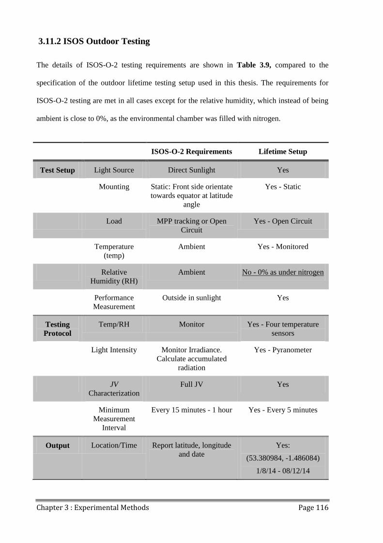
Chapter 3 : Experimental Methods Page 116
3.11.2 ISOS Outdoor Testing
The details of ISOS-O-2 testing requirements are shown in Table 3.9, compared to the
specification of the outdoor lifetime testing setup used in this thesis. The requirements for
ISOS-O-2 testing are met in all cases except for the relative humidity, which instead of being
ambient is close to 0%, as the environmental chamber was filled with nitrogen.
ISOS-O-2 Requirements Lifetime Setup
Test Setup Light Source Direct Sunlight Yes
Mounting Static: Front side orientate
towards equator at latitude
angle
Yes - Static
Load MPP tracking or Open
Circuit
Yes - Open Circuit
Temperature
(temp)
Ambient Yes - Monitored
Relative
Humidity (RH)
Ambient No - 0% as under nitrogen
Performance
Measurement
Outside in sunlight Yes
Testing
Protocol
Temp/RH Monitor Yes - Four temperature
sensors
Light Intensity Monitor Irradiance.
Calculate accumulated
radiation
Yes - Pyranometer
JV
Characterization
Full JV Yes
Minimum
Measurement
Interval
Every 15 minutes - 1 hour Yes - Every 5 minutes
Output Location/Time Report latitude, longitude
and date
Yes:
(53.380984, -1.486084)
1/8/14 - 08/12/14
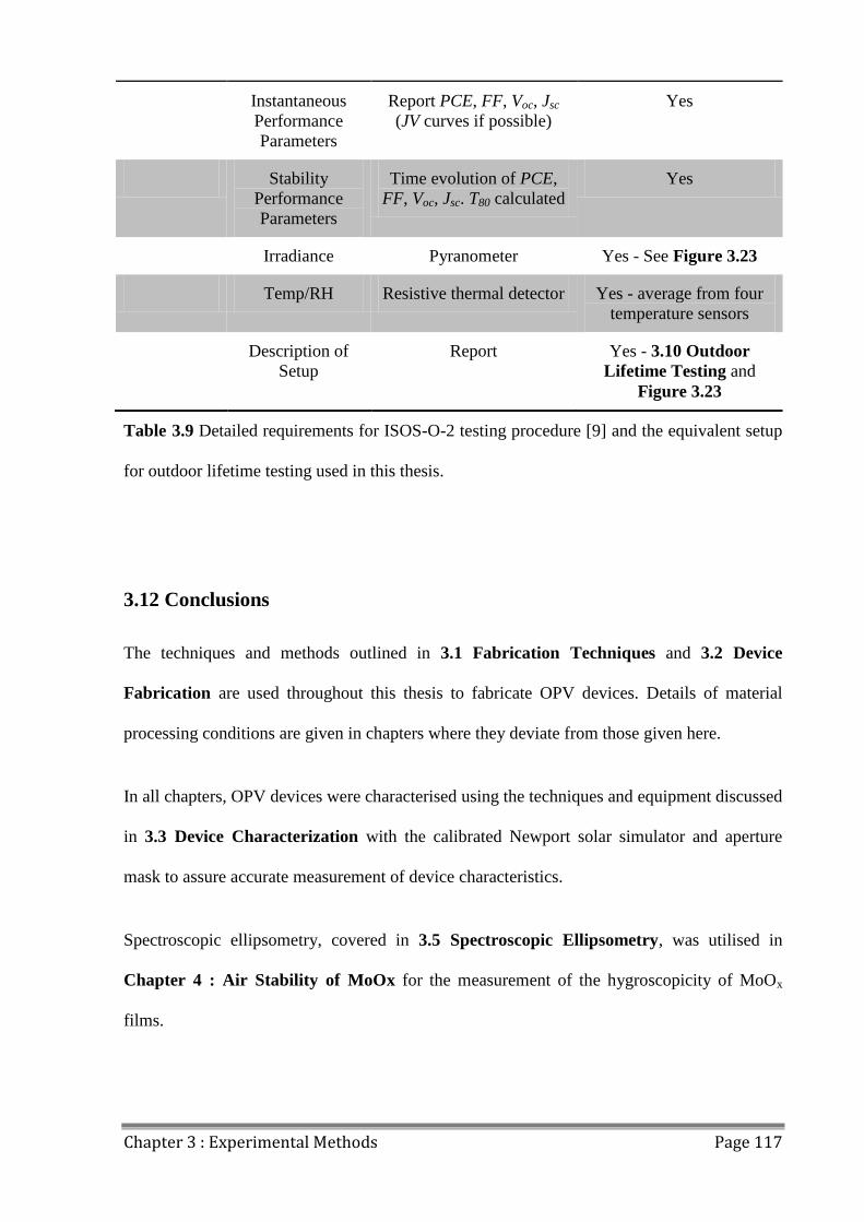
Chapter 3 : Experimental Methods Page 117
Instantaneous
Performance
Parameters
Report PCE, FF, Voc, Jsc
(JV curves if possible)
Yes
Stability
Performance
Parameters
Time evolution of PCE,
FF, Voc, Jsc. T80 calculated
Yes
Irradiance Pyranometer Yes - See Figure 3.23
Temp/RH Resistive thermal detector Yes - average from four
temperature sensors
Description of
Setup
Report Yes - 3.10 Outdoor
Lifetime Testing and
Figure 3.23
Table 3.9 Detailed requirements for ISOS-O-2 testing procedure [9] and the equivalent setup
for outdoor lifetime testing used in this thesis.
3.12 Conclusions
The techniques and methods outlined in 3.1 Fabrication Techniques and 3.2 Device
Fabrication are used throughout this thesis to fabricate OPV devices. Details of material
processing conditions are given in chapters where they deviate from those given here.
In all chapters, OPV devices were characterised using the techniques and equipment discussed
in 3.3 Device Characterization with the calibrated Newport solar simulator and aperture
mask to assure accurate measurement of device characteristics.
Spectroscopic ellipsometry, covered in 3.5 Spectroscopic Ellipsometry, was utilised in
Chapter 4 : Air Stability of MoOx for the measurement of the hygroscopicity of MoOx
films.
Chapter 3 : Experimental Methods Page 118
For the laboratory lifetime test of OPV devices in Chapter 5 : Hole Transport Layer
Laboratory Lifetime Study, the lifetime test equipment detailed in 3.9 Lifetime Testing was
used. The discrepancy in JV characterisation between the laboratory lifetime testing system
and Newport solar simulator, discussed in 3.9.7 Discrepancies in JV data, are accounted for
in all results.
LBIC and ELM techniques, 3.7 Laser Beam Induced Current Mapping (LBIC) and 3.8
Electroluminescence Mapping (ELM) respectively, were used to detect defects formed in
OPV devices aged in the laboratory lifetime testing setup in Chapter 5 : Hole Transport
Layer Laboratory Lifetime Study.
In Chapter 6 : Polymer Air Processing, absorbance spectroscopy and EQE measurements,
discussed in 3.4 Absorbance Spectroscopy and 3.6 External Quantum Efficiency (EQE)
respectively, were used to investigate the effects spin-coating the active layer of OPV devices
in air.
Finally, in Chapter 7 : Outdoor Lifetime Testing, the outdoor lifetime testing setup detailed
in 3.10 Outdoor Lifetime Testing was used to test the response of optimised OPV devices to
ageing in varying illumination and thermal conditions on a rooftop in Sheffield, England, UK
over the course of 4 months.
Chapter 3 : Experimental Methods Page 119
3.13 References
[1] Y. Liang, Z. Xu, J. Xia, S.-T. Tsai, Y. Wu, G. Li, C. Ray, and L. Yu, “For the bright
future-bulk heterojunction polymer solar cells with power conversion efficiency of 7.4%.,”
Adv. Mater., vol. 22, no. 20, pp. E135–8, May 2010.
[2] J. D. Servaites, S. Yeganeh, T. J. Marks, and M. A. Ratner, “Efficiency Enhancement
in Organic Photovoltaic Cells: Consequences of Optimizing Series Resistance,” Adv. Funct.
Mater., vol. 20, no. 1, pp. 97–104, Jan. 2010.
[3] R. A. Street, K. W. Song, and S. Cowan, “Influence of series resistance on the
photocurrent analysis of organic solar cells,” Org. Electron., vol. 12, no. 2, pp. 244–248, Feb.
2011.
[4] T. Kirchartz, F. Deledalle, P. S. Tuladhar, J. R. Durrant, and J. Nelson, “On the
differences between dark and light ideality factor in polymer:Fullerene solar cells,” J. Phys.
Chem. Lett., vol. 4, no. 14, pp. 2371–2376, Jul. 2013.
[5] T. M. Clarke, A. Ballantyne, S. Shoaee, Y. W. Soon, W. Duffy, M. Heeney, I.
McCulloch, J. Nelson, and J. R. Durrant, “Analysis of charge photogeneration as a key
determinant of photocurrent density in polymer: fullerene solar cells.,” Adv. Mater., vol. 22,
no. 46, pp. 5287–91, Dec. 2010.
[6] G. F. A. Dibb, F. C. Jamieson, A. Maurano, J. Nelson, and J. R. Durrant, “Limits on
the Fill Factor in Organic Photovoltaics: Distinguishing Nongeminate and Geminate
Recombination Mechanisms,” J. Phys. Chem. Lett., vol. 4, no. 5, pp. 803–808, Mar. 2013.
Chapter 3 : Experimental Methods Page 120
[7] J. M. Kroon, M. M. Wienk, W. J. H. Verhees, and J. C. Hummelen, “Accurate
efficiency determination and stability studies of conjugated polymer/fullerene solar cells,”
Thin Solid Films, vol. 403–404, pp. 223–228, Feb. 2002.
[8] M. T. Lloyd, C. H. Peters, A. Garcia, I. V. Kauvar, J. J. Berry, M. O. Reese, M. D.
McGehee, D. S. Ginley, and D. C. Olson, “Influence of the hole-transport layer on the initial
behavior and lifetime of inverted organic photovoltaics,” Sol. Energy Mater. Sol. Cells, vol.
95, no. 5, pp. 1382–1388, May 2011.
[9] M. O. Reese, S. A. Gevorgyan, M. Jørgensen, E. Bundgaard, S. R. Kurtz, D. S.
Ginley, D. C. Olson, M. T. Lloyd, P. Morvillo, E. A. Katz, A. Elschner, O. Haillant, T. R.
Currier, V. Shrotriya, M. Hermenau, M. Riede, K. R. Kirov, G. Trimmel, T. Rath, O. Inganäs,
F. Zhang, M. Andersson, K. Tvingstedt, M. Lira-Cantu, D. Laird, C. McGuiness, S. (Jimmy)
Gowrisanker, M. Pannone, M. Xiao, J. Hauch, R. Steim, D. M. DeLongchamp, R. Rösch, H.
Hoppe, N. Espinosa, A. Urbina, G. Yaman-Uzunoglu, J.-B. Bonekamp, A. J. J. M. van
Breemen, C. Girotto, E. Voroshazi, and F. C. Krebs, “Consensus stability testing protocols for
organic photovoltaic materials and devices,” Sol. Energy Mater. Sol. Cells, vol. 95, no. 5, pp.
1253–1267, May 2011.
[10] G. Garcia-Belmonte, “Temperature dependence of open-circuit voltage in organic
solar cells from generation–recombination kinetic balance,” Sol. Energy Mater. Sol. Cells,
vol. 94, no. 12, pp. 2166–2169, Dec. 2010.
[11] A. Manor, E. A. Katz, R. Andriessen, and Y. Galagan, “Study of organic photovoltaics
by localized concentrated sunlight: Towards optimization of charge collection in large-area
solar cells,” Appl. Phys. Lett., vol. 99, no. 17, p. 173305, 2011.
Chapter 3 : Experimental Methods Page 121
[12] J. Y. Kim, S. H. Kim, H.-H. Lee, K. Lee, W. Ma, X. Gong, and A. J. Heeger, “New
Architecture for High-Efficiency Polymer Photovoltaic Cells Using Solution-Based Titanium
Oxide as an Optical Spacer,” Adv. Mater., vol. 18, no. 5, pp. 572–576, Mar. 2006.
[13] B. Valle, S. Loser, J. W. Hennek, V. DeGeorge, C. Klosterman, J. H. Andrews, K. D.
Singer, and T. J. Marks, “Spectral aspects of cavity tuned absorption in organic photovoltaic
films.,” Opt. Express, vol. 20 Suppl 6, no. November, pp. A954–63, Nov. 2012.
[14] X. Zhao, Z. Li, T. Zhu, B. Mi, Z. Gao, and W. Huang, “Structure optimization of
organic planar heterojunction solar cells,” J. Phys. D. Appl. Phys., vol. 46, no. 19, p. 195105,
May 2013.
[15] J. Mescher, N. Christ, S. Kettlitz, A. Colsmann, and U. Lemmer, “Influence of the
spatial photocarrier generation profile on the performance of organic solar cells,” Appl. Phys.
Lett., vol. 101, no. 7, p. 073301, Aug. 2012.
[16] J. D. Kotlarski and P. W. M. Blom, “Impact of unbalanced charge transport on the
efficiency of normal and inverted solar cells,” Appl. Phys. Lett., vol. 100, no. 1, p. 013306,
2012.

Chapter 3 : Experimental Methods Page 122
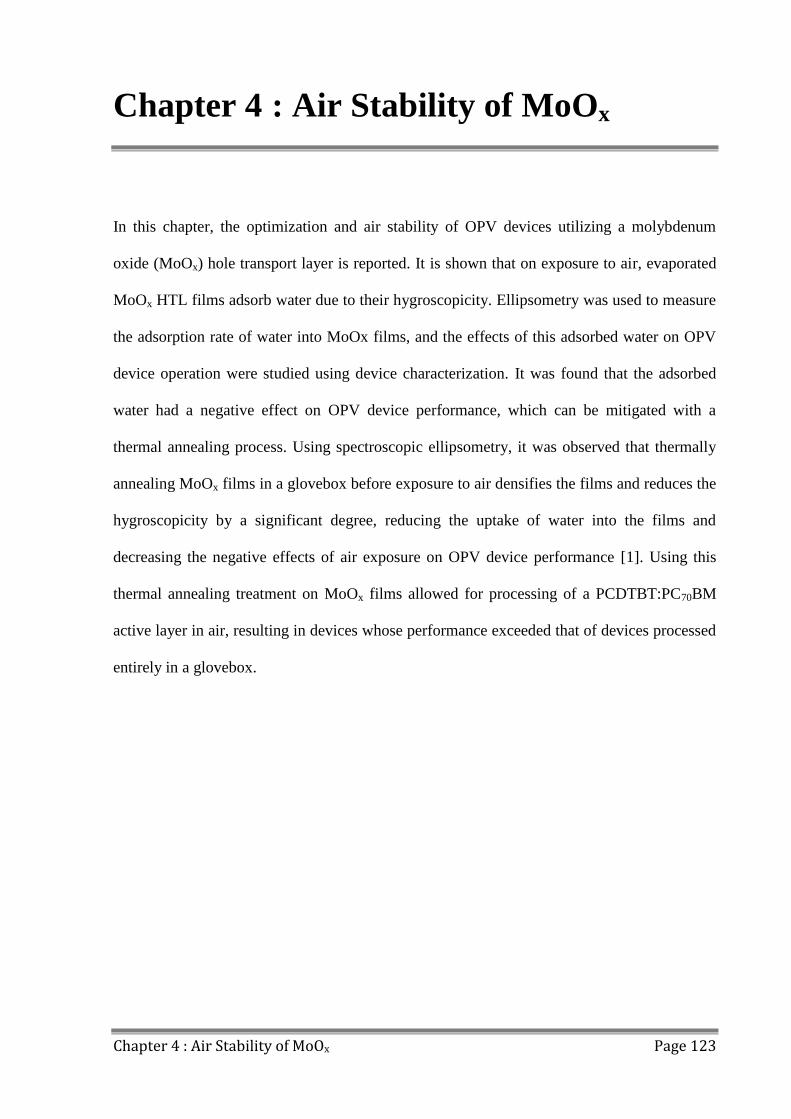
Chapter 4 : Air Stability of MoOx Page 123
Chapter 4 : Air Stability of MoOx
In this chapter, the optimization and air stability of OPV devices utilizing a molybdenum
oxide (MoOx) hole transport layer is reported. It is shown that on exposure to air, evaporated
MoOx HTL films adsorb water due to their hygroscopicity. Ellipsometry was used to measure
the adsorption rate of water into MoOx films, and the effects of this adsorbed water on OPV
device operation were studied using device characterization. It was found that the adsorbed
water had a negative effect on OPV device performance, which can be mitigated with a
thermal annealing process. Using spectroscopic ellipsometry, it was observed that thermally
annealing MoOx films in a glovebox before exposure to air densifies the films and reduces the
hygroscopicity by a significant degree, reducing the uptake of water into the films and
decreasing the negative effects of air exposure on OPV device performance [1]. Using this
thermal annealing treatment on MoOx films allowed for processing of a PCDTBT:PC70BM
active layer in air, resulting in devices whose performance exceeded that of devices processed
entirely in a glovebox.
Chapter 4 : Air Stability of MoOx Page 124
4.0 Introduction
Recent improvements in polymer:fullerene solar cell efficiency and stability have largely
come from the synthesis of new polymers that have lower lying HOMO levels and reduced
energy gap. A lower lying HOMO level has the twin benefit of allowing more of the energy
of each photon to be harvested due to better energy alignment to PCBM [2], while also
improving the stability of the material by making oxidation more difficult. As such, there has
been a recent trend for high efficiency OPVs to utilize polymers with HOMO levels in the
region of -5.1 eV to -5.5 eV, including PTB7 [3] (-5.15 eV) and PCDTBT [4] (-5.5 eV).
These materials contrast with more well-established polymer electron-donors such as P3HT
[5] and MEH-PPV [6] that have HOMO levels of around -5.0 eV.
To utilize these materials with lower lying HOMO levels also requires the use of hole
extraction contacts having a similarly low lying work-function. A variety of such interface
layers have been investigated, including transition metal oxides such as MoOx [5], WOx [7]
and VOx [8]. In particular, MoOx has been studied due to its low lying conduction band onset
(-6.7 eV [9]) and its ease of deposition via thermal evaporation [10], sputtering [11] and
solution processing [12]. When used as the hole transport layer (HTL) in an OPV device
containing an organic semiconductor with a large ionisation potential, the organic
semiconductor close to the MoOx interface has been shown to become p-doped as a result of
charge-transfer [9], with such interfaces supporting efficient hole-extraction [13]. This has
resulted in OPVs utilizing a MoOx HTL and the polymer PCDTBT achieving power
conversion efficiencies of over 7% [14].
Chapter 4 : Air Stability of MoOx Page 125
4.1 MoOx Films and Ambient Conditions
However, whilst MoOx can be utilized to produce high-efficiency OPV devices, it is not
without problems. In particular MoOx is susceptible to loss of oxygen during evaporation
which can result in changes in stoichiometry and electronic energy levels [15]. This is
illustrated in Figure 4.1, where after use in one thermal evaporation the colour of MoOx
source pellets changes from green/yellow to dark grey.
Figure 4.1 Colour change of MoOx source pellets after one evaporation: (a) fresh pellets and
(b) pellets after one thermal evaporation.
In certain states MoOx is also hygroscopic, and can adsorb water to produce a hydrated crystal
within a few Langmuir [16] (defined as an exposure of 10-6
torr in one second). It is believed
that water species adsorbed into the MoOx crystal either reside between the MoOx clusters in
the bulk of the material, changing the cluster size and, as a result, the band gap [9], or are
weakly bound by Van der Walls forces on the surface [17], [18] as either H2O or hydroxide
ions [19]. Water adsorption can occur on timescales of a few tens of minutes even in a highly
pure nitrogen atmosphere with water levels of less than 1 ppm [16], and almost
instantaneously in air. This sensitivity suggests that understanding, and stabilizing, the
oxidation and hydration state of MoOx will be a key requirement for its use in OPV devices.
Chapter 4 : Air Stability of MoOx Page 126
4.2 MoOx Film and Device Preparation
MoOx films were prepared by thermal evaporation, discussed in 3.1.4 Thermal Evaporation.
2 - 4 mm pellets of molybdenum (VI) oxide were purchased from Testbourne Ltd and used as
received. MoOx was deposited via thermal evaporation under a vacuum of < 5E-7 mbar at a
rate of 0.2 Ås-1
using fresh molybdenum (VI) oxide pellets for each evaporation due to the
change of oxidation state of the pellets as shown in Figure 4.1. A series of different films
were prepared; films for OPV devices were deposited onto cleaned ITO coated glass
substrates and had a thickness of 10 nm, whilst films for ellipsometry were deposited onto
silicon wafers, which were cleaned using the same process as the OPV substrates, and had a
thickness between 15 and 20 nm. The cleaning procedure is described in 3.1.1 Substrate
Cleaning.
OPV devices had a standard ITO/MoOx/PCDTBT:PC70BM/Ca/Al architecture, with MoOx
forming the HTL and Ca forming the ETL. The PCDTBT used was the R3CH batch, the
details of which are shown in Table 4.1, and the PC70BM used was 95% pure, the other 5%
being PC60BM. Both materials were sourced from Ossila Ltd. PCDTBT:PC70BM active layers
were deposited by spin-coating, as covered in 3.1.3 Thin Film Deposition, in either the
glovebox under inert atmosphere or in a Lamarflo workstation in air, to a thickness of 70 nm
as measured by a Dektak profilometer. The calcium and aluminium top contact (sourced from
Sigma-Aldrich, 99% and 99.99% purity respectively) was thermally evaporated at a pressure
of < 5*10-7
mbar in the evaporation chamber to a thickness of 2.5 nm and 100 nm
respectively.
In situ spectroscopic ellipsometry was used to study the uptake of moisture and the effects of
thermal annealing on MoOx, the methodology of which is discussed in 3.5 Spectroscopic
Ellipsometry.
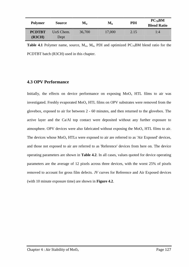
Chapter 4 : Air Stability of MoOx Page 127
Polymer Source Mw Mn PDI PC70BM
Blend Ratio
PCDTBT
(R3CH)
UoS Chem.
Dept
36,700 17,000 2.15 1:4
Table 4.1 Polymer name, source, Mw, Mn, PDI and optimized PC70BM blend ratio for the
PCDTBT batch (R3CH) used in this chapter.
4.3 OPV Performance
Initially, the effects on device performance on exposing MoOx HTL films to air was
investigated. Freshly evaporated MoOx HTL films on OPV substrates were removed from the
glovebox, exposed to air for between 2 - 60 minutes, and then returned to the glovebox. The
active layer and the Ca/Al top contact were deposited without any further exposure to
atmosphere. OPV devices were also fabricated without exposing the MoOx HTL films to air.
The devices whose MoOx HTLs were exposed to air are referred to as 'Air Exposed' devices,
and those not exposed to air are referred to as 'Reference' devices from here on. The device
operating parameters are shown in Table 4.2. In all cases, values quoted for device operating
parameters are the average of 12 pixels across three devices, with the worst 25% of pixels
removed to account for gross film defects. JV curves for Reference and Air Exposed devices
(with 10 minute exposure time) are shown in Figure 4.2.
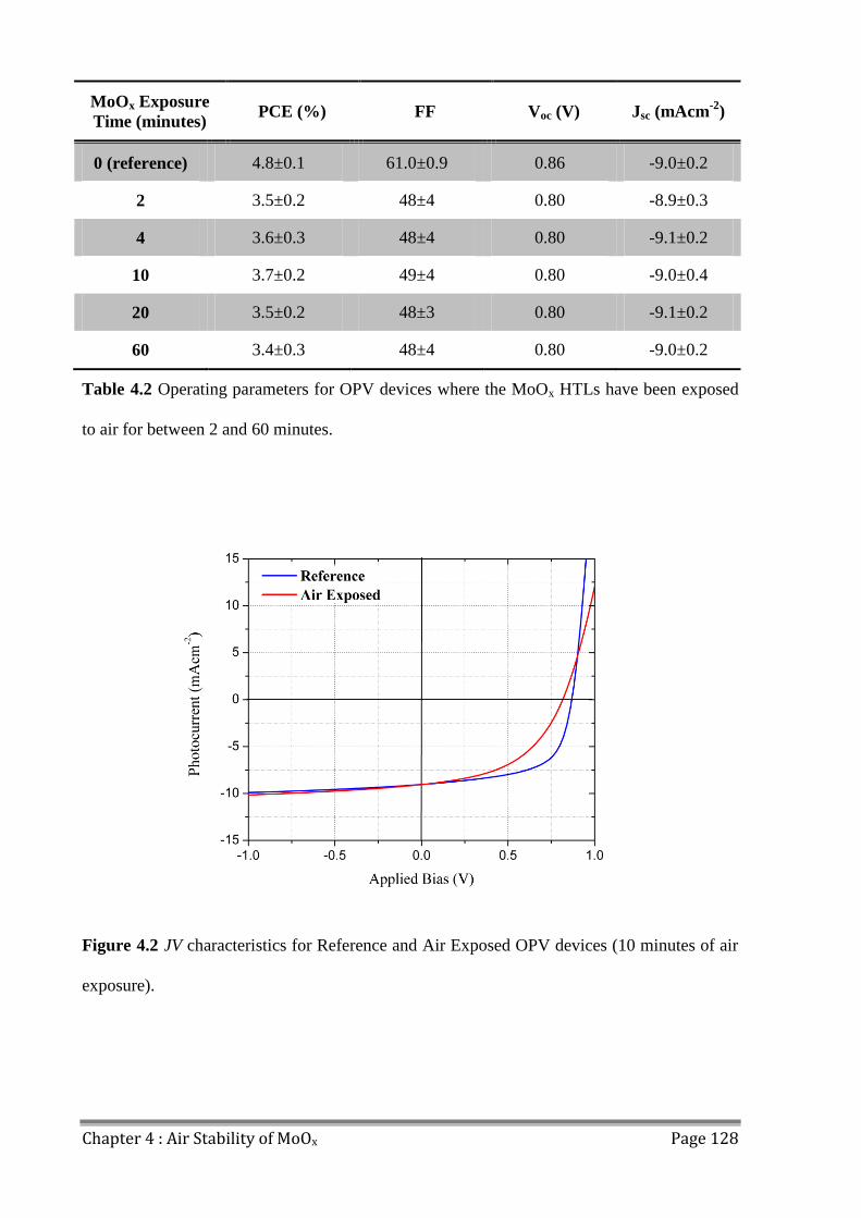
Chapter 4 : Air Stability of MoOx Page 128
MoOx Exposure
Time (minutes) PCE (%) FF Voc (V) Jsc (mAcm
-2)
0 (reference) 4.8±0.1 61.0±0.9 0.86 -9.0±0.2
2 3.5±0.2 48±4 0.80 -8.9±0.3
4 3.6±0.3 48±4 0.80 -9.1±0.2
10 3.7±0.2 49±4 0.80 -9.0±0.4
20 3.5±0.2 48±3 0.80 -9.1±0.2
60 3.4±0.3 48±4 0.80 -9.0±0.2
Table 4.2 Operating parameters for OPV devices where the MoOx HTLs have been exposed
to air for between 2 and 60 minutes.
Figure 4.2 JV characteristics for Reference and Air Exposed OPV devices (10 minutes of air
exposure).
Chapter 4 : Air Stability of MoOx Page 129
It can be seen that exposing MoOx HTLs to air for short periods of time, before active layer
deposition in a glovebox, results in a reduction in device performance due to a loss of Voc and
FF. This reduction in PCE is attributed to adsorption of water into the bulk of the MoOx film
on exposure to air. Previous measurements have shown that MoOx is hygroscopic and that its
work-function is sensitive to exposure to water, and can change by up to 1.2 eV almost
instantaneously on contact with moisture in the atmosphere [16]. Other studies have
concluded that this results from a change in hydration state [9], with X-ray scattering used to
demonstrate the presence of water molecules adsorbed within the MoOx crystal [20]. When
used with PCDTBT, the large electron-affinity of MoOx (-6.7 eV) permits charge-transfer
doping of the PCDTBT around the MoOx-PCDTBT interface. However, the work-function of
the hydrated form of MoOx is lower lying by up to 1.2 eV [16], with such a reduction in
work-function reducing p-type doping and thus resulting in internal charge extraction losses
as confirmed by a reduction in Voc and FF as can be seen in Table 4.2. It can be seen that the
negative effect on device performance does not vary for air exposure times, indicating that the
process of water adsorption is very fast, a result in agreement with previous studies.
To explore whether this reduction in device efficiency as a result of air exposure could be
recovered, thermal annealing was used under an inert atmosphere to attempt to remove
moisture from the film. The approach here is based on previous work in which it has been
shown that thermal annealing at temperatures up to 120C can modify the hydration state of
thin film MoOx, with higher temperatures altering the oxidation state [20]. To test such an
approach, MoOx HTL films were exposed to air for 5 minutes, and on return to the glovebox
were thermally annealed at temperatures between 80 - 150oC for 30 minutes after exposure to
air, with device operating parameters shown in Table 4.3. It should be noted that OPV device
characteristics quoted in Tables 4.2-4.5 represent individual batches of devices fabricated on
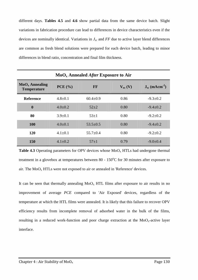
Chapter 4 : Air Stability of MoOx Page 130
different days. Tables 4.5 and 4.6 show partial data from the same device batch. Slight
variations in fabrication procedure can lead to differences in device characteristics even if the
devices are nominally identical. Variations in Jsc and FF due to active layer blend differences
are common as fresh blend solutions were prepared for each device batch, leading to minor
differences in blend ratio, concentration and final film thickness.
MoOx Annealed After Exposure to Air
MoOx Annealing
Temperature PCE (%) FF Voc (V) Jsc (mAcm
-2)
Reference 4.8±0.1 60.4±0.9 0.86 -9.3±0.2
0 4.0±0.2 52±2 0.80 -9.4±0.2
80 3.9±0.1 53±1 0.80 -9.2±0.2
100 4.0±0.1 53.5±0.5 0.80 -9.4±0.2
120 4.1±0.1 55.7±0.4 0.80 -9.2±0.2
150 4.1±0.2 57±1 0.79 -9.0±0.4
Table 4.3 Operating parameters for OPV devices whose MoOx HTLs had undergone thermal
treatment in a glovebox at temperatures between 80 - 150oC for 30 minutes after exposure to
air. The MoOx HTLs were not exposed to air or annealed in 'Reference' devices.
It can be seen that thermally annealing MoOx HTL films after exposure to air results in no
improvement of average PCE compared to 'Air Exposed' devices, regardless of the
temperature at which the HTL films were annealed. It is likely that this failure to recover OPV
efficiency results from incomplete removal of adsorbed water in the bulk of the films,
resulting in a reduced work-function and poor charge extraction at the MoOx-active layer
interface.

Chapter 4 : Air Stability of MoOx Page 131
The effects of applying the same thermal treatment to a MoOx film before it was exposed to
air (referred to as ‘Annealed before Exposure’) was also investigated, with the JV
characteristics of devices shown in Table 4.4.
MoOx Annealed Before Exposure to Air
MoOx Annealing
Temperature PCE (%) FF Voc (V) Jsc (mAcm
-2)
Reference 5.06±0.06 62.7±0.2 0.86 -9.4±0.1
0 4.0±0.1 52±1 0.80 -9.5±0.3
80 4.6±0.2 57±2 0.85 -9.5±0.1
100 4.89±0.07 59.4±0.4 0.86 -9.57±0.06
120 4.89±0.05 59.8±0.3 0.86 -9.51±0.09
150 4.84±0.05 60.6±0.4 0.85 -9.4±0.1
Table 4.4 Operating parameters for OPV devices whose MoOx HTLs had undergone thermal
treatment in a glovebox at temperatures between 80 - 150oC for 30 minutes before exposure to
air for 5 minutes. The MoOx HTLs were not exposed to air or annealed in 'Reference' devices.
Here it can be seen that thermally annealing the MoOx HTL films before exposure to air (for 5
minutes) prevents the significant loss in device efficiency seen in the 'Air Exposed' devices.
The reasons for this are discussed in 4.3 Water Adsorption. For thermal treatments before or
after exposure to air, 100oC or 120
oC for 30 minutes resulted in the best performing devices.
Higher temperatures (150oC) resulted in losses of Voc, likely due to changes in the
stoichiometry of MoOx [20]. 120oC was chosen as the optimal thermal treatment temperature
as it consistently gave the highest performing OPV devices over multiple device batches in
addition to those shown here.
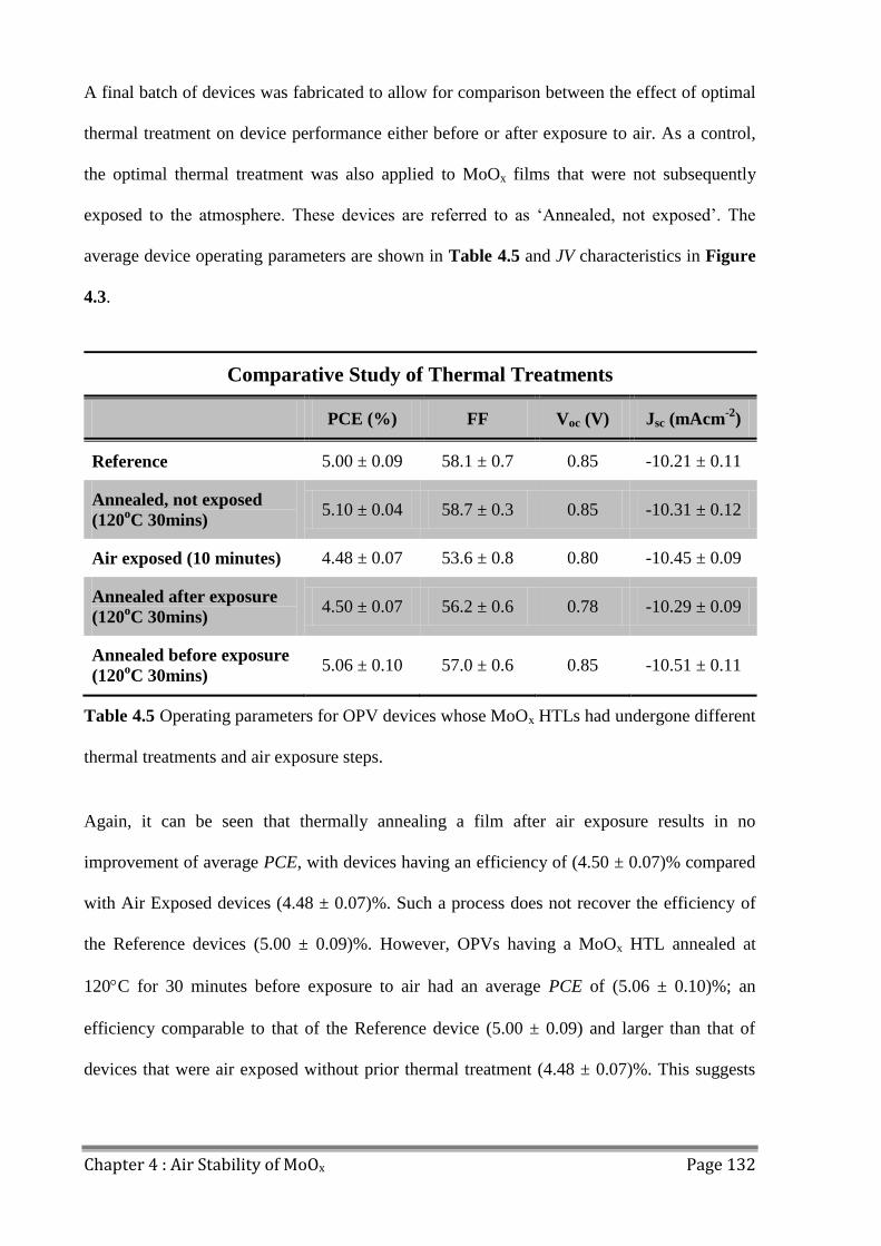
Chapter 4 : Air Stability of MoOx Page 132
A final batch of devices was fabricated to allow for comparison between the effect of optimal
thermal treatment on device performance either before or after exposure to air. As a control,
the optimal thermal treatment was also applied to MoOx films that were not subsequently
exposed to the atmosphere. These devices are referred to as ‘Annealed, not exposed’. The
average device operating parameters are shown in Table 4.5 and JV characteristics in Figure
4.3.
Comparative Study of Thermal Treatments
PCE (%) FF
Voc (V)
Jsc (mAcm-2
)
Reference 5.00 ± 0.09 58.1 ± 0.7 0.85 -10.21 ± 0.11
Annealed, not exposed
(120oC 30mins)
5.10 ± 0.04 58.7 ± 0.3 0.85 -10.31 ± 0.12
Air exposed (10 minutes) 4.48 ± 0.07 53.6 ± 0.8 0.80 -10.45 ± 0.09
Annealed after exposure
(120oC 30mins)
4.50 ± 0.07 56.2 ± 0.6 0.78 -10.29 ± 0.09
Annealed before exposure
(120oC 30mins)
5.06 ± 0.10 57.0 ± 0.6 0.85 -10.51 ± 0.11
Table 4.5 Operating parameters for OPV devices whose MoOx HTLs had undergone different
thermal treatments and air exposure steps.
Again, it can be seen that thermally annealing a film after air exposure results in no
improvement of average PCE, with devices having an efficiency of (4.50 ± 0.07)% compared
with Air Exposed devices (4.48 ± 0.07)%. Such a process does not recover the efficiency of
the Reference devices (5.00 ± 0.09)%. However, OPVs having a MoOx HTL annealed at
120C for 30 minutes before exposure to air had an average PCE of (5.06 ± 0.10)%; an
efficiency comparable to that of the Reference device (5.00 ± 0.09) and larger than that of
devices that were air exposed without prior thermal treatment (4.48 ± 0.07)%. This suggests
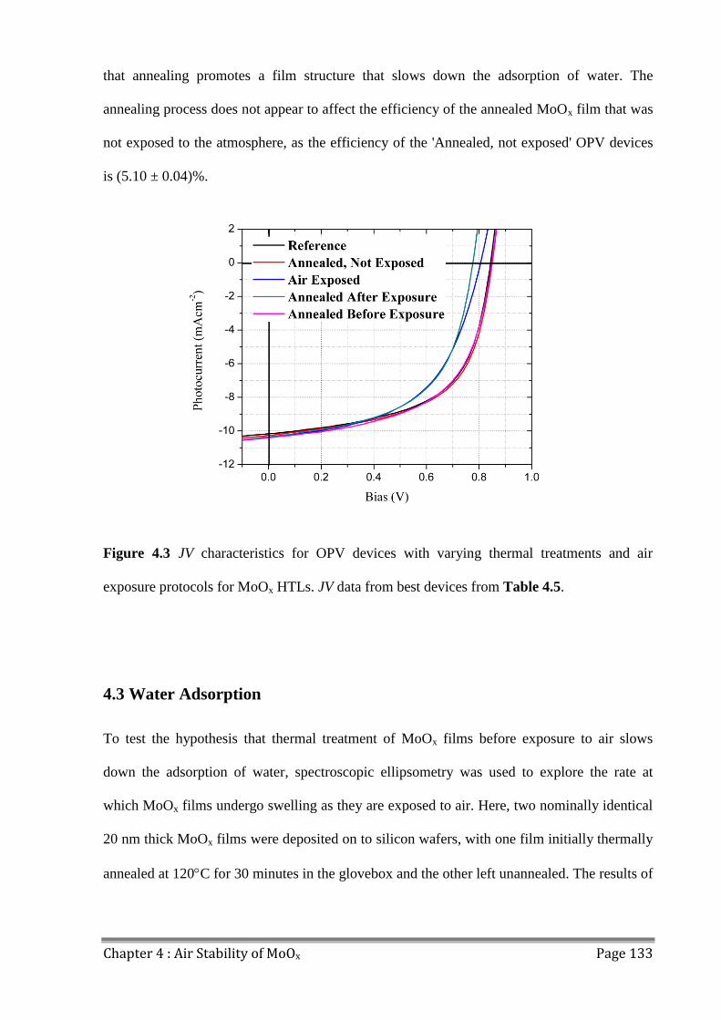
Chapter 4 : Air Stability of MoOx Page 133
that annealing promotes a film structure that slows down the adsorption of water. The
annealing process does not appear to affect the efficiency of the annealed MoOx film that was
not exposed to the atmosphere, as the efficiency of the 'Annealed, not exposed' OPV devices
is (5.10 ± 0.04)%.
Figure 4.3 JV characteristics for OPV devices with varying thermal treatments and air
exposure protocols for MoOx HTLs. JV data from best devices from Table 4.5.
4.3 Water Adsorption
To test the hypothesis that thermal treatment of MoOx films before exposure to air slows
down the adsorption of water, spectroscopic ellipsometry was used to explore the rate at
which MoOx films undergo swelling as they are exposed to air. Here, two nominally identical
20 nm thick MoOx films were deposited on to silicon wafers, with one film initially thermally
annealed at 120C for 30 minutes in the glovebox and the other left unannealed. The results of

Chapter 4 : Air Stability of MoOx Page 134
this experiment are shown in Figure 4.4, where the % change in film thickness as a function
of exposure time is shown. It can be seen that the unannealed MoOx film undergoes an
increase in thickness of around 1.30% over the course of the experiment, while the film that
was initially thermally annealed undergoes a much smaller increase in thickness (around
0.18%). This process has a time constant of 10s of minutes, and is significantly longer that
reported elsewhere on the basis of in-situ XPS data [16]. However the ellipsometry
measurements probe the bulk of the film rather than being sensitive to the properties of the
surface alone, which is likely to undergo much faster changes. The findings demonstrate a
correlation between the uptake of moisture by a MoOx film and reduced device efficiency,
and confirm the speculation that thermal annealing suppresses the uptake of moisture, thereby
resulting in a smaller change in work-function and thus improved device performance.
Figure 4.4 % thickness change over time for annealed and unannealed MoOx films exposed to
air.

Chapter 4 : Air Stability of MoOx Page 135
The thermal annealing process results in a densification of the MoOx film, thereby reducing
its porosity and limiting its ability to adsorb moisture, with such a densification process
resulting from thermal annealing previously observed in other metal-oxide films [17].
Ellipsometry was again used to measure changes in the thickness of a pristine MoOx film as it
was annealed at 120oC for 30 minutes in a nitrogen atmosphere and then returned to room
temperature. The results of which are shown in Figure 4.5. The initial increase in thickness is
due to thermal expansion, but on return to room-temperature the thickness of the MoOx film
was reduced by 0.19%, suggesting an increase in density of the same order. This increase in
film density most likely results from a reduction of the volume of voids between grains in the
MoOx crystal, thereby reducing its ability to adsorb water. This increased density and
reduction in voids between MoOx crystals results in the reduced hygroscopicity of the
thermally annealed MoOx film on exposure to air in Figure 4.4.
Figure 4.5 % film thickness change for a MoOx film thermally annealed for 30 minutes at
120oC in a nitrogen atmosphere before being returned to room temperature.
Chapter 4 : Air Stability of MoOx Page 136
The effects of water adsorption and thermal annealing on MoOx energy levels were studied
with the use of x-ray photoelectron spectroscopy (XPS) and ultra-violet photoelectron
spectroscopy (UPS) techniques. XPS confirmed the presence of O-H (water) bonds within
MoOx films that had been exposed to air, with fewer bonds present in those that had been
thermally annealed. A shift in the MoOx HOMO level between samples was also measured by
UPS. However, due to the nature of the equipment used, there was no opportunity to
measured a pristine sample of MoOx that had not been exposed to air as the samples were
loaded into the equipment in an ambient atmosphere. Therefore, with no reference with which
to compare the results to, no strong conclusions could be drawn, and the results have been left
out of this thesis.
4.4 Air Processing Photoactive Layers
It is possible to use this enhanced stability of MoOx to air exposure on thermal annealing to
explore the processing of the active semiconductor under ambient conditions. OPV devices
were fabricated in which the PCDTBT:PC70BM blend was spin-coated in air under a
Lamarflo workstation before being returned to the glovebox for cathode evaporation and
encapsulation. Here, the active layer was deposited on untreated MoOx films and on MoOx
films that had been thermally annealed in a glove-box at 120C for 30 minutes prior to
exposure to air. Such devices are identified as ‘Air processed’ and ‘Annealed, air processed’.
The JV curves of the devices are shown in Figure 4.6, with device operating parameters
summarized in Table 4.6.
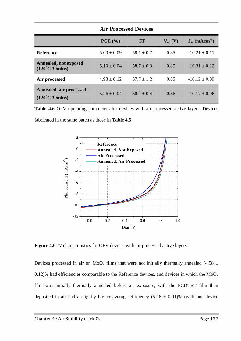
Chapter 4 : Air Stability of MoOx Page 137
Air Processed Devices
PCE (%) FF
Voc (V)
Jsc (mAcm-2
)
Reference 5.00 ± 0.09 58.1 ± 0.7 0.85 -10.21 ± 0.11
Annealed, not exposed
(120oC 30mins)
5.10 ± 0.04 58.7 ± 0.3 0.85 -10.31 ± 0.12
Air processed 4.98 ± 0.12 57.7 ± 1.2 0.85 -10.12 ± 0.09
Annealed, air processed
(120oC 30mins)
5.26 ± 0.04 60.2 ± 0.4 0.86 -10.17 ± 0.06
Table 4.6 OPV operating parameters for devices with air processed active layers. Devices
fabricated in the same batch as those in Table 4.5.
Figure 4.6 JV characteristics for OPV devices with air processed active layers.
Devices processed in air on MoOx films that were not initially thermally annealed (4.98 ±
0.12)% had efficiencies comparable to the Reference devices, and devices in which the MoOx
film was initially thermally annealed before air exposure, with the PCDTBT film then
deposited in air had a slightly higher average efficiency (5.26 ± 0.04)% (with one device
Chapter 4 : Air Stability of MoOx Page 138
having an efficiency of 5.36%) compared to devices that were thermally annealed and then
processed in the glovebox (5.10 ± 0.04)%. This small, but surprising, improvement in
efficiency results from improved Voc and FF, indicating that spin-coating the active layer in
air onto thermally annealed MoOx films is apparently beneficial to charge extraction at the
polymer-MoOx interface.
We speculate that this improvement in device efficiency does not result from changes in the
active organic layer, as no apparent changes are detected in Jsc. Rather, the improvement
derives from the presence of a thin layer of a water species on the surface of the MoOx film.
Such a surface-bound layer is apparently not detrimental to device efficiency (as opposed to
water adsorbed within the MoOx film that reduces the work-function), as it will result in the
formation of a dipole, due to the charged nature of the water species chemically bound to the
surface [18], [21].
This dipole layer may then promote charge extraction, resulting in improved device efficiency
as seen in 'Air Processed' and 'Annealed, Air Processed' devices via an improved Voc and FF.
This improvement is not seen in devices in which the active layer was deposited in the glove
box, as the weakly bound water species on the surface of air exposed MoOx films are likely to
be partially removed in the vacuum load-lock on re-entry to the glovebox. Therefore, the
devices in which the active layer was spun in air show an improvement over devices prepared
in the glovebox as water species are still present on the surface of the MoOx when the active
layer is deposited. It is possible that the active layer 'locks in' the water dipole layer,
preventing its removal on re-entry to the glovebox. In 'Air processed' devices, in which the
active layer was deposited in air on a MoOx film that was not initially annealed, water is still
adsorbed into the bulk of the film, resulting in less efficient devices than the 'Annealed, air
Chapter 4 : Air Stability of MoOx Page 139
processed' devices. However, due to the presence of a water dipole layer between the MoOx
film and the active layer, the device efficiency is still greater than the 'Air exposed' devices.
4.5 Conclusions
In summary, the effects on OPV device performance of exposure of MoOx HTLs to air has
been studied, and thermal treatments to stabilize the MoOx film developed. As MoOx films
are hygroscopic, spectroscopic ellipsometry measurements have shown that air exposure
results in a swelling of the MoOx on adsorption of water that is detrimental to device
efficiency. However by applying an initial thermal anneal to the MoOx film, this uptake of
water can be suppressed; a process that results from film densification. This result is then used
to fabricate OPV devices based on a blend of PCDTBT:PC70BM, with the active
semiconductor layer spin cast in air. Such air-processed devices had an average value for PCE
of (5.26 ± 0.04)%; a value significantly larger than that of devices in which no thermal anneal
process was applied that were fabricated inside a nitrogen-filled glovebox (5.00 ± 0.09)%.
This promising result suggests that the active layers of a polymer photovoltaic device can be
fabricated using an air-based processing route; a result that may be of significant benefit in the
development of a low cost, high volume manufacturing process.
Chapter 4 : Air Stability of MoOx Page 140
4.6 References
[1] E. S. R. Bovill, J. Griffin, T. Wang, J. W. Kingsley, H. Yi, A. Iraqi, A. R. Buckley,
and D. G. Lidzey, “Air processed organic photovoltaic devices incorporating a MoOx anode
buffer layer,” Appl. Phys. Lett., vol. 102, no. 18, p. 183303, May 2013.
[2] M. C. Scharber, D. Mühlbacher, M. Koppe, P. Denk, C. Waldauf, A. J. Heeger, and C.
J. Brabec, “Design Rules for Donors in Bulk-Heterojunction Solar Cells—Towards 10 %
Energy-Conversion Efficiency,” Adv. Mater., vol. 18, no. 6, pp. 789–794, Mar. 2006.
[3] Y. Liang, Z. Xu, J. Xia, S.-T. Tsai, Y. Wu, G. Li, C. Ray, and L. Yu, “For the bright
future-bulk heterojunction polymer solar cells with power conversion efficiency of 7.4%.,”
Adv. Mater., vol. 22, no. 20, pp. E135–8, May 2010.
[4] S. Cho, J. H. Seo, S. H. Park, S. Beaupré, M. Leclerc, and A. J. Heeger, “A thermally
stable semiconducting polymer.,” Adv. Mater., vol. 22, no. 11, pp. 1253–7, Mar. 2010.
[5] C.-Y. Nam, D. Su, and C. T. Black, “High-Performance Air-Processed Polymer-
Fullerene Bulk Heterojunction Solar Cells,” Adv. Funct. Mater., vol. 19, no. 22, pp. 3552–
3559, Nov. 2009.
[6] A. L. Holt, J. M. Leger, and S. A. Carter, “Electrochemical and optical
characterization of p- and n-doped poly[2-methoxy-5-(2-ethylhexyloxy)-1,4-
phenylenevinylene].,” J. Chem. Phys., vol. 123, no. 4, p. 044704, Jul. 2005.
[7] M. Vasilopoulou, L. C. Palilis, D. G. Georgiadou, P. Argitis, S. Kennou, I. Kostis, G.
Papadimitropoulos, Ν. Α. Stathopoulos, A. A. Iliadis, N. Konofaos, D. Davazoglou, and L.
Chapter 4 : Air Stability of MoOx Page 141
Sygellou, “Tungsten oxides as interfacial layers for improved performance in hybrid
optoelectronic devices,” Thin Solid Films, vol. 519, no. 17, pp. 5748–5753, Jun. 2011.
[8] G. Li, C.-W. Chu, V. Shrotriya, J. Huang, and Y. Yang, “Efficient inverted polymer
solar cells,” Appl. Phys. Lett., vol. 88, no. 25, p. 253503, 2006.
[9] M. C. Gwinner, R. D. Pietro, Y. Vaynzof, K. J. Greenberg, P. K. H. Ho, R. H. Friend,
and H. Sirringhaus, “Doping of organic semiconductors using molybdenum trioxide: A
quantitative time-dependent electrical and spectroscopic study,” Adv. Funct. Mater., vol. 21,
no. 8, pp. 1432–1441, Apr. 2011.
[10] N. Miyata, T. Suzuki, and R. Ohyama, “Physical properties of evaporated
molybdenum oxide films,” Thin Solid Films, vol. 281–282, pp. 218–222, Aug. 1996.
[11] C. V. Ramana, V. V. Atuchin, V. G. Kesler, V. A. Kochubey, L. D. Pokrovsky, V.
Shutthanandan, U. Becker, and R. C. Ewing, “Growth and surface characterization of sputter-
deposited molybdenum oxide thin films,” Appl. Surf. Sci., vol. 253, no. 12, pp. 5368–5374,
Apr. 2007.
[12] S. R. Hammond, J. Meyer, N. E. Widjonarko, P. F. Ndione, A. K. Sigdel, A. Garcia,
A. Miedaner, M. T. Lloyd, A. Kahn, D. S. Ginley, J. J. Berry, and D. C. Olson, “Low-
temperature, solution-processed molybdenum oxide hole-collection layer for organic
photovoltaics,” J. Mater. Chem., vol. 22, no. 7, p. 3249, 2012.
[13] J. Meyer, S. Hamwi, M. Kröger, W. Kowalsky, T. Riedl, and A. Kahn, “Transition
metal oxides for organic electronics: energetics, device physics and applications.,” Adv.
Mater., vol. 24, no. 40, pp. 5408–27, Oct. 2012.
Chapter 4 : Air Stability of MoOx Page 142
[14] Y. Sun, C. J. Takacs, S. R. Cowan, J. H. Seo, X. Gong, A. Roy, and A. J. Heeger,
“Efficient, air-stable bulk heterojunction polymer solar cells using MoO x as the anode
interfacial layer,” Adv. Mater., vol. 23, no. 19, pp. 2226–2230, May 2011.
[15] A. Siokou, G. Leftheriotis, S. Papaefthimiou, and P. Yianoulis, “Effect of the tungsten
and molybdenum oxidation states on the thermal coloration of amorphous WO3 and MoO3
films,” Surf. Sci., vol. 482–485, pp. 294–299, Jun. 2001.
[16] I. Irfan, A. James Turinske, Z. Bao, and Y. Gao, “Work function recovery of air
exposed molybdenum oxide thin films,” Appl. Phys. Lett., vol. 101, no. 9, p. 093305, 2012.
[17] T. He and J. Yao, “Photochromism of molybdenum oxide,” J. Photochem. Photobiol.
C Photochem. Rev., vol. 4, no. 2, pp. 125–143, Oct. 2003.
[18] X. Yin, H. Han, and A. Miyamoto, “Structure and adsorption properties of MoO 3 :
insights from periodic density functional calculations,” J. Mol. Model., vol. 5, pp. 207–215,
2001.
[19] K. T. Butler, E. Bovill, R. Crespo-Ortero, D. O. Scanlon, D. Lidzey, and A. Walsh,
“Work function engineering of air processed hole transport layers in organic photovoltaics:
Understanding and controlling oxide surface hydration effects,” 2014.
[20] A. Kuzmin and J. Purans, “Dehydration of the molybdenum trioxide hydrates MoO 3 ·
n H 2 O: in situ x-ray absorption spectroscopy study at the Mo K edge,” J. Phys. Condens.
Matter, vol. 12, no. 9, pp. 1959–1970, Mar. 2000.
[21] R. Steim, F. R. Kogler, and C. J. Brabec, “Interface materials for organic solar cells,”
J. Mater. Chem., vol. 20, no. 13, p. 2499, 2010.

Chapter 5 : Hole Transport Layer Lifetime Study Page 143
Chapter 5 : Hole Transport Layer
Laboratory Lifetime Study
In the previous chapter, details were given regarding the air stability of MoOx and its
suitability as a hole transport layer (HTL) in OPV devices. In this chapter, the fabrication and
optimization of OPV devices utilizing a PCDTBT:PC70BM active layer and three different
HTL materials, MoOx, PEDOT:PSS and vanadium oxide (V2Ox), is presented, with all
devices having initial PCEs in excess of 5%. A detailed lifetime study was then carried out on
the devices for 620 hours in the laboratory lifetime testing system, with JV characterization,
LBIC and ELM used to investigate device degradation and image defects present in the
devices on ageing. It was found that a PEDOT:PSS HTL afforded devices the highest degree
of stability, with T80 lifetimes extrapolated to 14,500 hours (~ 7 years). LBIC and ELM
images clearly show a reduced density of defects in the devices with a PEDOT:PSS HTL
when compared to MoOx and V2Ox on ageing. The lifetime study carried out here in conforms
to the ISOS-L-1 standards as covered in 3.11.1 ISOS Laboratory Weathering Testing.
Chapter 5 : Hole Transport Layer Lifetime Study Page 144
5.0 Introduction
Much work on OPV degradation processes have studied devices based on the material poly(3-
hexylthiophene) (P3HT) [1]–[4], with lifetimes of up to 3 years reported [4]. More recently,
outdoor interlaboratory studies have produced devices based on P3HT having extrapolated
lifetimes in excess of 5 years [5], with laboratory studies demonstrating extrapolated device
lifetimes of up to 10 years in OPVs based on polymer system PCDTBT:PC70BM [4], [6].
To improve OPV stability and lifetime, most work thus far has focused on understanding
degradation processes within the polymer:fullerene active semiconductor layer. However
several studies now report the effect of changing other interlayers in a device [7]–[10],
although this work is almost exclusively based on OPVs based on the polymer (P3HT). The
polymer P3HT has been largely superseded by new generations of low energy-gap donor-
acceptor polymers that have significantly enhanced PCE, in particular the polymer PCDTBT.
Studies on PCDTBT have explored device stability and degradation pathways [4], [9], [11]
and have concluded that polycarbazole polymers have a high degree of photostability [12], as
shown in Chapter 6 : Polymer Air Processing, and can be used to create devices having
extended operational lifetimes [4]. The comparatively high degree of stability afforded by
PCDTBT thus presents an opportunity to test the effect of a variety of different hole transport
layer (HTL) materials and determine their relative role in contributing to device stability. To
this end, OPV devices have been fabricated using a PCDTBT:PC70BM OPV (PCDTBT M137
batch from Ossila Ltd) active layer that utilize a range of different hole-transporting layers
including PEDOT:PSS, MoOx and V2Ox. Device PCE was recorded under simulated solar
radiation over a period of 620 hours, and it was found that a PEDOT:PSS HTL afforded
devices the highest degree of stability, with T80 lifetimes extrapolated to 14,500 hours.
Chapter 5 : Hole Transport Layer Lifetime Study Page 145
5.1 Hole Transport Layer Materials
The devices fabricated for this study were based on the standard device architecture of
ITO/HTL/PCDTBT:PC70BM/Ca/Al, in which the hole transport layer was either composed of
MoOx, PEDOT:PSS or V2Ox. 10 nm MoOx HTL films were prepared as in Chapter 4 : Air
Stability of MoOx and were left unannealed.
5.1.1 PEDOT:PSS
PEDOT:PSS is a material that has been widely explored as a hole-transporting layer as it
combines several characteristics that are desirable for OPV applications, including high
conductivity and good film transparency [13]. When used as an interlayer between ITO and
the active layer of an OPV, PEDOT:PSS aids extraction of charges across the interface and
planarizes the surface of ITO [14], reducing the number of shorts and inhomogeneities formed
at the interface. It also increases the work function of the ITO anode, permitting energy level
matching with the donor polymer in the active layer. Thin films of PEDOT:PSS are however
extremely hygroscopic [15], and post deposition thermal treatments are needed to remove any
remaining water in the films, the effects of which are discussed in more detail in Chapter 6 :
Polymer Air Processing.
The PEDOT:PSS solution used herein (Heraeus Clevios™ P VP AI 4083), had a ratio of 1:6
PEDOT to PSS and was filtered through a 0.45 µm PVDF filter to remove any aggregates
before use. To fabricate PEDOT:PSS HTLs, the PEDOT:PSS solution was spin-coated onto
cleaned ITO coated substrates at 6000 rpm for 30 s in air to form a ~ 30 nm thick film, and
then annealed on a hot plate in air for 10 minutes at 150C, following which they were
transferred to the glovebox.
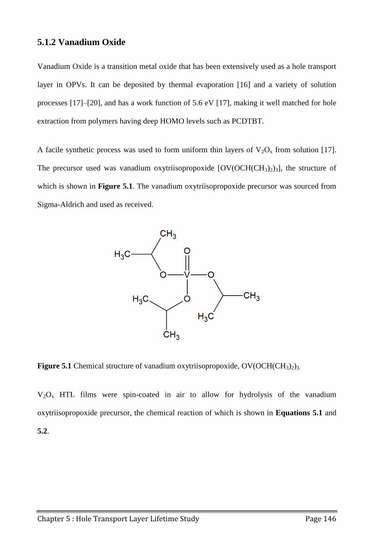
Chapter 5 : Hole Transport Layer Lifetime Study Page 146
5.1.2 Vanadium Oxide
Vanadium Oxide is a transition metal oxide that has been extensively used as a hole transport
layer in OPVs. It can be deposited by thermal evaporation [16] and a variety of solution
processes [17]–[20], and has a work function of 5.6 eV [17], making it well matched for hole
extraction from polymers having deep HOMO levels such as PCDTBT.
A facile synthetic process was used to form uniform thin layers of V2Ox from solution [17].
The precursor used was vanadium oxytriisopropoxide [OV(OCH(CH3)2)3], the structure of
which is shown in Figure 5.1. The vanadium oxytriisopropoxide precursor was sourced from
Sigma-Aldrich and used as received.
Figure 5.1 Chemical structure of vanadium oxytriisopropoxide, OV(OCH(CH3)2)3.
V2Ox HTL films were spin-coated in air to allow for hydrolysis of the vanadium
oxytriisopropoxide precursor, the chemical reaction of which is shown in Equations 5.1 and
5.2.
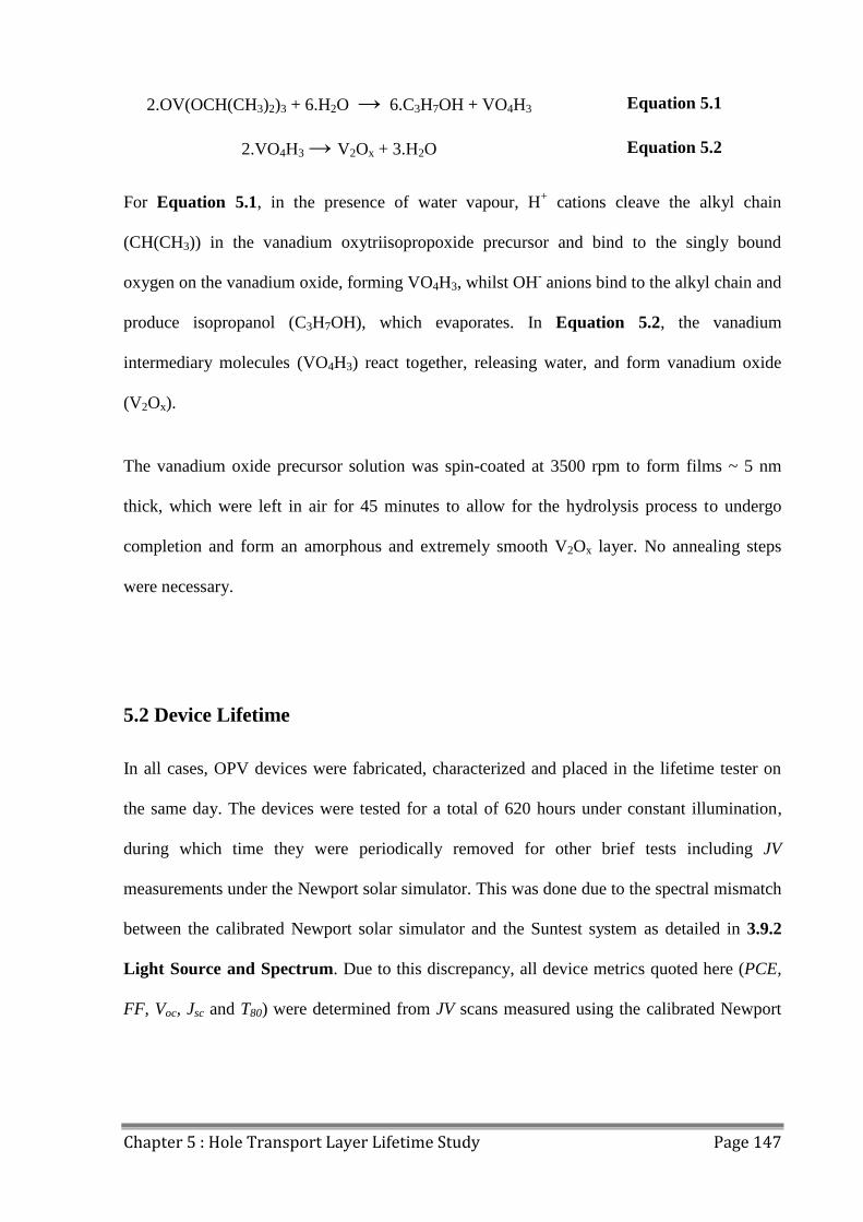
Chapter 5 : Hole Transport Layer Lifetime Study Page 147
2.OV(OCH(CH3)2)3 + 6.H2O → 6.C3H7OH + VO4H3 Equation 5.1
2.VO4H3 → V2Ox + 3.H2O Equation 5.2
For Equation 5.1, in the presence of water vapour, H+ cations cleave the alkyl chain
(CH(CH3)) in the vanadium oxytriisopropoxide precursor and bind to the singly bound
oxygen on the vanadium oxide, forming VO4H3, whilst OH- anions bind to the alkyl chain and
produce isopropanol (C3H7OH), which evaporates. In Equation 5.2, the vanadium
intermediary molecules (VO4H3) react together, releasing water, and form vanadium oxide
(V2Ox).
The vanadium oxide precursor solution was spin-coated at 3500 rpm to form films ~ 5 nm
thick, which were left in air for 45 minutes to allow for the hydrolysis process to undergo
completion and form an amorphous and extremely smooth V2Ox layer. No annealing steps
were necessary.
5.2 Device Lifetime
In all cases, OPV devices were fabricated, characterized and placed in the lifetime tester on
the same day. The devices were tested for a total of 620 hours under constant illumination,
during which time they were periodically removed for other brief tests including JV
measurements under the Newport solar simulator. This was done due to the spectral mismatch
between the calibrated Newport solar simulator and the Suntest system as detailed in 3.9.2
Light Source and Spectrum. Due to this discrepancy, all device metrics quoted here (PCE,
FF, Voc, Jsc and T80) were determined from JV scans measured using the calibrated Newport
Chapter 5 : Hole Transport Layer Lifetime Study Page 148
solar simulator, with data recorded using the ATLAS is included to highlight general trends in
device metrics as they undergo aging.
The light intensity and temperature inside the test chamber, as measured by the photodiodes
and temperature sensors on the test board, are shown in Figure 5.2. It can be seen that the
light intensity was extremely stable over the course of the experiment. However, the
temperature fluctuated in a regular pattern that followed the room's occupancy during a
working week as a result of the building's heating and air-conditioning systems. At the
weekend, when the room was not in use, the temperature readings were steady (for example,
at the beginning of the test). This led to an daily increase in the temperature inside the test
chamber of ~ 3oC. Regardless of this, the measured values for light intensity and temperature
stayed within accepted variance as stipulated by the ISOS-L-1 test protocol for the duration of
the test.
Figure 5.2 Mean values for temperature and light intensity as measured by the temperature
sensors and photodiodes on the lifetime test board. Error bars represent standard deviation
around the mean.

Chapter 5 : Hole Transport Layer Lifetime Study Page 149
In Figure 5.3, the average values of PCE, FF, Voc and Jsc, determined from the different
devices are shown as a function of irradiation time in the Suntest chamber. Here, data is
normalized to their initial values, with the data shown representing the average values for the
pixels determined every 10 minutes. Jsc and PCE are corrected to account for intensity
fluctuations in the Suntest xenon lamp, which varied by less than ± 5% over the course of the
experiment.
Figure 5.3 shows PCE, Voc, Jsc and FF for devices utilising the different HTL materials as a
function of irradiation time under the ATLAS solar simulator. All data is normalised to its
initial value determined at t = 0. In each part, data is plotted as measured every 10 minutes
using the ATLAS solar simulator (solid lines) and every 3 days using the calibrated Newport
solar simulator (circular data points). The decay in PCE (determined using both types of solar
simulator) is fitted to a straight line (dashed line or dotted line) for times beyond the burn-in
period (t > 250 hours). This linear fit to the PCE is used to determine the T80 decay lifetime.
Chapter 5 : Hole Transport Layer Lifetime Study Page 150
All devices undergo a burn in phase that lasts for ~ 250 hours, in which the FF and Jsc
decrease at an exponential rate, after which the decay follows a linear trend. In Table 5.1 the
average values of PCE, peak EQE, FF, Voc and Jsc (and their uncertainties) are shown for all
devices before and after lifetime testing with corresponding JV and EQE curves shown in
Figure 5.4 and Figure 5.5 respectively. A linear-fit to the PCE data (after the burn-in period)
was used to determine the T80 lifetime of the devices using the data from the ATLAS and
Newport solar simulators (plotted using coloured dashed lines).
The initial burn-in that is observed in all devices (see Figure 5.3) is believed to originate from
photochemical reactions in the PCDTBT:PC70BM blend that adversely affect its charge
transport properties [4], [9], [11], [21]. The EQE spectra recorded before and after irradiation
(see Figure 5.5 (a) and (b) respectively), indicate a general reduction in quantum efficiency
without any change in spectral shape; a result consistent with a degree of photooxidation (note
that there is a systematic error in EQE measurement of ~ 10% but results agree with Jsc within
experimental error). Here, photochemical reactions in PCDTBT result in an increase in the
density of sub-bandgap and trap states that lead to a reduction in hole mobility [9]. Other
work has demonstrated that the inclusion of PCBM in the blend film slows down the rate of
photo-oxidation by quenching the excited state, however oxidation of the fullerene itself can
lead to a reduction in carrier mobility by inducing deep trap states inside the PCBM domains
[21]. The formation of trap states saturates over time, which results in an end to the burn-in
phase and subsequent linear decay [9].
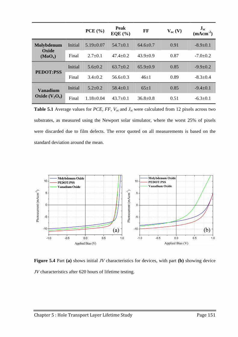
Chapter 5 : Hole Transport Layer Lifetime Study Page 151
PCE (%) Peak
EQE (%) FF Voc (V)
Jsc
(mAcm-2
)
Molybdenum
Oxide
(MoOx)
Initial 5.19±0.07 54.7±0.1 64.6±0.7 0.91 -8.9±0.1
Final 2.7±0.1 47.4±0.2 43.9±0.9 0.87 -7.0±0.2
PEDOT:PSS Initial 5.6±0.2 63.7±0.2 65.9±0.9 0.85 -9.9±0.2
Final 3.4±0.2 56.6±0.3 46±1 0.89 -8.3±0.4
Vanadium
Oxide (V2Ox)
Initial 5.2±0.2 58.4±0.1 65±1 0.85 -9.4±0.1
Final 1.18±0.04 43.7±0.1 36.8±0.8 0.51 -6.3±0.1
Table 5.1 Average values for PCE, FF, Voc and Jsc were calculated from 12 pixels across two
substrates, as measured using the Newport solar simulator, where the worst 25% of pixels
were discarded due to film defects. The error quoted on all measurements is based on the
standard deviation around the mean.
Figure 5.4 Part (a) shows initial JV characteristics for devices, with part (b) showing device
JV characteristics after 620 hours of lifetime testing.
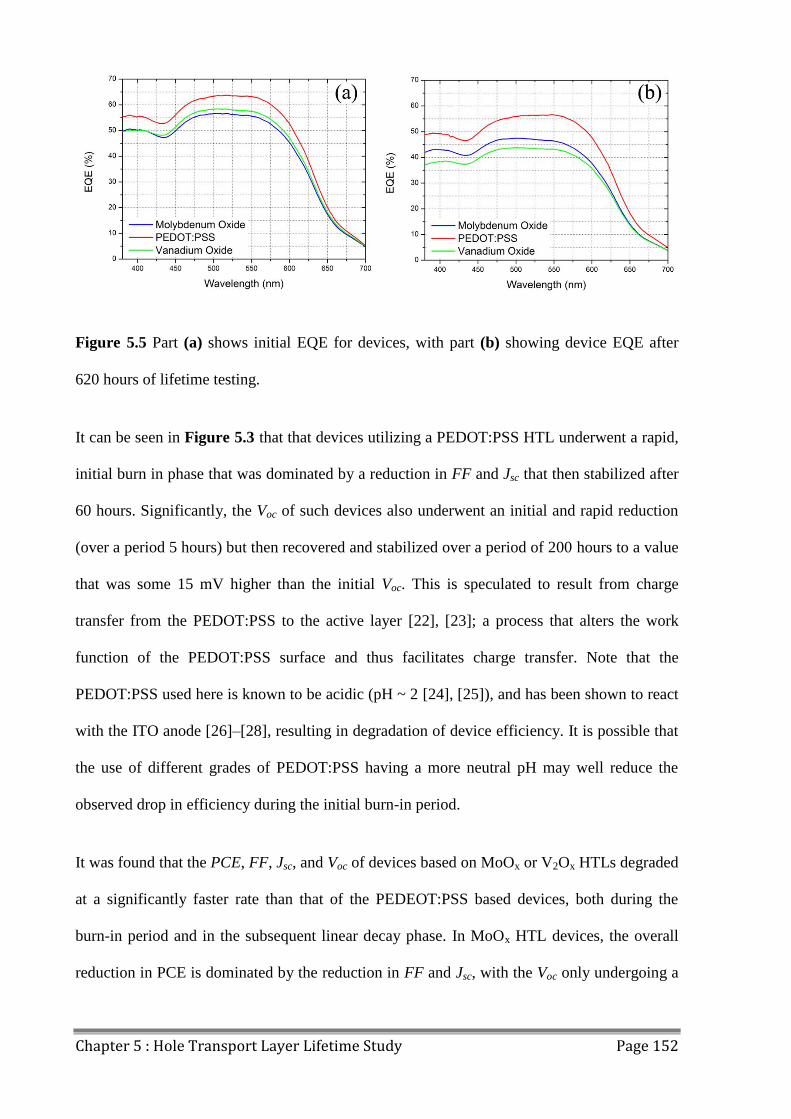
Chapter 5 : Hole Transport Layer Lifetime Study Page 152
Figure 5.5 Part (a) shows initial EQE for devices, with part (b) showing device EQE after
620 hours of lifetime testing.
It can be seen in Figure 5.3 that that devices utilizing a PEDOT:PSS HTL underwent a rapid,
initial burn in phase that was dominated by a reduction in FF and Jsc that then stabilized after
60 hours. Significantly, the Voc of such devices also underwent an initial and rapid reduction
(over a period 5 hours) but then recovered and stabilized over a period of 200 hours to a value
that was some 15 mV higher than the initial Voc. This is speculated to result from charge
transfer from the PEDOT:PSS to the active layer [22], [23]; a process that alters the work
function of the PEDOT:PSS surface and thus facilitates charge transfer. Note that the
PEDOT:PSS used here is known to be acidic (pH ~ 2 [24], [25]), and has been shown to react
with the ITO anode [26]–[28], resulting in degradation of device efficiency. It is possible that
the use of different grades of PEDOT:PSS having a more neutral pH may well reduce the
observed drop in efficiency during the initial burn-in period.
It was found that the PCE, FF, Jsc, and Voc of devices based on MoOx or V2Ox HTLs degraded
at a significantly faster rate than that of the PEDEOT:PSS based devices, both during the
burn-in period and in the subsequent linear decay phase. In MoOx HTL devices, the overall
reduction in PCE is dominated by the reduction in FF and Jsc, with the Voc only undergoing a
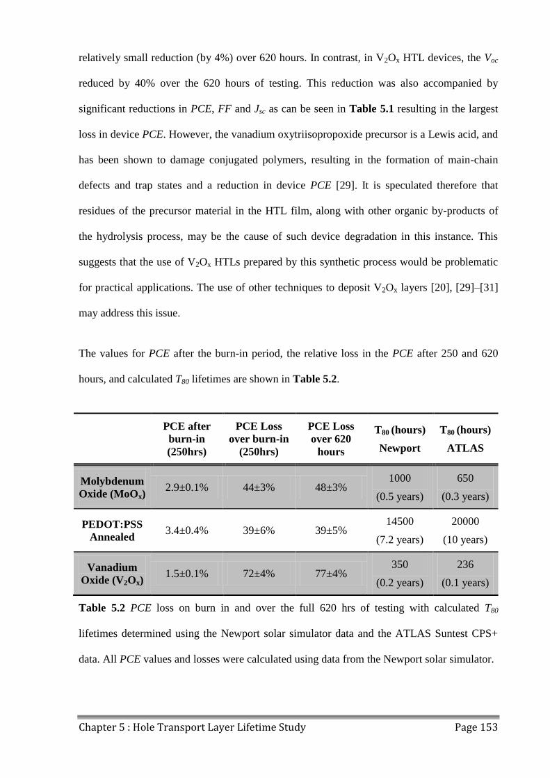
Chapter 5 : Hole Transport Layer Lifetime Study Page 153
relatively small reduction (by 4%) over 620 hours. In contrast, in V2Ox HTL devices, the Voc
reduced by 40% over the 620 hours of testing. This reduction was also accompanied by
significant reductions in PCE, FF and Jsc as can be seen in Table 5.1 resulting in the largest
loss in device PCE. However, the vanadium oxytriisopropoxide precursor is a Lewis acid, and
has been shown to damage conjugated polymers, resulting in the formation of main-chain
defects and trap states and a reduction in device PCE [29]. It is speculated therefore that
residues of the precursor material in the HTL film, along with other organic by-products of
the hydrolysis process, may be the cause of such device degradation in this instance. This
suggests that the use of V2Ox HTLs prepared by this synthetic process would be problematic
for practical applications. The use of other techniques to deposit V2Ox layers [20], [29]–[31]
may address this issue.
The values for PCE after the burn-in period, the relative loss in the PCE after 250 and 620
hours, and calculated T80 lifetimes are shown in Table 5.2.
PCE after
burn-in
(250hrs)
PCE Loss
over burn-in
(250hrs)
PCE Loss
over 620
hours
T80 (hours)
Newport
T80 (hours)
ATLAS
Molybdenum
Oxide (MoOx) 2.9±0.1% 44±3% 48±3%
1000
(0.5 years)
650
(0.3 years)
PEDOT:PSS
Annealed 3.4±0.4% 39±6% 39±5%
14500
(7.2 years)
20000
(10 years)
Vanadium
Oxide (V2Ox) 1.5±0.1% 72±4% 77±4%
350
(0.2 years)
236
(0.1 years)
Table 5.2 PCE loss on burn in and over the full 620 hrs of testing with calculated T80
lifetimes determined using the Newport solar simulator data and the ATLAS Suntest CPS+
data. All PCE values and losses were calculated using data from the Newport solar simulator.
Chapter 5 : Hole Transport Layer Lifetime Study Page 154
The average lifetime for devices using a PEDOT:PSS HTL was calculated to be 14,500 hours
from data acquired from the Newport solar simulator. If other possible catastrophic device
degradation processes are eliminated (e.g. sudden failure of the device encapsulation), the
recorded lifetime is equivalent to 7.2 years of practical operation, assuming an operational
device would receive 5.5 hours of 1000Wm-2
irradiation per day [4]. For MoOx, however the
device T80 lifetime was found to be 1000 hours (equivalent to 6 months operation); a value
reduced to 350 hours (63 days) for the V2Ox HTL devices. It is important to emphasise that
lifetime figures that have been determined here are for devices aged indoors under the ISOS-
L-1 specification [32], as outdoor testing results in thermal cycling and light intensity
variations, as discussed in more detail in Chapter 7 : Outdoor Lifetime Testing.
T80 lifetimes as calculated from data acquired from the ATLAS system are different from
those as calculated using data from the Newport solar simulator, due to the spectral mismatch
of the two light sources and its effect on measured device operating parameters. However, in
all cases the lifetimes as calculated from the different light sources are of a similar magnitude.
It is clear, therefore, that the rate of degradation of all device metrics is a significant function
of the nature of the HTL materials; a result that suggests that degradation in the active layer
cannot completely account for the observed degradation of device performance. Rather, the
changes in FF, Jsc, and Voc that are observed during both burn-in and subsequent linear decay
must also result from the formation of additional trap states at the interface between the active
layer and the hole transport layers, due to generation of structural and compositional defects
[11]. Additional processes are likely to be also active at the interface between the active layer
and the device cathode however the relative importance of such a process cannot be
determined from these experiments.
Chapter 5 : Hole Transport Layer Lifetime Study Page 155
In contrast to previous work [7], [8], [10], the PEDOT:PSS HTL affords devices the highest
stability. This is believed to be mainly due to the use of PCDTBT as opposed to P3HT as the
donor polymer in the devices, though the use of encapsulation also plays a role. PCDTBT has
been shown to be stable in the presence of water and oxygen even under elevated
temperatures [9], which PEDOT:PSS, which is known to be highly hygroscopic [33], tends to
introduce into devices during processing, whereas P3HT is highly sensitive to such ingress
[7], [34]. Other studies have also shown that devices based on PCDTBT:PC70BM using a
PEDOT:PSS hole transport layer have achieved similar device lifetimes [4], though with no
comparison to other hole transport layer materials. The cause of device degradation in devices
utilising the different hole transport layers will require further investigation.
5.3 LBIC/ELM of Aged Devices
After testing in the laboratory lifetime setup for 620 hours, both LBIC and ELM images were
taken of several pixels of the devices, as shown in Figure 5.6. The methods by which the
images were acquired are described in 3.7 Laser Beam Induced Current Mapping (LBIC)
and 3.8 Electroluminescence Mapping (ELM). It was not possible to also obtain these
images prior to testing due to time restrictions, and as such the formation of defects on ageing
devices cannot be studied. However, the density of defects shown in the LBIC and ELM
images can be compared between device types.
For LBIC images, the colour scale is shown in Figure 5.6, with high generated current
indicated by dark blue, and low current indicated by red. ELM images are shown in greyscale,
with lighter areas indicating higher electroluminescence and black areas indicating little or no
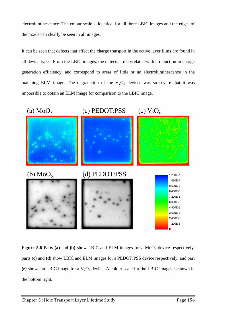
Chapter 5 : Hole Transport Layer Lifetime Study Page 156
electroluminescence. The colour scale is identical for all three LBIC images and the edges of
the pixels can clearly be seen in all images.
It can be seen that defects that affect the charge transport in the active layer films are found in
all device types. From the LBIC images, the defects are correlated with a reduction in charge
generation efficiency, and correspond to areas of little or no electroluminescence in the
matching ELM image. The degradation of the V2Ox devices was so severe that it was
impossible to obtain an ELM image for comparison to the LBIC image.
Figure 5.6 Parts (a) and (b) show LBIC and ELM images for a MoOx device respectively,
parts (c) and (d) show LBIC and ELM images for a PEDOT:PSS device respectively, and part
(e) shows an LBIC image for a V2Ox device. A colour scale for the LBIC images is shown in
the bottom right.
Chapter 5 : Hole Transport Layer Lifetime Study Page 157
From previous studies, it has been shown that V2Ox layers formed from an oxytriisopropoxide
precursor and hydrolysis process contain a large number of nano-scopic voids in the film as a
result of solvent evaporation during film formation [17]. These voids in the film, along with
the residual precursor or other organic products of hydrolysation, appear to lead to extensive
defect formation in the active layer of the device, as can be seen in the LBIC images in
Figure 5.6 (e). These defects lead to a drastic reduction in charge generation in the film
around the defect sites. The LBIC image for the V2Ox device also shows that the charge
generation in the bulk of the film has decreased significantly when compared to the other
HTL devices, which correlates with the relatively large loss in Jsc on ageing as seen in Figure
5.3.
The devices with a MoOx HTL also showed a significant number of defects with a large area
of effect, as can be seen in Figure 5.6 (a,b). It is suspected that these originate from structural
defects in the evaporated MoOx film acting as formation sites for charge trap states and
photochemical reactions in the active layer.
LBIC and ELM measurements also reveal defects in the PEDOT:PSS devices, as seen in
Figure 5.6 (c,d), but in comparison to the other device types they are fewer in number. This,
in combination with the degradation characteristics seen in Figure 5.3, indicate that the
interface between the PEDOT:PSS and the active layer is more stable than MoOx and V2Ox.
Chapter 5 : Hole Transport Layer Lifetime Study Page 158
5.4 Conclusions
These experiments demonstrate that the rate of degradation of the device metrics is a
significant function of the nature of the HTL material; a result that confirms that degradation
in the active layer does not completely account for the observed reduction in device
performance. Rather, the changes in FF, Jsc, and Voc that are observed during both burn-in and
subsequent linear decay must also result from the formation of additional trap states at the
interface between the active layer and the hole transport layers, due to generation of structural
and electronic defects [11], as shown in both LBIC and ELM images of the devices after
ageing.
It has been shown that OPV devices utilising a PEDOT:PSS HTL have a higher stability than
comparable devices using a MoOx or V2Ox HTLs, with extrapolated T80 lifetimes for devices
utilising a PEDOT:PSS HTL being 14,500 hours. Such lifetimes are in good accord with the
results of previous studies [4]. Other work [7], [8], [10] however has suggested that OPVs
having a PEDOT:PSS HTLs have relatively poor operational stability. However, this apparent
contradiction likely results from the differing sensitivity of the donor-polymer to trapped
moisture, as previous studies explored OPVs based on the polymer P3HT; a material known
to be sensitive to the presence of moisture that is likely introduced into the device by the
highly hygroscopic PEDOT:PSS [33]. In contrast, however, PCDTBT is more stable to the
presence of water and oxygen even under elevated temperatures [9], and thus the effect of
trapped moisture within the PEDOT:PSS appears less problematic, an effect covered in more
detail in Chapter 6 : Polymer Air Processing.

Chapter 5 : Hole Transport Layer Lifetime Study Page 159
5.5 References
[1] R. De Bettignies, J. Leroy, M. Firon, and C. Sentein, “Accelerated lifetime
measurements of P3HT:PCBM solar cells,” Synth. Met., vol. 156, no. 7–8, pp. 510–513, Apr.
2006.
[2] J. A. Hauch, P. Schilinsky, S. A. Choulis, R. Childers, M. Biele, and C. J. Brabec,
“Flexible organic P3HT:PCBM bulk-heterojunction modules with more than 1 year outdoor
lifetime,” Sol. Energy Mater. Sol. Cells, vol. 92, no. 7, pp. 727–731, Jul. 2008.
[3] M. O. Reese, A. J. Morfa, M. S. White, N. Kopidakis, S. E. Shaheen, G. Rumbles, and
D. S. Ginley, “Pathways for the degradation of organic photovoltaic P3HT:PCBM based
devices,” Sol. Energy Mater. Sol. Cells, vol. 92, no. 7, pp. 746–752, Jul. 2008.
[4] C. H. Peters, I. T. Sachs-Quintana, J. P. Kastrop, S. Beaupré, M. Leclerc, and M. D.
McGehee, “High Efficiency Polymer Solar Cells with Long Operating Lifetimes,” Adv.
Energy Mater., vol. 1, no. 4, pp. 491–494, Jul. 2011.
[5] S. A. Gevorgyan, M. V. Madsen, H. F. Dam, M. Jørgensen, C. J. Fell, K. F. Anderson,
B. C. Duck, A. Mescheloff, E. A. Katz, A. Elschner, R. Roesch, H. Hoppe, M. Hermenau, M.
Riede, and F. C. Krebs, “Interlaboratory outdoor stability studies of flexible roll-to-roll coated
organic photovoltaic modules: Stability over 10,000h,” Sol. Energy Mater. Sol. Cells, vol.
116, pp. 187–196, Sep. 2013.
[6] H. Cao, W. He, Y. Mao, X. Lin, K. Ishikawa, J. H. Dickerson, and W. P. Hess,
“Recent progress in degradation and stabilization of organic solar cells,” J. Power Sources,
vol. 264, pp. 168–183, Oct. 2014.
Chapter 5 : Hole Transport Layer Lifetime Study Page 160
[7] E. Voroshazi, B. Verreet, A. Buri, R. Müller, D. Di Nuzzo, and P. Heremans,
“Influence of cathode oxidation via the hole extraction layer in polymer:fullerene solar cells,”
Org. Electron., vol. 12, no. 5, pp. 736–744, May 2011.
[8] C. Girotto, E. Voroshazi, D. Cheyns, P. Heremans, and B. P. Rand, “Solution-
processed MoO₃ thin films as a hole-injection layer for organic solar cells.,” ACS Appl.
Mater. interfaces, vol. 3, no. 9, pp. 3244–7, 2011.
[9] C. H. Peters, I. T. Sachs-Quintana, W. R. Mateker, T. Heumueller, J. Rivnay, R.
Noriega, Z. M. Beiley, E. T. Hoke, A. Salleo, and M. D. McGehee, “The mechanism of burn-
in loss in a high efficiency polymer solar cell,” Adv. Mater., vol. 24, no. 5, pp. 663–668, Feb.
2012.
[10] Y. Sun, C. J. Takacs, S. R. Cowan, J. H. Seo, X. Gong, A. Roy, and A. J. Heeger,
“Efficient, air-stable bulk heterojunction polymer solar cells using MoO x as the anode
interfacial layer,” Adv. Mater., vol. 23, no. 19, pp. 2226–2230, May 2011.
[11] E. Voroshazi, I. Cardinaletti, T. Conard, and B. P. Rand, “Light-Induced Degradation
of Polymer:Fullerene Photovoltaic Devices: An Intrinsic or Material-Dependent Failure
Mechanism?,” Adv. Energy Mater., Aug. 2014.
[12] E. Bovill, H. Yi, A. Iraqi, and D. G. Lidzey, “The fabrication of polyfluorene and
polycarbazole-based photovoltaic devices using an air-stable process route,” Appl. Phys. Lett.,
vol. 105, no. 22, p. 223302, Dec. 2014.
[13] Q. Wei, M. Mukaida, Y. Naitoh, and T. Ishida, “Morphological change and mobility
enhancement in PEDOT:PSS by adding co-solvents.,” Adv. Mater., vol. 25, no. 20, pp. 2831–
6, May 2013.
Chapter 5 : Hole Transport Layer Lifetime Study Page 161
[14] C. Jonda, A. B. R. Mayer, U. Stolz, A. Elschner, and A. Karbach, “Surface roughness
effects and their influence on the degradation of organic light emitting devices,” J. Mater.
Sci., vol. 35, no. 22, pp. 5645–5651, 2000.
[15] J. Huang, P. F. Miller, J. S. Wilson, A. J. de Mello, J. C. de Mello, and D. D. C.
Bradley, “Investigation of the Effects of Doping and Post-Deposition Treatments on the
Conductivity, Morphology, and Work Function of Poly(3,4-
ethylenedioxythiophene)/Poly(styrene sulfonate) Films,” Adv. Funct. Mater., vol. 15, no. 2,
pp. 290–296, Feb. 2005.
[16] I. Hancox, L. a. Rochford, D. Clare, P. Sullivan, and T. S. Jones, “Utilizing n-type
vanadium oxide films as hole-extracting layers for small molecule organic photovoltaics,”
Appl. Phys. Lett., vol. 99, no. 1, p. 013304, 2011.
[17] K. Zilberberg, S. Trost, H. Schmidt, and T. Riedl, “Solution Processed Vanadium
Pentoxide as Charge Extraction Layer for Organic Solar Cells,” Adv. Energy Mater., vol. 1,
no. 3, pp. 377–381, May 2011.
[18] Y.-M. Chang and J.-M. Ding, “High efficiency inverted polymer solar cells with the
sol–gel derived vanadium oxide interlayer,” Thin Solid Films, vol. 520, no. 16, pp. 5400–
5404, Jun. 2012.
[19] G. Terán-Escobar, J. Pampel, J. M. Caicedo, and M. Lira-Cantú, “Low-temperature,
solution-processed, layered V2O5 hydrate as the hole-transport layer for stable organic solar
cells,” Energy Environ. Sci., vol. 6, no. 10, p. 3088, 2013.
[20] Z. Tan, W. Zhang, C. Cui, Y. Ding, D. Qian, Q. Xu, L. Li, S. Li, and Y. Li, “Solution-
processed vanadium oxide as a hole collection layer on an ITO electrode for high-

Chapter 5 : Hole Transport Layer Lifetime Study Page 162
performance polymer solar cells.,” Phys. Chem. Chem. Phys., vol. 14, no. 42, pp. 14589–95,
Nov. 2012.
[21] M. O. Reese, A. M. Nardes, B. L. Rupert, R. E. Larsen, D. C. Olson, M. T. Lloyd, S.
E. Shaheen, D. S. Ginley, G. Rumbles, and N. Kopidakis, “Photoinduced Degradation of
Polymer and Polymer-Fullerene Active Layers: Experiment and Theory,” Adv. Funct. Mater.,
vol. 20, no. 20, pp. 3476–3483, Oct. 2010.
[22] C. Perlov, W. Jackson, C. Taussig, S. Mo, and S. R. Forrest, “A polymer /
semiconductor write-once read-many-times memory,” vol. 426, no. November, pp. 2–5, 2003.
[23] R. A. Nawrocki, E. M. Galiger, D. P. Ostrowski, B. A. Bailey, X. Jiang, R. M. Voyles,
N. Kopidakis, D. C. Olson, and S. E. Shaheen, “An inverted, organic WORM device based on
PEDOT:PSS with very low turn-on voltage,” Org. Electron., vol. 15, no. 8, pp. 1791–1798,
Aug. 2014.
[24] M. Kuş and S. Okur, “Electrical characterization of PEDOT:PSS beyond humidity
saturation,” Sensors Actuators B Chem., vol. 143, no. 1, pp. 177–181, Dec. 2009.
[25] J. Ouyang, C. Chu, F. Chen, Q. Xu, and Y. Yang, “Polymer Optoelectronic Devices
with High‐Conductivity Poly(3,4‐Ethylenedioxythiophene) Anodes,” J. Macromol. Sci. Part
A, vol. 41, no. 12, pp. 1497–1511, Dec. 2004.
[26] T. P. Nguyen and S. A. de Vos, “An investigation into the effect of chemical and
thermal treatments on the structural changes of poly(3,4-
ethylenedioxythiophene)/polystyrenesulfonate and consequences on its use on indium tin
oxide substrates,” Appl. Surf. Sci., vol. 221, no. 1–4, pp. 330–339, 2004.
Chapter 5 : Hole Transport Layer Lifetime Study Page 163
[27] K. W. Wong, H. L. Yip, Y. Luo, K. Y. Wong, W. M. Lau, K. H. Low, H. F. Chow, Z.
Q. Gao, W. L. Yeung, and C. C. Chang, “Blocking reactions between indium-tin oxide and
poly (3,4-ethylene dioxythiophene):poly(styrene sulphonate) with a self-assembly
monolayer,” Appl. Phys. Lett., vol. 80, no. 15, 2002.
[28] M. P. de Jong, L. J. van IJzendoorn, and M. J. A. de Voigt, “Stability of the interface
between indium-tin-oxide and poly(3,4-ethylenedioxythiophene)/poly(styrenesulfonate) in
polymer light-emitting diodes,” Appl. Phys. Lett., vol. 77, no. 14, p. 2255, 2000.
[29] K. Zilberberg, S. Trost, J. Meyer, A. Kahn, A. Behrendt, D. Lützenkirchen-Hecht, R.
Frahm, and T. Riedl, “Inverted Organic Solar Cells with Sol-Gel Processed High Work-
Function Vanadium Oxide Hole-Extraction Layers,” Adv. Funct. Mater., vol. 21, no. 24, pp.
4776–4783, Dec. 2011.
[30] J.-S. Huang, C.-Y. Chou, M.-Y. Liu, K.-H. Tsai, W.-H. Lin, and C.-F. Lin, “Solution-
processed vanadium oxide as an anode interlayer for inverted polymer solar cells hybridized
with ZnO nanorods,” Org. Electron., vol. 10, no. 6, pp. 1060–1065, Sep. 2009.
[31] F. Xie, W. C. H. Choy, C. Wang, X. Li, S. Zhang, and J. Hou, “Low-temperature
solution-processed hydrogen molybdenum and vanadium bronzes for an efficient hole-
transport layer in organic electronics.,” Adv. Mater., vol. 25, no. 14, pp. 2051–5, Apr. 2013.
[32] M. O. Reese, S. A. Gevorgyan, M. Jørgensen, E. Bundgaard, S. R. Kurtz, D. S.
Ginley, D. C. Olson, M. T. Lloyd, P. Morvillo, E. A. Katz, A. Elschner, O. Haillant, T. R.
Currier, V. Shrotriya, M. Hermenau, M. Riede, K. R. Kirov, G. Trimmel, T. Rath, O. Inganäs,
F. Zhang, M. Andersson, K. Tvingstedt, M. Lira-Cantu, D. Laird, C. McGuiness, S. (Jimmy)
Gowrisanker, M. Pannone, M. Xiao, J. Hauch, R. Steim, D. M. DeLongchamp, R. Rösch, H.
Chapter 5 : Hole Transport Layer Lifetime Study Page 164
Hoppe, N. Espinosa, A. Urbina, G. Yaman-Uzunoglu, J.-B. Bonekamp, A. J. J. M. van
Breemen, C. Girotto, E. Voroshazi, and F. C. Krebs, “Consensus stability testing protocols for
organic photovoltaic materials and devices,” Sol. Energy Mater. Sol. Cells, vol. 95, no. 5, pp.
1253–1267, May 2011.
[33] A. M. Nardes, M. Kemerink, M. M. de Kok, E. Vinken, K. Maturova, and R. A. J.
Janssen, “Conductivity, work function, and environmental stability of PEDOT:PSS thin films
treated with sorbitol,” Org. Electron., vol. 9, no. 5, pp. 727–734, Oct. 2008.
[34] J. Schafferhans, A. Baumann, A. Wagenpfahl, C. Deibel, and V. Dyakonov, “Oxygen
doping of P3HT:PCBM blends: Influence on trap states, charge carrier mobility and solar cell
performance,” Org. Electron., vol. 11, no. 10, pp. 1693–1700, Oct. 2010.
Chapter 6 : Polymer Air Processing Page 165
Chapter 6 : Polymer Air Processing
In this chapter, a comparative study based on the fabrication of polymer:fullerene
photovoltaic devices incorporating carbazole, fluorene and a PTB based co-polymer is
presented. The effects on efficiency and performance of spin coating the polymer:fullerene
active layer in the glovebox or in air are investigated using device characterisation. It is
shown that OPV devices based on carbazole and fluorene based materials have very similar
power conversion efficiency when processed under both air and nitrogen. Absorption
measurements recorded after light-soaking suggest that PCDTBT and PFDT2BT-8 have
comparatively enhanced photostability. Devices based on the PTB co-polymer however have
reduced efficiency when processed in air. [1]

Chapter 6 : Polymer Air Processing Page 166
6.0 Introduction
The air-stability of the conjugated polymer used in an OPV is likely to contribute to the
ultimate operational stability of the device, as a reduction in device efficiency is known to
occur on oxidation of the polymer [2]–[4]. The polymer poly(3-hexylthiophene) [P3HT] is
one of the most commonly used in OPV devices. However it is known to be susceptible to
oxidation in air [2], [3], [5], whilst other interlayer materials have also been shown to be
affected by air exposure [6], requiring them to be processed in a nitrogen atmosphere in order
to achieve maximum performance in a device. The ubiquitous acceptor material, PCBM, has
also been shown to be unstable in air; exhibiting a reduction in charge mobility on exposure to
atmospheric conditions [7]. It is, however, desirable to manufacture OPV devices in air, as
this may reduce the capital investment required to develop the necessary production
infrastructure. Indeed, many new polymers for OPV applications have lower lying HOMO
levels (highest occupied molecular orbitals) which both promote efficient charge transfer to
PCBM [8] and reduces their oxidation-rate in air.
6.1 Polymers for Air Processing
One family of polymers that has attracted significant interest for OPV applications are the
carbazole co-polymers. The most commonly studied carbazole co-polymer is PCDTBT which
has a HOMO level of -5.5 eV [9] and in optimized devices [10]–[14] has demonstrated a PCE
of 7.2% [15]. Here, a number of studies have characterized device stability and degradation
pathways [4], [16], [17], with extrapolated lifetimes of up to 10 years now reported [16].
Other studies have explored the chemical modification of PCDTBT, and have attached
octyloxy substituents to the benzothiadiazole acceptor unit in order to improve its solubility in

Chapter 6 : Polymer Air Processing Page 167
common organic solvents such as chloroform, chlorobenzene and dichlorobenzene [18]. The
resulting polymer has been shown to have increased solubility while maintaining high device
performance when blended with a PC70BM acceptor [18]. Additional thiophene moieties have
also been incorporated along the polymer backbone, which have been shown to reduce the
absorption band-gap by increasing the intramolecular charge transfer along the polymer
backbone [19]. Other work has explored the replacement of the thiophene moieties in
PCDTBT with selenophene to improve the charge carrier mobility through enhanced
interchain interactions [20], and the replacement of the carbazole moiety with fluorene to
enhance the thermal and chemical stability of the polymer [21]–[24].
While such polymers show promising photovoltaic performance, their stability under an air-
based processing-route has not yet been studied in detail. Indeed, the majority of studies
investigating such materials have generally explored the fabrication of devices in a nitrogen
glovebox [11], [12], [25]. Here this issue is addressed, and it is shown that both carbazole and
fluorene based OPV devices can be fabricated in air with little loss in efficiency compared to
similar devices prepared in a glovebox. It is also demonstrated that such materials are
comparatively stable when exposed in air to optical radiation (an AM1.5 solar simulator),
similarly suggesting a high level of photostability. This promising result suggests that there
may be significant scope to simplify an OPV manufacture process using air-based printing
and processing techniques.
To explore the effect of air-processing, five polymers were explored; namely PCDTBT
(M137 batch from Ossila Ltd), PCDTBT-8, PCDSeBT-8, PFDT2BT-8 and PTB7. The
chemical structure of each of the polymers is shown in Figure 6.1 (a). The PCDTBT,
PCDTBT-8, PCDSeBT-8 and PFDT2BT-8 were synthesized using previously published
routes [18], [19], [26] and their Mw, Mn and PDI are shown in Table 6.1. The PTB7 was
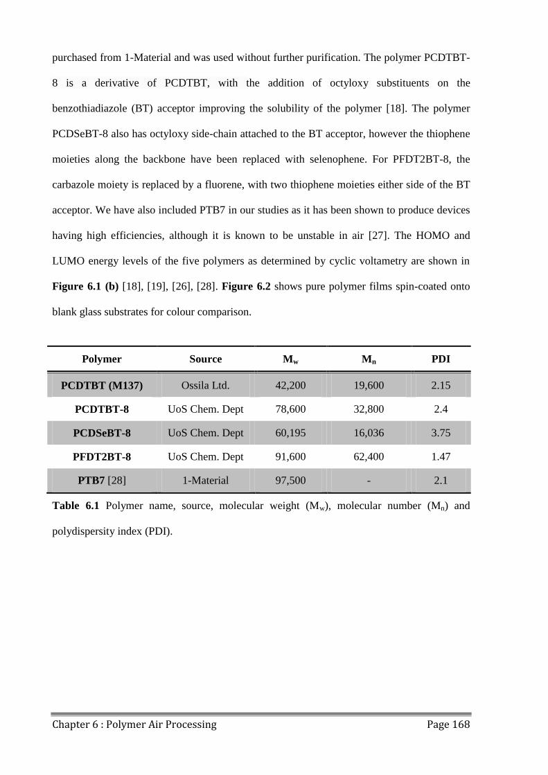
Chapter 6 : Polymer Air Processing Page 168
purchased from 1-Material and was used without further purification. The polymer PCDTBT-
8 is a derivative of PCDTBT, with the addition of octyloxy substituents on the
benzothiadiazole (BT) acceptor improving the solubility of the polymer [18]. The polymer
PCDSeBT-8 also has octyloxy side-chain attached to the BT acceptor, however the thiophene
moieties along the backbone have been replaced with selenophene. For PFDT2BT-8, the
carbazole moiety is replaced by a fluorene, with two thiophene moieties either side of the BT
acceptor. We have also included PTB7 in our studies as it has been shown to produce devices
having high efficiencies, although it is known to be unstable in air [27]. The HOMO and
LUMO energy levels of the five polymers as determined by cyclic voltametry are shown in
Figure 6.1 (b) [18], [19], [26], [28]. Figure 6.2 shows pure polymer films spin-coated onto
blank glass substrates for colour comparison.
Polymer Source Mw Mn PDI
PCDTBT (M137) Ossila Ltd. 42,200 19,600 2.15
PCDTBT-8 UoS Chem. Dept 78,600 32,800 2.4
PCDSeBT-8 UoS Chem. Dept 60,195 16,036 3.75
PFDT2BT-8 UoS Chem. Dept 91,600 62,400 1.47
PTB7 [28] 1-Material 97,500 - 2.1
Table 6.1 Polymer name, source, molecular weight (Mw), molecular number (Mn) and
polydispersity index (PDI).
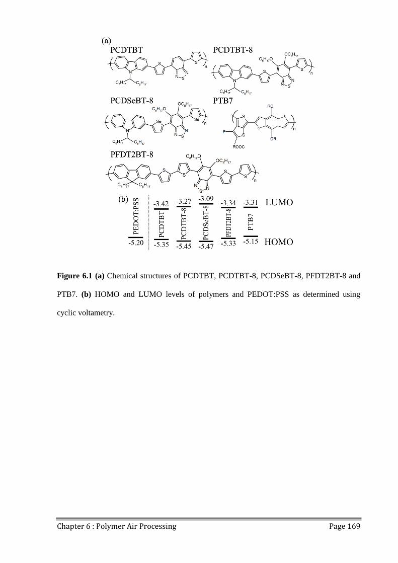
Chapter 6 : Polymer Air Processing Page 169
Figure 6.1 (a) Chemical structures of PCDTBT, PCDTBT-8, PCDSeBT-8, PFDT2BT-8 and
PTB7. (b) HOMO and LUMO levels of polymers and PEDOT:PSS as determined using
cyclic voltametry.
Chapter 6 : Polymer Air Processing Page 170
Figure 6.2 Pure polymer films spin-coated onto blank glass substrates for colour comparison.
6.2 Fabricating OPVs in Air
For each polymer:fullerene blend, six OPV devices were fabricated: three whose active layers
were deposited in the glovebox and three under ambient conditions in a Lamarflo workstation.
OPV devices were based on a standard device architecture of ITO/PEDOT:PSS(30
nm)/active-layer(70-95 nm)/Ca(5 nm)/Al(100 nm). In each case, the active layer was
composed of a polymer:PC70BM blend, with the solvent, material concentration, blend ratio
and film thickness (as determined by detailed optimization studies) recorded in Table 6.2.
PEDOT:PSS was chosen as the HTL material due to its ease of deposition and stability in
completed OPV devices as demonstrated in Chapter 5 : Hole Transport Layer Laboratory
Lifetime Study.
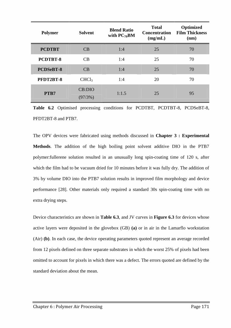
Chapter 6 : Polymer Air Processing Page 171
Polymer Solvent Blend Ratio
with PC70BM
Total
Concentration
(mg/mL)
Optimized
Film Thickness
(nm)
PCDTBT CB 1:4 25 70
PCDTBT-8 CB 1:4 25 70
PCDSeBT-8 CB 1:4 25 70
PFDT2BT-8 CHCl3 1:4 20 70
PTB7 CB:DIO
(97/3%) 1:1.5 25 95
Table 6.2 Optimised processing conditions for PCDTBT, PCDTBT-8, PCDSeBT-8,
PFDT2BT-8 and PTB7.
The OPV devices were fabricated using methods discussed in Chapter 3 : Experimental
Methods. The addition of the high boiling point solvent additive DIO in the PTB7
polymer:fullerene solution resulted in an unusually long spin-coating time of 120 s, after
which the film had to be vacuum dried for 10 minutes before it was fully dry. The addition of
3% by volume DIO into the PTB7 solution results in improved film morphology and device
performance [28]. Other materials only required a standard 30s spin-coating time with no
extra drying steps.
Device characteristics are shown in Table 6.3, and JV curves in Figure 6.3 for devices whose
active layers were deposited in the glovebox (GB) (a) or in air in the Lamarflo workstation
(Air) (b). In each case, the device operating parameters quoted represent an average recorded
from 12 pixels defined on three separate substrates in which the worst 25% of pixels had been
omitted to account for pixels in which there was a defect. The errors quoted are defined by the
standard deviation about the mean.
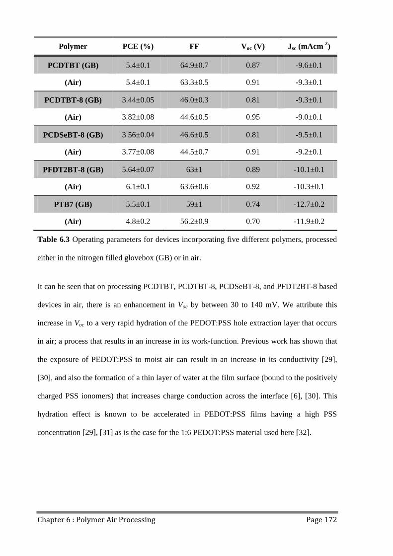
Chapter 6 : Polymer Air Processing Page 172
Polymer PCE (%) FF Voc (V) Jsc (mAcm-2
)
PCDTBT (GB) 5.4±0.1 64.9±0.7 0.87 -9.6±0.1
(Air) 5.4±0.1 63.3±0.5 0.91 -9.3±0.1
PCDTBT-8 (GB) 3.44±0.05 46.0±0.3 0.81 -9.3±0.1
(Air) 3.82±0.08 44.6±0.5 0.95 -9.0±0.1
PCDSeBT-8 (GB) 3.56±0.04 46.6±0.5 0.81 -9.5±0.1
(Air) 3.77±0.08 44.5±0.7 0.91 -9.2±0.1
PFDT2BT-8 (GB) 5.64±0.07 63±1 0.89 -10.1±0.1
(Air) 6.1±0.1 63.6±0.6 0.92 -10.3±0.1
PTB7 (GB) 5.5±0.1 59±1 0.74 -12.7±0.2
(Air) 4.8±0.2 56.2±0.9 0.70 -11.9±0.2
Table 6.3 Operating parameters for devices incorporating five different polymers, processed
either in the nitrogen filled glovebox (GB) or in air.
It can be seen that on processing PCDTBT, PCDTBT-8, PCDSeBT-8, and PFDT2BT-8 based
devices in air, there is an enhancement in Voc by between 30 to 140 mV. We attribute this
increase in Voc to a very rapid hydration of the PEDOT:PSS hole extraction layer that occurs
in air; a process that results in an increase in its work-function. Previous work has shown that
the exposure of PEDOT:PSS to moist air can result in an increase in its conductivity [29],
[30], and also the formation of a thin layer of water at the film surface (bound to the positively
charged PSS ionomers) that increases charge conduction across the interface [6], [30]. This
hydration effect is known to be accelerated in PEDOT:PSS films having a high PSS
concentration [29], [31] as is the case for the 1:6 PEDOT:PSS material used here [32].

Chapter 6 : Polymer Air Processing Page 173
Figure 6.3 Part (a) shows JV characteristics for devices processed in a nitrogen-filled
glovebox, with part (b) showing device characteristics when processed in air.
Thus, we propose that the enhancement of Voc that we observe results from the presence of a
water layer at the PEDOT:PSS film surface that increases its work function; a conclusion in
accord with previous findings using other hole-extraction layers [6]. Notably, the increase in
Voc is largest for the PCDTBT-8 and PCDSeBT-8 based devices, being 140 mV and 100 mV
Chapter 6 : Polymer Air Processing Page 174
respectively. We believe this occurs as a direct result of the deeper HOMO levels of these
polymers (-5.45eV for PCDTBT-8 and -5.47eV for PCDSeBT-8). Here, hole transfer to
“dehydrated” PEDOT:PSS (HOMO at -5.2 eV), is less efficient, resulting in a relatively low
value of Voc (0.81 V) when these devices are processed under nitrogen. When however the
devices are processed in air, the increased work function of “hydrated” PEDOT:PSS results in
more efficient charge extraction and an increase in Voc. In contrast, PCDTBT and PFDT2BT-
8 have a HOMO level that is already close to that of “dehydrated” PEDOT:PSS (-5.35, -5.33
and -5.2 eV respectively) and thus the gain in Voc on processing devices in air is relatively
limited as hole extraction is already relatively efficient. There does not however appear to be
a gain in Voc when processing PTB7 OPV devices in air. Here, the HOMO level of the PTB7
is smaller than that of “dehydrated" PEDOT:PSS (-5.15 and -5.20 eV respectively). On
exposure to moisture, the increase in PEDOT:PSS work-function is likely to further impede
the extraction of holes.
For all the polymers studied (with the exception of PFDT2BT-8), both the Jsc and the FF are
reduced when the active layer blend is deposited in air. This correlates with an overall
reduction in the EQE of the devices that were processed in air as can be seen in Figure 6.4,
measured using the equipment described in 3.6 External Quantum Efficiency (EQE).
Notably however, the Jsc and EQE of PFDT2BT-8 based devices do not appear to be
significantly affected by such air exposure.
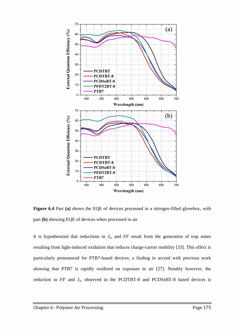
Chapter 6 : Polymer Air Processing Page 175
Figure 6.4 Part (a) shows the EQE of devices processed in a nitrogen-filled glovebox, with
part (b) showing EQE of devices when processed in air.
It is hypothesized that reductions in Jsc and FF result from the generation of trap states
resulting from light-induced oxidation that reduces charge-carrier mobility [33]. This effect is
particularly pronounced for PTB7-based devices; a finding in accord with previous work
showing that PTB7 is rapidly oxidized on exposure in air [27]. Notably however, the
reduction in FF and Jsc observed in the PCDTBT-8 and PCDSeBT-8 based devices is
Chapter 6 : Polymer Air Processing Page 176
counterbalanced by the large increase in Voc, resulting in an overall increase in PCE on
processing in air. For PCDTBT, the smaller gain in Voc is balanced by a comparable reduction
in FF and Jsc, resulting in devices processed under nitrogen and air having similar values of
PCE. For PTB7, the combined effects of a reduction in Voc due to energy level misalignment
at the PEDOT:PSS interface and a reduction of FF and Jsc due to oxidation when processed in
air results in a significant reduction in PCE. Of the five polymers explored, PFDT2BT-8
alone does not undergo a reduction in any of the device metrics, resulting in a higher PCE for
air-processed devices.
6.3 Photostability of Polymers
To explore whether any degradation in efficiency of OPVs fabricated in air could be
correlated with the rate at which the polymer underwent optically induced oxidation, freshly-
spun, un-encapsulated polymer films on quartz substrates were exposed for various times to
light from a solar simulator in air (for 10, 20, 40, 80 and 160 minutes). The optical
transmission of the exposed films was then recorded using a Horiba Fluormax-4
spectrophotometer as described in 3.4 Absorbance Spectroscopy.
To further understand the relative air stability of the different polymers, the changes in their
ability to harvest light as they are deliberately photo-oxidized was studied. This is shown in
Figure 6.5 (a) and (b), where the normalized absorption spectra of the polymer films both
before, and after exposure for 160 minutes to simulated AM1.5 radiation is plotted. In Figure
6.5 (c), the relative absorption of each polymer film (integrated over the wavelength range =
350 to 900 nm) as a function of time during the light exposure, with data normalized to the
absorption determined at t = 0 is shown. It was found that the absorption maxima of each of
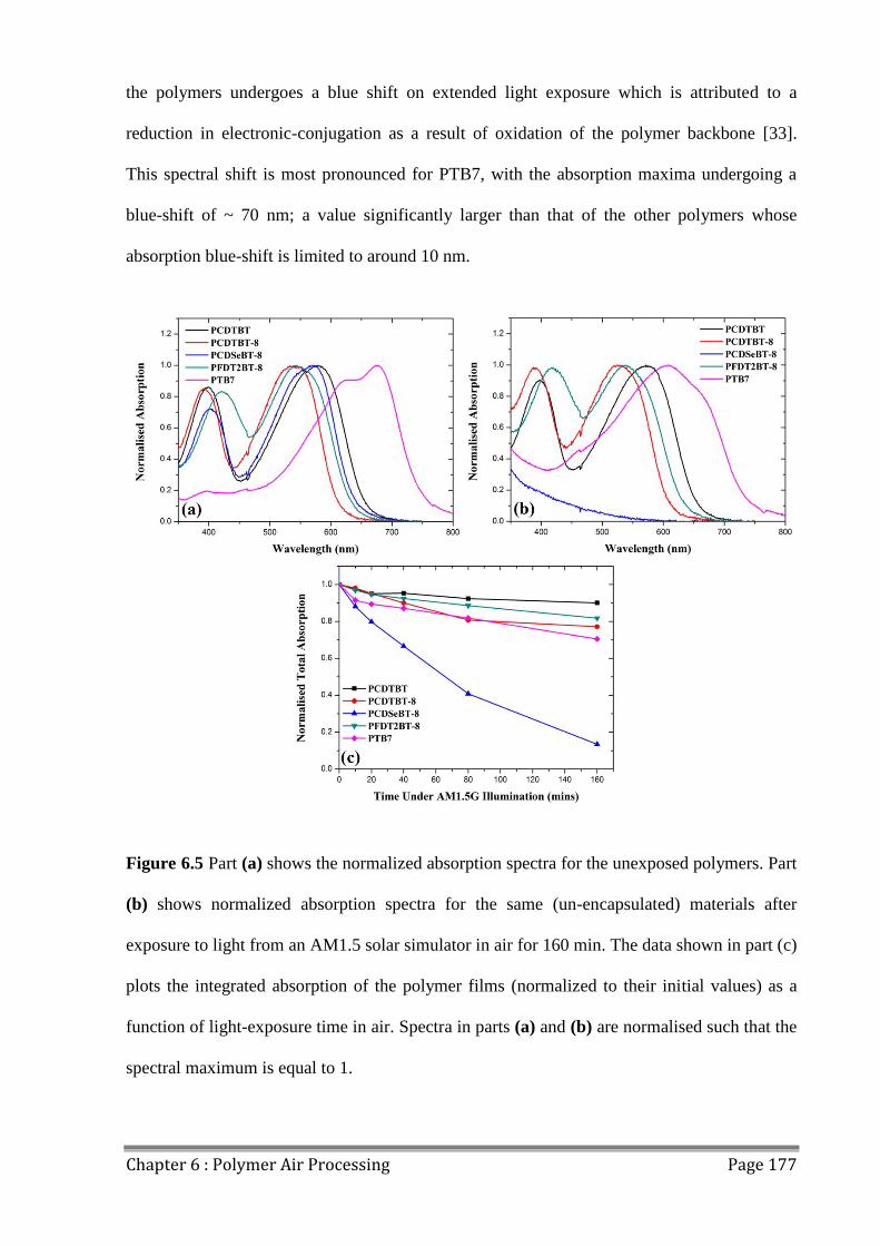
Chapter 6 : Polymer Air Processing Page 177
the polymers undergoes a blue shift on extended light exposure which is attributed to a
reduction in electronic-conjugation as a result of oxidation of the polymer backbone [33].
This spectral shift is most pronounced for PTB7, with the absorption maxima undergoing a
blue-shift of ~ 70 nm; a value significantly larger than that of the other polymers whose
absorption blue-shift is limited to around 10 nm.
Figure 6.5 Part (a) shows the normalized absorption spectra for the unexposed polymers. Part
(b) shows normalized absorption spectra for the same (un-encapsulated) materials after
exposure to light from an AM1.5 solar simulator in air for 160 min. The data shown in part (c)
plots the integrated absorption of the polymer films (normalized to their initial values) as a
function of light-exposure time in air. Spectra in parts (a) and (b) are normalised such that the
spectral maximum is equal to 1.
Chapter 6 : Polymer Air Processing Page 178
In Figure 6.5 (c), it can be seen in that over a relatively short timescale concurrent with spin-
coating in air (< 10 minutes), PCDTBT, PCDTBT-8 and PFDT2BT-8 undergo a small (2 -
3%) but similar reduction in their total absorbance. Notably however, both PTB7 and
PCDSeBT-8 photo-bleach more rapidly, with the absorbance being reduced by 7 and 11%
respectively. At the end of the experiment (160 minutes of illumination), the PCDSeBT-8
sample had become almost totally bleached, thus suggesting it has a poor photostability that is
attributed to the substitution of the thiophene moieties with selenophene. Of all the polymers
explored, PCDTBT undergoes the smallest degree of bleaching over the experiment,
indicating it has the highest degree of photostability. Its polyfluorene analogue PFDT2BT-8
also demonstrates a similar (but slightly reduced) photostability.
6.4 Effects of Extended Air Exposure
To explore the effects of extended air exposure of active layer films on device performance,
OPV devices were fabricated with the same architecture and processing methods as
previously used in this chapter. However, once the active layer had been deposited the
partially completed devices were left in air under ambient conditions for up to 30 minutes. For
reference, devices were also processed in the glovebox and were not exposed to air at any
point during their fabrication. Two polymers were used for this study, PFDT2BT-8 and PTB7.
PFDT2BT-8 was chosen as it was the only polymer studied that did not exhibit a reduction in
operating parameters on processing in air, and PTB7 was chosen for comparison due to its
poor air stability. The average operating parameters for PFDT2BT-8 devices are shown in
Table 6.4 and JV curves in Figure 6.6. Devices with 0 mins exposure time were processed in
the glovebox with no exposure to air at any point during fabrication.
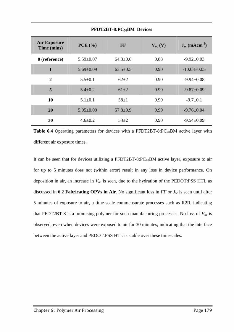
Chapter 6 : Polymer Air Processing Page 179
PFDT2BT-8:PC70BM Devices
Air Exposure
Time (mins) PCE (%) FF Voc (V) Jsc (mAcm
-2)
0 (reference) 5.59±0.07 64.3±0.6 0.88 -9.92±0.03
1 5.69±0.09 63.5±0.5 0.90 -10.03±0.05
2 5.5±0.1 62±2 0.90 -9.94±0.08
5 5.4±0.2 61±2 0.90 -9.87±0.09
10 5.1±0.1 58±1 0.90 -9.7±0.1
20 5.05±0.09 57.8±0.9 0.90 -9.76±0.04
30 4.6±0.2 53±2 0.90 -9.54±0.09
Table 6.4 Operating parameters for devices with a PFDT2BT-8:PC70BM active layer with
different air exposure times.
It can be seen that for devices utilizing a PFDT2BT-8:PC70BM active layer, exposure to air
for up to 5 minutes does not (within error) result in any loss in device performance. On
deposition in air, an increase in Voc is seen, due to the hydration of the PEDOT:PSS HTL as
discussed in 6.2 Fabricating OPVs in Air. No significant loss in FF or Jsc is seen until after
5 minutes of exposure to air, a time-scale commensurate processes such as R2R, indicating
that PFDT2BT-8 is a promising polymer for such manufacturing processes. No loss of Voc is
observed, even when devices were exposed to air for 30 minutes, indicating that the interface
between the active layer and PEDOT:PSS HTL is stable over these timescales.
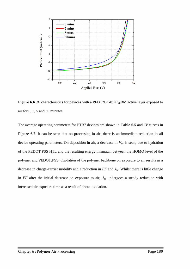
Chapter 6 : Polymer Air Processing Page 180
Figure 6.6 JV characteristics for devices with a PFDT2BT-8:PC70BM active layer exposed to
air for 0, 2, 5 and 30 minutes.
The average operating parameters for PTB7 devices are shown in Table 6.5 and JV curves in
Figure 6.7. It can be seen that on processing in air, there is an immediate reduction in all
device operating parameters. On deposition in air, a decrease in Voc is seen, due to hydration
of the PEDOT:PSS HTL and the resulting energy mismatch between the HOMO level of the
polymer and PEDOT:PSS. Oxidation of the polymer backbone on exposure to air results in a
decrease in charge-carrier mobility and a reduction in FF and Jsc. Whilst there is little change
in FF after the initial decrease on exposure to air, Jsc undergoes a steady reduction with
increased air exposure time as a result of photo-oxidation.
Chapter 6 : Polymer Air Processing Page 181
PTB7:PC70BM Devices
Air Exposure
Time (mins) PCE (%) FF Voc (V) Jsc (mAcm
-2)
0 (reference) 5.64±0.08 60.0±0.5 0.72 -13.06±0.06
1 3.4±0.1 48±1 0.69 -10.31±0.3
2 3.09±0.07 45±1 0.69 -9.98±0.07
5 2.6±0.1 44±1 0.66 -9.63±0.04
10 2.7±0.2 42±2 0.66 -9.6±0.4
20 2.67±0.06 43.5±0.5 0.66 -9.3±0.1
30 2.39±0.06 44.7±0.5 0.66 -8.1±0.1
Table 6.5 Operating parameters for devices with a PTB7:PC70BM active layer with different
air exposure times.
Figure 6.7 JV characteristics for devices with a PTB7:PC70BM active layer exposed to air for
0, 2, 5 and 30 minutes.

Chapter 6 : Polymer Air Processing Page 182
6.5 Conclusions
It was found that carbazole and fluorene based conjugated polymers have a relatively high
degree of photostability that permit them to be processed (in a polymer:fullerene blend) into
the active layer of a photovoltaic device in air with little loss in PCE. Indeed, in some cases,
devices processed in air have enhanced efficiency compared with comparable devices
processed under nitrogen; an affect that is attributed to changes in the work function of the
underlying PEDOT:PSS anode. PFDT2BT-8:PC70BM active layers have been shown to be
stable in air for up to 5 minutes with little loss in device performance. This timeframe is
commensurate with processing timeframes for scale up processes such as R2R printing,
indicating that PFDT2BT-8 is a promising polymer for such manufacturing processes. It will
be interesting to determine whether the photostability of conjugated polymers measured under
optical irradiation in air can be directly correlated with their operational stability when
processed into an OPV device, as this technique could be used as a rapid and efficient
screening tool to identify new polymers for device applications.
Chapter 6 : Polymer Air Processing Page 183
6.6 References
[1] E. Bovill, H. Yi, A. Iraqi, and D. G. Lidzey, “The fabrication of polyfluorene and
polycarbazole-based photovoltaic devices using an air-stable process route,” Appl. Phys. Lett.,
vol. 105, no. 22, p. 223302, Dec. 2014.
[2] V. Chellappan, G. M. Ng, M. J. Tan, W.-P. Goh, and F. Zhu, “Imbalanced charge
mobility in oxygen treated polythiophene/fullerene based bulk heterojunction solar cells,”
Appl. Phys. Lett., vol. 95, no. 26, p. 263305, 2009.
[3] A. Seemann, H.-J. Egelhaaf, C. J. Brabec, and J. A. Hauch, “Influence of oxygen on
semi-transparent organic solar cells with gas permeable electrodes,” Org. Electron., vol. 10,
no. 8, pp. 1424–1428, Dec. 2009.
[4] C. H. Peters, I. T. Sachs-Quintana, W. R. Mateker, T. Heumueller, J. Rivnay, R.
Noriega, Z. M. Beiley, E. T. Hoke, A. Salleo, and M. D. McGehee, “The mechanism of burn-
in loss in a high efficiency polymer solar cell,” Adv. Mater., vol. 24, no. 5, pp. 663–668, Feb.
2012.
[5] F. C. Krebs and K. Norrman, “Analysis of the Failure Mechanism for a Stable Organic
Photovoltaic During 10 000 h of Testing,” no. September, pp. 697–712, 2007.
[6] E. S. R. Bovill, J. Griffin, T. Wang, J. W. Kingsley, H. Yi, A. Iraqi, A. R. Buckley,
and D. G. Lidzey, “Air processed organic photovoltaic devices incorporating a MoOx anode
buffer layer,” Appl. Phys. Lett., vol. 102, no. 18, p. 183303, May 2013.
[7] J. M. Ball, R. K. M. Bouwer, F. B. Kooistra, J. M. Frost, Y. Qi, E. B. Domingo, J.
Smith, D. M. De Leeuw, J. C. Hummelen, J. Nelson, A. Kahn, N. Stingelin, D. D. C. Bradley,
Chapter 6 : Polymer Air Processing Page 184
and T. D. Anthopoulos, “Soluble fullerene derivatives: The effect of electronic structure on
transistor performance and air stability,” J. Appl. Phys., vol. 110, no. 2011, 2011.
[8] M. C. Scharber, D. Mühlbacher, M. Koppe, P. Denk, C. Waldauf, A. J. Heeger, and C.
J. Brabec, “Design Rules for Donors in Bulk-Heterojunction Solar Cells—Towards 10 %
Energy-Conversion Efficiency,” Adv. Mater., vol. 18, no. 6, pp. 789–794, Mar. 2006.
[9] N. Blouin, A. Michaud, and M. Leclerc, “A Low-Bandgap Poly(2,7-Carbazole)
Derivative for Use in High-Performance Solar Cells,” Adv. Mater., vol. 19, no. 17, pp. 2295–
2300, Sep. 2007.
[10] D. C. Watters, J. Kingsley, H. Yi, T. Wang, A. Iraqi, and D. Lidzey, “Optimising the
efficiency of carbazole co-polymer solar-cells by control over the metal cathode electrode,”
Org. Electron., vol. 13, no. 8, pp. 1401–1408, Aug. 2012.
[11] T. Wang, A. J. Pearson, A. D. F. Dunbar, P. A. Staniec, D. C. Watters, H. Yi, A. J.
Ryan, R. A. L. Jones, A. Iraqi, and D. G. Lidzey, “Correlating Structure with Function in
Thermally Annealed PCDTBT:PC70BM Photovoltaic Blends,” Adv. Funct. Mater., vol. 22,
no. 7, pp. 1399–1408, Apr. 2012.
[12] S. H. Park, A. Roy, S. Beaupré, S. Cho, N. Coates, J. S. Moon, D. Moses, M. Leclerc,
K. Lee, and A. J. Heeger, “Bulk heterojunction solar cells with internal quantum efficiency
approaching 100%,” Nat. Photonics, vol. 3, no. 5, pp. 297–302, Apr. 2009.
[13] J. Liu, S. Shao, G. Fang, B. Meng, Z. Xie, and L. Wang, “High-efficiency inverted
polymer solar cells with transparent and work-function tunable MoO(3)-Al composite film as
cathode buffer layer.,” Adv. Mater., vol. 24, no. 20, pp. 2774–9, May 2012.
Chapter 6 : Polymer Air Processing Page 185
[14] Y. Sun, J. H. Seo, C. J. Takacs, J. Seifter, and A. J. Heeger, “Inverted polymer solar
cells integrated with a low-temperature-annealed sol-gel-derived ZnO film as an electron
transport layer,” Adv. Mater., vol. 23, no. 14, pp. 1679–1683, Apr. 2011.
[15] Y. Sun, C. J. Takacs, S. R. Cowan, J. H. Seo, X. Gong, A. Roy, and A. J. Heeger,
“Efficient, air-stable bulk heterojunction polymer solar cells using MoO x as the anode
interfacial layer,” Adv. Mater., vol. 23, no. 19, pp. 2226–2230, May 2011.
[16] C. H. Peters, I. T. Sachs-Quintana, J. P. Kastrop, S. Beaupré, M. Leclerc, and M. D.
McGehee, “High Efficiency Polymer Solar Cells with Long Operating Lifetimes,” Adv.
Energy Mater., vol. 1, no. 4, pp. 491–494, Jul. 2011.
[17] S. Cho, J. H. Seo, S. H. Park, S. Beaupré, M. Leclerc, and A. J. Heeger, “A thermally
stable semiconducting polymer.,” Adv. Mater., vol. 22, no. 11, pp. 1253–7, Mar. 2010.
[18] H. Yi, S. Al-Faifi, A. Iraqi, D. C. Watters, J. Kingsley, and D. G. Lidzey, “Carbazole
and thienyl benzo[1,2,5]thiadiazole based polymers with improved open circuit voltages and
processability for application in solar cells,” J. Mater. Chem., vol. 21, no. 35, p. 13649, 2011.
[19] D. C. Watters, H. Yi, A. J. Pearson, J. Kingsley, A. Iraqi, and D. Lidzey, “Fluorene-
based co-polymer with high hole mobility and device performance in bulk heterojunction
organic solar cells.,” Macromol. Rapid Commun., vol. 34, no. 14, pp. 1157–62, Jul. 2013.
[20] Z. Chen, H. Lemke, S. Albert-Seifried, M. Caironi, M. M. Nielsen, M. Heeney, W.
Zhang, I. McCulloch, and H. Sirringhaus, “High mobility ambipolar charge transport in
polyselenophene conjugated polymers.,” Adv. Mater., vol. 22, no. 21, pp. 2371–5, Jun. 2010.
Chapter 6 : Polymer Air Processing Page 186
[21] Q. Hou, Y. Xu, W. Yang, M. Yuan, J. Peng, and Y. Cao, “Novel red-emitting
fluorene-based copolymers,” J. Mater. Chem., vol. 12, no. 10, pp. 2887–2892, Sep. 2002.
[22] M. Bernius, M. Inbasekaran, E. Woo, W. Wu, and L. Wujkowski, “Fluorene-based
polymers-preparation and applications,” J. Mater. Sci. Mater. Electron., vol. 11, no. 2, pp.
111–116, 2000.
[23] G. Klärner, J.-I. Lee, M. H. Davey, and R. D. Miller, “Exciton Migration and
Trapping in Copolymers Based on Dialkylfluorenes,” Adv. Mater., vol. 11, no. 2, pp. 115–
119, Feb. 1999.
[24] W.-Y. Wong, “Metallated molecular materials of fluorene derivatives and their
analogues,” Coord. Chem. Rev., vol. 249, no. 9–10, pp. 971–997, May 2005.
[25] S. Alem, T.-Y. Chu, S. C. Tse, S. Wakim, J. Lu, R. Movileanu, Y. Tao, F. Bélanger,
D. Désilets, S. Beaupré, M. Leclerc, S. Rodman, D. Waller, and R. Gaudiana, “Effect of
mixed solvents on PCDTBT:PC70BM based solar cells,” Org. Electron., vol. 12, no. 11, pp.
1788–1793, Nov. 2011.
[26] A. A. B. Alghamdi, D. C. Watters, H. Yi, S. Al-Faifi, M. S. Almeataq, D. Coles, J.
Kingsley, D. G. Lidzey, and A. Iraqi, “Selenophene vs. thiophene in benzothiadiazole-based
low energy gap donor–acceptor polymers for photovoltaic applications,” J. Mater. Chem. A,
vol. 1, no. 16, p. 5165, 2013.
[27] Y. W. Soon, H. Cho, J. Low, H. Bronstein, I. McCulloch, and J. R. Durrant,
“Correlating triplet yield, singlet oxygen generation and photochemical stability in
polymer/fullerene blend films.,” Chem. Commun. (Camb)., vol. 49, no. 13, pp. 1291–3, Feb.
2013.

Chapter 6 : Polymer Air Processing Page 187
[28] Y. Liang, Z. Xu, J. Xia, S.-T. Tsai, Y. Wu, G. Li, C. Ray, and L. Yu, “For the bright
future-bulk heterojunction polymer solar cells with power conversion efficiency of 7.4%.,”
Adv. Mater., vol. 22, no. 20, pp. E135–8, May 2010.
[29] A. M. Nardes, M. Kemerink, M. M. de Kok, E. Vinken, K. Maturova, and R. A. J.
Janssen, “Conductivity, work function, and environmental stability of PEDOT:PSS thin films
treated with sorbitol,” Org. Electron., vol. 9, no. 5, pp. 727–734, Oct. 2008.
[30] M. Kuş and S. Okur, “Electrical characterization of PEDOT:PSS beyond humidity
saturation,” Sensors Actuators B Chem., vol. 143, no. 1, pp. 177–181, Dec. 2009.
[31] J. Huang, P. F. Miller, J. S. Wilson, A. J. de Mello, J. C. de Mello, and D. D. C.
Bradley, “Investigation of the Effects of Doping and Post-Deposition Treatments on the
Conductivity, Morphology, and Work Function of Poly(3,4-
ethylenedioxythiophene)/Poly(styrene sulfonate) Films,” Adv. Funct. Mater., vol. 15, no. 2,
pp. 290–296, Feb. 2005.
[32] “PEDOT:PSS - Heraeus CleviosTM
P VP Al 4083.” [Online]. Available:
http://www.heraeus-
clevios.com/en/_technik/productdetail_1034017.aspx?psMarketId=1286&psApplicationId=.
[33] E. T. Hoke, I. T. Sachs-Quintana, M. T. Lloyd, I. Kauvar, W. R. Mateker, A. M.
Nardes, C. H. Peters, N. Kopidakis, and M. D. McGehee, “The Role of Electron Affinity in
Determining Whether Fullerenes Catalyze or Inhibit Photooxidation of Polymers for Solar
Cells,” Adv. Energy Mater., vol. 2, no. 11, pp. 1351–1357, Nov. 2012.

Page 188
Chapter 7 : Outdoor Lifetime Testing Page 189
Chapter 7 : Outdoor Lifetime Testing
In Chapter 5 : Hole Transport Layer Laboratory Lifetime Study, the operational lifetimes
of OPV devices utilising a PCDTBT:PC70BM active layer and three different hole transport
layers were investigated using a laboratory lifetime testing setup. From this test, it was shown
that PEDOT:PSS resulted in devices having the longest extrapolated T80 lifetimes of ~ 7.2
years. In Chapter 6 : Polymer Air Processing, it was shown that devices with a PFDT2BT-
8:PC70BM active layer had the highest PCE of all the polymers tested and were extremely
stable when processed in air. Utilising these materials, devices with an
ITO/PEDOT:PSS/PFDT2BT-8:PC70BM/Ca/Al architecture were fabricated and installed in
an outdoor testing setup, as described in 3.10 Outdoor Lifetime Testing, on the roof of the
Department of Physics at the University of Sheffield, England, UK, for a period of four
months. It was shown that daily and seasonal light intensity and temperature variation has a
significant effect on measured Jsc, FF, Voc and PCE, and the calculation of device T80 lifetime.

Chapter 7 : Outdoor Lifetime Testing Page 190
7.0 Introduction
In comparison to laboratory testing of OPV devices, outdoor testing is more representative of
the real-world conditions that commercial devices would experience during their operational
lifetime. However, only a few such studies have been carried out so far [1]–[5], almost all
with a P3HT:PCBM active layer blend on flexible PET substrates, with T80 lifetimes of up to
10,000 hours calculated for the best performing devices [1]. Outdoor testing of OPV devices
introduces many challenges that are not present in laboratory testing. The increased humidity
and the presence of precipitation in outdoor environments (especially in temperate countries)
stresses the encapsulation of OPV devices, and is often the cause of catastrophic device
failure [1]. Daily thermal cycling also introduces degradation mechanisms and efficiency
measurement issues, discussed in more detail in 7.2 Temperature Effects.
Here, four devices based on an ITO/PEDOT:PSS/PFDT2BT-8:PC70BM/Ca/Al architecture
were tested under conditions closely modelled on the ISOS-O-2 specifications [6], outlined in
3.11.2 ISOS Outdoor Testing. The outdoor testing setup used did not expose the OPV
devices to atmospheric conditions, but enclosed them in an environmental chamber filled with
an overpressure of nitrogen at close to 0% humidity. This was to exclude extrinsic
degradation processes, such as water and oxygen ingress, and allow for study of intrinsic
degradation processes under outdoor conditions. The data presented here is for the first four
months of an ongoing study.
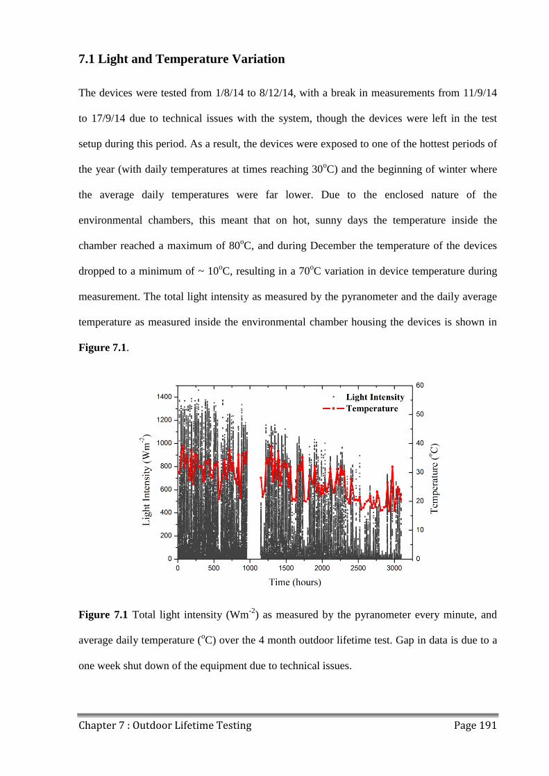
Chapter 7 : Outdoor Lifetime Testing Page 191
7.1 Light and Temperature Variation
The devices were tested from 1/8/14 to 8/12/14, with a break in measurements from 11/9/14
to 17/9/14 due to technical issues with the system, though the devices were left in the test
setup during this period. As a result, the devices were exposed to one of the hottest periods of
the year (with daily temperatures at times reaching 30oC) and the beginning of winter where
the average daily temperatures were far lower. Due to the enclosed nature of the
environmental chambers, this meant that on hot, sunny days the temperature inside the
chamber reached a maximum of 80oC, and during December the temperature of the devices
dropped to a minimum of ~ 10oC, resulting in a 70
oC variation in device temperature during
measurement. The total light intensity as measured by the pyranometer and the daily average
temperature as measured inside the environmental chamber housing the devices is shown in
Figure 7.1.
Figure 7.1 Total light intensity (Wm-2
) as measured by the pyranometer every minute, and
average daily temperature (oC) over the 4 month outdoor lifetime test. Gap in data is due to a
one week shut down of the equipment due to technical issues.
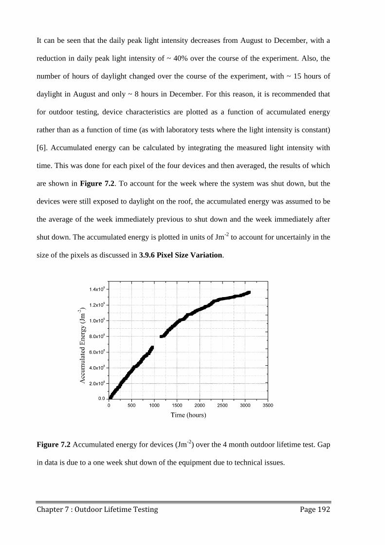
Chapter 7 : Outdoor Lifetime Testing Page 192
It can be seen that the daily peak light intensity decreases from August to December, with a
reduction in daily peak light intensity of ~ 40% over the course of the experiment. Also, the
number of hours of daylight changed over the course of the experiment, with ~ 15 hours of
daylight in August and only ~ 8 hours in December. For this reason, it is recommended that
for outdoor testing, device characteristics are plotted as a function of accumulated energy
rather than as a function of time (as with laboratory tests where the light intensity is constant)
[6]. Accumulated energy can be calculated by integrating the measured light intensity with
time. This was done for each pixel of the four devices and then averaged, the results of which
are shown in Figure 7.2. To account for the week where the system was shut down, but the
devices were still exposed to daylight on the roof, the accumulated energy was assumed to be
the average of the week immediately previous to shut down and the week immediately after
shut down. The accumulated energy is plotted in units of Jm-2
to account for uncertainly in the
size of the pixels as discussed in 3.9.6 Pixel Size Variation.
Figure 7.2 Accumulated energy for devices (Jm-2
) over the 4 month outdoor lifetime test. Gap
in data is due to a one week shut down of the equipment due to technical issues.
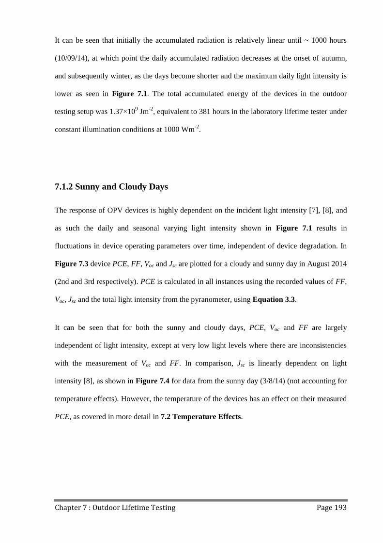
Chapter 7 : Outdoor Lifetime Testing Page 193
It can be seen that initially the accumulated radiation is relatively linear until ~ 1000 hours
(10/09/14), at which point the daily accumulated radiation decreases at the onset of autumn,
and subsequently winter, as the days become shorter and the maximum daily light intensity is
lower as seen in Figure 7.1. The total accumulated energy of the devices in the outdoor
testing setup was 1.37×10⁹ Jm
-2, equivalent to 381 hours in the laboratory lifetime tester under
constant illumination conditions at 1000 Wm-2
.
7.1.2 Sunny and Cloudy Days
The response of OPV devices is highly dependent on the incident light intensity [7], [8], and
as such the daily and seasonal varying light intensity shown in Figure 7.1 results in
fluctuations in device operating parameters over time, independent of device degradation. In
Figure 7.3 device PCE, FF, Voc and Jsc are plotted for a cloudy and sunny day in August 2014
(2nd and 3rd respectively). PCE is calculated in all instances using the recorded values of FF,
Voc, Jsc and the total light intensity from the pyranometer, using Equation 3.3.
It can be seen that for both the sunny and cloudy days, PCE, Voc and FF are largely
independent of light intensity, except at very low light levels where there are inconsistencies
with the measurement of Voc and FF. In comparison, Jsc is linearly dependent on light
intensity [8], as shown in Figure 7.4 for data from the sunny day (3/8/14) (not accounting for
temperature effects). However, the temperature of the devices has an effect on their measured
PCE, as covered in more detail in 7.2 Temperature Effects.
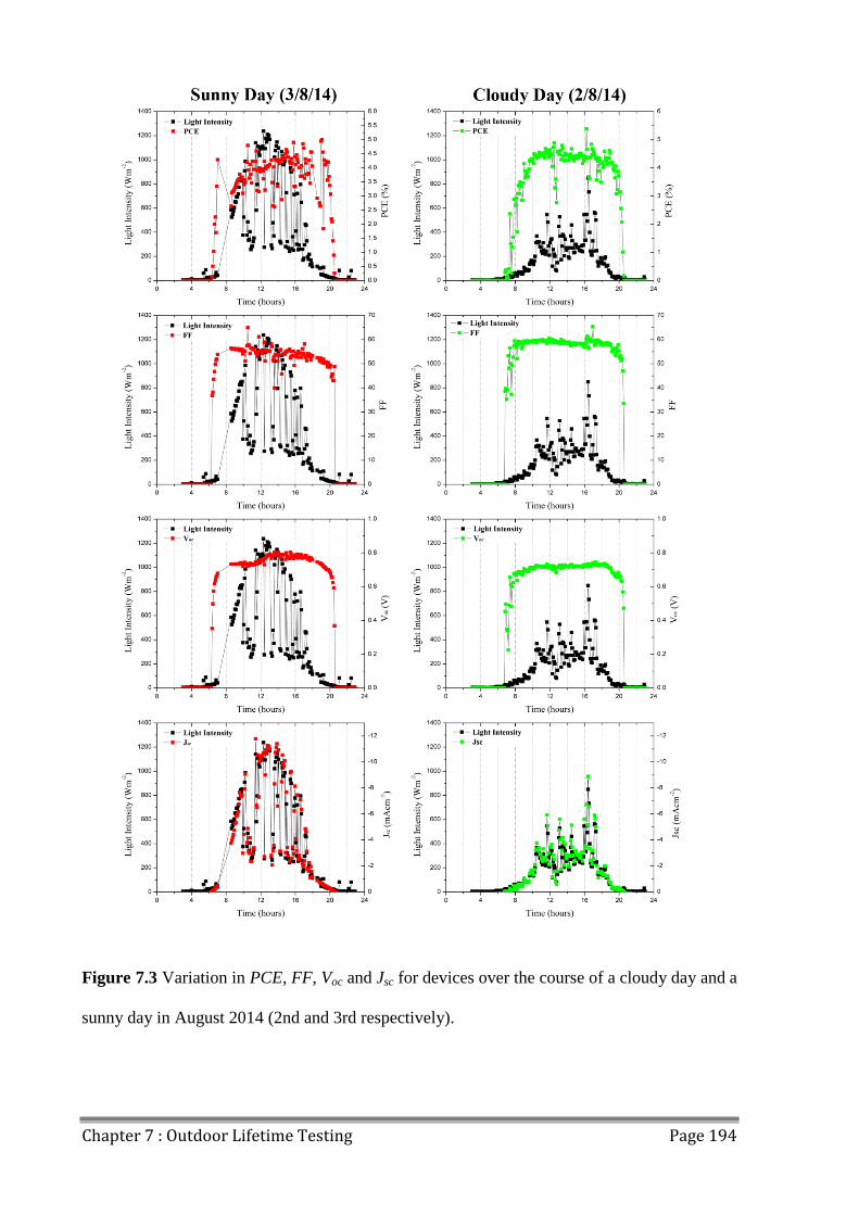
Chapter 7 : Outdoor Lifetime Testing Page 194
Figure 7.3 Variation in PCE, FF, Voc and Jsc for devices over the course of a cloudy day and a
sunny day in August 2014 (2nd and 3rd respectively).
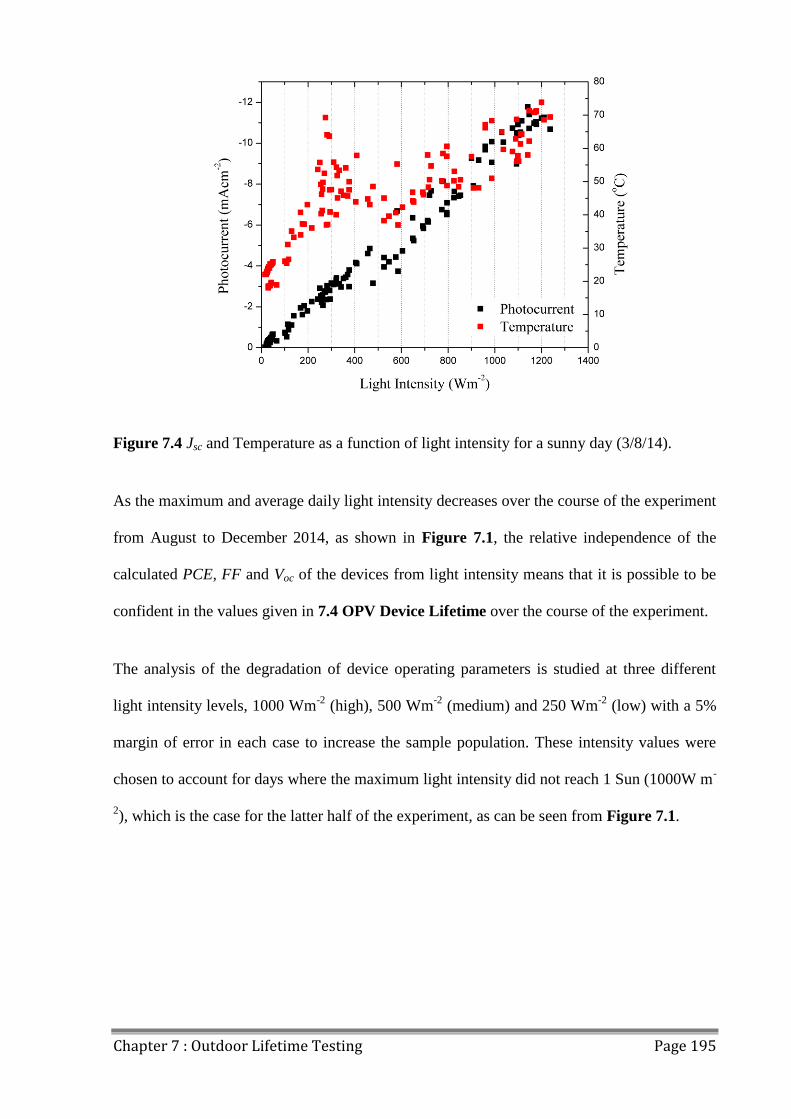
Chapter 7 : Outdoor Lifetime Testing Page 195
Figure 7.4 Jsc and Temperature as a function of light intensity for a sunny day (3/8/14).
As the maximum and average daily light intensity decreases over the course of the experiment
from August to December 2014, as shown in Figure 7.1, the relative independence of the
calculated PCE, FF and Voc of the devices from light intensity means that it is possible to be
confident in the values given in 7.4 OPV Device Lifetime over the course of the experiment.
The analysis of the degradation of device operating parameters is studied at three different
light intensity levels, 1000 Wm-2
(high), 500 Wm-2
(medium) and 250 Wm-2
(low) with a 5%
margin of error in each case to increase the sample population. These intensity values were
chosen to account for days where the maximum light intensity did not reach 1 Sun (1000W m-
2), which is the case for the latter half of the experiment, as can be seen from Figure 7.1.
Chapter 7 : Outdoor Lifetime Testing Page 196
7.2 Temperature Effects
A major issue with outdoor testing of OPVs is thermal cycling over the course of every day,
especially for the setup used here due to the enclosed nature of the environmental chamber
and the resulting high internal temperatures. High temperatures can cause thermal annealing
of active layer materials in the device [9], and induce mechanical stresses due to different
thermal expansion coefficients of the materials, which can lead to delamination at interfaces
and device failure. Indeed, thermal cycling and its effects on OPV devices is such an
important factor when calculating the real-world stability of OPV devices that it is the subject
of its own ISOS testing protocol, ISOS-T [6]. Device temperatures for the 2nd August (cloudy
day) and 3rd August (sunny day) days are shown in Figure 7.5.
Figure 7.5 Variation in temperature for devices over the course of a cloudy day and a sunny
day in August 2014 (2nd and 3rd respectively).
It can be seen that the temperature is highly dependent on light intensity due to the enclosed
nature of the environmental chamber housing the OPV devices. For the sunny day shown
here, the maximum temperature reached was 73.9oC with an average temperature of 36.5
oC,
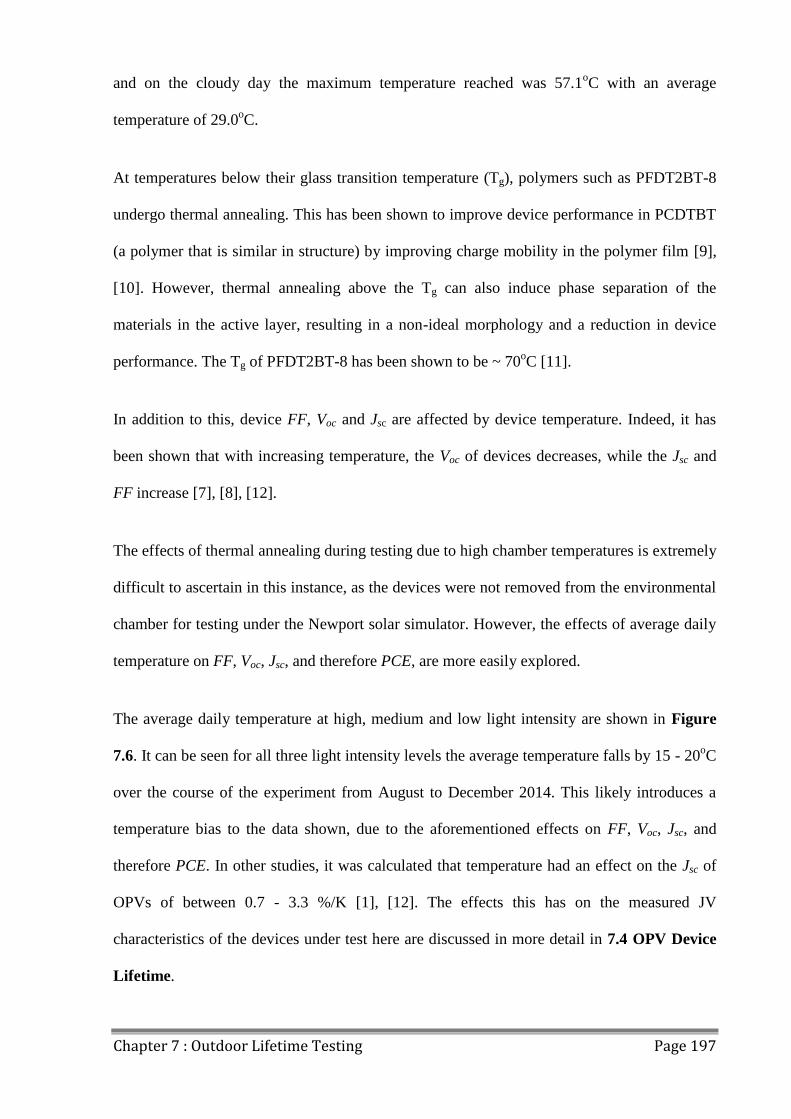
Chapter 7 : Outdoor Lifetime Testing Page 197
and on the cloudy day the maximum temperature reached was 57.1oC with an average
temperature of 29.0oC.
At temperatures below their glass transition temperature (Tg), polymers such as PFDT2BT-8
undergo thermal annealing. This has been shown to improve device performance in PCDTBT
(a polymer that is similar in structure) by improving charge mobility in the polymer film [9],
[10]. However, thermal annealing above the Tg can also induce phase separation of the
materials in the active layer, resulting in a non-ideal morphology and a reduction in device
performance. The Tg of PFDT2BT-8 has been shown to be ~ 70oC [11].
In addition to this, device FF, Voc and Jsc are affected by device temperature. Indeed, it has
been shown that with increasing temperature, the Voc of devices decreases, while the Jsc and
FF increase [7], [8], [12].
The effects of thermal annealing during testing due to high chamber temperatures is extremely
difficult to ascertain in this instance, as the devices were not removed from the environmental
chamber for testing under the Newport solar simulator. However, the effects of average daily
temperature on FF, Voc, Jsc, and therefore PCE, are more easily explored.
The average daily temperature at high, medium and low light intensity are shown in Figure
7.6. It can be seen for all three light intensity levels the average temperature falls by 15 - 20oC
over the course of the experiment from August to December 2014. This likely introduces a
temperature bias to the data shown, due to the aforementioned effects on FF, Voc, Jsc, and
therefore PCE. In other studies, it was calculated that temperature had an effect on the Jsc of
OPVs of between 0.7 - 3.3 %/K [1], [12]. The effects this has on the measured JV
characteristics of the devices under test here are discussed in more detail in 7.4 OPV Device
Lifetime.
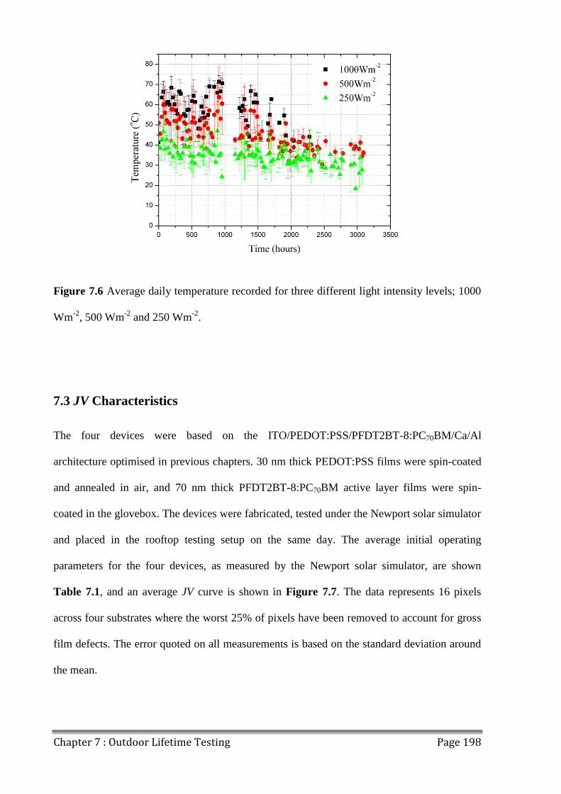
Chapter 7 : Outdoor Lifetime Testing Page 198
Figure 7.6 Average daily temperature recorded for three different light intensity levels; 1000
Wm-2
, 500 Wm-2
and 250 Wm-2
.
7.3 JV Characteristics
The four devices were based on the ITO/PEDOT:PSS/PFDT2BT-8:PC70BM/Ca/Al
architecture optimised in previous chapters. 30 nm thick PEDOT:PSS films were spin-coated
and annealed in air, and 70 nm thick PFDT2BT-8:PC70BM active layer films were spin-
coated in the glovebox. The devices were fabricated, tested under the Newport solar simulator
and placed in the rooftop testing setup on the same day. The average initial operating
parameters for the four devices, as measured by the Newport solar simulator, are shown
Table 7.1, and an average JV curve is shown in Figure 7.7. The data represents 16 pixels
across four substrates where the worst 25% of pixels have been removed to account for gross
film defects. The error quoted on all measurements is based on the standard deviation around
the mean.
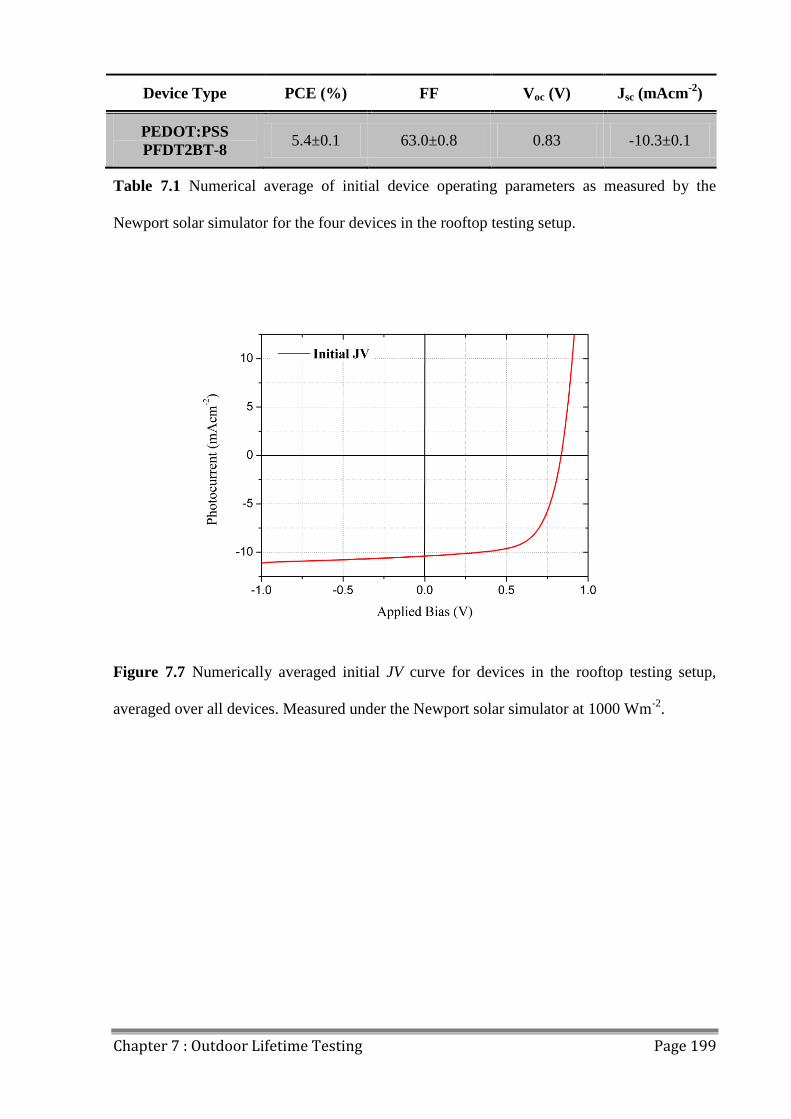
Chapter 7 : Outdoor Lifetime Testing Page 199
Device Type PCE (%) FF Voc (V) Jsc (mAcm-2
)
PEDOT:PSS
PFDT2BT-8 5.4±0.1 63.0±0.8 0.83 -10.3±0.1
Table 7.1 Numerical average of initial device operating parameters as measured by the
Newport solar simulator for the four devices in the rooftop testing setup.
Figure 7.7 Numerically averaged initial JV curve for devices in the rooftop testing setup,
averaged over all devices. Measured under the Newport solar simulator at 1000 Wm-2
.
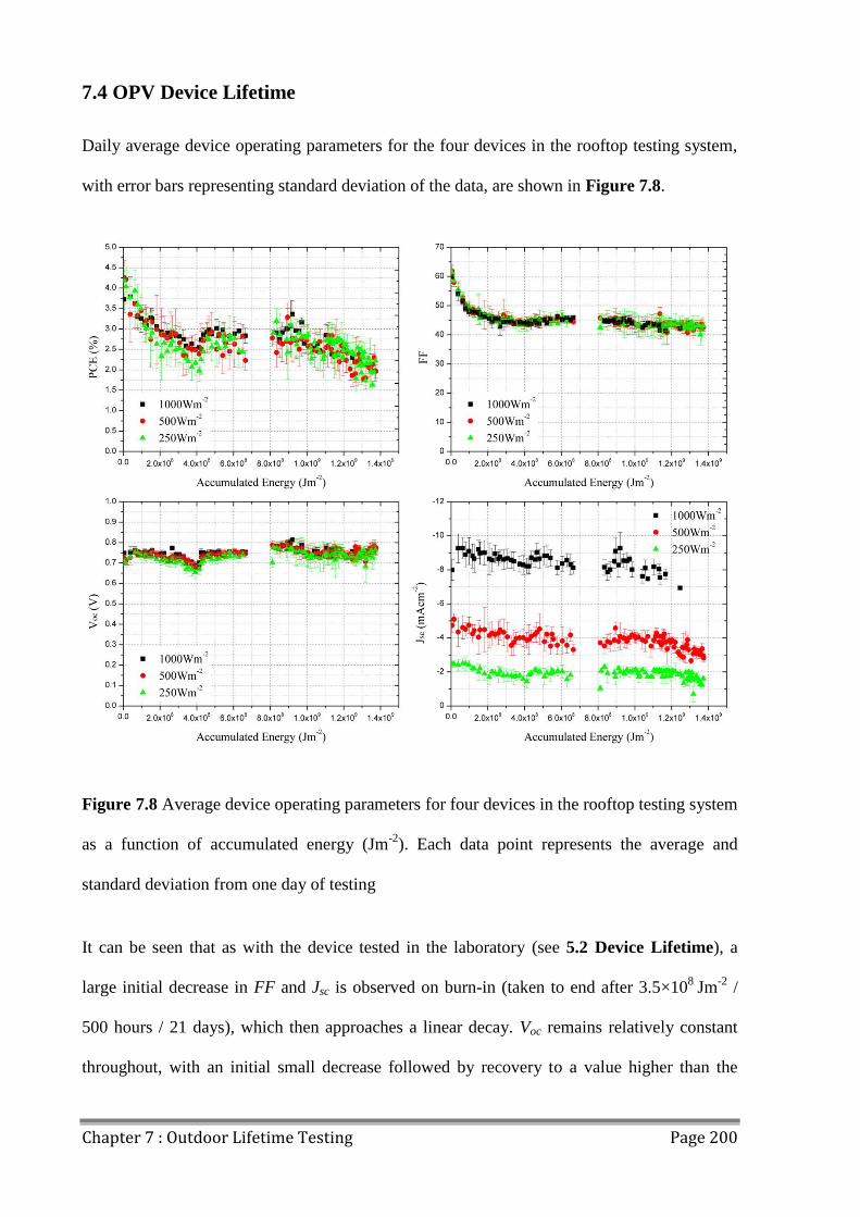
Chapter 7 : Outdoor Lifetime Testing Page 200
7.4 OPV Device Lifetime
Daily average device operating parameters for the four devices in the rooftop testing system,
with error bars representing standard deviation of the data, are shown in Figure 7.8.
Figure 7.8 Average device operating parameters for four devices in the rooftop testing system
as a function of accumulated energy (Jm-2
). Each data point represents the average and
standard deviation from one day of testing
It can be seen that as with the device tested in the laboratory (see 5.2 Device Lifetime), a
large initial decrease in FF and Jsc is observed on burn-in (taken to end after 3.5×10⁸
Jm-2
/
500 hours / 21 days), which then approaches a linear decay. Voc remains relatively constant
throughout, with an initial small decrease followed by recovery to a value higher than the
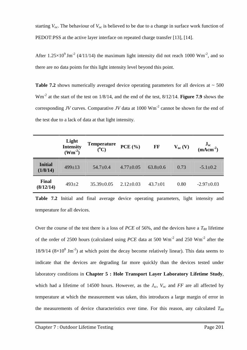
Chapter 7 : Outdoor Lifetime Testing Page 201
starting Voc. The behaviour of Voc is believed to be due to a change in surface work function of
PEDOT:PSS at the active layer interface on repeated charge transfer [13], [14].
After 1.25×10⁹
Jm-2
(4/11/14) the maximum light intensity did not reach 1000 Wm-2
, and so
there are no data points for this light intensity level beyond this point.
Table 7.2 shows numerically averaged device operating parameters for all devices at ~ 500
Wm-2
at the start of the test on 1/8/14, and the end of the test, 8/12/14. Figure 7.9 shows the
corresponding JV curves. Comparative JV data at 1000 Wm-2
cannot be shown for the end of
the test due to a lack of data at that light intensity.
Light
Intensity
(Wm-2
)
Temperature
(oC)
PCE (%) FF Voc (V) Jsc
(mAcm-2
)
Initial
(1/8/14) 499±13 54.7±0.4 4.77±0.05 63.8±0.6 0.73 -5.1±0.2
Final
(8/12/14) 493±2 35.39±0.05 2.12±0.03 43.7±01 0.80 -2.97±0.03
Table 7.2 Initial and final average device operating parameters, light intensity and
temperature for all devices.
Over the course of the test there is a loss of PCE of 56%, and the devices have a T80 lifetime
of the order of 2500 hours (calculated using PCE data at 500 Wm-2
and 250 Wm-2
after the
18/9/14 (8×10⁸ Jm
-2) at which point the decay become relatively linear). This data seems to
indicate that the devices are degrading far more quickly than the devices tested under
laboratory conditions in Chapter 5 : Hole Transport Layer Laboratory Lifetime Study,
which had a lifetime of 14500 hours. However, as the Jsc, Voc and FF are all affected by
temperature at which the measurement was taken, this introduces a large margin of error in
the measurements of device characteristics over time. For this reason, any calculated T80
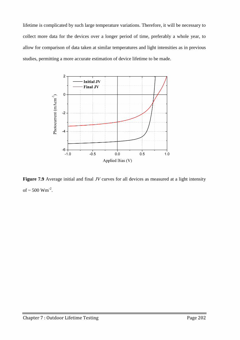
Chapter 7 : Outdoor Lifetime Testing Page 202
lifetime is complicated by such large temperature variations. Therefore, it will be necessary to
collect more data for the devices over a longer period of time, preferably a whole year, to
allow for comparison of data taken at similar temperatures and light intensities as in previous
studies, permitting a more accurate estimation of device lifetime to be made.
Figure 7.9 Average initial and final JV curves for all devices as measured at a light intensity
of ~ 500 Wm-2
.
Chapter 7 : Outdoor Lifetime Testing Page 203
7.5 Conclusions
In summary, initial and preliminary measurements of the stability and degradation of OPV
devices when tested outdoors under conditions closely modelled on the ISOS-O-2 test have
been made. The effects of daily and seasonal light intensity and temperature variation on
device performance are investigated, and have been shown to have a marked effect on the
measurement of device JV characteristics. The effects of daily fluctuations in light intensity
on JV characteristics have been observed, and it was shown that FF and Voc are largely
independent, though Jsc is extremely dependent on light intensity. T80 lifetimes of ~ 2500
hours are calculated, however, more data over a longer period is required to remove JV
measurement bias introduced by seasonal variations in temperature. The test is currently
ongoing, with plans to extend it up to one year to acquire the necessary data to make an
accurate calculation of device T80 lifetime.
Chapter 7 : Outdoor Lifetime Testing Page 204
7.6 References
[1] S. A. Gevorgyan, M. V. Madsen, H. F. Dam, M. Jørgensen, C. J. Fell, K. F. Anderson,
B. C. Duck, A. Mescheloff, E. A. Katz, A. Elschner, R. Roesch, H. Hoppe, M. Hermenau, M.
Riede, and F. C. Krebs, “Interlaboratory outdoor stability studies of flexible roll-to-roll coated
organic photovoltaic modules: Stability over 10,000h,” Sol. Energy Mater. Sol. Cells, vol.
116, pp. 187–196, Sep. 2013.
[2] D. Angmo, P. M. Sommeling, R. Gupta, M. Hösel, S. A. Gevorgyan, J. M. Kroon, G.
U. Kulkarni, and F. C. Krebs, “Outdoor Operational Stability of Indium-Free Flexible
Polymer Solar Modules Over 1 Year Studied in India, Holland, and Denmark,” Adv. Eng.
Mater., vol. 16, no. 8, pp. 976–987, Aug. 2014.
[3] J. A. Hauch, P. Schilinsky, S. A. Choulis, R. Childers, M. Biele, and C. J. Brabec,
“Flexible organic P3HT:PCBM bulk-heterojunction modules with more than 1 year outdoor
lifetime,” Sol. Energy Mater. Sol. Cells, vol. 92, no. 7, pp. 727–731, Jul. 2008.
[4] R. R. Søndergaard, T. Makris, P. Lianos, A. Manor, E. A. Katz, W. Gong, S. M.
Tuladhar, J. Nelson, R. Tuomi, P. Sommeling, S. C. Veenstra, A. Rivaton, A. Dupuis, G.
Teran-Escobar, M. Lira-Cantu, S. B. Sapkota, B. Zimmermann, U. Würfel, A. Matzarakis,
and F. C. Krebs, “The use of polyurethane as encapsulating method for polymer solar cells—
An inter laboratory study on outdoor stability in 8 countries,” Sol. Energy Mater. Sol. Cells,
vol. 99, pp. 292–300, Apr. 2012.
[5] M. V. Madsen, S. A. Gevorgyan, R. Pacios, J. Ajuria, I. Etxebarria, J. Kettle, N. D.
Bristow, M. Neophytou, S. A. Choulis, L. Stolz Roman, T. Yohannes, A. Cester, P. Cheng, X.
Zhan, J. Wu, Z. Xie, W. C. Tu, J. H. He, C. J. Fell, K. Anderson, M. Hermenau, D.
Chapter 7 : Outdoor Lifetime Testing Page 205
Bartesaghi, L. Jan Anton Koster, F. Machui, I. González-Valls, M. Lira-Cantu, P. P.
Khlyabich, B. C. Thompson, R. Gupta, K. Shanmugam, G. U. Kulkarni, Y. Galagan, A.
Urbina, J. Abad, R. Roesch, H. Hoppe, P. Morvillo, E. Bobeico, E. Panaitescu, L. Menon, Q.
Luo, Z. Wu, C. Ma, A. Hambarian, V. Melikyan, M. Hambsch, P. L. Burn, P. Meredith, T.
Rath, S. Dunst, G. Trimmel, G. Bardizza, H. Müllejans, A. E. Goryachev, R. K. Misra, E. a.
Katz, K. Takagi, S. Magaino, H. Saito, D. Aoki, P. M. Sommeling, J. M. Kroon, T.
Vangerven, J. Manca, J. Kesters, W. Maes, O. D. Bobkova, V. a. Trukhanov, D. Y.
Paraschuk, F. A. Castro, J. Blakesley, S. M. Tuladhar, J. Alexander Röhr, J. Nelson, J. Xia, E.
A. Parlak, T. A. Tumay, H. J. Egelhaaf, D. M. Tanenbaum, G. Mae Ferguson, R. Carpenter,
H. Chen, B. Zimmermann, L. Hirsch, G. Wantz, Z. Sun, P. Singh, C. Bapat, T. Offermans,
and F. C. Krebs, “Worldwide outdoor round robin study of organic photovoltaic devices and
modules,” Sol. Energy Mater. Sol. Cells, vol. 130, pp. 281–290, Nov. 2014.
[6] M. O. Reese, S. A. Gevorgyan, M. Jørgensen, E. Bundgaard, S. R. Kurtz, D. S.
Ginley, D. C. Olson, M. T. Lloyd, P. Morvillo, E. A. Katz, A. Elschner, O. Haillant, T. R.
Currier, V. Shrotriya, M. Hermenau, M. Riede, K. R. Kirov, G. Trimmel, T. Rath, O. Inganäs,
F. Zhang, M. Andersson, K. Tvingstedt, M. Lira-Cantu, D. Laird, C. McGuiness, S. (Jimmy)
Gowrisanker, M. Pannone, M. Xiao, J. Hauch, R. Steim, D. M. DeLongchamp, R. Rösch, H.
Hoppe, N. Espinosa, A. Urbina, G. Yaman-Uzunoglu, J.-B. Bonekamp, A. J. J. M. van
Breemen, C. Girotto, E. Voroshazi, and F. C. Krebs, “Consensus stability testing protocols for
organic photovoltaic materials and devices,” Sol. Energy Mater. Sol. Cells, vol. 95, no. 5, pp.
1253–1267, May 2011.
[7] G. Garcia-Belmonte, “Temperature dependence of open-circuit voltage in organic
solar cells from generation–recombination kinetic balance,” Sol. Energy Mater. Sol. Cells,
vol. 94, no. 12, pp. 2166–2169, Dec. 2010.
Chapter 7 : Outdoor Lifetime Testing Page 206
[8] I. Riedel, J. Parisi, V. Dyakonov, L. Lutsen, D. Vanderzande, and J. C. Hummelen,
“Effect of Temperature and Illumination on the Electrical Characteristics of Polymer–
Fullerene Bulk-Heterojunction Solar Cells,” Adv. Funct. Mater., vol. 14, no. 1, pp. 38–44,
Jan. 2004.
[9] S. Cho, J. H. Seo, S. H. Park, S. Beaupré, M. Leclerc, and A. J. Heeger, “A thermally
stable semiconducting polymer.,” Adv. Mater., vol. 22, no. 11, pp. 1253–7, Mar. 2010.
[10] H. Yi, S. Al-Faifi, A. Iraqi, D. C. Watters, J. Kingsley, and D. G. Lidzey, “Carbazole
and thienyl benzo[1,2,5]thiadiazole based polymers with improved open circuit voltages and
processability for application in solar cells,” J. Mater. Chem., vol. 21, no. 35, p. 13649, 2011.
[11] D. C. Watters, H. Yi, A. J. Pearson, J. Kingsley, A. Iraqi, and D. Lidzey, “Fluorene-
based co-polymer with high hole mobility and device performance in bulk heterojunction
organic solar cells.,” Macromol. Rapid Commun., vol. 34, no. 14, pp. 1157–62, 2013.
[12] E. a. Katz, D. Faiman, S. M. Tuladhar, J. M. Kroon, M. M. Wienk, T. Fromherz, F.
Padinger, C. J. Brabec, and N. S. Sariciftci, “Temperature dependence for the photovoltaic
device parameters of polymer-fullerene solar cells under operating conditions,” J. Appl. Phys.,
vol. 90, no. 10, p. 5343, 2001.
[13] C. Perlov, W. Jackson, C. Taussig, S. Mo, and S. R. Forrest, “A polymer /
semiconductor write-once read-many-times memory,” vol. 426, no. November, pp. 2–5, 2003.
[14] R. A. Nawrocki, E. M. Galiger, D. P. Ostrowski, B. A. Bailey, X. Jiang, R. M. Voyles,
N. Kopidakis, D. C. Olson, and S. E. Shaheen, “An inverted, organic WORM device based on
PEDOT:PSS with very low turn-on voltage,” Org. Electron., vol. 15, no. 8, pp. 1791–1798,
Aug. 2014.
Chapter 8 : Solution Processed OPVs Page 207
Chapter 8 : Solution Processed OPVs
In Chapter 5 : Hole Transport Layer Laboratory Lifetime Study, it was shown that
utilising a PEDOT:PSS HTL resulted in devices having the highest device operational
stability, and in Chapter 6 : Polymer Air Processing a PFDT2BT-8:PC70BM active layer
was shown to have the highest PCE of all the polymers tested, and was extremely stable when
processed in air. In this chapter, these materials were used, in addition to a solution processed
titanium dioxide (TiOx) electron transport layer (ETL), to fabricate OPV devices with an
ITO/PEDOT:PSS/PFDT2BT-8:PC70BM/TiOx/Al architecture whose HTL, active layer and
ETL were all processed in air from solution, having a maximum PCE of 5.35%.
Chapter 8 : Solution Processed OPVs Page 208
8.0 Introduction
The electron transport layer (ETL) of OPV devices facilitates the transfer of electrons from
the active layer to the anode as shown in 2.4.4 Charge Extraction. A number of materials
have been used as ETLs, including calcium, zinc oxide (ZnO) [1]–[3], caesium carbonate
(CS2CO3) [4], [5], poly[(9,9-bis(3′-(N,N-dimethylamino)propyl)-2,7-fluorene)-alt-2,7-(9,9-
dioctylfluorene)] (PFN) [6] and titanium oxide (TiOx) [7]–[9].
All of the materials listed above (with the exception of calcium) can be processed from
solution, allowing for manufacturing methods such as R2R processing and other large area
solution based deposition techniques to scale up the production of OPVs. In addition, the
replacement of calcium in OPV devices, which is highly reactive when exposed to water and
oxygen, and is a known cause of OPV device degradation [10], promises an improvement in
device lifetime.
Titanium oxide is a promising material for use in ETLs, as evidenced by its use as an electron
acceptor and transport material in dye-sensitized cells [11]–[13], and has been shown to
improve device efficiency for both standard and inverted device architectures in OPV devices
[9]. Typically, in dye-sensitized solar cells, crystalline TiOx is used, which requires high
annealing temperatures (T > 450oC) to form. However, these processing conditions are
incompatible with OPV devices, as the polymer:PC70BM active layer cannot survive such
high temperatures. Here, amorphous TiOx ETL films were fabricated using a facile, solution
based process with no annealing steps, for use in devices with an
ITO/PEDOT:PSS/PFDT2BT-8:PC70BM/TiOx/Al architecture.
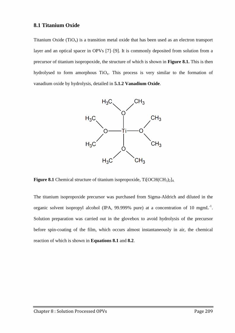
Chapter 8 : Solution Processed OPVs Page 209
8.1 Titanium Oxide
Titanium Oxide (TiOx) is a transition metal oxide that has been used as an electron transport
layer and an optical spacer in OPVs [7]–[9]. It is commonly deposited from solution from a
precursor of titanium isopropoxide, the structure of which is shown in Figure 8.1. This is then
hydrolysed to form amorphous TiOx. This process is very similar to the formation of
vanadium oxide by hydrolysis, detailed in 5.1.2 Vanadium Oxide.
Figure 8.1 Chemical structure of titanium isopropoxide, Ti[OCH(CH3)2]4.
The titanium isopropoxide precursor was purchased from Sigma-Aldrich and diluted in the
organic solvent isopropyl alcohol (IPA, 99.999% pure) at a concentration of 10 mgmL-1
.
Solution preparation was carried out in the glovebox to avoid hydrolysis of the precursor
before spin-coating of the film, which occurs almost instantaneously in air, the chemical
reaction of which is shown in Equations 8.1 and 8.2.

Chapter 8 : Solution Processed OPVs Page 210
Ti[OCH(CH3)2]4 + 4.H2O → 4.C3H7OH + Ti(OH)4 Equation 8.1
Ti(OH)4 → TiO2 + 2.H2O Equation 8.2
In Equation 8.1, in the presence of water vapour, H+ cations cleave the alkyl chain
(CH(CH3)) in the titanium isopropoxide precursor and bind to the singly bound oxygen on the
titanium oxide, forming Ti(OH)4. OH- anions bind to the alkyl chain and produce isopropanol
(C3H7OH), which evaporates. In Equation 8.2, the titanium intermediary molecules
(Ti(OH)4) react together, releasing water and form titanium oxide (TiO2). However, due to the
amorphous nature of the film, the oxidation state is likely to be less than TiO2, and therefore
the material will henceforth be referred to as TiOx.
The titanium oxide precursor solution was spin-coated at 2000 rpm to form ~ 20 nm thick
films as measured by a profilometer. These were left in air for 5 minutes to allow for the
hydrolysis process to complete fully and form an amorphous and extremely smooth TiOx
layer. The films were not annealed, as it was found to result in devices having lower
efficiency.
8.2 Solution Processed Devices
The development of methods and materials that allow high efficiency and stable devices to be
fabricated using commercial deposition techniques, such as R2R printing and spray coating, is
a key target for OPV manufacture. Vacuum deposition of materials is less attractive for
commercial production of OPVs as the process is very energy intensive [14], and thus
solution based processes offer distinct advantages. The most successful demonstration of this
technology to date was carried out by Krebs et al [15]. Multi-layer OPVs based on an inverted
Chapter 8 : Solution Processed OPVs Page 211
ITO/ZnO/P3HT:PCBM/PEDOT:PSS/Ag architecture were fabricated in one continuous
process onto a flexible poly(ethyleneterephthalate) (PET) sheet, with all layers deposited
using solution based techniques, and efficiencies of 2.3% achieved
Here, OPV devices were fabricated whose HTL, active layer, and ETL were all spin-coated
from solution with the architecture: ITO/PEDOT:PSS(30nm)/PFDT2BT-
8:PC70BM(70nm)/TiOx(20nm)/Al(100nm). The ITO anode was deposited by sputtering, and
the aluminium top cathode thermally evaporated, as no solution based deposition methods
were available. The devices were fabricated in both the glovebox and in air in the Lamarflo
work station, and several types of devices were fabricated to isolate the effects on device
performance of spin-coating the different layers in air. The active layers and TiOx ETLs were
either spin coated in air or in the glovebox, resulting in four device types: 'Fully Glovebox
Processed', 'Active Layer Glovebox, TiOx Air', 'Active Layer Air, TiOx Glovebox' and 'Fully
Air Processed'. In all cases the active layer and TiOx layer for each device were spun
sequentially, with a 30s spin time for each layer and with no delay in between depositions.
This was done to minimize the air exposure of the active layer for air processed devices, and
to emulate the fast deposition times that would be used in a commercial environment. Due to
the orthogonal nature of the solvents used, there were no issues with films being re-dissolved
by subsequent depositions. For all devices, the PEDOT:PSS HTL was spin-coated and then
only annealed in air.
Average device operating parameters are shown in Table 8.1 and JV curves in Figure 8.2.
The data represents 12 pixels across three substrates where the worst 25% of pixels have been
removed to account for gross film defect. The error quoted on all measurements is based on
the standard deviation around the mean.
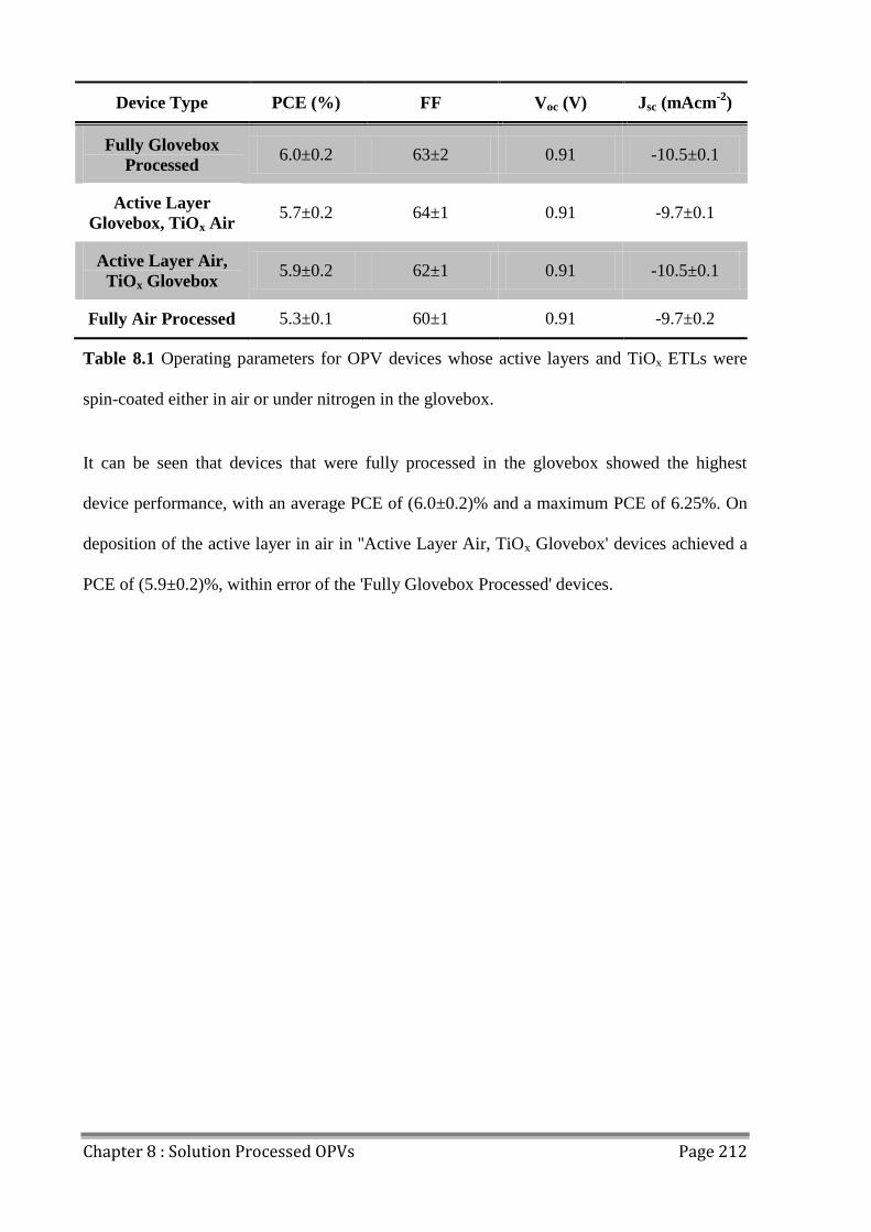
Chapter 8 : Solution Processed OPVs Page 212
Device Type PCE (%) FF Voc (V) Jsc (mAcm-2
)
Fully Glovebox
Processed 6.0±0.2 63±2 0.91 -10.5±0.1
Active Layer
Glovebox, TiOx Air 5.7±0.2 64±1 0.91 -9.7±0.1
Active Layer Air,
TiOx Glovebox 5.9±0.2 62±1 0.91 -10.5±0.1
Fully Air Processed 5.3±0.1 60±1 0.91 -9.7±0.2
Table 8.1 Operating parameters for OPV devices whose active layers and TiOx ETLs were
spin-coated either in air or under nitrogen in the glovebox.
It can be seen that devices that were fully processed in the glovebox showed the highest
device performance, with an average PCE of (6.0±0.2)% and a maximum PCE of 6.25%. On
deposition of the active layer in air in ''Active Layer Air, TiOx Glovebox' devices achieved a
PCE of (5.9±0.2)%, within error of the 'Fully Glovebox Processed' devices.
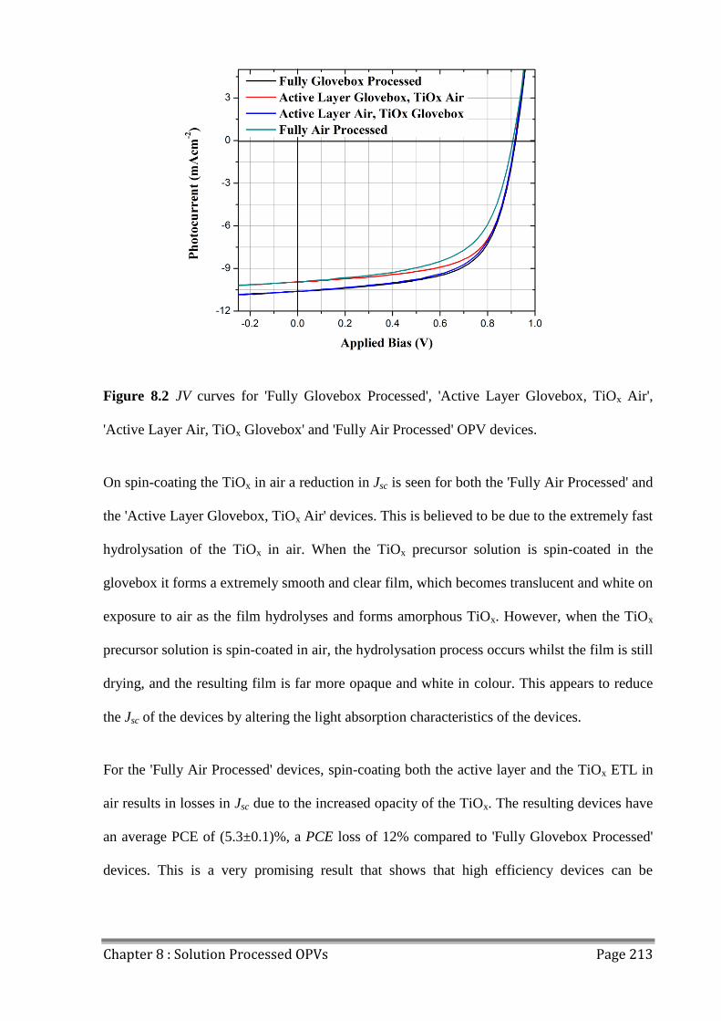
Chapter 8 : Solution Processed OPVs Page 213
Figure 8.2 JV curves for 'Fully Glovebox Processed', 'Active Layer Glovebox, TiOx Air',
'Active Layer Air, TiOx Glovebox' and 'Fully Air Processed' OPV devices.
On spin-coating the TiOx in air a reduction in Jsc is seen for both the 'Fully Air Processed' and
the 'Active Layer Glovebox, TiOx Air' devices. This is believed to be due to the extremely fast
hydrolysation of the TiOx in air. When the TiOx precursor solution is spin-coated in the
glovebox it forms a extremely smooth and clear film, which becomes translucent and white on
exposure to air as the film hydrolyses and forms amorphous TiOx. However, when the TiOx
precursor solution is spin-coated in air, the hydrolysation process occurs whilst the film is still
drying, and the resulting film is far more opaque and white in colour. This appears to reduce
the Jsc of the devices by altering the light absorption characteristics of the devices.
For the 'Fully Air Processed' devices, spin-coating both the active layer and the TiOx ETL in
air results in losses in Jsc due to the increased opacity of the TiOx. The resulting devices have
an average PCE of (5.3±0.1)%, a PCE loss of 12% compared to 'Fully Glovebox Processed'
devices. This is a very promising result that shows that high efficiency devices can be
Chapter 8 : Solution Processed OPVs Page 214
processed in air from solution based materials with only a moderate loss in overall efficiency
compared to glovebox processed devices.
For OPV devices utilising this architecture to be completely solution processed, both the ITO
and metallic electrodes, which are currently deposited via sputtering and thermal evaporation
processes respectively, need to be replaced with solution processed alternatives.
The deposition of ITO is a costly process, both due to the scarcity of indium and the energy
intensive nature of sputtering techniques, and thermal evaporation of metallic electrodes has
been shown to account for ~ 30% of energy input in the fabrication of OPV devices [14].
Solution processed alternatives to ITO include high conductivity PEDOT:PSS [16] and silver
nanowires [17], with life-cycle analyses of these materials showing a potential reduction in
module costs of up to 17% [18]. Screen printing [15], [19] and stamp-transfer [20] have been
used to successfully replace thermal evaporation for top metal contacts in R2R manufacture.
Inclusion of these materials and processes in the devices fabricated in this chapter could yield
high efficiency, low cost and air processable OPV modules compatible with R2R
manufacturing processes. However, the effects of these materials and processes on device
lifetime are as yet unknown.
Chapter 8 : Solution Processed OPVs Page 215
8.3 Conclusions
In summary, the optimisation of a solution processed OPV device that utilised a PEDOT:PSS
HTL, a PFDT2BT-8:PC70BM active layer and a TiOx ETL has been explored. The effects on
device performance of processing the active layer and ETL of the devices in a nitrogen filled
glovebox or in air were studied. It was found that processing the active layer in air resulted in
minor losses in FF, commensurate with previous findings, and processing the TiOx ETL in air
resulted in a more opaque film that resulted in Jsc losses. Devices that were processed in the
glovebox had high initial PCEs of (6.0±0.2)%, whilst those processed in air had a reduced
initial efficiency of (5.3±0.1)%.
Chapter 8 : Solution Processed OPVs Page 216
8.4 References
[1] T. Yang, W. Cai, D. Qin, E. Wang, L. Lan, X. Gong, J. Peng, and Y. Cao, “Solution-
Processed Zinc Oxide Thin Film as a Buffer Layer for Polymer Solar Cells with an Inverted
Device Structure,” J. Phys. Chem. C, vol. 114, no. 14, pp. 6849–6853, 2010.
[2] S. K. Hau, H.-L. Yip, N. S. Baek, J. Zou, K. O’Malley, and A. K.-Y. Jen, “Air-stable
inverted flexible polymer solar cells using zinc oxide nanoparticles as an electron selective
layer,” Appl. Phys. Lett., vol. 92, no. 25, p. 253301, 2008.
[3] Z. Liang, Q. Zhang, O. Wiranwetchayan, J. Xi, Z. Yang, K. Park, C. Li, and G. Cao,
“Effects of the Morphology of a ZnO Buffer Layer on the Photovoltaic Performance of
Inverted Polymer Solar Cells,” Adv. Funct. Mater., vol. 22, no. 10, pp. 2194–2201, May 2012.
[4] G. Li, C.-W. Chu, V. Shrotriya, J. Huang, and Y. Yang, “Efficient inverted polymer
solar cells,” Appl. Phys. Lett., vol. 88, no. 25, p. 253503, 2006.
[5] H.-H. Liao, L.-M. Chen, Z. Xu, G. Li, and Y. Yang, “Highly efficient inverted
polymer solar cell by low temperature annealing of Cs[sub 2]CO[sub 3] interlayer,” Appl.
Phys. Lett., vol. 92, no. 17, p. 173303, 2008.
[6] Z. He, C. Zhong, S. Su, M. Xu, H. Wu, and Y. Cao, “Enhanced power-conversion
efficiency in polymer solar cells using an inverted device structure,” Nat. Photonics, vol. 6,
no. 9, pp. 593–597, Aug. 2012.
[7] S. Chambon, E. Destouesse, B. Pavageau, L. Hirsch, and G. Wantz, “Towards an
understanding of light activation processes in titanium oxide based inverted organic solar
cells,” J. Appl. Phys., vol. 112, no. 9, p. 094503, 2012.
Chapter 8 : Solution Processed OPVs Page 217
[8] C. Waldauf, M. Morana, P. Denk, P. Schilinsky, K. Coakley, S. a. Choulis, and C. J.
Brabec, “Highly efficient inverted organic photovoltaics using solution based titanium oxide
as electron selective contact,” Appl. Phys. Lett., vol. 89, no. 23, p. 233517, 2006.
[9] J. Y. Kim, S. H. Kim, H.-H. Lee, K. Lee, W. Ma, X. Gong, and A. J. Heeger, “New
Architecture for High-Efficiency Polymer Photovoltaic Cells Using Solution-Based Titanium
Oxide as an Optical Spacer,” Adv. Mater., vol. 18, no. 5, pp. 572–576, Mar. 2006.
[10] M. T. Lloyd, D. C. Olson, P. Lu, E. Fang, D. L. Moore, M. S. White, M. O. Reese, D.
S. Ginley, and J. W. P. Hsu, “Impact of contact evolution on the shelf life of organic solar
cells,” J. Mater. Chem., vol. 19, no. 41, p. 7638, 2009.
[11] B. O’Regan and M. Gratzel, “A low-cost, high-efficiency solar cell based on dye-
sensitized colloidal TiO2 films,” Nature, vol. 353, no. 6346, pp. 737–740, Oct. 1991.
[12] U. Bach, D. Lupo, P. Comte, J. E. Moser, F. Weissortel, J. Salbeck, H. Spreitzer, and
M. Gratzel, “Solid-state dye-sensitized mesoporous TiO2 solar cells with high photon-to-
electron conversion efficiencies,” Nature, vol. 395, no. 6702, pp. 583–585, Oct. 1998.
[13] J. R. Durrant, J. Nelson, and D. R. Klug, “Functionalising nanocrystalline TiO2 films:
dye sensitised solar cells and optical biosensors,” Materials Science and Technology, vol. 16,
no. December. pp. 1345–1348, 2000.
[14] R. García-Valverde, J. a. Cherni, and A. Urbina, “Life cycle analysis of organic
photovoltaic technologies,” Prog. Photovoltaics Res. Appl., vol. 18, no. April, pp. 535–538,
2010.
Chapter 8 : Solution Processed OPVs Page 218
[15] F. C. Krebs, S. A. Gevorgyan, and J. Alstrup, “A roll-to-roll process to flexible
polymer solar cells: model studies, manufacture and operational stability studies,” J. Mater.
Chem., vol. 19, no. 30, p. 5442, 2009.
[16] S. I. Na, B. K. Yu, S. S. Kim, D. Vak, T. S. Kim, J. S. Yeo, and D. Y. Kim, “Fully
spray-coated ITO-free organic solar cells for low-cost power generation,” Sol. Energy Mater.
Sol. Cells, vol. 94, no. 8, pp. 1333–1337, 2010.
[17] D.-S. Leem, A. Edwards, M. Faist, J. Nelson, D. D. C. Bradley, and J. C. de Mello,
“Efficient organic solar cells with solution-processed silver nanowire electrodes.,” Adv.
Mater., vol. 23, no. 38, pp. 4371–5, Oct. 2011.
[18] C. J. M. Emmott, A. Urbina, and J. Nelson, “Environmental and economic assessment
of ITO-free electrodes for organic solar cells,” Sol. Energy Mater. Sol. Cells, vol. 97, pp. 14–
21, Feb. 2012.
[19] D. Angmo, T. T. Larsen-olsen, and F. C. Krebs, “Roll-to-roll fabrication of polymer
solar cells As the performance in terms of power conversion efficiency and operational,”
Mater. Today, vol. 15, no. 1, pp. 36–49, 2012.
[20] X. Wang, T. Ishwara, W. Gong, M. Campoy-Quiles, J. Nelson, and D. D. C. Bradley,
“High-performance metal-free solar cells using stamp transfer printed vapor phase
polymerized poly(3,4-ethylenedioxythiophene) top anodes,” Adv. Funct. Mater., vol. 22, pp.
1454–1460, 2012.

Chapter 9 : Conclusions Page 219
Chapter 9 : Conclusions
9.0 Conclusions of Work Undertaken
The development of R2R processing of organic photovoltaics has opened up the possibility of
commercial scale production, with printing speeds of several kilometres an hour possible
using existing technology. Unlike many forms of inorganic PV, which need to be fabricated
onto ultra-pure crystalline substrates, OPVs can be fabricated onto amorphous substrate
materials, including flexible plastics such as PET [1], [2]. This not only lowers the costs of
manufacture, but also the embodied energy cost of the devices themselves.
However, although the printing technology is available, and several pilot R2R studies have
produced promising results [3], [4], there are several challenges inherent in OPV technology
that will need to be overcome before commercialization is possible. Low efficiencies and
operating lifetimes, in comparison to the more established inorganic photovoltaic
technologies, are issues that can only partially be compensated for by lower manufacturing
costs and embodied energy.
Improvements in initial device efficiencies have been achieved with the introduction of a new
generation of donor polymers, such as PCDTBT, with low lying HOMO levels [5]. Studies
have explored PCDTBT device stability and degradation pathways [6]–[8] and have
concluded that polycarbazole polymers have a high degree of photostability [9], and can be
used to create devices having extended operational lifetimes [6]. However, the stability of
OPV devices is limited by the oxygen and moisture sensitivity of the materials used. To
overcome this, oxygen and moisture free manufacturing environments such as gloveboxes,
Chapter 9 : Conclusions Page 220
and high-grade encapsulation systems with very low moisture and oxygen ingress rates are
often used. Unfortunately, these manufacturing processes are expensive and energy intensive,
and alternatives need to be found to allow for OPV technology to be financially competitive
with silicon PV.
Throughout this work, the overarching theme was the study of OPV materials with the aim of
processing in air with little or no reduction in initial efficiency and operating lifetime. Both
active layer materials and interlayer materials were studied in detail, with the aim of
identifying materials that are air stable and result in high efficiency devices with long
operating lifetimes.
In Chapter 4, the effects on OPV device performance of exposure of MoOx HTLs to air was
studied. Ellipsometry measurements showed that air exposure resulted in a swelling of the
MoOx films on adsorption of water that was detrimental to device efficiency. However by
applying an initial thermal anneal to the MoOx film, this uptake of water could be partially
suppressed; a process that was shown to result from film densification. This result was then
used to fabricate OPV devices based on a blend of PCDTBT:PC70BM, with the active
semiconductor layer spin cast in air. Such air-processed devices had an average value for PCE
that was significantly larger than that of devices that were fabricated inside a nitrogen-filled
glovebox. This promising result suggested that the active layers of a polymer photovoltaic
device could be fabricated using an air-based processing route. These results were used in
later chapters to investigate the air stability of various donor polymers and the operational
lifetime of devices with different HTLs.
Chapter 9 : Conclusions Page 221
Chapter 5 presented a study of the operational lifetime of OPV devices utilising three
different HTL materials; MoOx, PEDOT:PSS and V2Ox. The OPV devices were tested using a
laboratory weathering test conforming to the ISOS-L-1 testing standards [10] for 620 hours of
constant illumination. It was shown that OPV devices utilising a PEDOT:PSS HTL had
higher stability than comparable devices using a MoOx or V2Ox HTLs, with extrapolated T80
lifetimes for devices utilising a PEDOT:PSS HTL being 14,500 hours (comparable to 7.2
years of outdoor use). These experiments demonstrated that the rate of degradation of the
device metrics is a significant function of the nature of the HTL material; a result that
confirms that degradation in the active layer does not completely account for the observed
reduction in device performance. Rather, the changes in FF, Jsc, and Voc that were observed
during both burn-in and subsequent linear decay must also result from the formation of
additional trap states at the interface between the active layer and the hole transport layers,
due to generation of structural and electronic defects [7], as shown in both LBIC and ELM
images of the devices after ageing. The identification of PEDOT:PSS as a stable HTL
material was key to the work in the following chapters.
In Chapter 6, five donor polymer materials were used to study the effects of air processing on
initial device efficiency. The results suggest that carbazole and fluorene based conjugated
polymers have a relatively high degree of photostability that permit them to be processed (in a
polymer:fullerene blend) into the active layer of a photovoltaic device in air with little loss in
PCE. Indeed, in some cases, devices processed in air had an enhanced efficiency compared
with comparable devices processed under nitrogen; an affect that was attributed to changes in
the work function of the underlying PEDOT:PSS anode. It was hypothesised however that the
absorption of a small quantity of water by the PEDOT:PSS anode may result in reduced
operational stability of devices over extended time periods. In addition, PFDT2BT-8:PC70BM
active layers were shown to be stable in air for up to 5 minutes during the device run with

Chapter 9 : Conclusions Page 222
little loss in device performance. This timeframe is commensurate with processing timeframes
for R2R processing, indicating that PFDT2BT-8 is a promising polymer for such
manufacturing processes.
In Chapter 7, the stability and degradation of OPV devices when tested outdoors under
conditions closely modelled on the ISOS-O-2 outdoor test were studied. The effects of daily
and seasonal light intensity and temperature variation on device performance were
investigated, and were shown to have a marked effect on the measurement of device JV
characteristics. The effects of daily fluctuations in light intensity on JV characteristics were
observed, and it was shown that FF and Voc are largely independent, though Jsc is extremely
dependent on light intensity. T80 lifetimes of ~ 2500 hours were calculated, however, it is
clear that more data recorded over a longer period is required to remove JV measurement bias
introduced by seasonal variation in temperature.
In the final results section of this thesis, Chapter 8, the optimisation of a solution processed
OPV device that utilised a PEDOT:PSS HTL, a PFDT2BT-8:PC70BM active layer and a TiOx
ETL was explored. The effects on device performance of processing the active layer and ETL
of the devices in the glovebox or in air were studied. It was found that processing the active
layer in air resulted in minor losses in FF, commensurate with previous findings, with
processing the TiOx ETL in air resulting in a more opaque film that resulted in Jsc losses.
Devices that were processed in the glovebox had high initial PCEs of (6.0±0.2)%, whilst
those processed in air had a reduced initial efficiency of (5.3±0.1)%. This promising result
suggests that it is possible to achieve high initial efficiencies for OPV devices whose active
layers and interlayers have been processed from solution in air - a key requirement for R2R
processing.
Chapter 9 : Conclusions Page 223
9.1 Suggestions for Further Work
The work presented in this thesis provides some insight into the suitability of several
commonly used OPV materials to be processed in air into devices having long operating
lifetimes. However, additional work is required to further the understanding of the
mechanisms of some of the effects observed.
In Chapter 4, the effects of thermal annealing treatments and air exposure on MoOx were
discussed. Obtaining valid XPS and UPS results would also shed light on the mechanism that
causes the change in device performance, and how adsorbed moisture affects the structure,
stoichiometry, and energy levels of MoOx. Performing lifetime tests on OPV devices whose
MoOx HTLs had undergone different thermal treatments and air exposure protocols would
shed light on the effects of air exposure and adsorbed moisture on device lifetime. Other
forms of MoOx would also benefit from study, as several solution based processing methods
have been developed for this material [11]–[14], which would be more compatible with
commercial fabrication processes.
For the lifetime study reported in Chapters 5, the degradation processes caused by the
different HTL materials warrant a detailed investigation to identify the underlying
mechanisms. This could be achieved by characterisation using LBIC and ELM imaging both
before, during and after lifetime testing. Other techniques, such as FIB/TEM cross sections of
devices could be used to identify and track the formation of defects. The understanding and
minimising the causes of device degradation is imperative for the development of
commercially viable devices with long operating lifetimes.
Chapter 9 : Conclusions Page 224
In Chapter 6, identifying the mechanism by which the polymers are oxygen doped under
illumination would allow for the design of new polymers specifically designed to be air stable
and appropriate for use in R2R fabrication.
The ongoing outdoor lifetime study detailed in Chapter 7 is planned to continue until August
2015, at which point it will be possible to extrapolate device lifetime without complicating
temperature effects. Outdoor studies are key to the understanding the real world stability of
OPVs, as our measurements using conventional solar simulators indicate that additional
degradation pathways result from fluctuations in temperature and light intensity.
A natural progression of the research presented in this thesis is the development of fully air
and solution processed devices. In Chapter 8, devices whose HTL, ETL and active layer
were all solution processed in air were fabricated and achieved a high PCE of > 5%.
However, the use of an isopropoxide precursor for the TiOx is likely to be a cause of device
stability issues, due to the action of the precursor material on the active layer causing damage
and leading to device degradation [15]. A detailed lifetime study of these devices is needed to
identify the sensitivity of the polymer to the precursor material, and if appropriate identify
other synthetic techniques to produce TiOx ETL layers that do not impact on device stability.
In addition to this, the development of solution processed anode and cathode materials is
needed to allow for devices to be processed entirely from solution, and therefore be
compatible with R2R (a result demonstrated in other studies [3], [16] using screen printing
techniques). Preliminary experiments were carried out investigating a solution processable
aluminium nano-particle suspension deposited by spray coating. However, the solvents used
in the suspension were not compatible with the underlying materials, and dissolved the entire
structure.

Chapter 9 : Conclusions Page 225
9.2 References
[1] S. R. Dupont, M. Oliver, F. C. Krebs, and R. H. Dauskardt, “Interlayer adhesion in
roll-to-roll processed flexible inverted polymer solar cells,” Sol. Energy Mater. Sol. Cells, vol.
97, pp. 171–175, Feb. 2012.
[2] G. Terán-Escobar, J. Pampel, J. M. Caicedo, and M. Lira-Cantú, “Low-temperature,
solution-processed, layered V2O5 hydrate as the hole-transport layer for stable organic solar
cells,” Energy Environ. Sci., vol. 6, no. 10, p. 3088, 2013.
[3] F. C. Krebs, S. A. Gevorgyan, and J. Alstrup, “A roll-to-roll process to flexible
polymer solar cells: model studies, manufacture and operational stability studies,” J. Mater.
Chem., vol. 19, no. 30, p. 5442, 2009.
[4] D. Angmo, P. M. Sommeling, R. Gupta, M. Hösel, S. A. Gevorgyan, J. M. Kroon, G.
U. Kulkarni, and F. C. Krebs, “Outdoor Operational Stability of Indium-Free Flexible
Polymer Solar Modules Over 1 Year Studied in India, Holland, and Denmark,” Adv. Eng.
Mater., vol. 16, no. 8, pp. 976–987, Aug. 2014.
[5] N. Blouin, A. Michaud, and M. Leclerc, “A Low-Bandgap Poly(2,7-Carbazole)
Derivative for Use in High-Performance Solar Cells,” Adv. Mater., vol. 19, no. 17, pp. 2295–
2300, Sep. 2007.
[6] C. H. Peters, I. T. Sachs-Quintana, J. P. Kastrop, S. Beaupré, M. Leclerc, and M. D.
McGehee, “High Efficiency Polymer Solar Cells with Long Operating Lifetimes,” Adv.
Energy Mater., vol. 1, no. 4, pp. 491–494, Jul. 2011.

Chapter 9 : Conclusions Page 226
[7] E. Voroshazi, I. Cardinaletti, T. Conard, and B. P. Rand, “Light-Induced Degradation
of Polymer:Fullerene Photovoltaic Devices: An Intrinsic or Material-Dependent Failure
Mechanism?,” Adv. Energy Mater., Aug. 2014.
[8] C. H. Peters, I. T. Sachs-Quintana, W. R. Mateker, T. Heumueller, J. Rivnay, R.
Noriega, Z. M. Beiley, E. T. Hoke, A. Salleo, and M. D. McGehee, “The mechanism of burn-
in loss in a high efficiency polymer solar cell,” Adv. Mater., vol. 24, no. 5, pp. 663–668, Feb.
2012.
[9] E. Bovill, H. Yi, A. Iraqi, and D. G. Lidzey, “The fabrication of polyfluorene and
polycarbazole-based photovoltaic devices using an air-stable process route,” Appl. Phys. Lett.,
vol. 105, no. 22, p. 223302, Dec. 2014.
[10] M. O. Reese, S. A. Gevorgyan, M. Jørgensen, E. Bundgaard, S. R. Kurtz, D. S.
Ginley, D. C. Olson, M. T. Lloyd, P. Morvillo, E. A. Katz, A. Elschner, O. Haillant, T. R.
Currier, V. Shrotriya, M. Hermenau, M. Riede, K. R. Kirov, G. Trimmel, T. Rath, O. Inganäs,
F. Zhang, M. Andersson, K. Tvingstedt, M. Lira-Cantu, D. Laird, C. McGuiness, S. (Jimmy)
Gowrisanker, M. Pannone, M. Xiao, J. Hauch, R. Steim, D. M. DeLongchamp, R. Rösch, H.
Hoppe, N. Espinosa, A. Urbina, G. Yaman-Uzunoglu, J.-B. Bonekamp, A. J. J. M. van
Breemen, C. Girotto, E. Voroshazi, and F. C. Krebs, “Consensus stability testing protocols for
organic photovoltaic materials and devices,” Sol. Energy Mater. Sol. Cells, vol. 95, no. 5, pp.
1253–1267, May 2011.
[11] T. Stubhan, T. Ameri, M. Salinas, J. Krantz, F. Machui, M. Halik, and C. J. Brabec,
“High shunt resistance in polymer solar cells comprising a MoO[sub 3] hole extraction layer
processed from nanoparticle suspension,” Appl. Phys. Lett., vol. 98, no. 25, p. 253308, 2011.
Chapter 9 : Conclusions Page 227
[12] C. Girotto, E. Voroshazi, D. Cheyns, P. Heremans, and B. P. Rand, “Solution-
processed MoO₃ thin films as a hole-injection layer for organic solar cells.,” ACS Appl.
Mater. interfaces, vol. 3, no. 9, pp. 3244–7, 2011.
[13] F. Liu, S. Shao, X. Guo, Y. Zhao, and Z. Xie, “Efficient polymer photovoltaic cells
using solution-processed MoO3 as anode buffer layer,” Sol. Energy Mater. Sol. Cells, vol. 94,
no. 5, pp. 842–845, May 2010.
[14] S. Murase and Y. Yang, “Solution processed MoO3 interfacial layer for organic
photovoltaics prepared by a facile synthesis method.,” Adv. Mater., vol. 24, no. 18, pp. 2459–
62, May 2012.
[15] K. Zilberberg, S. Trost, J. Meyer, A. Kahn, A. Behrendt, D. Lützenkirchen-Hecht, R.
Frahm, and T. Riedl, “Inverted Organic Solar Cells with Sol-Gel Processed High Work-
Function Vanadium Oxide Hole-Extraction Layers,” Adv. Funct. Mater., vol. 21, no. 24, pp.
4776–4783, Dec. 2011.
[16] S. A. Gevorgyan, M. V. Madsen, H. F. Dam, M. Jørgensen, C. J. Fell, K. F. Anderson,
B. C. Duck, A. Mescheloff, E. A. Katz, A. Elschner, R. Roesch, H. Hoppe, M. Hermenau, M.
Riede, and F. C. Krebs, “Interlaboratory outdoor stability studies of flexible roll-to-roll coated
organic photovoltaic modules: Stability over 10,000h,” Sol. Energy Mater. Sol. Cells, vol.
116, pp. 187–196, Sep. 2013.

Page 228

Appendix Page 229
Appendix
MATLAB Code for Laboratory Lifetime Testing System
close all
clear all
clear global
clc
%%%%%%%%%%%%%%%%%%%%%%%%%%%%%%%%%%%%%%%%%%%%%%%%%%%%%%%%%%%%%%%%%%%%%%%%%%
%user variables
%%%%%%%%%%%%%%%%%%%%%%%%%%%%%%%%%%%%%%%%%%%%%%%%%%%%%%%%%%%%%%%%%%%%%%%%%%
batch='OPV140611';
base_directory='C:\Users\Lifetime Tester PC\Desktop\Users\Ed\Thesis Calibration\6 LT LT Board
K2400 Left Wall LT Computer';
%Set number of repeats (through all devices) and delay between repeats (s)
%NOTE: Measurement takes ~120s per device (normal accuracy) ~1000s for all
%8, including the time it takes to take PD and Temp measurements.
%e.g. measuring 8 devices, 30min delay between measurements = 800s delay
repeats=1; %repeated measurements of all devices that are being tested
delay_between_repeats=0; %in seconds
delay_between_devices=0; %in seconds
start_device=1; %Device number to start testing (populate board from this number)
end_device=8; %Device number to stop testing at(populate board up to this number)
start_pixel=1; %Program will start testing from this pixel
end_pixel=6; %and finish with this pixel (1-6 only)
%New sytle substrates (single anode, pixellated cathode)
%device_area=0.02606; %cm^2 - New substrate, 6 pixel 'legless' version with mask. APETURE
MASK #2!
device_area=0.0400; %cm^2 - New substrate, 6 pixel 'legless' version without mask
%Old style substrates (single cathode, pixellated cathode)
%device_area=0.0212; %cm^2 0.0212 for standard 6 pixel with aperature mask
%device_area=0.048; %cm^2 - for standard 6 pixel without apeture mask (0.048 = corrected area,
0.045 = original area)
%device_area=0.0400; %cm^2 - New substrate, 6 pixel 'legless' version without mask
%Device architecture.
%For Pixellated Cathode Substrate (new style) Board use 1 for normal and 0 for inverted
%For Pixellated Anode Substrate (old style) Board use 0 for normal and 1 for inverted
inverted1=1;
inverted2=1;
inverted3=1;

Appendix Page 230
inverted4=1;
inverted5=1;
inverted6=1;
inverted7=1;
inverted8=1;
%Device state in between measurements.
%NOTE: Only pixels selected below will be shorted
%0 = Open circuit
%1 = Short Circuit
Device1=0;
Device2=0;
Device3=0;
Device4=0;
Device5=0;
Device6=0;
Device7=0;
Device8=0;
%Pixel state in between measurements (will be the same for all devices that are shorted)
%0 = Open circuit
%1 = Short Circuit
Pixel1=0;
Pixel2=0;
Pixel3=0;
Pixel4=0;
Pixel5=0;
Pixel6=0;
high_accuracy=0; %use if you want high accuracy measurements (will take between 2x and 10x
longer)
%this will put the K2400 on autorange, increase the settle time and GPIB timeout
%Dev Number for USB Board
%dev_number='Dev1';
dev_number='LTE';
%dev_number='LTE';
%%%%%%%%%%%%%%%%%%%%%%%%%%%%%%%%%%%%%%%%%%%%%%%%%%%%%%%%%%%%%%%%%%%%%%%%%%
%%%%%%%%%%%%%%%%%%%%%%%%%%%%%%%%%%%%%%%%%%%%%%%%%%%%%%%%%%%%%%%%%%%%%%%%%%
%%%%%%%%%%%%%%%%%%%%%%%%%%%%%%%%%%%%%%%%%%%%%%%%%%%%%%%%%%%%%%%%%%%%%%%%%%
%%%%%%%%%%%%%%%%%%MATLAB SCRIPT BELOW - DO NOT EDIT%%%%%%%%%%%%%%%%%%%%%%
%%%%%%%%%%%%%%%%%%%%%%%%%%%%%%%%%%%%%%%%%%%%%%%%%%%%%%%%%%%%%%%%%%%%%%%%%%
%%%%%%%%%%%%%%%%%%%%%%%%%%%%%%%%%%%%%%%%%%%%%%%%%%%%%%%%%%%%%%%%%%%%%%%%%%
%%%%%%%%%%%%%%%%%%%%%%%%%%%%%%%%%%%%%%%%%%%%%%%%%%%%%%%%%%%%%%%%%%%%%%%%%%
%%%%%%%%%%%%%%%%%%%%%%%%%%%%%%%%%%%%%%%%%%%%%%%%%%%%%%%%%%%%%%%%%%%%%%%%%%
%set up the inverter array for either normal or inverted operation
inverter=1;
inverted_array=[inverted1,inverted2,inverted3,inverted4,inverted5,inverted6,inverted7,inverted
8];
%%%%%%%%%%%%%%%%%%%%%%%%%%%%%%%%%%%%%%%%%%%%%%%%%%%%%%%%%%%%%%%%%%%%%%%%%%
%Create Sub Directories for devices 1-8, Photodiodes and Thermometers
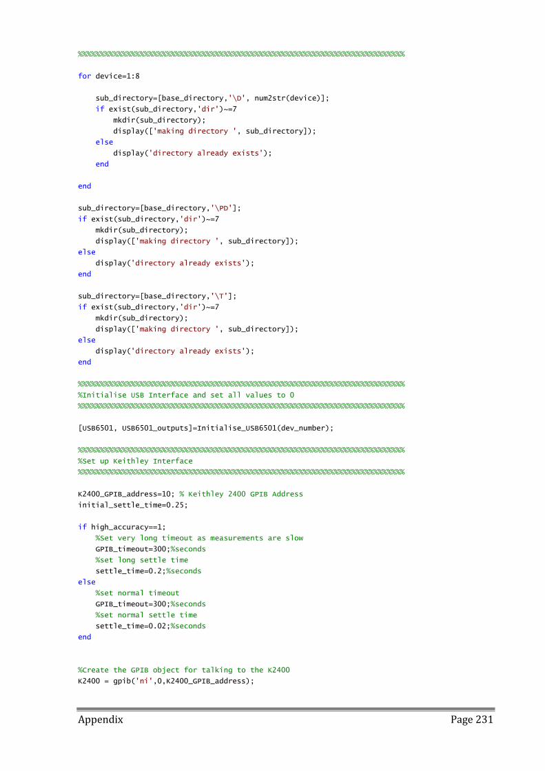
Appendix Page 231
%%%%%%%%%%%%%%%%%%%%%%%%%%%%%%%%%%%%%%%%%%%%%%%%%%%%%%%%%%%%%%%%%%%%%%%%%%
for device=1:8
sub_directory=[base_directory,'\D', num2str(device)];
if exist(sub_directory,'dir')~=7
mkdir(sub_directory);
display(['making directory ', sub_directory]);
else
display('directory already exists');
end
end
sub_directory=[base_directory,'\PD'];
if exist(sub_directory,'dir')~=7
mkdir(sub_directory);
display(['making directory ', sub_directory]);
else
display('directory already exists');
end
sub_directory=[base_directory,'\T'];
if exist(sub_directory,'dir')~=7
mkdir(sub_directory);
display(['making directory ', sub_directory]);
else
display('directory already exists');
end
%%%%%%%%%%%%%%%%%%%%%%%%%%%%%%%%%%%%%%%%%%%%%%%%%%%%%%%%%%%%%%%%%%%%%%%%%%
%Initialise USB Interface and set all values to 0
%%%%%%%%%%%%%%%%%%%%%%%%%%%%%%%%%%%%%%%%%%%%%%%%%%%%%%%%%%%%%%%%%%%%%%%%%%
[USB6501, USB6501_outputs]=Initialise_USB6501(dev_number);
%%%%%%%%%%%%%%%%%%%%%%%%%%%%%%%%%%%%%%%%%%%%%%%%%%%%%%%%%%%%%%%%%%%%%%%%%%
%Set up Keithley Interface
%%%%%%%%%%%%%%%%%%%%%%%%%%%%%%%%%%%%%%%%%%%%%%%%%%%%%%%%%%%%%%%%%%%%%%%%%%
K2400_GPIB_address=10; % Keithley 2400 GPIB Address
initial_settle_time=0.25;
if high_accuracy==1;
%Set very long timeout as measurements are slow
GPIB_timeout=300;%seconds
%set long settle time
settle_time=0.2;%seconds
else
%set normal timeout
GPIB_timeout=300;%seconds
%set normal settle time
settle_time=0.02;%seconds
end
%Create the GPIB object for talking to the K2400
K2400 = gpib('ni',0,K2400_GPIB_address);

Appendix Page 232
%set the interface mode
set(K2400,'EOSMode','read&write');
%set the end of line characters
set(K2400,'EOSCharCode','LF');
%set timeout
set(K2400,'Timeout',GPIB_timeout);
set(K2400, 'InputBufferSize', 20000);
set(K2400, 'OutputBufferSize', 20000);
%open the interface
fopen(K2400);
%Restore GPIB defaults
fprintf(K2400,':*RST')
%Clear buffer
fprintf(K2400,':TRAC:CLE')
%%%%%%%%%%%%%%%%%%%%%%%%%%%%%%%%%%%%%%%%%%%%%%%%%%%%%%%%%%%%%%%%%%%%%%%%%%
%%%%%%%%%%%%%%%%%%%%%%%%%%%%%%%%%%%%%%%%%%%%%%%%%%%%%%%%%%%%%%%%%%%%%%%%%%
%initiate all the data arrays to the correct size. This is not in general
%necessary with matlab but it does mean that we can run 1 individual pixel and the data
%formatting for the output to file remains the same which is useful.
Efficiency(6)=0;
FF(6)=0;
Jsc(6)=0;
Voc(6)=0;
max_power(6)=0;
Vmpp(6)=0;
Jmpp(6)=0;
PD(8)=0;
T(4)=0;
current_density(101,6)=0;
tic
for repeat=1:repeats
disp('********************************')
disp('********************************')
disp(['Repeat ', num2str(repeat), ' of ', num2str(repeats)] );
%%%%%%%%%%%%%%%%%%%%%%%%%%%%%%%%%%%%%%%%%%%%%%%%%%%%%%%%%%%%%%%%%%%%%%%%%%
% Photodiode and Thermometer Measurements
%%%%%%%%%%%%%%%%%%%%%%%%%%%%%%%%%%%%%%%%%%%%%%%%%%%%%%%%%%%%%%%%%%%%%%%%%%
% Restore GPIB defaults
fprintf(K2400,':*RST')
%Clear buffer
fprintf(K2400,':TRAC:CLE')
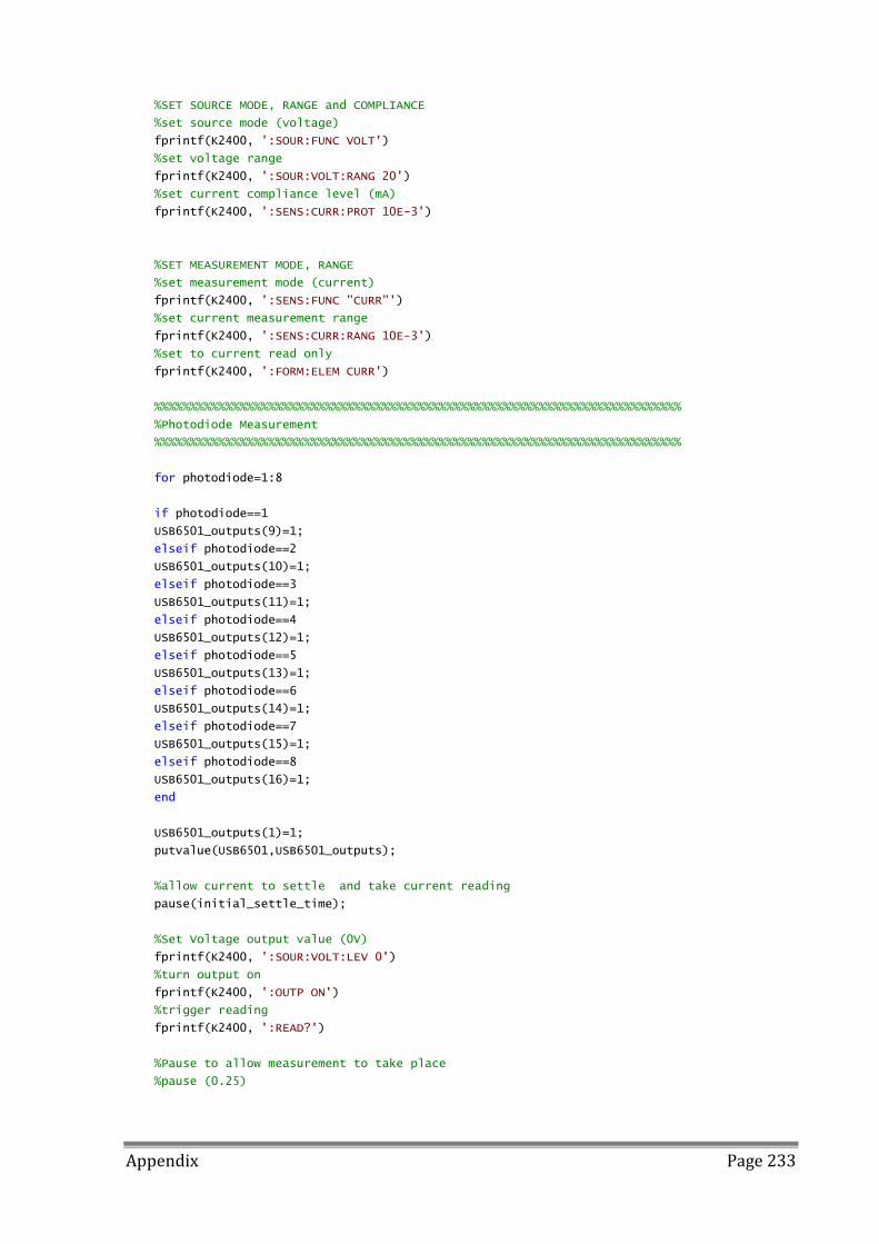
Appendix Page 233
%SET SOURCE MODE, RANGE and COMPLIANCE
%set source mode (voltage)
fprintf(K2400, ':SOUR:FUNC VOLT')
%set voltage range
fprintf(K2400, ':SOUR:VOLT:RANG 20')
%set current compliance level (mA)
fprintf(K2400, ':SENS:CURR:PROT 10E-3')
%SET MEASUREMENT MODE, RANGE
%set measurement mode (current)
fprintf(K2400, ':SENS:FUNC "CURR"')
%set current measurement range
fprintf(K2400, ':SENS:CURR:RANG 10E-3')
%set to current read only
fprintf(K2400, ':FORM:ELEM CURR')
%%%%%%%%%%%%%%%%%%%%%%%%%%%%%%%%%%%%%%%%%%%%%%%%%%%%%%%%%%%%%%%%%%%%%%%%%%
%Photodiode Measurement
%%%%%%%%%%%%%%%%%%%%%%%%%%%%%%%%%%%%%%%%%%%%%%%%%%%%%%%%%%%%%%%%%%%%%%%%%%
for photodiode=1:8
if photodiode==1
USB6501_outputs(9)=1;
elseif photodiode==2
USB6501_outputs(10)=1;
elseif photodiode==3
USB6501_outputs(11)=1;
elseif photodiode==4
USB6501_outputs(12)=1;
elseif photodiode==5
USB6501_outputs(13)=1;
elseif photodiode==6
USB6501_outputs(14)=1;
elseif photodiode==7
USB6501_outputs(15)=1;
elseif photodiode==8
USB6501_outputs(16)=1;
end
USB6501_outputs(1)=1;
putvalue(USB6501,USB6501_outputs);
%allow current to settle and take current reading
pause(initial_settle_time);
%Set Voltage output value (0V)
fprintf(K2400, ':SOUR:VOLT:LEV 0')
%turn output on
fprintf(K2400, ':OUTP ON')
%trigger reading
fprintf(K2400, ':READ?')
%Pause to allow measurement to take place
%pause (0.25)

Appendix Page 234
%read it off the GPIB
raw_data = fscanf(K2400);
% %turn output off
% fprintf(K2400, ':OUTP OFF')
%turn the text into an array of numbers
processed_data = sscanf(raw_data,'%g,');
%and pick off the measurement we want
PD(photodiode) = processed_data;
disp(['Reference photodiode ',num2str(photodiode),' current=' num2str(PD(photodiode)) ]);
USB6501_outputs=logical([0 0 0 0 0 0 0 0 0 0 0 0 0 0 0 0 0 0 0 0 0 0
0 0]);
putvalue(USB6501,USB6501_outputs);
end
%write photodiode measurements to file
directory=[base_directory,'\PD'];
fid=fopen([directory,'\PD.csv'],'a');
fprintf(fid,'PD,%g,%g,%g,%g,%g,%g,%g,%g,%g\n',toc,PD);
fclose(fid);
%%%%%%%%%%%%%%%%%%%%%%%%%%%%%%%%%%%%%%%%%%%%%%%%%%%%%%%%%%%%%%%%%%%%%%%%%%
%Thermometer Measurement
%%%%%%%%%%%%%%%%%%%%%%%%%%%%%%%%%%%%%%%%%%%%%%%%%%%%%%%%%%%%%%%%%%%%%%%%%%
for temp=1:4
if temp==1
USB6501_outputs(9)=1;
elseif temp==2
USB6501_outputs(10)=1;
elseif temp==3
USB6501_outputs(11)=1;
elseif temp==4
USB6501_outputs(12)=1;
end
USB6501_outputs(8)=1;
putvalue(USB6501,USB6501_outputs);
%allow current to settle and take current reading
pause(initial_settle_time);
%Set Voltage output value (0V)
fprintf(K2400, ':SOUR:VOLT:LEV 0')
% %turn output on
% fprintf(K2400, ':OUTP ON')
%trigger reading
fprintf(K2400, ':READ?')
%Pause to allow measurement to take place
%pause (0.25)

Appendix Page 235
%read it off the GPIB
raw_data = fscanf(K2400);
% %turn output off
% fprintf(K2400, ':OUTP OFF')
%turn the text into an array of numbers
processed_data = sscanf(raw_data,'%g,');
%and pick off the measurement we want
T(temp) = -273.15 -(1E9/227)*processed_data ;
disp(['Temperature ', num2str(temp), ' =', num2str(T(temp)) ]);
USB6501_outputs=logical([0 0 0 0 0 0 0 0 0 0 0 0 0 0 0 0 0 0 0 0 0 0
0 0]);
putvalue(USB6501,USB6501_outputs);
end
%write thermometer measurements to file
directory=[base_directory,'\T'];
fid=fopen([directory,'\T.csv'],'a');
fprintf(fid,'T,%g,%g,%g,%g,%g\n',toc,T);
fclose(fid);
%%%%%%%%%%%%%%%%%%%%%%%%%%%%%%%%%%%%%%%%%%%%%%%%%%%%%%%%%%%%%%%%%%%%%%%%%%
%Set up Keithley for JV measurement
%%%%%%%%%%%%%%%%%%%%%%%%%%%%%%%%%%%%%%%%%%%%%%%%%%%%%%%%%%%%%%%%%%%%%%%%%%
% Restore GPIB defaults
fprintf(K2400,':*RST')
%Clear and set up buffer
fprintf(K2400,':TRAC:CLE')
%set up buffer size
fprintf(K2400,':TRAC:POIN 101')
%turn off concurrent functions
fprintf(K2400,':SENS:FUNC:CONC ON')
%set up source mode (voltage)
fprintf(K2400,':SOUR:FUNC VOLT')
%set measurement mode (current)
fprintf(K2400,':SENS:FUNC "CURR"')
%set current limit
fprintf(K2400,':SENS:CURR:PROT 10E-3')
fprintf(K2400,':SENS:CURR:RANG:AUTO OFF')
%Set NPLC
fprintf(K2400,':SENS:CURR:NPLC 1');
%set voltage start
fprintf(K2400,':SOUR:VOLT:START -1')
%set voltage stop
fprintf(K2400,':SOUR:VOLT:STOP 1.0')
%set voltage step
fprintf(K2400,':SOUR:VOLT:STEP 0.02')
fprintf(K2400,':SOUR:CLE:AUTO ON')
%set voltage sweep
fprintf(K2400,':SOUR:VOLT:MODE SWE')
%set fixed range on source
fprintf(K2400,':SOUR:SWE:RANG FIX')

Appendix Page 236
%set sweep type (linear)
fprintf(K2400,':SOUR:SWE:SPAC LIN')
%trigger count (=number of sweep points = stop-start/step +1)
fprintf(K2400,':TRIG:COUNT 101')
fprintf(K2400,':TRIG:DEL 0')
%set source delay
fprintf(K2400,':SOUR:DEL 0.1')
for device=start_device:end_device
%Set the Inverter for inverted or normal devices
inverter=1;
if inverted_array(device)==1;
inverter=-1;
end
%clears figure in between devices
clf;
disp('********************************')
disp('********************************')
disp(['Testing Device #', num2str(device), ' of ', num2str([end_device-start_device+1])]
);
t=clock;
time_string=[num2str(t(1)),'.',num2str(t(2)),'.',num2str(t(3)),'
',num2str(t(4)),'.',num2str(t(5)),'.',num2str(round(t(6)))];
directory=[base_directory,'\D', num2str(device)];
file_name=[time_string,' ',num2str(batch),'-', 'Device', num2str(device), ' Repeat',
num2str(repeat),];
file_path=[directory,'\',file_name,'.csv'];
%turn off everything for safety reasons
USB6501_outputs=logical([0 0 0 0 0 0 0 0 0 0 0 0 0 0 0 0 0 0 0 0 0 0
0 0]);
putvalue(USB6501,USB6501_outputs);
if device==1
USB6501_outputs(9)=1;
elseif device==2
USB6501_outputs(10)=1;
elseif device==3
USB6501_outputs(11)=1;
elseif device==4
USB6501_outputs(12)=1;
elseif device==5
USB6501_outputs(13)=1;
elseif device==6
USB6501_outputs(14)=1;
elseif device==7
USB6501_outputs(15)=1;
elseif device==8

Appendix Page 237
USB6501_outputs(16)=1;
end
for pixel= start_pixel:end_pixel
%Clear buffer
fprintf(K2400,':DATA:CLE')
%enable buffer
fprintf(K2400,':TRAC:FEED:CONT NEXT')
%debugging point 2
%disp(['DP2', ' Rep=',num2str(repeat),' Dev=',num2str(repeat),'
Pix=',num2str(pixel), ' Inverter=', num2str(inverter)]);
if pixel==1;
USB6501_outputs(2)=1;
elseif pixel==2
USB6501_outputs(3)=1;
elseif pixel==3
USB6501_outputs(4)=1;
elseif pixel==4
USB6501_outputs(5)=1;
elseif pixel==5
USB6501_outputs(6)=1;
elseif pixel==6
USB6501_outputs(7)=1;
end
%Switch on pixel by sending value to board
putvalue(USB6501,USB6501_outputs);
pause(0.5);
%Display: Device X Pixel X on
disp(['********************************'])
disp(['Device ',num2str(device),' Pixel ',num2str(pixel),' on'])
%Pause if necessary
pause(initial_settle_time);
%Initiate readings
fprintf(K2400,':INIT')
disp('Reading Currents')
%Pause to allow measurement to take place ~7s
%pause (7)
%Recall data from buffer (voltage,current,time,resistance,?)
fprintf(K2400,':TRAC:DATA?');
%Turn huge data string into numbers
raw_data=str2num(fscanf(K2400));
%Pick out data we want
voltage=inverter * raw_data(1:5:505)';
current=inverter * raw_data(2:5:505)';

Appendix Page 238
%flip data if inverter=-1 to make sure Voc is correctly calculated
if inverter==-1;
voltage=flipud(voltage);
current=flipud(current);
end
current_density(:,pixel)=1000*current/device_area;
%Switch off pixel
USB6501_outputs(pixel+1)=0;
putvalue(USB6501,USB6501_outputs);
disp('Plotting')
plot(voltage,current_density(:,pixel)); grid on; hold on;
disp('Calculating key parameters')
%calculate key parameters
power=abs(voltage.*current); %Watts
%find key parameters
max_power(pixel)=0;
max_power_data_point=1;
Jsc(pixel)=0;
Voc(pixel)=0;
for i=1:1:101
if voltage(i)==0;
Jsc(pixel)=current_density(i,pixel);
end
if voltage(i) > 0 && current(i) <= 0 && i<101
Voc(pixel)= voltage(i) + (0-current(i)) * (voltage(i+1)-voltage(i)) /
(current(i+1)-current(i)) ;
if power(i)>=max_power(pixel);
max_power_data_point=i;
max_power(pixel)=power(i);
end
end
end
Vmpp(pixel)=voltage(max_power_data_point);
Jmpp(pixel)=current_density(max_power_data_point,pixel);
%disp(['Vmpp=',num2str(Vmpp(pixel))]);
%disp(['Jmpp=',num2str(Jmpp(pixel))]);
%calculate efficiency from the maximum output power divided by the input
%power of the device area times the solar power density
%(1000 watts/m^2 = 0.1 %W/cm^2)
%x100 to turn into percent
Efficiency(pixel)=100*max_power(pixel)/(device_area*0.1);
FF(pixel)=100*Vmpp(pixel)*Jmpp(pixel)/(Voc(pixel)*Jsc(pixel));
disp(['PCE=',num2str(Efficiency(pixel)),' Jsc=',num2str(Jsc(pixel)),'
Voc=',num2str(Voc(pixel)),' FF=',num2str(FF(pixel))]);
%%%%%%%%%%%%%%%%%%%%%%%%%%%%%%%%%%%%%%%%%%%%%%%%%%%%%

Appendix Page 239
%write JV data to file for this device in the device subdirectory
%write data file for this device
fid=fopen(file_path,'w');
fprintf(fid,'Bias,J(pixel 1),J(pixel 2),J(pixel 3),J(pixel 4),J(pixel 5),J(pixel
6)\n');
fprintf(fid,'V,mA/cm^2,mA/cm^2,mA/cm^2,mA/cm^2,mA/cm^2,mA/cm^2\n');
fprintf(fid,'%g,%g,%g,%g,%g,%g,%g\n', [voltage ,current_density].');
fprintf(fid,'\n\n');
fprintf(fid,'Parameter,Pixel 1,Pixel 2,Pixel 3,Pixel 4,Pixel 5,Pixel 6\n');
fprintf(fid,'Voc (V),%g,%g,%g,%g,%g,%g\n',Voc);
fprintf(fid,'Jsc (mA/cm^2),%g,%g,%g,%g,%g,%g\n',Jsc);
fprintf(fid,'FF (%%),%g,%g,%g,%g,%g,%g\n',FF);
fprintf(fid,'Vmpp (V),%g,%g,%g,%g,%g,%g\n',Vmpp);
fprintf(fid,'Jmpp (mA/cm^2),%g,%g,%g,%g,%g,%g\n',Jmpp);
fprintf(fid,'Efficiency (%%),%g,%g,%g,%g,%g,%g\n',Efficiency);
fprintf(fid,'\n\n');
fprintf(fid,'\nDevice Area,%g,cm^2',device_area);
fprintf(fid,'\nsettle_time,%g,seconds',settle_time);
fclose(fid);
%disable buffer - needs to be done so the buffer can be
%cleared before the next reading is taken.
fprintf(K2400,':TRAC:FEED:CONT NEV')
end
%Append data to summary files for this device in the device subdirectory
%for Voc
fid=fopen([directory,'\Voc.csv'],'a');
fprintf(fid,'%s,%s,%s,%g,%g,%g,%g,%g,%g,%g\n',time_string,batch,['D',num2str(device)],toc,Voc)
;
fclose(fid);
%for Jsc
fid=fopen([directory,'\Jsc.csv'],'a');
fprintf(fid,'%s,%s,%s,%g,%g,%g,%g,%g,%g,%g\n',time_string,batch,['D',num2str(device)],toc,Jsc)
;
fclose(fid);
%for FF
fid=fopen([directory,'\FF.csv'],'a');
fprintf(fid,'%s,%s,%s,%g,%g,%g,%g,%g,%g,%g\n',time_string,batch,['D',num2str(device)],toc,FF);
fclose(fid);
%for PCE
fid=fopen([directory,'\PCE.csv'],'a');
fprintf(fid,'%s,%s,%s,%g,%g,%g,%g,%g,%g,%g\n',time_string,batch,['D',num2str(device)],toc,Effi
ciency);
Appendix Page 240
fclose(fid);
%for Vmpp
fid=fopen([directory,'\VMPP.csv'],'a');
fprintf(fid,'%s,%s,%s,%g,%g,%g,%g,%g,%g,%g\n',time_string,batch,['D',num2str(device)],toc,Vmpp
);
fclose(fid);
%for Jmpp
fid=fopen([directory,'\JMPP.csv'],'a');
fprintf(fid,'%s,%s,%s,%g,%g,%g,%g,%g,%g,%g\n',time_string,batch,['D',num2str(device)],toc,Jmpp
);
fclose(fid);
pause(delay_between_devices);
end
%%%%%%%%%%%%%%%%%%%%%%%%%%%%%%%%%%%%%%%%%%%%%%%%%%%%%%%%%%%%%%%%%%%%%%%%%%
%Set devices in open or short circuit after measurements
%%%%%%%%%%%%%%%%%%%%%%%%%%%%%%%%%%%%%%%%%%%%%%%%%%%%%%%%%%%%%%%%%%%%%%%%%%
USB6501_outputs=logical([0 Pixel1 Pixel2 Pixel3 Pixel4 Pixel5 Pixel6 0 Device1
Device2 Device3 Device4 Device5 Device6 Device7 Device8 1 0 0 0 0 0 0 0]);
putvalue(USB6501,USB6501_outputs);
pause(delay_between_repeats);
end
%turn everything off
USB6501_outputs=logical([0 0 0 0 0 0 0 0 0 0 0 0 0 0 0 0 0 0 0 0 0 0 0
0]);
putvalue(USB6501,USB6501_outputs);
%turn output off
fprintf(K2400, ':OUTP OFF')
%close down instruments
% Restore GPIB defaults
fprintf(K2400,':*RST')
fprintf(K2400,':*CLS ')
fprintf(K2400,':*SRE 0');
delete(USB6501); clear USB6501;
%delete GPIB objects
fclose(K2400);delete(K2400);clear K2400;


![11.[70-87]Operational Diversification and Stability of Financial Performance in Indian Banking Sector](https://img.pdfslide.net/doc/110x75/577d1e5a1a28ab4e1e8e5585/1170-87operational-diversification-and-stability-of-financial-performance.jpg)