Embed Size (px)
Citation preview

The “Ground” MythBruce Archambeault, Ph.D.
IBM Distinguished Engineer, IEEE [email protected]
18 November 2008
IEEE

November 2008 Bruce Archambeault, PhD 2
Introduction
• Electromagnetics can be scary– Universities LOVE messy math
• EM is not hard, unless you want to do the messy math
• Goal:– Intuitive understanding– Understand the basic fundamentals – Understand how to read the math
November 2008 Bruce Archambeault, PhD 3

November 2008 Bruce Archambeault, PhD 4
Overview
• What does the derivative mean?• What does integration mean?• Weird vector notation• In the beginning – Faraday and Maxwell• Inductance• “Ground”• Primary cause of EMI problems on
PCBs

November 2008 Bruce Archambeault, PhD 5
Derivative
• How fast is somethingchanging?
[ ]somethingdtd Changing with
respect to time
[ ]somethingdxd Changing with respect
to position (x)

November 2008 Bruce Archambeault, PhD 6
Partial Derivative
• How fast is something changing for one variable?
[ ]),( xtsomethingt∂∂
Changing with respect to time (as ‘x’ is constant)
Changing with respect to position (x) (as time is constant)
[ ]),( xtsomethingx∂∂
November 2008 Bruce Archambeault, PhD 7
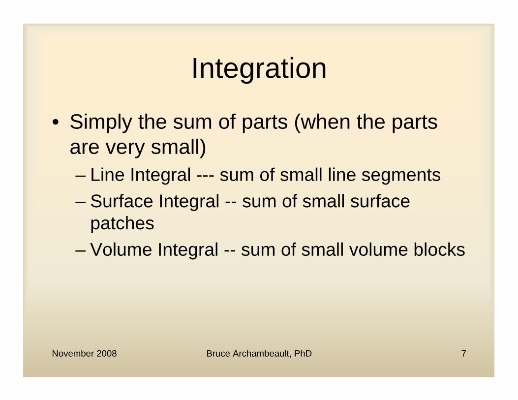
Integration
• Simply the sum of parts (when the parts are very small)– Line Integral --- sum of small line segments– Surface Integral -- sum of small surface
patches– Volume Integral -- sum of small volume blocks

November 2008 Bruce Archambeault, PhD 8
Line Integral (find the length of the path)
)( dlEVstop
start
•−=→
∫
dl
‘piece’ of E field

November 2008 Bruce Archambeault, PhD 9
Line Integral -- Closed
∫= boxaroundpathnceCircumfere
x
y
∫∫∫∫=
=
=
=
=
=
=
=
+++=00
00
y
wy
x
lx
wy
y
lx
x
dydxdydx

November 2008 Bruce Archambeault, PhD 10
Line Integral -- Closed
• Closed line integrals find the path length
• And/or the amount of some quantity along that closed path length

November 2008 Bruce Archambeault, PhD 11
Surface Integral(find the area of the surface)
∫∫
∫
∗=
∗=
=
dydxArea
dydxda
daArea
As dx and dy become smaller and smaller, the area is better calculated

November 2008 Bruce Archambeault, PhD 12
Volume Integral(find the volume of an object)
∫∫∫
∫
∗∗=
∗∗=
=
][ dzdydxVolume
dzdydxdv
dvVolume
November 2008 Bruce Archambeault, PhD 13
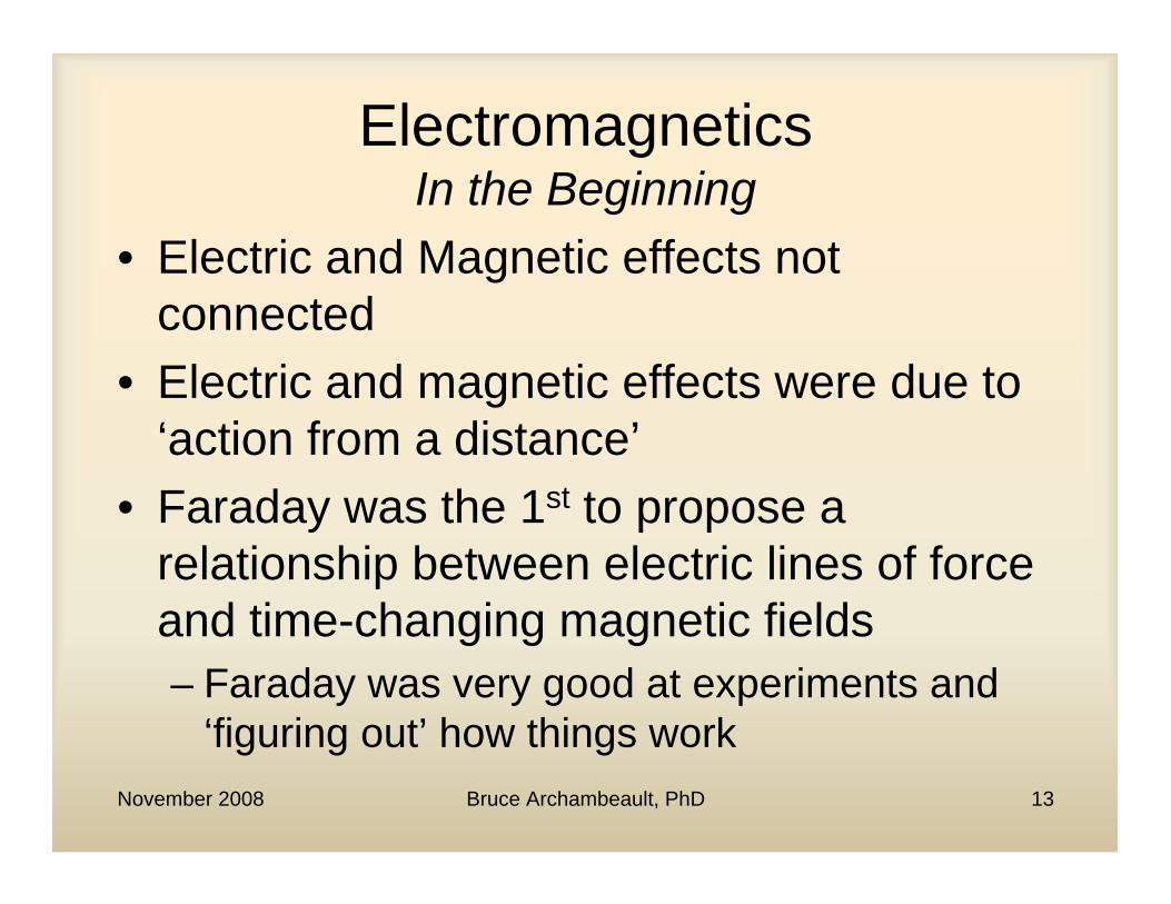
ElectromagneticsIn the Beginning
• Electric and Magnetic effects not connected
• Electric and magnetic effects were due to ‘action from a distance’
• Faraday was the 1st to propose a relationship between electric lines of force and time-changing magnetic fields– Faraday was very good at experiments and
‘figuring out’ how things work
November 2008 Bruce Archambeault, PhD 14
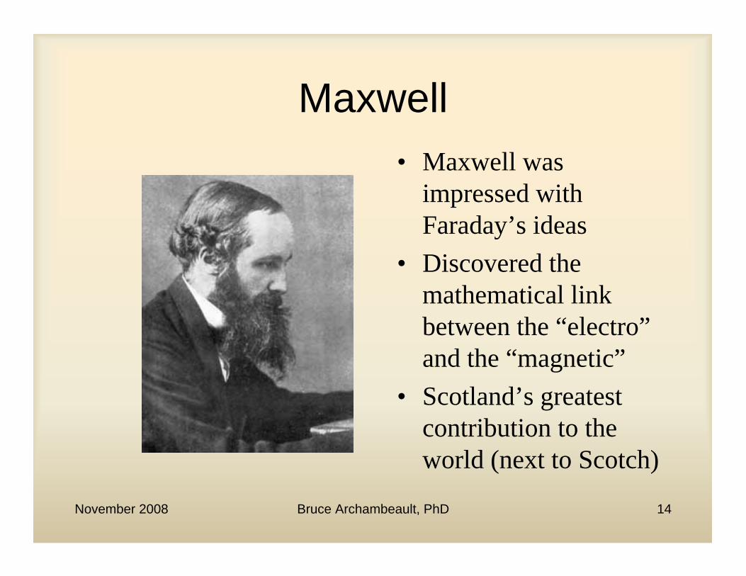
Maxwell• Maxwell was
impressed with Faraday’s ideas
• Discovered the mathematical link between the “electro” and the “magnetic”
• Scotland’s greatest contribution to the world (next to Scotch)
November 2008 Bruce Archambeault, PhD 15
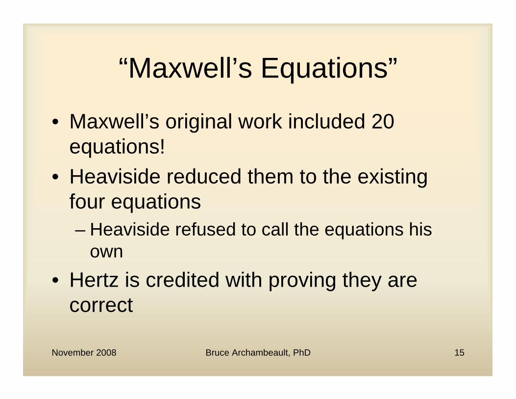
“Maxwell’s Equations”
• Maxwell’s original work included 20 equations!
• Heaviside reduced them to the existing four equations– Heaviside refused to call the equations his
own• Hertz is credited with proving they are
correct

November 2008 Bruce Archambeault, PhD 16
Maxwell’s Equations are NOT Hard!
tBE
tDJH
∂∂
∂∂
−=×∇
+=×∇
November 2008 Bruce Archambeault, PhD 17
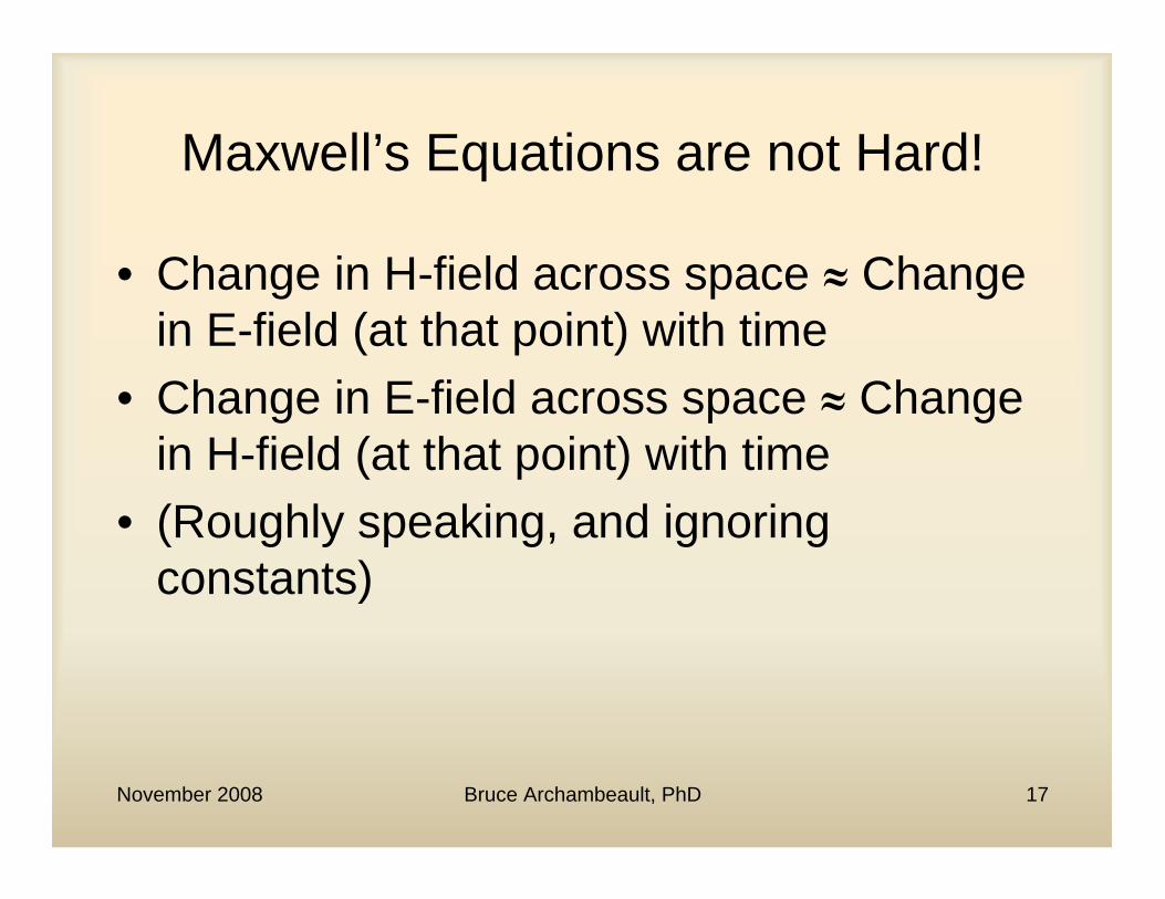
Maxwell’s Equations are not Hard!
• Change in H-field across space ¡ Change in E-field (at that point) with time
• Change in E-field across space ¡ Change in H-field (at that point) with time
• (Roughly speaking, and ignoring constants)

November 2008 Bruce Archambeault, PhD 18
Current Flow• Most important concept of EMC• Current flow through metal changes as
frequency increases• DC current
– Uses entire conductor– Only resistance inhibits current
• High Frequency– Only small part of conductor (near surface) is used– Resistance is small part of current inhibitor– Inductance is major part of current inhibitor

November 2008 Bruce Archambeault, PhD 19
Skin Depth• High frequency current flows only near the
metal surface at high frequencies
Frequency Skin Depth Skin Depth 60 Hz 260 mils 8.5 mm 1 KHz 82 mils 2.09 mm 10 KHz 26 mils 0.66 mm
100 KHz 8.2 mils 0.21 mm 1 MHz 2.6 mils 0.066 mm 10 MHz 0.82 mils 0.021 mm
100 MHz 0.26 mils 0.0066 mm 1 GHz 0.0823 mils 0.0021 mm
μσπδ
f1
=

November 2008 Bruce Archambeault, PhD 20
Inductance
• Current flow through metal => inductance!
• Fundamental element in EVERYTHING• Loop area first order concern• Inductive impedance increases with
frequency and is MAJOR concern at high frequencies
fLX L π2=

November 2008 Bruce Archambeault, PhD 21
Current Loop => Inductance
Courtesy of Elya Joffe

November 2008 Bruce Archambeault, PhD 22
Inductance Definition
• Faraday’s Law∫ ∫∫ ⋅
∂∂
−=⋅ SdtBdlE
tBAV∂∂
−=V
B
Area = A
• For a simple rectangular loop
The minus sign means that the induced voltage will work against the current that originally created the magnetic field!
November 2008 Bruce Archambeault, PhD 23
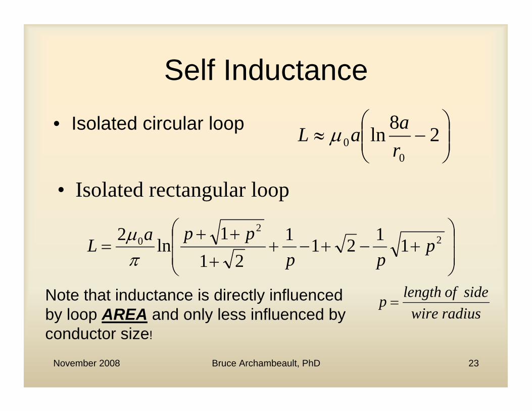
Self Inductance
• Isolated circular loop⎟⎟⎠
⎞⎜⎜⎝
⎛−≈ 28ln
00 r
aaL μ
⎟⎟
⎠
⎞
⎜⎜
⎝
⎛+−+−+
+++
= 22
0 1121121
1ln2 p
ppppaL
πμ
• Isolated rectangular loop
Note that inductance is directly influenced by loop AREA and only less influenced by conductor size!
radiuswiresideoflengthp =

November 2008 Bruce Archambeault, PhD 24
Partial Inductance
• Simply a way to break the overall loopinto pieces in order to find total inductance
L3
L4
L2
L1
L total=Lp11+ Lp22 + Lp33 + Lp44 - 2Lp13 - 2Lp24

November 2008 Bruce Archambeault, PhD 25
Important Points About Inductance
• Inductance is everywhere• Loop area most important• Inductance is everywhere

November 2008 Bruce Archambeault, PhD 26
Decoupling Capacitor Mounting
• Keep as to planes as close to capacitor pads as possible
Height above Planes
Via Separation
Inductance Depends on Loop AREA
November 2008 Bruce Archambeault, PhD 27
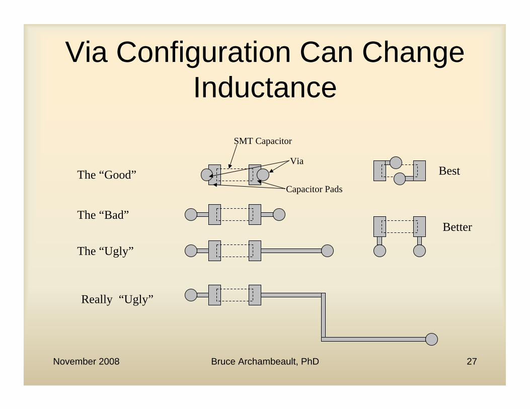
Via Configuration Can Change Inductance
Via
Capacitor Pads
SMT Capacitor
The “Good”
The “Bad”
The “Ugly”
Really “Ugly”
Better
Best

November 2008 Bruce Archambeault, PhD 28
Comparison of Decoupling Capacitor Impedance100 mil Between Vias & 10 mil to Planes
0.01
0.1
1
10
100
1000
1.0E+06 1.0E+07 1.0E+08 1.0E+09 1.0E+10
Frequency (Hz)
Impe
danc
e (o
hms)
1000pF
0.01uF
0.1uF
1.0uF

November 2008 Bruce Archambeault, PhD 29
Comparison of Decoupling Capacitor Via Separation Distance Effects
10 mils
Via Separation
0603 Typical Minimum
Dimensions
November 2008 Bruce Archambeault, PhD 30
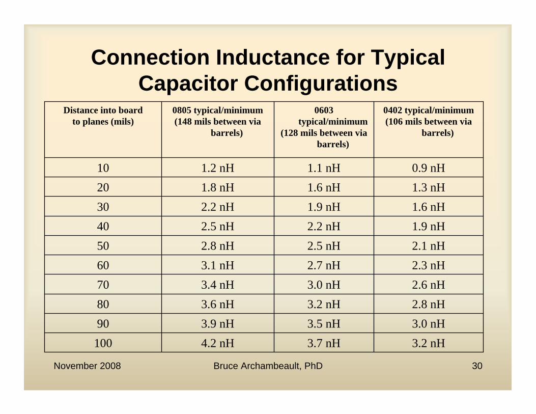
Connection Inductance for Typical Capacitor Configurations
3.2 nH3.7 nH4.2 nH1003.0 nH3.5 nH3.9 nH902.8 nH3.2 nH3.6 nH802.6 nH3.0 nH3.4 nH702.3 nH2.7 nH3.1 nH602.1 nH2.5 nH2.8 nH501.9 nH2.2 nH2.5 nH401.6 nH1.9 nH2.2 nH301.3 nH1.6 nH1.8 nH200.9 nH1.1 nH1.2 nH10
0402 typical/minimum(106 mils between via
barrels)
0603 typical/minimum
(128 mils between via barrels)
0805 typical/minimum (148 mils between via
barrels)
Distance into board to planes (mils)

November 2008 Bruce Archambeault, PhD 31
‘Ground’
• Ground is a place where potatoes and carrots thrive!
• ‘Earth’ or ‘reference’ is more descriptive • Original use of “GROUND”• Inductance is everywhere
fLX L π2=
November 2008 Bruce Archambeault, PhD 32
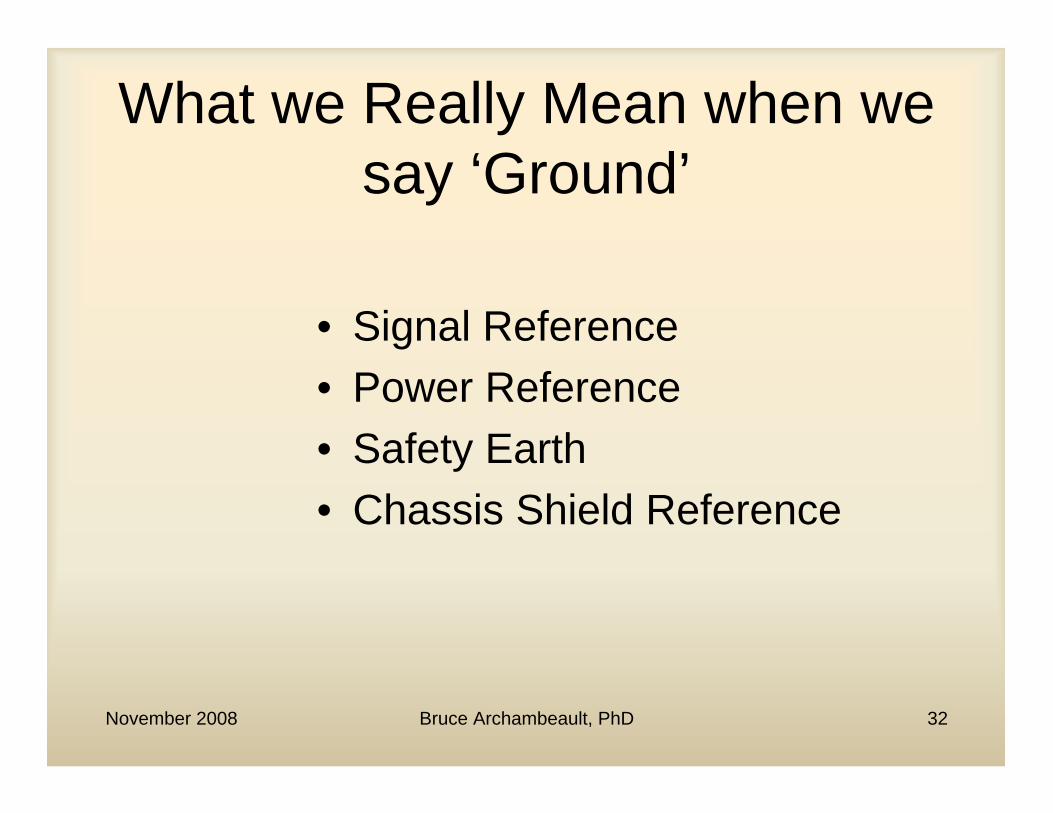
What we Really Mean when we say ‘Ground’
• Signal Reference• Power Reference• Safety Earth• Chassis Shield Reference

November 2008 Bruce Archambeault, PhD 33
‘Ground’ is NOT a Current Sink!
• Current leaves a driver on a trace and must return (somehow) to its source
• This seems basic, but it is often forgotten, and is most often the cause of EMC problems
November 2008 Bruce Archambeault, PhD 34
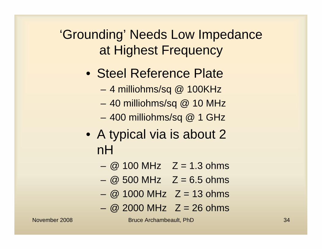
‘Grounding’ Needs Low Impedance at Highest Frequency
• Steel Reference Plate– 4 milliohms/sq @ 100KHz– 40 milliohms/sq @ 10 MHz– 400 milliohms/sq @ 1 GHz
• A typical via is about 2 nH– @ 100 MHz Z = 1.3 ohms– @ 500 MHz Z = 6.5 ohms– @ 1000 MHz Z = 13 ohms– @ 2000 MHz Z = 26 ohms

November 2008 Bruce Archambeault, PhD 35
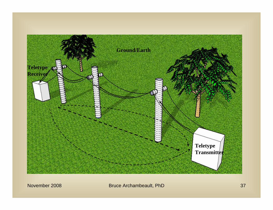
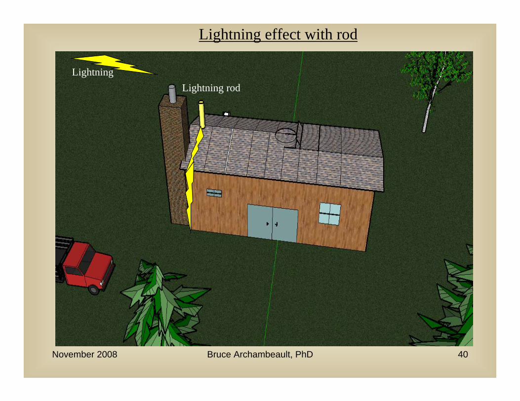
Where did the Term “GROUND” Originate?
• Original Teletype connections• Lightning Protection

November 2008 Bruce Archambeault, PhD 36
Ground/Earth
TeletypeReceiver
TeletypeTransmitter
November 2008 Bruce Archambeault, PhD 37
Ground/Earth
TeletypeReceiver
TeletypeTransmitter
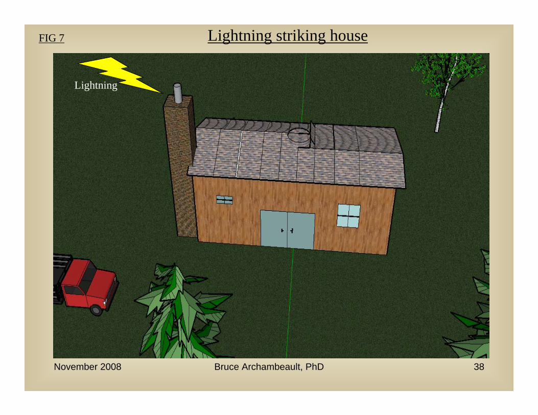
November 2008 Bruce Archambeault, PhD 38
Lightning striking houseFIG 7
Lightning

November 2008 Bruce Archambeault, PhD 39
Lightning effect without rod
November 2008 Bruce Archambeault, PhD 40
Lightning effect with rod
Lightning rodLightning

November 2008 Bruce Archambeault, PhD 41
What we Really Mean when we say ‘Ground’
• Signal Reference• Power Reference• Safety Earth• Chassis Shield Reference
Circuit “Ground”
Chassis “Ground”
Digital “Ground”
D
Analog “Ground”
A

November 2008 Bruce Archambeault, PhD 42

November 2008 Bruce Archambeault, PhD 43
Schematic with return current shown
IC1 IC2 IC3
Return currents on ground
Signal trace currents

November 2008 Bruce Archambeault, PhD 44
Actual Current Return is 3-Dimensional
Ground Layer
Signal Trace
IC
Ground Vias
Ground Layer
Signal TraceICGround Via
BOARD STACK UP:
Ground Layer
Signal TraceCURRENT LOCATION:

November 2008 Bruce Archambeault, PhD 45
Low Frequency Return Currents Take Path of Least Resistance
Ground Plane
DriverReceiver

November 2008 Bruce Archambeault, PhD 46
High Frequency Return Currents Take Path of Least Inductance
Ground Plane
DriverReceiver

November 2008 Bruce Archambeault, PhD 47
PCB Example for Return Current Impedance
Trace
GND Plane
22” trace
10 mils wide, 1 mil thick, 10 mils above GND plane

November 2008 Bruce Archambeault, PhD 48
PCB Example for Return Current Impedance
Trace
GND Plane
Shortest DC path
For longest DC path, current returns under trace

November 2008 Bruce Archambeault, PhD 49
MoM Results for Current DensityFrequency = 1 KHz

November 2008 Bruce Archambeault, PhD 50
MoM Results for Current DensityFrequency = 1 MHz

November 2008 Bruce Archambeault, PhD 51
U-shaped Trace InductancePowerPEEC Results
0.1
0.15
0.2
0.25
0.3
0.35
0.4
0.45
0.5
0.55
0.6
1.0E+03 1.0E+04 1.0E+05 1.0E+06 1.0E+07 1.0E+08
Frequency (Hz)
indu
ctan
ce (u
H)

November 2008 Bruce Archambeault, PhD 52
Microstrip Transmission Line
Stripline Transmission Line
DielectricReference Planes
Signal Trace
Traces/nets over a Reference Plane

November 2008 Bruce Archambeault, PhD 53
Signal Traces
Reference Planes
(Power, “Ground”, etc.)
Traces/nets and Reference Planes in Many Layer Board Stackup

November 2008 Bruce Archambeault, PhD 54
Microstrip Electric/Magnetic Field Lines(8mil wide trace, 8 mils above plane, 65 ohm)
Electric Field Lines
Vcc
Courtesy of Hyperlynx

November 2008 Bruce Archambeault, PhD 55
Microstrip Electric/Magnetic Field LinesCommon Mode
8 mil wide trace, 8 mils above plane, 65/115 ohm)
Electric Field Lines
VccCourtesy of Hyperlynx
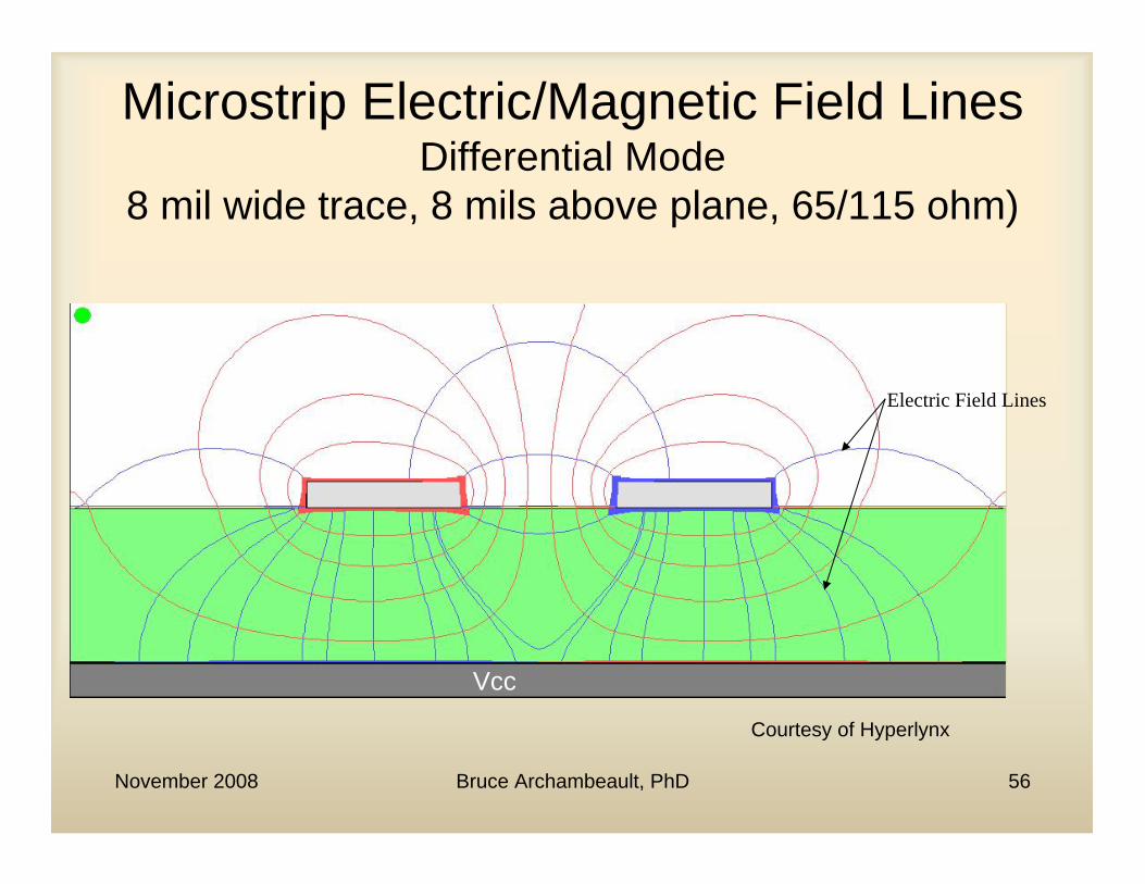
November 2008 Bruce Archambeault, PhD 56
Microstrip Electric/Magnetic Field LinesDifferential Mode
8 mil wide trace, 8 mils above plane, 65/115 ohm)
Electric Field Lines
Vcc
Courtesy of Hyperlynx

November 2008 Bruce Archambeault, PhD 57
Electric/Magnetic Field LinesSymmetrical Stripline
Vcc
GND
Courtesy of Hyperlynx

November 2008 Bruce Archambeault, PhD 58
Electric/Magnetic Field LinesSymmetrical Stripline (Differential)
Vcc
GND
Courtesy of Hyperlynx
November 2008 Bruce Archambeault, PhD 59
Electric/Magnetic Field LinesAsymmetrical Stripline
Vcc
GND
Courtesy of Hyperlynx

November 2008 Bruce Archambeault, PhD 60
Electric/Magnetic Field LinesAsymmetrical Stripline (Differential)
Courtesy of Hyperlynx
November 2008 Bruce Archambeault, PhD 61
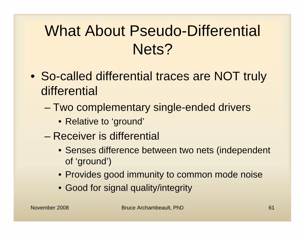
What About Pseudo-Differential Nets?
• So-called differential traces are NOT truly differential– Two complementary single-ended drivers
• Relative to ‘ground’– Receiver is differential
• Senses difference between two nets (independent of ‘ground’)
• Provides good immunity to common mode noise• Good for signal quality/integrity

November 2008 Bruce Archambeault, PhD 62
Pseudo-Differential Nets Current in Nearby Plane
• Balanced/Differential currents have matching current in nearby plane– No issue for discontinuities
• Any unbalanced (common mode) currents have return currents in nearby plane that must return to source!– All normal concerns for single-ended nets
apply!
November 2008 Bruce Archambeault, PhD 63
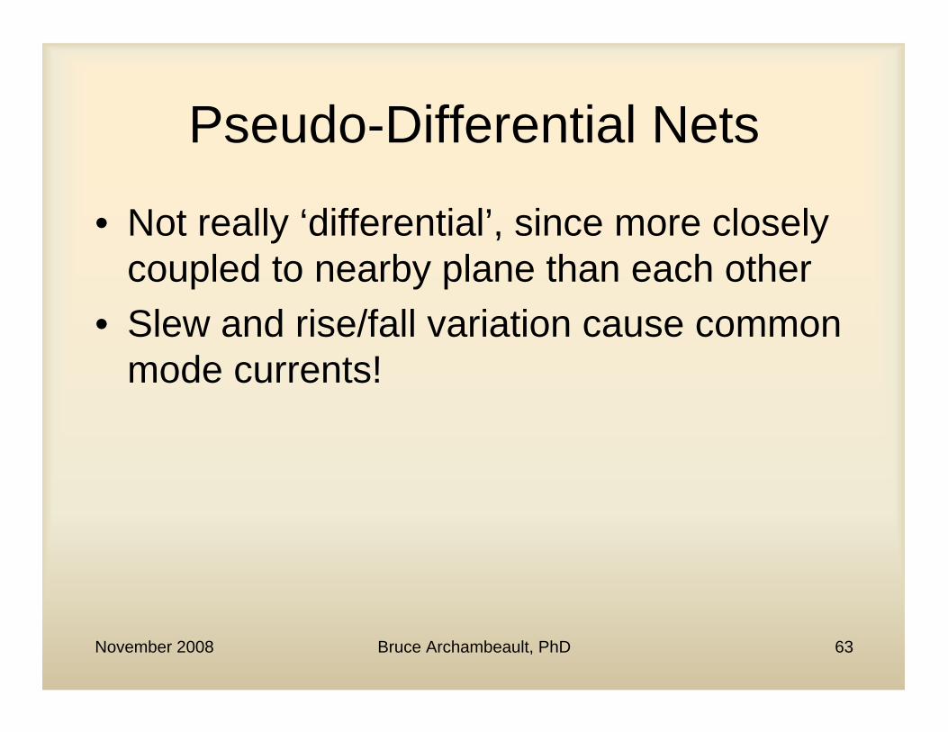
Pseudo-Differential Nets
• Not really ‘differential’, since more closely coupled to nearby plane than each other
• Slew and rise/fall variation cause common mode currents!

November 2008 Bruce Archambeault, PhD 64
Differential Voltage Pulse with Skew1 Gbit/sec with 95 psec rise/fall time
0
0.2
0.4
0.6
0.8
1
1.2
0 0.1 0.2 0.3 0.4 0.5 0.6 0.7 0.8 0.9 1
Time (nsec)
Volta
ge
Complementary -- Line1Complementary -- Line 2Skew=2psSkew=6psSkew = 10psSkew = 20psSkew = 30psSkew =40psSkew =50psSkew =60ps

November 2008 Bruce Archambeault, PhD 65
Common Mode VoltageFrom Differential Voltage Pulse with Skew
1 Gbit/sec with 95 psec rise/fall time
-0.6
-0.4
-0.2
0
0.2
0.4
0.6
0 0.1 0.2 0.3 0.4 0.5 0.6 0.7 0.8 0.9 1
Time (nsec)
Volta
ge
BalancedSkew=2psSkew=6psSkew =10psSkew =20psSkew =30psSkew =40psSkew =50ps

November 2008 Bruce Archambeault, PhD 66
Common Mode CurrentFrom Differential Voltage Pulse with Skew
1 Gbit/sec with 95 psec Rise/fall Time
-100
-80
-60
-40
-20
0
20
40
60
80
100
0 0.1 0.2 0.3 0.4 0.5 0.6 0.7 0.8 0.9 1
Time (nsec)
Leve
l (m
a)
BalancedSkew=2psSkew=6psSkew =10psSkew =20psSkew =30psSkew =40psSkew =50psSkew =60ps

November 2008 Bruce Archambeault, PhD 67
Common Mode CurrentFrom Differential Voltage Pulse with Skew
1 Gbit/sec with 95 psec Rise/fall Time
50
60
70
80
90
100
110
120
130
140
150
1.E+08 1.E+09 1.E+10 1.E+11
Frequency (Hz)
Leve
l (dB
uA)
Skew=2psSkew=6psSkew =10psSkew =20psSkew =30psSkew =40psSkew =50psSkew =60ps

November 2008 Bruce Archambeault, PhD 68
Differential Voltage Pulse with Rise/Fall Variation/Unbalance1 Gbit/sec with 95 psec Nominal Rise/Fall Time
0
0.2
0.4
0.6
0.8
1
1.2
0 0.1 0.2 0.3 0.4 0.5 0.6 0.7 0.8 0.9 1
Time (ns)
Leve
l (vo
lts) Original Pulse rise=95ps
Complementary Pulse Rise=90psComplementary Pulse Rise=80psComplementary Pulse Rise=105psComplementary Pulse Rise=115ps
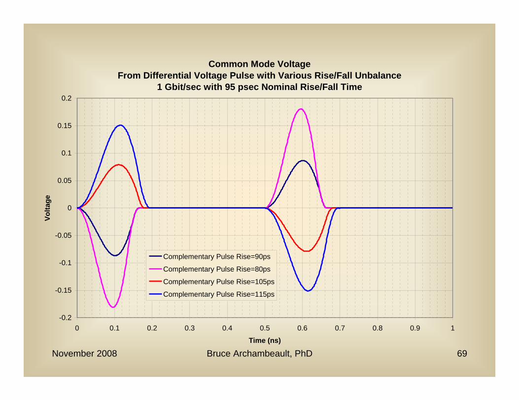
November 2008 Bruce Archambeault, PhD 69
Common Mode VoltageFrom Differential Voltage Pulse with Various Rise/Fall Unbalance
1 Gbit/sec with 95 psec Nominal Rise/Fall Time
-0.2
-0.15
-0.1
-0.05
0
0.05
0.1
0.15
0.2
0 0.1 0.2 0.3 0.4 0.5 0.6 0.7 0.8 0.9 1
Time (ns)
Volta
ge
Complementary Pulse Rise=90ps
Complementary Pulse Rise=80ps
Complementary Pulse Rise=105ps
Complementary Pulse Rise=115ps

November 2008 Bruce Archambeault, PhD 70
Common Mode CurrentFrom Differential Voltage Pulse with Various Rise/Fall Unbalance
1 Gbit/sec with 95 psec Nominal Rise/fall Time
-60
-40
-20
0
20
40
60
0 0.1 0.2 0.3 0.4 0.5 0.6 0.7 0.8 0.9 1
Time (ns)
Cur
rent
(ma)
Complementary Pulse Rise=90psComplementary Pulse Rise=80psComplementary Pulse Rise=105psComplementary Pulse Rise=115ps

November 2008 Bruce Archambeault, PhD 71
Common Mode CurrentFrom Differential Voltage Pulse with Various Rise/Fall Unbalance
1 Gbit/sec with Nominal 95 psec Rise/fall Time
50
55
60
65
70
75
80
85
90
1.E+08 1.E+09 1.E+10 1.E+11
Frequency (Hz)
Leve
l (dB
ua)
Complementary Pulse Rise=90psComplementary Pulse Rise=80psComplementary Pulse Rise=105psComplementary Pulse Rise=115ps

November 2008 Bruce Archambeault, PhD 72
Antenna StructuresDipole antenna
PCB GND planes
Non-Dipole antenna
November 2008 Bruce Archambeault, PhD 73
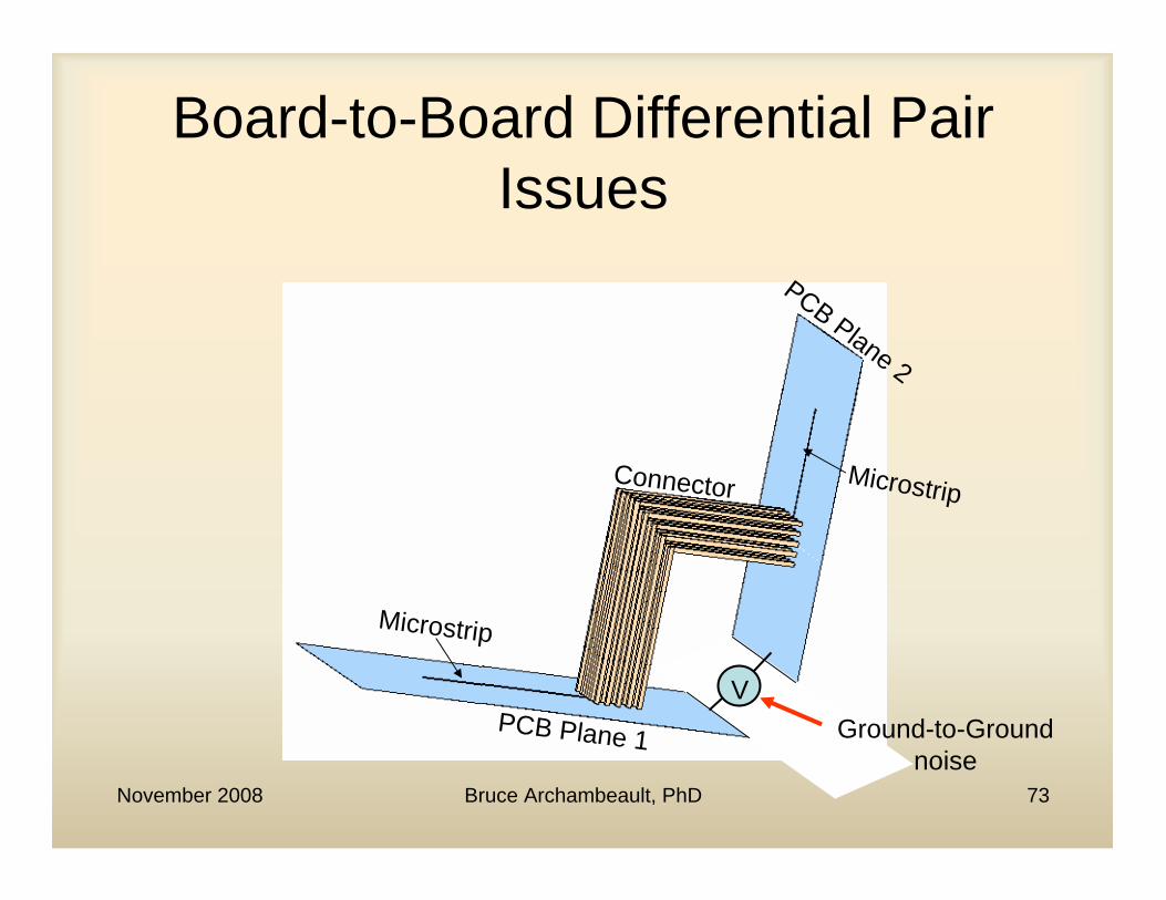
Board-to-Board Differential Pair Issues
Connector
PCB Plane 1
PCB Plane 2
Microstrip
Microstrip
VGround-to-Ground
noise

November 2008 Bruce Archambeault, PhD 74
Example Measured Differential Individual Signal-to-GND
Individual Differential Signals ADDED
Common Mode Noise 170 mV P-P
500 mV P-P (each)

November 2008 Bruce Archambeault, PhD 75
Measured GND-to-GND Voltage
205 mV P-P
November 2008 Bruce Archambeault, PhD 76
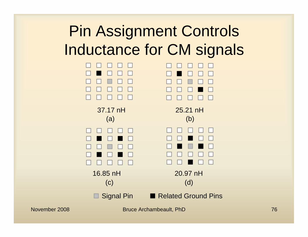
Pin Assignment Controls Inductance for CM signals
Signal Pin Related Ground Pins
37.17 nH 25.21 nH
16.85 nH 20.97 nH
(a) (b)
(c) (d)
November 2008 Bruce Archambeault, PhD 77
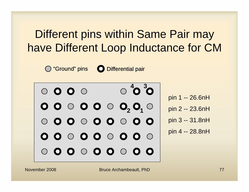
Different pins within Same Pair may have Different Loop Inductance for CM
“Ground” pins Differential pair
2 1
34
“Ground” pins Differential pair
2 1
34
pin 1 -- 26.6nH
pin 2 -- 23.6nH
pin 3 -- 31.8nH
pin 4 -- 28.8nH

November 2008 Bruce Archambeault, PhD 78
Pseudo-Differential Net Summary
• Small amounts of skew can cause significant common mode current
• Small amount of rise/fall time deviation can cause significant amount of common mode current
• Discontinuities (vias, crossing split planes, etc) and convert significant amount of differential current into common mode current

November 2008 Bruce Archambeault, PhD 79
Return Current vs. “Ground”
• For high frequency signals, “Ground” is a concept that does not exist
• The important question is “where does the return current flow?”

November 2008 Bruce Archambeault, PhD 80
Referencing Nets(Where does the Return Current Flow??)
• Microstrip/Stripline across split in reference plane
• Microstrip/Stripline through via (change reference planes)
• Mother/Daughter card

November 2008 Bruce Archambeault, PhD 81
• Don’t Cross Splits with Critical Signals!!!– Bad practice– Stitching capacitor required across split to
allow return current flow• must be close to crossing• must have low inductance• limited frequency effect --- due to inductance
– Major source of Common Mode current!
Microstrip/Stripline Across Split in Reference Plane

November 2008 Bruce Archambeault, PhD 82
Splits in Reference Plane
• Power planes often have splits• Return current path interrupted• Consider spectrum of clock signal• Consider stitching capacitor
impedance• High frequency harmonics not
returned directly

November 2008 Bruce Archambeault, PhD 83
Split Reference Plane Example
PWR
GND
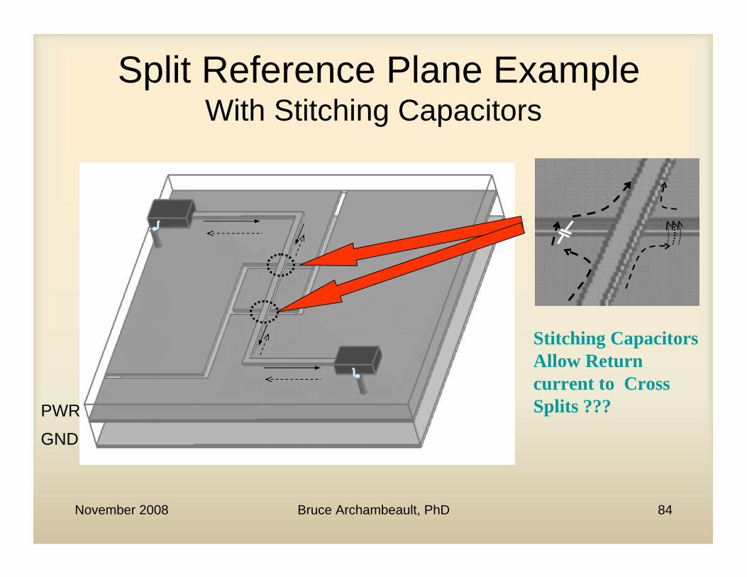
November 2008 Bruce Archambeault, PhD 84
Split Reference Plane Example With Stitching Capacitors
PWR
GND
Stitching Capacitors Allow Return current to Cross Splits ???

November 2008 Bruce Archambeault, PhD 85
Capacitor ImpedanceMeasured Impedance of .01 uf Capacitor
0.1
1.0
10.0
100.0
1.E+06 1.E+07 1.E+08 1.E+09
Frequency (Hz)
Impe
dnac
e (o
hms)
November 2008 Bruce Archambeault, PhD 86
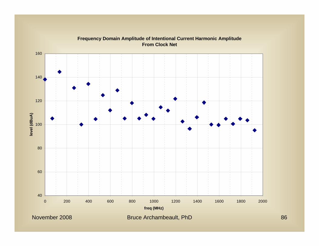
Frequency Domain Amplitude of Intentional Current Harmonic AmplitudeFrom Clock Net
40
60
80
100
120
140
160
0 200 400 600 800 1000 1200 1400 1600 1800 2000
freq (MHz)
leve
l (dB
uA)

November 2008 Bruce Archambeault, PhD 87
MoM Microstrip Model Current Distribution Example

November 2008 Bruce Archambeault, PhD 88
MoM Microstrip Model Current Distribution Example

November 2008 Bruce Archambeault, PhD 89
Emissions From Board
• Far field emissions not important unless it is an unshielded product
• Near field emissions above board AREimportant
• Example of emissions from board with critical net crossing split reference plane

November 2008 Bruce Archambeault, PhD 90
Near Field Radiation from Microstrip on Board with Split in Reference Plane
Comparison of Maximum Radiated E-Field for MicrostripWith and without Split Ground Reference Plane
20
30
40
50
60
70
80
90
100
110
120
10 100 1000
Frequency (MHz)
Max
imum
Rad
iate
d E-
Fiel
d (d
Buv
/m)
No-Split
Split
November 2008 Bruce Archambeault, PhD 91
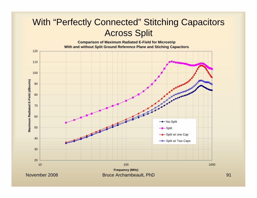
With “Perfectly Connected” Stitching Capacitors Across Split
Comparison of Maximum Radiated E-Field for MicrostripWith and without Split Ground Reference Plane and Stiching Capacitors
20
30
40
50
60
70
80
90
100
110
120
10 100 1000
Frequency (MHz)
Max
imum
Rad
iate
d E-
Fiel
d (d
Buv
/m)
No-Split
Split
Split w/ one Cap
Split w/ Two Caps

November 2008 Bruce Archambeault, PhD 92
Stitching Caps with Via InductanceComparison of Maximum Radiated E-Field for Microstrip
With and without Split Ground Reference Plane and Stiching Capacitors
20
30
40
50
60
70
80
90
100
110
120
10 100 1000
Frequency (MHz)
Max
imum
Rad
iate
d E-
Fiel
d (d
Buv
/m)
No-SplitSplitSplit w/ one CapSplit w/ Two CapsSplit w/One Real CapSplit w/Two Real Caps

November 2008 Bruce Archambeault, PhD 93
Example of Common-Mode Noise Voltage Across Split Plane Vs. Stitching Capacitor Distance to Crossing Point
0
5
10
15
20
25
0 200 400 600 800 1000 1200 1400 1600 1800 2000
Distance (mils)
Gap
Vol
tage
100MHz200MHz300MHz400MHz500MHz600MHz700MHz800MHz900MHz1000MHz

November 2008 Bruce Archambeault, PhD 94
Are Stitching Capacitors Effective ???
• YES, at low frequencies • No, at high frequencies• Need to limit the high frequency current
spectrum• Need to avoid split crossings with ALL
critical signals

November 2008 Bruce Archambeault, PhD 95
Pin Field Via Keepouts??
Return Current must go around entire keep out area --- just as bad as a slot
Return current path deviation minimal
sd
Recommend s/d > 1/3

November 2008 Bruce Archambeault, PhD 96
Changing Reference Planes Six-Layer PCB Stackup Example
Signal Layer
Signal Layer
Signal Layer
Signal Layer
Plane
Plane

November 2008 Bruce Archambeault, PhD 97
Microstrip/Stripline through via (change reference planes)
TraceVia

November 2008 Bruce Archambeault, PhD 98
How can the Return Current Flow When Signal Line Goes Through Via??
What happens to Return Current in this Region?
Return Current

November 2008 Bruce Archambeault, PhD 99
How can the Return Current Flow When Signal Line Goes Through
Via??• Current can NOT go from one side of the
plane to the other through the plane– skin depth
• Current must go around plane at via hole, through decoupling capacitor, around second plane at the second via hole!
• Use displacement current between planes

November 2008 Bruce Archambeault, PhD 100
Reference Planes
What happens to Return Current in this Region?
Return Current Trace Current
Displacement Current
Return Current Across Reference Plane Change
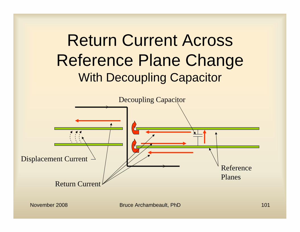
November 2008 Bruce Archambeault, PhD 101
Return Current Across Reference Plane Change
With Decoupling Capacitor
Reference Planes
Return Current
Decoupling Capacitor
Displacement Current

November 2008 Bruce Archambeault, PhD 102
Return Current Across Reference Plane Change With Decoupling Capacitor (on Top)
Return Current
Decoupling Capacitor
Reference Planes
Displacement Current
Common-Mode Current
November 2008 Bruce Archambeault, PhD 103June 2007 103
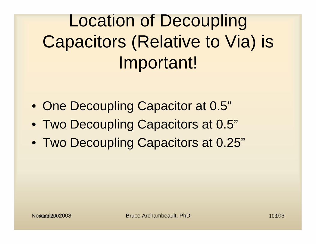
Location of Decoupling Capacitors (Relative to Via) is
Important!
• One Decoupling Capacitor at 0.5”• Two Decoupling Capacitors at 0.5”• Two Decoupling Capacitors at 0.25”

November 2008 Bruce Archambeault, PhD 104June 2007 104
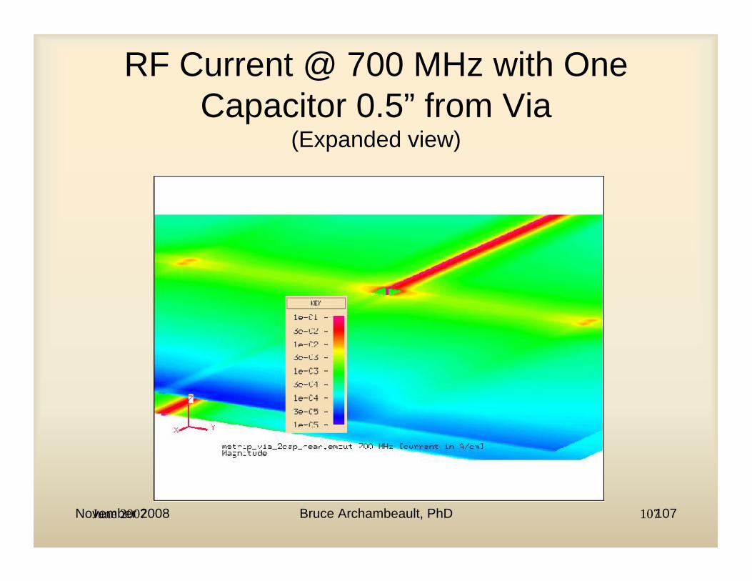
RF Current @ 700 MHz with One Capacitor 0.5” from Via

November 2008 Bruce Archambeault, PhD 105June 2007 105
RF Current @ 700 MHz with One Capacitor 0.5” from Via
(expanded view)

November 2008 Bruce Archambeault, PhD 106June 2007 106
RF Current @ 700 MHz with Two Capacitors 0.5” from Via
November 2008 Bruce Archambeault, PhD 107June 2007 107
RF Current @ 700 MHz with One Capacitor 0.5” from Via
(Expanded view)

November 2008 Bruce Archambeault, PhD 108June 2007 108
RF Current @ 700 MHz with Two Capacitors 0.25” from Via
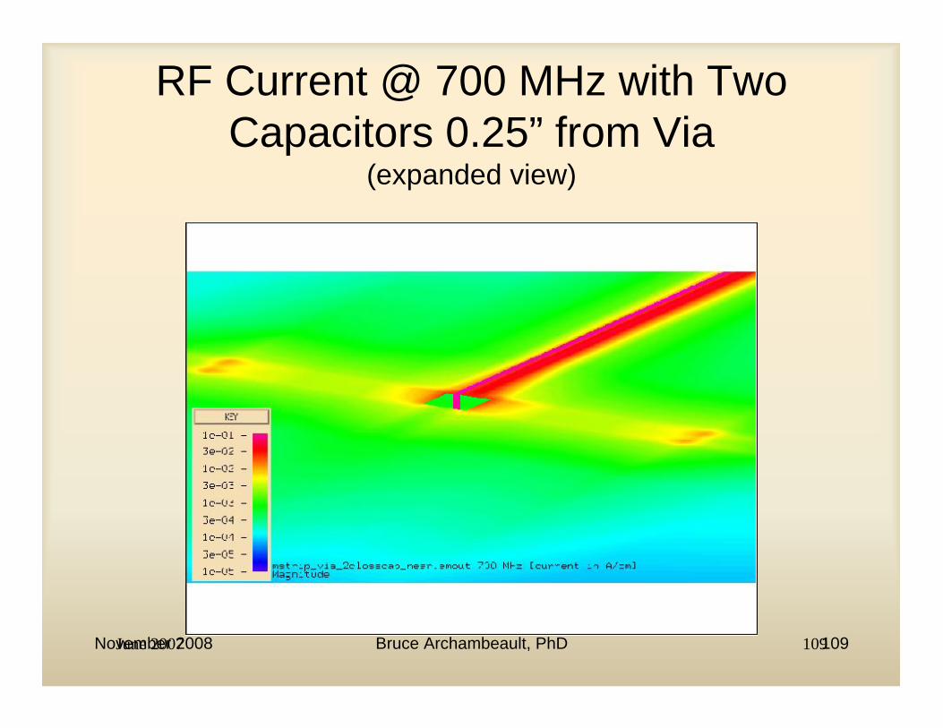
November 2008 Bruce Archambeault, PhD 109June 2007 109
RF Current @ 700 MHz with Two Capacitors 0.25” from Via
(expanded view)

November 2008 Bruce Archambeault, PhD 110June 2007 110
RF Current @ 700 MHz with One REAL Capacitor 0.5” from Via

November 2008 Bruce Archambeault, PhD 111June 2007 111
RF Current @ 700 MHz with Two REAL Capacitors 0.5” from Via

November 2008 Bruce Archambeault, PhD 112June 2007 112
RF Current @ 700 MHz with Two REAL Capacitors 0.25” from Via

November 2008 Bruce Archambeault, PhD 113
BadSignal Layer
Signal Layer
Signal Layer
Signal Layer
Reference Plane
Reference Plane
Bad
Signal Layer
Signal Layer
Signal Layer
Signal Layer
Reference Plane
Reference Plane
GoodSignal Layer
Signal Layer
Signal Layer
Signal Layer
Reference Plane
Reference Plane
Possible Routing OptionsSix-Layer Board
November 2008 Bruce Archambeault, PhD 114
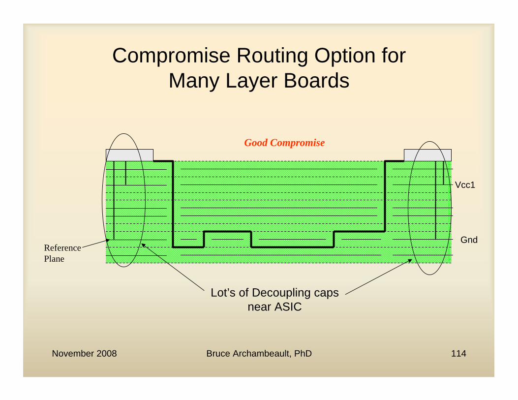
Compromise Routing Option forMany Layer Boards
Good Compromise
Reference Plane
Gnd
Vcc1
Lot’s of Decoupling caps near ASIC
November 2008 Bruce Archambeault, PhD 115
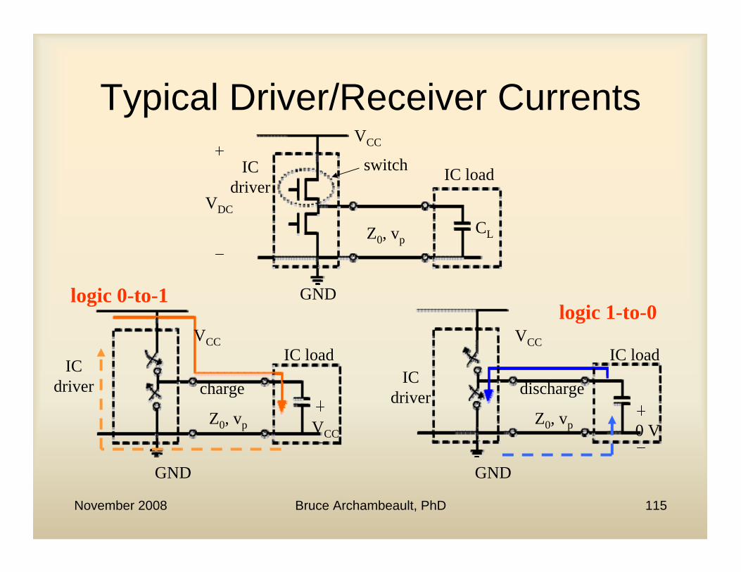
Typical Driver/Receiver Currentsswitch IC loadIC
driverVDC
GND
CL
VCC
Z0, vp
GND
IC loadIC
driver
VCC
VCC
charge
logic 0-to-1
Z0, vp
IC loadIC
driver
GND
VCC
0 V
discharge
logic 1-to-0
Z0, vp
November 2008 Bruce Archambeault, PhD 116
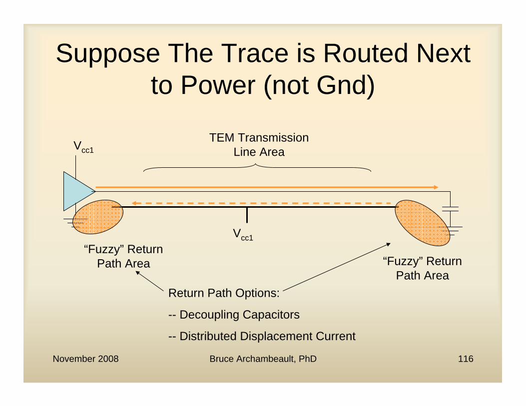
Suppose The Trace is Routed Next to Power (not Gnd)
Vcc1
Vcc1
“Fuzzy” Return Path Area
“Fuzzy” Return Path Area
Return Path Options:
-- Decoupling Capacitors
-- Distributed Displacement Current
TEM Transmission Line Area

November 2008 Bruce Archambeault, PhD 117
Suppose The Trace is Routed Next to a DIFFERENT Power (not Gnd)
Return Path Options:
-- Decoupling Capacitors ??? May not be any nearby!!
-- Distributed Displacement Current – Increased current spread!!!
Vcc1
Vcc2
“Fuzzy” Return Path Area
“Fuzzy” Return Path Area
TEM Transmission Line Area

November 2008 Bruce Archambeault, PhD 118
Via SummaryRoute critical signals on either side of ONE reference planeDrop critical signal net to selected layer close to driver/receiver
Many decoupling capacitors to help return currents
Do NOT change reference planes on critical nets unless ABSOLUTELY NECESSARY!!Make sure at least 2 decoupling capacitors within 0.2” of via with critical signals

November 2008 Bruce Archambeault, PhD 119
Mother/Daughter Board Connector Crossing
• Critical Signals must be referenced to same plane on both sides of the connector

November 2008 Bruce Archambeault, PhD 120
Mother/Daughter Board Connector Crossing
Connector
GND
PWR
Signal Layers
Signal Path

November 2008 Bruce Archambeault, PhD 121
Return Current from Improper Referencing Across Connector
Return current
Connector
Decoupling CapacitorsDisplacement
Current
GND
PWR
Signal Layers
Signal Path

November 2008 Bruce Archambeault, PhD 122
Return Current from Proper Referencing Across Connector
Connector
GND
PWR
Signal Layers
Signal Path
Return current
November 2008 Bruce Archambeault, PhD 123
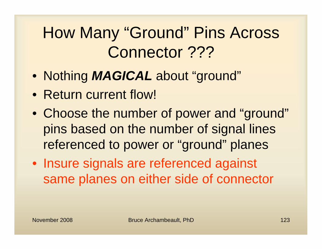
How Many “Ground” Pins Across Connector ???
• Nothing MAGICAL about “ground”• Return current flow!• Choose the number of power and “ground”
pins based on the number of signal lines referenced to power or “ground” planes
• Insure signals are referenced against same planes on either side of connector

November 2008 Bruce Archambeault, PhD 124
Think about Return Currents!!
Reference plane should be continuous under all critical tracesWhen Vias are necessary make sure there are two close decoupling capacitorsWhen crossing a connector to a second board, make sure the critical trace is referenced to the same reference plane as the primary board

November 2008 Bruce Archambeault, PhD 125
Ground-Reference Plane Noise(Voltage Difference Across Plane)
• Connection of large PC ‘ground’ planes to chassis important– ESD current can result in voltage difference
across ‘ground’ plane– Looks like input pulse to circuits– More connection to chassis will reduce this
voltage difference

November 2008 Bruce Archambeault, PhD 126
Connection to Chassis
Good connection in I/O area important for emissions control!!
Connection to chassis away from I/O area NOT important for emissions control
Chassis
PCB gnd plane
Screw post

November 2008 Bruce Archambeault, PhD 127
Connection to Chassis for ESD Control
Distributed Connection to chassis away from I/O area very important for ESD control
Chassis
PCB gnd plane
Screw post

November 2008 Bruce Archambeault, PhD 128
Contacts for Chassis Connection
Screw head contact pad on top of PC Board
Vias to “Ground” planeCopper pad
Screw head
Want this!
NOT this!

November 2008 Bruce Archambeault, PhD 129
Model for Current Simulations
Chassis
PCB gnd planeScrew post
Trace Source
Trace Load
ESD Voltage Between Chassis and gnd plane

November 2008 Bruce Archambeault, PhD 130
Comparison of Trace Load Noise Voltagefor 1 Kv ESD Pulse from PCB GND to Chassis
-1.5
-1
-0.5
0
0.5
1
1.5
2
0 0.5 1 1.5 2 2.5 3 3.5
Time (ns)
Load
Vol
tage
(vol
ts)
No Connection to ChassisOne connection to Chassis (Near I/O)Four Connections to Chassis (Near I/O)Eight Connections to Chassis 16 Connections to Chassis 20 Connections to Chassis

November 2008 Bruce Archambeault, PhD 131
Comparison of Trace Load Noise Voltagefor 1 Kv ESD Pulse from PCB GND to Chassis
-3
-2.5
-2
-1.5
-1
-0.5
0
0.5
1
1.5
2
2.5
0 0.5 1 1.5 2 2.5 3 3.5 4 4.5 5
Time (ns)
Load
Vol
tage
(vol
ts)
No Connection to Chassis
One connection to Chassis (Near I/O)
Four Connections to Chassis (Near I/O)
Eight Connections to Chassis
16 Connections to Chassis
20 Connections to Chassis
Eight Connections to Chassis (4 @each end)

November 2008 Bruce Archambeault, PhD 132
Current Flow w/One Screw Post

November 2008 Bruce Archambeault, PhD 133
Current Flow w/Eight Screw Posts

November 2008 Bruce Archambeault, PhD 134
Current Flow w/20 Screw Posts
November 2008 Bruce Archambeault, PhD 135
Current Flow w/Eight Screw Posts (4 each end)
November 2008 Bruce Archambeault, PhD 136
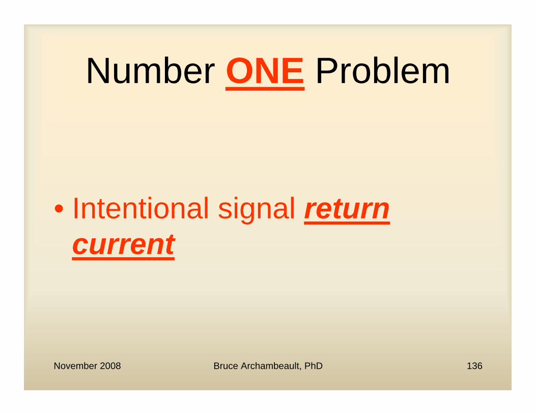
Number ONE Problem
• Intentional signal return current

November 2008 Bruce Archambeault, PhD 137
Where to Go for More?
• Limited selection of EMC design books– Beware of some popular books!!!– “PCB Design for Real-World EMI Control” (good choice)
• Bruce Archambeault
• EMC ‘experts’– Experience is important– Again, beware ---- ask questions and understand WHY
• Cookbooks do not work! Every case is special and different


![[Archambeault B.] PCB Decoupling Capacitor Perform(BookZZ.org)](https://img.pdfslide.net/doc/110x75/5695cefb1a28ab9b028c0e40/archambeault-b-pcb-decoupling-capacitor-performbookzzorg.jpg)


![343o de Vereadores [Modo de Compatibilidade])€¦ · CF/67 AI 07/69 EC 01/69 EC 04/75 + de 100 mil hab. + de 300 mil + de 200 mil hab. 100% Histórico Constitucional e legal da remuneração](https://img.pdfslide.net/doc/110x75/602aabf1fc472622150b4638/343o-de-vereadores-modo-de-compatibilidade-cf67-ai-0769-ec-0169-ec-0475-.jpg)