Embed Size (px)
Citation preview
Humphreys, C. J., Griffiths, J. T., Tang, F., Oehler, F., Findlay, S. D., Zheng,C., ... Oliver, R. A. (2017). The atomic structure of polar and non-polarInGaN quantum wells and the green gap problem. Ultramicroscopy, 176,93–98. DOI: 10.1016/j.ultramic.2017.01.019
Publisher's PDF, also known as Version of record
License (if available):CC BY
Link to published version (if available):10.1016/j.ultramic.2017.01.019
Link to publication record in Explore Bristol ResearchPDF-document
This is the final published version of the article (version of record). It first appeared online via Elsevier athttp://www.sciencedirect.com/science/article/pii/S0304399117300487. Please refer to any applicable terms ofuse of the publisher.
University of Bristol - Explore Bristol ResearchGeneral rights
This document is made available in accordance with publisher policies. Please cite only the publishedversion using the reference above. Full terms of use are available:http://www.bristol.ac.uk/pure/about/ebr-terms
Ultramicroscopy 176 (2017) 93–98
Contents lists available at ScienceDirect
Ultramicroscopy
http://d0304-39
* CorrE-m
jg641@cfabrice.ochanglinjoanne.etomas.mpaul.bagmichaeldanny.sphilip.dsiyuan.zmjk30@
journal homepage: www.elsevier.com/locate/ultramic
The atomic structure of polar and non-polar InGaN quantum wells andthe green gap problem
C.J. Humphreys a,*, J.T. Griffiths a, F. Tang a, F. Oehler b, S.D. Findlay c, C. Zheng d, J. Etheridge e,T.L. Martin f, P.A.J. Bagot f, M.P. Moody f, D. Sutherland g, P. Dawson g, S. Schulz h, S. Zhang a,W.Y. Fu a, T. Zhu a, M.J. Kappers a, R.A. Oliver a
a Department of Materials Science and Metallurgy, University of Cambridge, 27 Charles Babbage Road, Cambridge CB3 0FS, UKb CNRS/C2N, Paris Sud University, Route de Nozay, 91460 Marcoussis, Francec School of Physics and Astronomy, Monash University, Victoria 3800, Australiad Monash Centre for Electron Microscopy, Monash University, Victoria 3800, Australiae Department of Materials Science and Engineering, Monash University, Victoria 3800, Australiaf Department of Materials, University of Oxford, Parks Road, Oxford OX1 3PH, UKg School of Physics and Astronomy, Photon Science Institute, University of Manchester, Manchester M13 9PL, UKh Tyndall National Institute, Lee Maltings Complex, Dyke Parade, Cork, Ireland
a r t i c l e i n f o
Article history:Received 18 August 2016Received in revised form10 January 2017Accepted 22 January 2017Available online 3 February 2017
Keywords:Gallium nitrideAtomic structureQuantum wellsQuantitative STEMAberration-corrected electron microscopy
x.doi.org/10.1016/j.ultramic.2017.01.01991/& 2017 The Authors. Published by Elsevie
esponding author.ail addresses: [email protected] (J.T. Griffiths), [email protected] (F. [email protected] (F. Oehler), [email protected]@monash.edu (C. Zheng),[email protected] (J. Etheridge),[email protected] (T.L. Martin),[email protected] (P.A.J. Bagot),[email protected] (M.P. Moody),[email protected] (D. Sutherland),[email protected] (P. Dawson), [email protected] (S. Zhang), [email protected] (W.Ycam.ac.uk (M.J. Kappers), [email protected] (R
a b s t r a c t
We have used high resolution transmission electron microscopy (HRTEM), aberration-corrected quan-titative scanning transmission electron microscopy (Q-STEM), atom probe tomography (APT) and X-raydiffraction (XRD) to study the atomic structure of (0001) polar and (11-20) non-polar InGaN quantumwells (QWs). This paper provides an overview of the results. Polar (0001) InGaN in QWs is a randomalloy, with In replacing Ga randomly. The InGaN QWs have atomic height interface steps, resulting in QWwidth fluctuations. The electrons are localised at the top QW interface by the built-in electric field andthe well-width fluctuations, with a localisation energy of typically 20meV. The holes are localised nearthe bottom QW interface, by indium fluctuations in the random alloy, with a localisation energy of ty-pically 60meV. On the other hand, the non-polar (11-20) InGaN QWs contain nanometre-scale indium-rich clusters which we suggest localise the carriers and produce longer wavelength (lower energy)emission than from random alloy non-polar InGaN QWs of the same average composition. The reason forthe indium-rich clusters in non-polar (11-20) InGaN QWs is not yet clear, but may be connected to thelower QW growth temperature for the (11-20) InGaN QWs compared to the (0001) polar InGaN QWs.& 2017 The Authors. Published by Elsevier B.V. This is an open access article under the CC BY license
(http://creativecommons.org/licenses/by/4.0/).
1. Introduction
Bob Sinclair and Nestor Zaluzec have pioneered the use ofelectron microscopy and analysis to characterise the structure ofmaterials at the nanoscale. High resolution electron microscopy
r B.V. This is an open access article
k (C.J. Humphreys),ang),onash.edu (S.D. Findlay),
[email protected] (S. Schulz),. Fu),.A. Oliver).
has been central to the research of Sinclair, particularly aberration-corrected transmission electron microscopy. He has utilised highresolution electron microscopy to analyse a wide range of mate-rials and devices, from seminal work on silicide thin-films on si-licon [1] to quantum dots in living mice [2].
Zaluzec has developed state-of-the-art instrumentation forelectron and X-ray spectroscopy, and analytical electron micro-scopy. He has recently investigated how aberration-correctedtransmission electron microscopes can be re-engineered to im-prove the sensitivity of spectroscopy in analytical modes. He hasstudied a wide range of materials, from ground-breaking researchon high-Tc superconductors [3] to InGaN quantum wells in lightemitting diodes [4].
The present paper reports some of our research on the unusualatomic structure of InGaN quantum wells, which relates to thework of Zaluzec [4] and for which aberration-corrected electronmicroscopy has been essential.
under the CC BY license (http://creativecommons.org/licenses/by/4.0/).
C.J. Humphreys et al. / Ultramicroscopy 176 (2017) 93–9894
2. The surprising success of InGaN quantum wells
The use of InGaN light emitting diodes (LEDs) in solid statelighting and high brightness displays is rapidly increasing [5], andit seems likely that InGaN LEDs will become the dominant form oflighting throughout the world, saving over 10% of electricityglobally and 10% of carbon emissions from power stations. At theheart of these LEDs are polar InGaN/GaN quantum wells (QWs)which emit visible light with high internal quantum efficiency(IQE). For example, such blue light emitting LEDs can exhibit IQEvalues as high as 90% at room temperature [6]. This high efficiencyis surprising because the lattice mismatch of GaN on sapphire (theusual substrate in commercial GaN LEDs) is 16%, which leads to ahigh density of misfit dislocations at the GaN/sapphire interfaceand to threading dislocations passing through the InGaN QWswith a density of at least 108cm�2. In other light-emitting semi-conductors, such as GaAs, the dislocation density needs to be lessthan 103cm�2 to prevent significant loss of light due to the non-radiative recombination of carriers at the dislocations. It is knownfrom cathodoluminescence (CL) studies that dislocations in InGaNare non-radiative recombination centres. Hence a key question iswhy the efficiency of blue emitting InGaN/GaN LEDs is so highwhen the dislocation density is so large.
3. The green gap problem in LEDs
White LEDs used for lighting typically use a blue-emitting In-GaN/GaN LED covered with a yellow emitting phosphor, thecombination of blue and yellow light producing a cool white light.If a warmer white light is desired, a red emitting phosphor is usedas well. However, the obvious way to produce white light is to mixred, green and blue LEDs. This would produce even more efficientwhite light than using a blue LED with phosphors because theStokes shift energy loss of converting a high energy blue photon toa lower energy yellow or red photon would be avoided, as wouldefficiency losses in the phosphors themselves. However, we cannotdo this efficiently at present due to the “green gap” problem. Theexperimentally determined external quantum efficiency (EQE) of400nm (violet) LEDs is very high, over 80%, and for 650nm (red), itis also very high, over 70%, but for green and yellow emission theEQE drops to about 20% [7]. This “Green Gap” has importanttechnological consequences. If one wishes to make white light bymixing red, green and blue LEDs, one red, one blue and threegreen LEDs are typically required, making such a white lightsource expensive.
The green gap in nitride LEDs may in part be attributed to in-ternal electric fields due to the large spontaneous and piezo-electric polarisations that produce high fields of ∼ 106Vcm�1
across the QWs. The active region in nitride LEDs is one or moreInGaN QWs sandwiched between the wider bandgap GaN barriersto confine the carriers. The epitaxial InGaN QWs are strained be-cause InGaN has a larger lattice parameter than GaN. CommercialInGaN/GaN QW LEDs are grown in the polar [0001] direction. Thestrain in an InGaN QW increases as the indium content increases,hence the piezoelectric field across an InGaN QW increases as theindium content increases. This field separates the electrons andholes to opposite sides of the QW, the separation increasing as theindium content increases. Hence the electron-hole wave-functionoverlap decreases as the indium content increases. This may resultin the efficiency of InGaN/GaN green LEDs being less than that ofblue LEDs because the decreased electron and hole overlap ingreen QWs results in increased radiative lifetimes, which in thepresence of non-radiative recombination paths can lead to re-duced values of the IQE and EQE. The electric field across an InGaNQW can be suppressed by growing the InGaN/GaN QW structure
along a non-polar direction. This would be expected to producegreen LEDs with high efficiency, hence we have recently exploredthis and obtained some surprising results.
4. The atomic structure of polar
It was realised as long ago as 1997 that since blue InGaN QWsemitted brilliant light despite having a very high density of dis-locations, and since cathodoluminescence showed that disloca-tions were non-radiative recombination centres in InGaN, theremust be some microstructural feature of the InGaN QWs that waslocalising the carriers and preventing them from moving to thedislocations. There was at the time broad agreement in the GaNscientific community that indium-rich clusters in the InGaN QWswere responsible for localising the carriers [8-16]. Since thebandgap of InN is smaller than that of GaN, indium-rich clusters inan InGaN QW will have a smaller bandgap and hence localise thecarriers. The widespread belief in this localisation mechanism wasbased upon three pieces of scientific evidence. First, high resolu-tion transmission electron microscopy (HRTEM) revealed localisedregions of strain contrast about 2nm across which were inter-preted as being highly indium rich. This was supported by datafrom electron energy loss spectroscopy (EELS) [8-16]. Second,photoluminescence (PL) measurements of the temperature de-pendence of the peak photon energy emitted from an InGaN QWrevealed an S-shaped dependence characteristic of carrier locali-sation [17]. Thirdly, thermodynamic calculations revealed thatInGaN was an unstable alloy which would decompose into indiumrich and indium poor regions [18]. These three independent piecesof evidence appeared to provide strong scientific support for therebeing gross indium-rich clusters in InGaN QWs, and this wasuniversally accepted by the scientific community.
In 2003, it was shown that InGaN QWs were extremely sensi-tive to radiation damage in TEM and that HRTEM images acquiredimmediately after first irradiating a region of an InGaN QWshowed no detectable indium-rich regions [19-21]. The papersfurther revealed that continued exposure to the electron beam ledto the formation of locally strained regions that appeared similarto those previously attributed to indium rich clusters. So it wasconcluded that the indium-rich clusters observed by many otherswere due to electron beam damage. This was subsequently sup-ported by multiple research groups by a variety of methods [22-27].
However, InGaN can decompose if there are macrosteps on thegrowth surface, since indium is incorporated differently at treadsand risers of these macrosteps, which leads to compositionalgrowth striations [28]. A recent example of this is atomic-levelordering in InGaN quantum dots in GaN nanowires. This was at-tributed to a non-flat growth front at vicinal surface facets [29]. Inother recent work, indium fluctuations were observed in InGaN/GaN core-shell nanorods, and these were correlated with atomicsteps at the GaN/InGaN core-shell interface giving rise to a changein the growth mode from 2D (planar) to 3D (faceted) [30]. Apartfrom these examples of faceted growth, there is now almost uni-versal acceptance that in (0001) InGaN quantum wells grown by2D layer-by-layer growth, as in planar LEDs, there are no grossindium-rich clusters.
Galtrey et al [31] used atom probe tomography (APT) not onlyto confirm that there were no indium-rich clusters in (0001) In-GaN QWs but also to demonstrate that InGaN was a random alloy.APT was also used to show that an electron beam in TEM cancreate In-rich clusters in InGaN [32]. These results appeared toconflict with the thermodynamic calculations that showed thatInGaN should decompose into indium rich and indium poor re-gions at the growth temperature used [18]. However, these
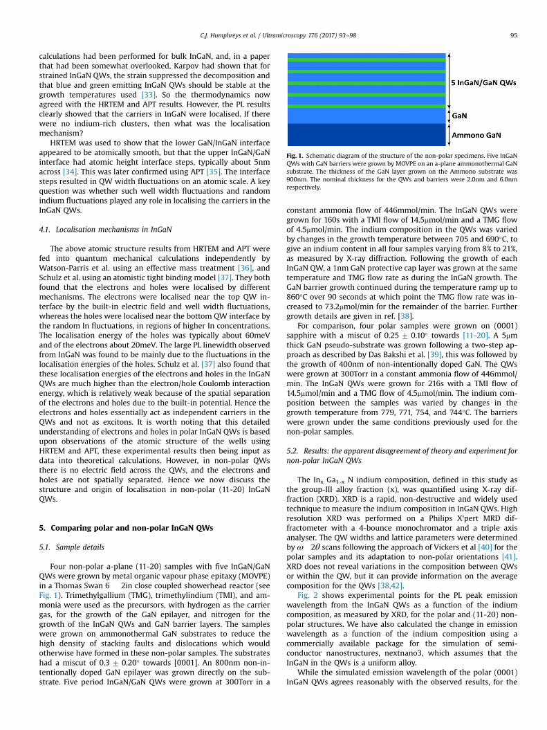
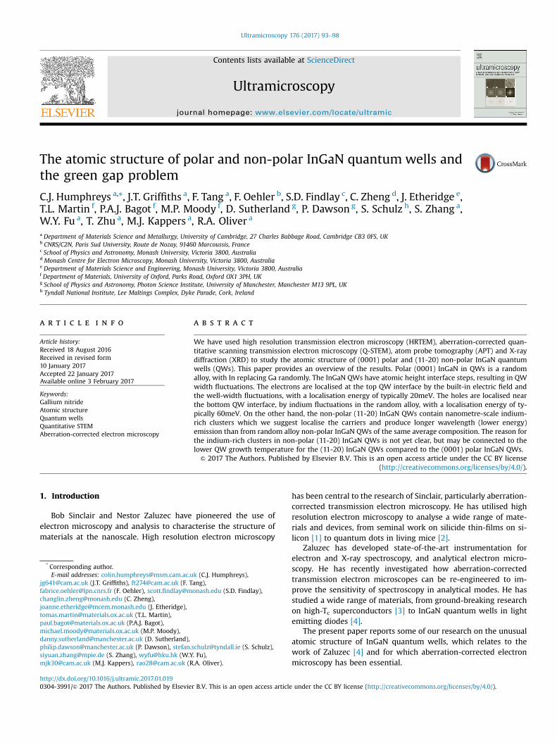
Fig. 1. Schematic diagram of the structure of the non-polar specimens. Five InGaNQWs with GaN barriers were grown by MOVPE on an a-plane ammonothermal GaNsubstrate. The thickness of the GaN layer grown on the Ammono substrate was900nm. The nominal thickness for the QWs and barriers were 2.0nm and 6.0nmrespectively.
C.J. Humphreys et al. / Ultramicroscopy 176 (2017) 93–98 95
calculations had been performed for bulk InGaN, and, in a paperthat had been somewhat overlooked, Karpov had shown that forstrained InGaN QWs, the strain suppressed the decomposition andthat blue and green emitting InGaN QWs should be stable at thegrowth temperatures used [33]. So the thermodynamics nowagreed with the HRTEM and APT results. However, the PL resultsclearly showed that the carriers in InGaN were localised. If therewere no indium-rich clusters, then what was the localisationmechanism?
HRTEM was used to show that the lower GaN/InGaN interfaceappeared to be atomically smooth, but that the upper InGaN/GaNinterface had atomic height interface steps, typically about 5nmacross [34]. This was later confirmed using APT [35]. The interfacesteps resulted in QW width fluctuations on an atomic scale. A keyquestion was whether such well width fluctuations and randomindium fluctuations played any role in localising the carriers in theInGaN QWs.
4.1. Localisation mechanisms in InGaN
The above atomic structure results from HRTEM and APT werefed into quantum mechanical calculations independently byWatson-Parris et al. using an effective mass treatment [36], andSchulz et al. using an atomistic tight binding model [37]. They bothfound that the electrons and holes were localised by differentmechanisms. The electrons were localised near the top QW in-terface by the built-in electric field and well width fluctuations,whereas the holes were localised near the bottom QW interface bythe random In fluctuations, in regions of higher In concentrations.The localisation energy of the holes was typically about 60meVand of the electrons about 20meV. The large PL linewidth observedfrom InGaN was found to be mainly due to the fluctuations in thelocalisation energies of the holes. Schulz et al. [37] also found thatthese localisation energies of the electrons and holes in the InGaNQWs are much higher than the electron/hole Coulomb interactionenergy, which is relatively weak because of the spatial separationof the electrons and holes due to the built-in potential. Hence theelectrons and holes essentially act as independent carriers in theQWs and not as excitons. It is worth noting that this detailedunderstanding of electrons and holes in polar InGaN QWs is basedupon observations of the atomic structure of the wells usingHRTEM and APT, these experimental results then being input asdata into theoretical calculations. However, in non-polar QWsthere is no electric field across the QWs, and the electrons andholes are not spatially separated. Hence we now discuss thestructure and origin of localisation in non-polar (11-20) InGaNQWs.
5. Comparing polar and non-polar InGaN QWs
5.1. Sample details
Four non-polar a-plane (11-20) samples with five InGaN/GaNQWs were grown by metal organic vapour phase epitaxy (MOVPE)in a Thomas Swan 6 � 2in close coupled showerhead reactor (seeFig. 1). Trimethylgallium (TMG), trimethylindium (TMI), and am-monia were used as the precursors, with hydrogen as the carriergas, for the growth of the GaN epilayer, and nitrogen for thegrowth of the InGaN QWs and GaN barrier layers. The sampleswere grown on ammonothermal GaN substrates to reduce thehigh density of stacking faults and dislocations which wouldotherwise have formed in these non-polar samples. The substrateshad a miscut of 0.3 7 0.20° towards [0001]. An 800nm non-in-tentionally doped GaN epilayer was grown directly on the sub-strate. Five period InGaN/GaN QWs were grown at 300Torr in a
constant ammonia flow of 446mmol/min. The InGaN QWs weregrown for 160s with a TMI flow of 14.5mmol/min and a TMG flowof 4.5mmol/min. The indium composition in the QWs was variedby changes in the growth temperature between 705 and 690°C, togive an indium content in all four samples varying from 8% to 21%,as measured by X-ray diffraction. Following the growth of eachInGaN QW, a 1nm GaN protective cap layer was grown at the sametemperature and TMG flow rate as during the InGaN growth. TheGaN barrier growth continued during the temperature ramp up to860°C over 90 seconds at which point the TMG flow rate was in-creased to 73.2mmol/min for the remainder of the barrier. Furthergrowth details are given in ref. [38].
For comparison, four polar samples were grown on (0001)sapphire with a miscut of 0.25 7 0.10° towards [11-20]. A 5mmthick GaN pseudo-substrate was grown following a two-step ap-proach as described by Das Bakshi et al. [39], this was followed bythe growth of 400nm of non-intentionally doped GaN. The QWswere grown at 300Torr in a constant ammonia flow of 446mmol/min. The InGaN QWs were grown for 216s with a TMI flow of14.5mmol/min and a TMG flow of 4.5mmol/min. The indium com-position between the samples was varied by changes in thegrowth temperature from 779, 771, 754, and 744°C. The barrierswere grown under the same conditions previously used for thenon-polar samples.
5.2. Results: the apparent disagreement of theory and experiment fornon-polar InGaN QWs
The Inx Ga1-x N indium composition, defined in this study asthe group-III alloy fraction (x), was quantified using X-ray dif-fraction (XRD). XRD is a rapid, non-destructive and widely usedtechnique to measure the indium composition in InGaN QWs. Highresolution XRD was performed on a Philips X'pert MRD dif-fractometer with a 4-bounce monochromator and a triple axisanalyser. The QW widths and lattice parameters were determinedby ω�2θ scans following the approach of Vickers et al [40] for thepolar samples and its adaptation to non-polar orientations [41].XRD does not reveal variations in the composition between QWsor within the QW, but it can provide information on the averagecomposition for the QWs [38,42].
Fig. 2 shows experimental points for the PL peak emissionwavelength from the InGaN QWs as a function of the indiumcomposition, as measured by XRD, for the polar and (11-20) non-polar structures. We have also calculated the change in emissionwavelength as a function of the indium composition using acommercially available package for the simulation of semi-conductor nanostructures, nextnano3, which assumes that theInGaN in the QWs is a uniform alloy.
While the simulated emission wavelength of the polar (0001)InGaN QWs agrees reasonably with the observed results, for the
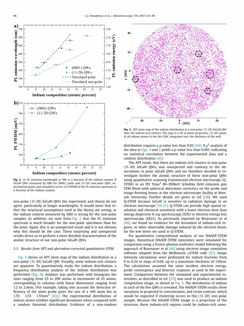
Fig. 2. (a) PL emission wavelength at 10K as a function of the indium content ofInGaN QWs measured by XRD for (0001) polar and (11-20) non-polar QWs, ex-perimental points and simulated curves. (b) FWHM of the PL emission spectrum asa function of the indium content.
Fig. 3. APT atom map of the indium distribution in a non-polar (11-20) InGaN QW.Note the indium-rich clusters. The map is a 2D in-plane projection, (11-20) plane,of all indium atoms in the first QW, integrated over the thickness of the well.
C.J. Humphreys et al. / Ultramicroscopy 176 (2017) 93–9896
non-polar (11-20) InGaN QWs the experiment and theory do notagree, particularly at longer wavelengths. It would seem that ei-ther the structural assumptions used in the theory are wrong, orthe indium content measured by XRD is wrong for the non-polarsamples. In addition, we note from Fig. 2 that the PL emissionspectrum is much broader for the non-polar specimens than forthe polar. Again, this is an unexpected result and it is not obviouswhy this should be the case. These surprising and unexpectedresults drove us to perform a more detailed characterisation of theatomic structure of our non-polar InGaN QWs.
5.3. Results from APT and aberration-corrected quantitative-STEM
Fig. 3 shows an APT atom map of the indium distribution in anon-polar (11-20) InGaN QW. Visually, some indium-rich clustersare apparent. To quantitatively study the indium distribution, afrequency distribution analysis of the indium distribution wasperformed (Fig. 4). Analysis was performed with histogram binsizes ranging from 25 to 200 atoms in increments of 25 atoms,corresponding to volumes with linear dimensions ranging from1.2 to 2.4nm. (For example, taking into account the detection ef-ficiency of the atom probe gives the size of a 100 atom bin as1.55 � 1.55 � 1.55nm3 [43].) The experimental distribution ofindium atoms exhibits significant deviations when compared witha random binomial distribution. Evidence of a non-random
distribution requires a p-value less than 0.05 [44]. A χ2 analysis ofthe data in Figs. 4 and 5 yields a p-value less than 0.001, indicatingno statistical correlation between the experimental data and arandom distribution [45].
The APT result, that there are indium-rich clusters in non-polar(11-20) InGaN QWs, was unexpected and contrary to the ob-servations in polar InGaN QWs and we therefore decided to in-vestigate further the atomic structure of these non-polar QWsusing quantitative scanning transmission electron microscopy (Q-STEM) in an FEI Titan3 80–300keV Schottky field emission gunTEM fitted with spherical aberration correctors on the probe andimage-forming lenses at the electron microscope facility at Mon-ash University. Further details are given in ref. [38]. We usedQ-STEM because InGaN is sensitive to radiation damage in anelectron microscope [19-21]. Q-STEM can provide high spatial re-solution and chemical sensitivity with a lower electron dose thanenergy dispersive X-ray spectroscopy (EDS) or electron energy lossspectroscopy (EELS). As previously reported by Rosenauer et al[46], we found no evidence for the formation of indium-rich re-gions, or other observable damage induced by the electron beam,for the low doses we used in Q-STEM.
For quantitative compositional analysis of our HAADF-STEMimages, theoretical HAADF-STEM intensities were simulated forcomparison using a frozen phonon multislice model following theapproach of Rosenauer et al [46] using electron image simulationsoftware adapted from the Melbourne mSTEM code [47]. Imageintensity calculations were performed for indium fractions from0 to 0.24 in steps of 0.04, up to a maximum thickness of 130nm.The calculations assumed the same incident electron energy,probe convergence and detector response as used in the experi-ment. Comparison between the simulated and experimental in-tensities, as described in ref. [37], was used to produce an indiumcomposition image, as shown in Fig. 5. The distribution of indiumin each of the five QWs is revealed. The HAADF-STEM results showvariations in projected In concentration, and strain contrast, whichwould be expected if clustering occurs in this (11-20) non-polarsample. Because the HAADF-STEM image is a projection of thestructure, these indium-rich regions could be indium-rich nano-
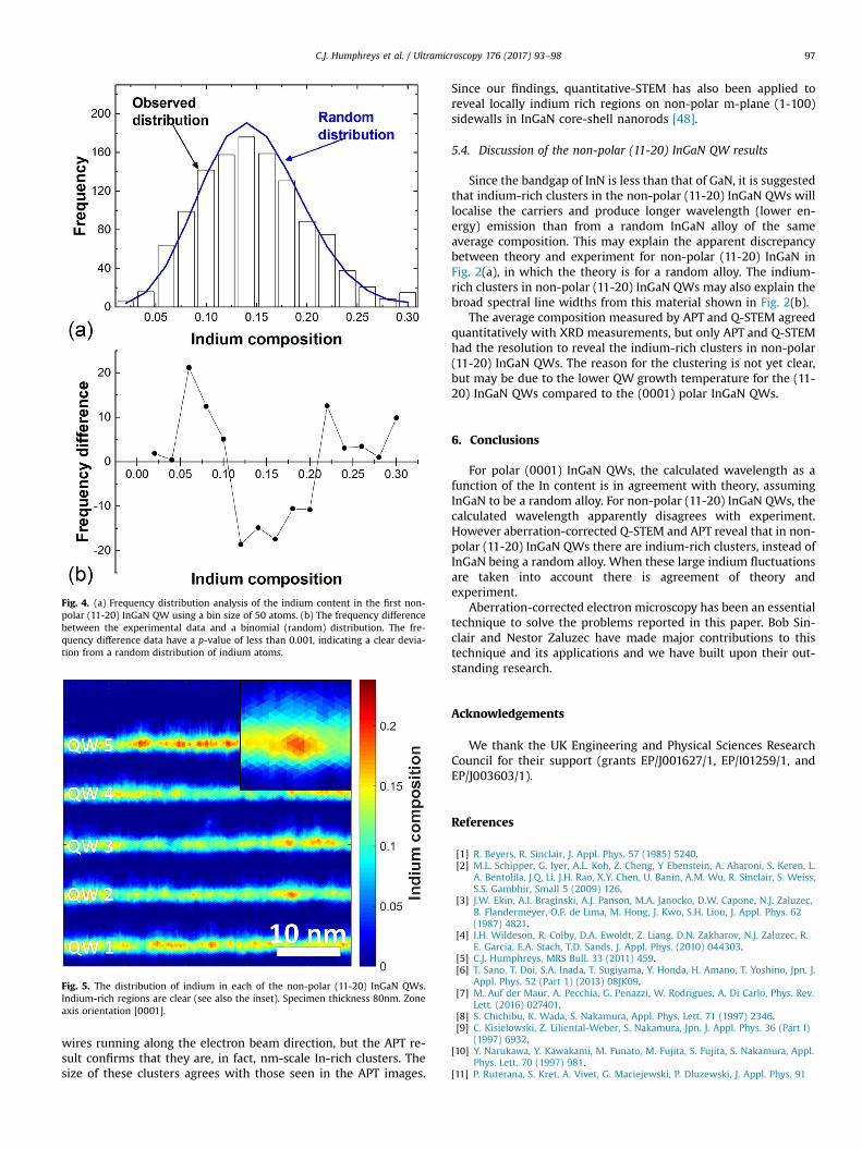
Fig. 5. The distribution of indium in each of the non-polar (11-20) InGaN QWs.Indium-rich regions are clear (see also the inset). Specimen thickness 80nm. Zoneaxis orientation [0001].
Fig. 4. (a) Frequency distribution analysis of the indium content in the first non-polar (11-20) InGaN QW using a bin size of 50 atoms. (b) The frequency differencebetween the experimental data and a binomial (random) distribution. The fre-quency difference data have a p-value of less than 0.001, indicating a clear devia-tion from a random distribution of indium atoms.
C.J. Humphreys et al. / Ultramicroscopy 176 (2017) 93–98 97
wires running along the electron beam direction, but the APT re-sult confirms that they are, in fact, nm-scale In-rich clusters. Thesize of these clusters agrees with those seen in the APT images.
Since our findings, quantitative-STEM has also been applied toreveal locally indium rich regions on non-polar m-plane (1-100)sidewalls in InGaN core-shell nanorods [48].
5.4. Discussion of the non-polar (11-20) InGaN QW results
Since the bandgap of InN is less than that of GaN, it is suggestedthat indium-rich clusters in the non-polar (11-20) InGaN QWs willlocalise the carriers and produce longer wavelength (lower en-ergy) emission than from a random InGaN alloy of the sameaverage composition. This may explain the apparent discrepancybetween theory and experiment for non-polar (11-20) InGaN inFig. 2(a), in which the theory is for a random alloy. The indium-rich clusters in non-polar (11-20) InGaN QWs may also explain thebroad spectral line widths from this material shown in Fig. 2(b).
The average composition measured by APT and Q-STEM agreedquantitatively with XRD measurements, but only APT and Q-STEMhad the resolution to reveal the indium-rich clusters in non-polar(11-20) InGaN QWs. The reason for the clustering is not yet clear,but may be due to the lower QW growth temperature for the (11-20) InGaN QWs compared to the (0001) polar InGaN QWs.
6. Conclusions
For polar (0001) InGaN QWs, the calculated wavelength as afunction of the In content is in agreement with theory, assumingInGaN to be a random alloy. For non-polar (11-20) InGaN QWs, thecalculated wavelength apparently disagrees with experiment.However aberration-corrected Q-STEM and APT reveal that in non-polar (11-20) InGaN QWs there are indium-rich clusters, instead ofInGaN being a random alloy. When these large indium fluctuationsare taken into account there is agreement of theory andexperiment.
Aberration-corrected electron microscopy has been an essentialtechnique to solve the problems reported in this paper. Bob Sin-clair and Nestor Zaluzec have made major contributions to thistechnique and its applications and we have built upon their out-standing research.
Acknowledgements
We thank the UK Engineering and Physical Sciences ResearchCouncil for their support (grants EP/J001627/1, EP/I01259/1, andEP/J003603/1).
References
[1] R. Beyers, R. Sinclair, J. Appl. Phys. 57 (1985) 5240.[2] M.L. Schipper, G. Iyer, A.L. Koh, Z. Cheng, Y Ebenstein, A. Aharoni, S. Keren, L.
A. Bentolila, J.Q. Li, J.H. Rao, X.Y. Chen, U. Banin, A.M. Wu, R. Sinclair, S. Weiss,S.S. Gambhir, Small 5 (2009) 126.
[3] J.W. Ekin, A.I. Braginski, A.J. Panson, M.A. Janocko, D.W. Capone, N.J. Zaluzec,B. Flandermeyer, O.F. de Lima, M. Hong, J. Kwo, S.H. Liou, J. Appl. Phys. 62(1987) 4821.
[4] I.H. Wildeson, R. Colby, D.A. Ewoldt, Z. Liang, D.N. Zakharov, N.J. Zaluzec, R.E. Garcia, E.A. Stach, T.D. Sands, J. Appl. Phys. (2010) 044303.
[5] C.J. Humphreys, MRS Bull. 33 (2011) 459.[6] T. Sano, T. Doi, S.A. Inada, T. Sugiyama, Y. Honda, H. Amano, T. Yoshino, Jpn. J.
Appl. Phys. 52 (Part 1) (2013) 08JK09.[7] M. Auf der Maur, A. Pecchia, G. Penazzi, W. Rodrigues, A. Di Carlo, Phys. Rev.
Lett. (2016) 027401.[8] S. Chichibu, K. Wada, S. Nakamura, Appl. Phys. Lett. 71 (1997) 2346.[9] C. Kisielowski, Z. Liliental-Weber, S. Nakamura, Jpn. J. Appl. Phys. 36 (Part I)
(1997) 6932.[10] Y. Narukawa, Y. Kawakami, M. Funato, M. Fujita, S. Fujita, S. Nakamura, Appl.
Phys. Lett. 70 (1997) 981.[11] P. Ruterana, S. Kret, A. Vivet, G. Maciejewski, P. Dluzewski, J. Appl. Phys. 91

C.J. Humphreys et al. / Ultramicroscopy 176 (2017) 93–9898
(2015) 8979.[12] S. Srinivasan, F. Bertram, A. Bell, F.A. Ponce, S. Tanaka, H. Omiya, Y. Nakagawa,
Appl. Phys. Lett. 80 (2002) 550.[13] F.A. Ponce, S. Srinivasen, A. Bell, L. Geng, R. Liu, M. Stevens, J. Cai, H. Omiya,
H. Marui, S. Tanaka, Phys. Status Solidi B 240 (2003) 273.[14] H.K. Cho, J.Y. Lee1, N. Sharma, C.J. Humphreys, G.M. Yang, C.S. Kim, J.H. Song, P.
W. Yu, Appl. Phys. Lett. 79 (2001) 2594.[15] D. Gerthsen, E. Hahn, B. Neubauer, A. Rosenauer, O. Schön, M. Heuken, A. Rizzi,
Phys. Status Solidi A 177 (2000) 145.[16] H. Lakner, G. Brockt, C. Mendorf, A. Radefeld, F. Scholz, V. Härle, J. Off,
A. Sohmer, J. Electron. Mater. 26 (1997) 1103.[17] Y.H. Cho, G.H. Gainer, A.J. Fischer, J.J. Song, S. Keller, U.K. Mishra, S.P. DenBaars,
Appl. Phys. Lett. 73 (1998) 1370.[18] I. Ho, G.B. Stringfellow, Appl. Phys. Lett. 69 (1996) 2701.[19] T.M. Smeeton, M.J. Kappers, J.S. Barnard, M.E. Vickers, C.J. Humphreys, Phys.
Status Solidi B 204 (2003) 297.[20] J.P. O'Neill, I.M. Ross, A.G. Cullis, T. Wang, P.J. Parbrook, Appl. Phys. Lett. 83
(2003) 1965.[21] T.M. Smeeton, M.J. Kappers, J.S. Barnard, M.E. Vickers, C.J. Humphreys, Appl.
Phys. Lett. 83 (2003) 5419.[22] T. Schulz, T. Remmele, T. Markurt, M. Korytov, M. Albrecht, J. Appl. Phys. (2012)
033106.[23] T. Schulz, A. Duff, T. Remmele, M. Korytov, T. Markurt, M. Albrecht,
L. Lymperakis, J. Neugebauer, C. Chèze, C. Skierbiszewski, J. Appl. Phys. (2014)033113.
[24] X.J. Chen, J.S. Hwang, G. Perillat-Merceroz, S. Landis, B. Martin, D. Le Si Dang,J. Eymery, C. Durand, J. Cryst. Growth 322 (2011) 15.
[25] D. Salomon, A. Dussaigne, M. Lafossas, C. Durand, C. Bougerol, P. Ferret,J. Eymery, Nanoscale Res. Lett. 8 (2013) 61.
[26] L. Rigutti, I. Blum, D. Shinde, D. Herna ́ndez-Maldonado, W. Lefebvre, J. Houard,F. Vurpillot, A. Vella, M. Tchernycheva, C. Durand, J. Eymery, B. Deconihout,Nano Lett. 14 (2014) 107.
[27] T. Walther, H. Amari, I.M. Ross, T. Wang, A.G. Cullis, J. Mater. Science 48 (2013)2883.
[28] M. Kryśko, G. Franssen, T. Suski, M. Albrecht, B. Łucznik, I. Grzegory,S. Krukowski, R. Czernecki, S. Grzanka, I. Makarowa, M. Leszczyński, P. Perlin,Appl. Phys. Lett. (2007) 211904.
[29] S.Y. Woo, M. Bugnet, H.P.T. Nguyen, Z. Mi, G.A. Botton, Nano Lett. 15 (2015)6413.
[30] P.-M. Coulon, S. Hosseini Vajargah, A. Bao, P.R. Edwards, E.D. Le Boulbar,
I. Gîrgel, R.W. Martin, C.J. Humphreys, R.A. Oliver, D.W.E. Allsopp, P.A. Shields,Cryst. Growth Des. 17 (2017) 474.
[31] M.J. Galtrey, R.A. Oliver, M.J. Kappers, C.J. Humphreys, P. Clifton, D. Lawson,D. Saxey, A. Cerezo, J. Appl. Phys. (2008) 013524.
[32] S.E. Bennett, D.W. Saxey, M.J. Kappers, J.S. Barnard, C.J. Humphreys, G.D.W. Smith, R.A. Oliver, Appl. Phys. Lett. (2011) 021906.
[33] S.Y. Karpov, MRS Internet J. Nitride Semicond. Res. 3 (1998) 16.[34] D.M. Graham, A. Soltani-Vala, P. Dawson, M.J. Godfrey, T.M. Smeeton, J.
S. Barnard, M.J. Kappers, C.J. Humphreys, E.J. Thrush, J. Appl. Phys. (2005)103508.
[35] M.J. Galtrey, R.A. Oliver, M.J. Kappers, C.J. Humphreys, P. Clifton, D. Lawson,D. Saxey, A. Cerezo, J. Appl. Phys. (2008) 013524.
[36] D. Watson-Parris, M.J. Godfrey, P. Dawson, R.A. Oliver, M.J. Galtrey, M.J. Kappers, C.J. Humphreys, Phys. Rev. B (2011) 115321.
[37] S. Schulz, M.A. Caro, C. Coughlan, E.P. O'Reilly, Phys. Rev. B (2015) 035439.[38] J.T. Griffiths, F. Oehler, F. Tang, S. Zhang, W.Y. Fu, T. Zhu, S.D. Findlay, C. Zheng,
J. Etheridge, T.L. Martin, P.A.J. Bagot, M.P. Moody, D. Sutherland, P. Dawson, M.J. Kappers, C.J. Humphreys, R.A. Oliver, J. Appl. Phys. (2016) 175703.
[39] S. Das Bakshi, J. Sumner, M.J. Kappers, R.A. Oliver, J. Cryst. Growth 311 (2009)232.
[40] M.E. Vickers, M.J. Kappers, T.M. Smeeton, E.J. Thrush, J.S. Barnard, C.J. Humphreys, J. Appl. Phys. 94 (2003) 1565.
[41] M.E. Vickers, J.L. Hollander, C. McAleese, M.J. Kappers, M.A. Moram, C.J. Humphreys, J. Appl. Phys. (2012) 043502.
[42] H. Amari, I.M. Ross, T. Wang, T. Walther, Phys. Status Solidi C 9 (2012) 546.[43] M.J. Galtrey, R.A. Oliver, M.J. Kappers, C.J. Humphreys, P.H. Clifton, A. Cerezo, G.
D.W. Smith, Appl. Phys. Lett. (2007) 176101.[44] M.J. Galtrey, R.A. Oliver, M.J. Kappers, C.M. McAleese, D. Zhu, C.J. Humphreys,
P.H. Clifton, D.J. Larson, A. Cerezo, Phys. Status Solidi B 245 (2008) 861.[45] F. Tang, T. Zhu, F. Oehler, W.Y. Fu, J.T. Griffiths, F.C.-P. Massabuau, M.J. Kappers,
T.L. Martin, P.A.J. Bagot, M.P. Moody, R.A. Oliver, Appl. Phys. Lett. (2015)072104.
[46] A. Rosenauer, T. Mehrtens, K. Müller, K. Gries, M. Schowalter, P.V. Satyam,S. Bley, C. Tessarek, D. Hommel, K. Sebald, M. Seyfried, J. Gutowski,A. Avramescu, K. Engl, S. Lutgen, Ultramicroscopy 111 (2011) 1316.
[47] L.J. Allen, A.J. D'Alfonso, S.D. Findlay, Ultramicroscopy 151 (2015) 11.[48] M. Müller, P. Veit, F.F. Krause, T. Schimpke, S. Metzner, F. Bertram, T. Mehrtens,
K. Müller-Caspary, A. Avramescu, M. Strassburg, A. Rosenauer, J. Christen,Nano Lett. 16 (2016) 5340.