Embed Size (px)
Citation preview

The challenges in understanding CIGS thin film cell and module reliability Rajalakshmi Sundaramoorthy
Dave Metacarpa, Jim Lloyd, and Pradeep Haldar

Discussion topics • PVMC – Introduction
• CIGS Device reliability- Failure modes/Mechanisms
– Device/Unit film metrology,, TCO engineering
• Module level reliability
– Field failures- Failure modes – Indoor Accelerated Lifetime Tests – Select examples-Failure mechanisms
• Combinatorial stress
• Interconnect
• System level failures
– Modeling
• Integrated database
• Challenges and opportunities summarized
2 22-Nov-13
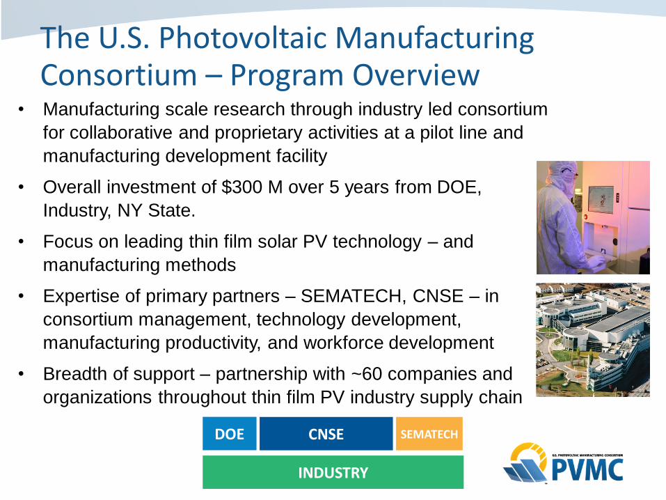
• Manufacturing scale research through industry led consortium
for collaborative and proprietary activities at a pilot line and
manufacturing development facility
• Overall investment of $300 M over 5 years from DOE,
Industry, NY State.
• Focus on leading thin film solar PV technology – and
manufacturing methods
• Expertise of primary partners – SEMATECH, CNSE – in
consortium management, technology development,
manufacturing productivity, and workforce development
• Breadth of support – partnership with ~60 companies and
organizations throughout thin film PV industry supply chain
The U.S. Photovoltaic Manufacturing Consortium – Program Overview
DOE CNSE SEMATECH
INDUSTRY

Strategic Objectives of PVMC
Establishing Roadmaps and Standards
Establishing Thin Film Manufacturing Development Facility
• Access to 100 kW line
• Front End and Back End of 10 MW
• (Flexible and Rigid Line)
Thin Film Manufacturing Scale-up
• Best Practices and Cost Modeling
• Productivity, Effectiveness and Manufacturing Quality
Thin Film Commercialization Support
• Deployment, Licensing, Attraction, Incubation
Developing Highly Trained Workforce
SOLICIT INDUSTRY INPUTS Design Projects
Results delivered according to milestones
Manufacturing scale up
Industry relevant projects ( LPV)
Metrology for Manufacturing
Performance measurement standards
Bankability
Outdoor performance Monitoring
Indoor Accelerated Life time tests
LPV
Metrology
Field Performance
TWG- Technical Working Groups

Yr1 Yr2 Yr3 Yr4 Yr5 Partners Objectives/Tasks
(FEOL) PV Cell Manufacturing
Equipment/Material Metrology/Suppliers, R&D Companies
Manufacturing Productivity, Cost Model, Metrology
(BEOL) Module Manufacturing
Equipment/Suppliers, PV and Roofing Manufacturers
Effectiveness, Life cycle, Reliability, Metrology Testing, Quality,
Roof Integration
Architects, Installers, Roofers, Contractors, Utilities
Design, Standards, Testing, Installation, Reliability, BOS
LPV Deployment
Utilities, Installer, End Users , Building Owners
Commercialization, Field Test, System Cost, Grid Integration
PVMC Multi-Year Strategy: 3 year and beyond

Current PVMC Members, Research Partners and Supply Partners
VersulfleX Technologies
6

Challenges in CIGS Reliability
7 22-Nov-13
To develop reliable PV modules Understand potential failure mechanisms driving a failure mode Reliability of a PV product depends on Manufacturing methods Types of packaging
Flat panel (Glass-Glass)-Monolithic Glass/Backsheet
Flexible modules (LPV) CPV
Used condition (climates) Observe failure modes (identify mechanisms) in outdoor PV field Need to wait for 25 years – NOT a solution! Develop accelerated stress tests-(and formulate Qualification tests) to observe the failure mechanisms in a short period of time to predict lifetime of the module

CIGS Device reliability Associated Failure modes/Mechanisms
Device/Unit film metrology TCO Engineering
8 22-Nov-13

CIGS device stack - Deposition methods and materials
9 25-Nov-13
XRR, AES, XPS
XRD
Substrate – Glass or foil
Back Contact – Mo
Absorber - CIGS
Buffer Layer – CdS
Window layer i-ZnO/(ITO or AZO)
Window layer: Sputter Resistive: i-ZnO-0.1-.12; Conductive:AZO- 0.1-.15
Buffer Layer: Chemical bath deposition (CBD) CdS, ~20-80nm;
CIGS: 1stage/2 stage /3 stage Cu, In, Ga are co-evaporated in Se overpressure CIGS- ~1-2
Molybdenum-Sputter; ~0.3-1 Barrier layers:Cr/Nitride
Glass:2mm or 3.2mm Stainless foil: ~25
Grids: Evaporation Ni (150-500A) Ag (5000-6000A) Al(2-3);
Dep
osi
tio
n m
eth
od
s &
Th
ickn
ess
Window layer: MoCVD
Zno:B; InZnO; ITO
Buffer Layer: Chemical bath deposition (CBD)/Sputter: Zn(O,S); ~20-80nm;
CIGS: Reactive sputtering, Ink deposition/ coating, Selenization, Co-evaporation
Grids/ Screen print/wire overlay/ tab and string
diff interconnects
Na barrier/ Se barrier/ Oxide barrier
Aluminum Polyimide
In-depth analysis using different characterization techniques is required to understand the interfacial properties-Include Na incorporation
Alternatives Co-evaporation example

Device efficiency- Moisture and Temperature/Light Effects
10
2) DH Degradation – Efficiency (0-50 hrs)- Encapsulated without EVA driven by decrease in Jsc & FF >10% Less than 5% decrease in Voc
Dark or l ight
d l
WV
TR
1
0
2
4
6
8
Y
1
2
0
2
4
6
8
Y
2
3
0
2
4
6
8
Y
3
4
0
2
4
6
8
Y
4
WV
TR
0 10 20 30 40 50
DH Exposure hours (h)
0 10 20 30 40 50
DH Exposure hours (h)
Y A Rs
Ov erlay Plot
Dark or l ight
d l
WV
TR
1
0
2
4
6
8
Y
1
2
0
2
4
6
8
Y
2
3
0
2
4
6
8
Y
3
4
0
2
4
6
8
Y
4
WV
TR
0 10 20 30 40 50
DH Exposure hours (h)
0 10 20 30 40 50
DH Exposure hours (h)
Y A Rs
Ov erlay Plot
Seri
es R
esis
tan
ce (
oh
ms
-cm
2)
Dio
de I
deality
Facto
r
Modeling of Dark and light JV curves
Parameters from Dark JV
-20
-10
0
10
Cha
nge
in E
ff[%
]
5004003002001000
Stress Time[hr]
B415_1
B47_1
B510_1
B517_1
0
4
8
12
16
20
1
0
4
8
12
16
20
Eff
icie
ncy
(%
)
2
0
4
8
12
16
20
3
0
4
8
12
16
20
4
wvtr
0 10 20 30 40 50
DH Exposure Hours (h)
Efficiency
0
4
8
12
16
20
1
0
4
8
12
16
20
Eff
icie
ncy
(%
)
2
0
4
8
12
16
20
3
0
4
8
12
16
20
4
wvtr
0 10 20 30 40 50
DH Exposure Hours (h)
Efficiency
Glass
Tefzel
Effi
cie
ncy
(%
)
Tefzel
Glass
1) CIS Device-Level Stability- D. Albin et.al 2) Influence of damp-heat in electrical, optical and morphological properties of encapsulated CIGS devices R.Sundaramoorthy et.al. 37th IEEE-PVSC
1
2
Dry with Light
Damp heat in Dark 2 Parameters from Light JV
Increase in R series for the cells packaged in back sheet with TEFZEL (high WVTR)
No change in R series for the cells packaged in back sheet with glass
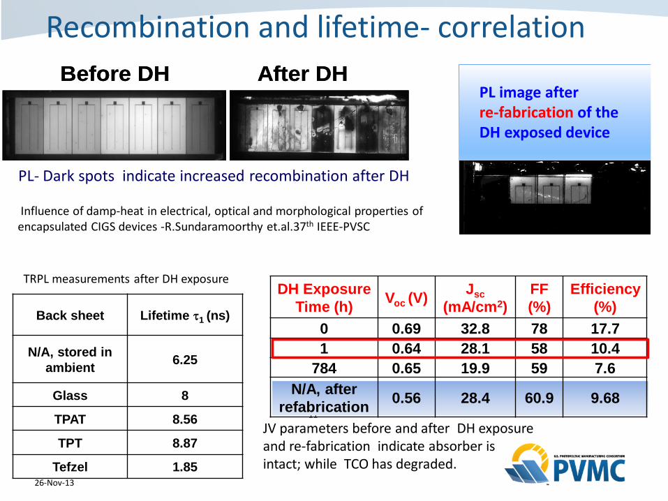
Recombination and lifetime- correlation
11
26-Nov-13
Before DH After DH
(a)
(b)
(c)
(d)
Before DH After DH
(a)
(b)
(c)
(d)
PL- Dark spots indicate increased recombination after DH
Back sheet Lifetime 1 (ns)
N/A, stored in
ambient 6.25
Glass 8
TPAT 8.56
TPT 8.87
Tefzel 1.85
DH Exposure
Time (h) Voc (V)
Jsc
(mA/cm2)
FF
(%)
Efficiency
(%)
0 0.69 32.8 78 17.7
1 0.64 28.1 58 10.4
784 0.65 19.9 59 7.6
N/A, after
refabrication 0.56 28.4 60.9 9.68
JV parameters before and after DH exposure and re-fabrication indicate absorber is intact; while TCO has degraded.
PL image after re-fabrication of the DH exposed device
Influence of damp-heat in electrical, optical and morphological properties of encapsulated CIGS devices -R.Sundaramoorthy et.al.37th IEEE-PVSC
TRPL measurements after DH exposure

529.9–530.7 eV
O 1s peak
(531.5–532.2 eV)
Zn(OH)2
(532.8–534 eV)
adsorbed water
Tefzel - High WVTR TPAT-Low WVTR
Oxygen 1s core level peak for samples encapsulated in
W. Eisele, et. al.Solar Energy Materials and Solar Cells 75, 2003, pp.17-23.
1
2
3 1
2
3
1
2
3
Material level –Identification of failure mechanisms
Evidence of hydrolysis of ZnO (TCO) and moisture in TCO Formation of Zn(OH)2 after DH exposure and moisture trapped in the devices packaged with backsheet having high WVTR

13
22-Nov-13
One approach for CIGS devices for improving device performance in DH Alternative TCO which is DH stable - IZO (InZnO) for CIGS
Conductive layer (i-ZnO/c-InZnO) Bi-layer(i-InZnO/c-InZnO)
Barrier layers on CIGS ( TCOs and PTMO)
TCO Engineering- device level
Soda lime Glass
Mo
CIGS
CdS i-ZnO
(AZO) Al:ZnO
Soda lime Glass
Mo
CIGS
CdS i-ZnO
(IZO) InZnO
CIGS devices with AZO
=16.6%
CIGS devices with IZO
=16.0% and 12.5%
R. Sundaramoorthy et.al 34th IEEE-PVSC Comparable efficiencies with alternative conducting
TCO which is DH stable
Un exposed After 38h in DH
PL Image after
DH exposure
PTMO protects the CIGS device
Extends the life time of the bare device- By how many hrs?
How is it related to lifetime during outdoor exposure
14 22-Nov-13
1
10
100
1000
10000
100000
1000000
0 50 100 150 200 250
DH Exposure Time (h)
Sh
eet
Resis
tan
ce (
oh
ms/s
q)
(a)
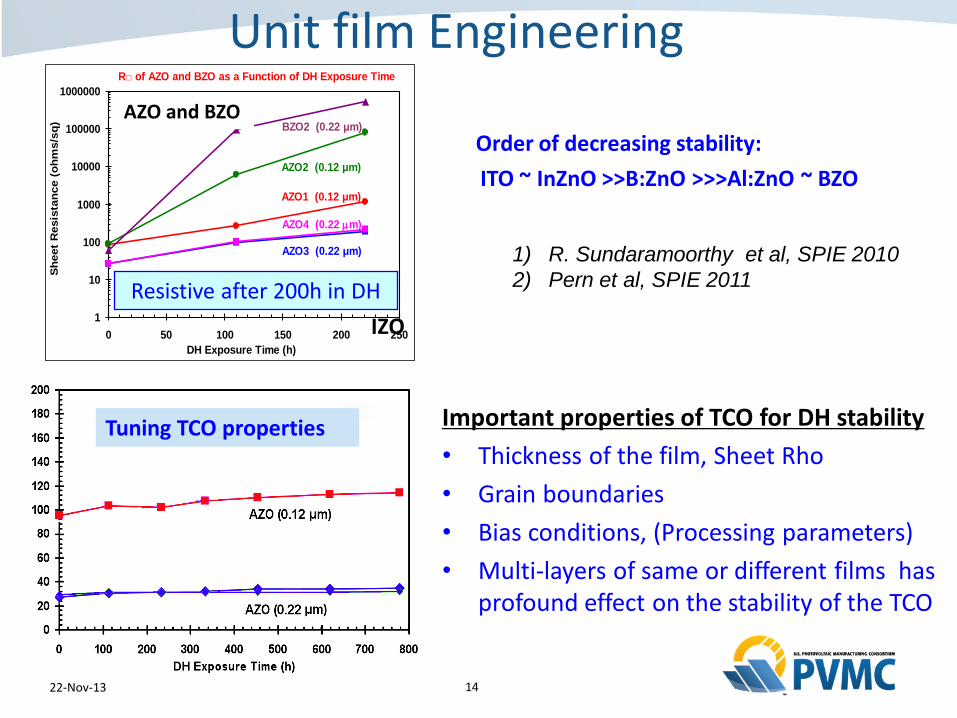
R□ of AZO and BZO as a Function of DH Exposure Time
AZO1 (0.12 μm)
AZO2 (0.12 μm)
AZO4 (0.22 m)
AZO3 (0.22 μm)
BZO2 (0.22 μm)
IZO
Resistive after 200h in DH
Order of decreasing stability:
ITO ~ InZnO >>B:ZnO >>>Al:ZnO ~ BZO
1) R. Sundaramoorthy et al, SPIE 2010
2) Pern et al, SPIE 2011
Unit film Engineering
Important properties of TCO for DH stability
• Thickness of the film, Sheet Rho
• Grain boundaries
• Bias conditions, (Processing parameters)
• Multi-layers of same or different films has profound effect on the stability of the TCO
AZO and BZO
Tuning TCO properties

Understand Long term reliability- CdS diffusion in CIGS failure mechanisms
• Failure physics correlated to mass transport kinetics
– Diffusion via lattice (volume)
– Diffusion via grain boundary
15 22-Nov-13
Grain Boundary Grain
Region 1 – Volume diffusion from the surface
Region 2 – Volume and grain boundary diffusion
Region 3 – Grain boundary diffusion
Region 4 – Background noise level
• SIMS analysis – – affected by Surface roughness
• Polish CIGS /Deposit CdS
The activation energy for volume diffusion of cadmium in CIGS is ~1 eV [2]
Thus ΔEb is ~0.7 eV ; Equation necessarily suggests ΔEb > ½ΔE
LaClaire’s analysis

Module level reliability Field failures
Indoor Accelerated Lifetime Tests (ALT’s) Interconnect reliability
Modeling
16 22-Nov-13

CIGS Module (Rigid/Flexible)
17 22-Nov-13
Deposition method Company
Co-evaporation Wurth, GSE, Ascent, Solibro
Selnenization Solar frontier, Avancis, STION , TSMC
Sputtering Miasole
Nanoparticle Nanosolar, ISET,-Pioneer products
Electroplating Solopower/NEXCIS
FASST and other process Heliovolt
Different ways of fabricating CIGS

Material Suppliers
Back contact and CIGS Processes
Buffer Layer (Toxic / Non Toxic)
Front Contact/Grids
Encapsulation materials and back end process
Module manufacturing
In the process of manufacturing a PV
module- each and every layer can be
processed in different ways-.Material
and equipment suppliers come up
with new products catering to different
process steps. Combination of all
these aspects makes the reliability of
the product challenging.

PVMRW2010-
John Wohlgemuth
Modules
in deserts
Silicone
encapsulant
- no glass
PVB encapsulants- with glass
Corrosion of metallization EVA IEC 61215 c-Si
1975 1976 1977 1978 1979
IEEE 1262
IQT
Thin film
product
IEC 61646
IEC61215
Qualification testing is confused with reliability testing
Incorporates pass/fail criteria- DOES NOT PREDIT PRODUCT LIFE TIME Stress levels and durations-limited- to minimize time and cost Goal: significant # of modules will pass the criteria- Production modules will be built the same way test modules are built.
Qual test for
Thin film PV
modules built around
c-Si PV failure
modes.
History of Qualification Tests –Certification Standards

TUV 1997-2011 Failure Rate Analysis of Module Design Qualification Testing - IV: 1997-2005 vs. 2005-2007 vs. 2007-2009 vs. 2009-2011; G. TamizhMani, et.al. TUV Rheinland PTL
New generation modules (‘05-’07)- DH failure rate 70% Lessons learnt (07-09) : • Brought down the
DH failure rate down to 30%
• New failure modes observed.
Questions: How do we replicate these failures in the lab?
Where does the failure occur in TF-PV?

Design differences
21 25-Nov-13
Tab and string
Monolithically integrated
Wire method
Design differences in modules can lead to different types of failure s in the field: ( Data from field : 203 modules and 53 designs) Hard failures (-20% to -85%) Pmax change due to FF Substring failure: (Voc loss) Delamination (Isc loss) Cell related loss and non-cell related loss Soft failures (10 to-20% ) Pmax change due to FF No dearth for interesting and useful topics to work on!
CNSE : Roof top Array
Design differences in current CIGS module manufacturing approach
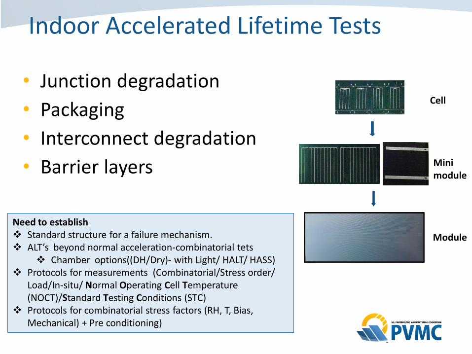
Indoor Accelerated Lifetime Tests
• Junction degradation
• Packaging
• Interconnect degradation
• Barrier layers
Cell
Mini module
Module
Need to establish Standard structure for a failure mechanism. ALT’s beyond normal acceleration-combinatorial tets
Chamber options((DH/Dry)- with Light/ HALT/ HASS) Protocols for measurements (Combinatorial/Stress order/
Load/In-situ/ Normal Operating Cell Temperature (NOCT)/Standard Testing Conditions (STC)
Protocols for combinatorial stress factors (RH, T, Bias, Mechanical) + Pre conditioning)

Effect of light, temperature and moisture
23
Effects of Light soak after DH exposure
Siemens Solar
Indoor : DH exposure with and without light exposure Degradation in the presence of light
is less than degradation in Dark -Damp heat
Effects of Temperature cycling / HF cycles
Effects of light on modules in DH chamber
K. Katsumi et..al
Showa Shell
Probable reason: Changes in the buffer layer due to the presence of moisture and heat could be the reason for decreased and improved performance the efficiency- failure mechanisms worth investigating
Indoor: Light Soak after DH exposure for 1000hrs Outdoor : Enhancement in efficiency by outdoor light soaking for 3-4 hrs after fabrication
Humidity freeze and Temperature cycles with no humidity shows similar changes in performance.
Future experiments
Isolate Temp. and Moisture and perform indoor tests with and without light to understand electrical performance
and compare the results with outdoor performance

Indoor ALT’s – Stress conditions- Multiple failure modes
24 22-Nov-13
85C
95C
Temperature and Humidity effects
Multiple failure modes High temperature : CIGS failure Low Temperatures : ECA dominated Failures Need to interpolate the results to use condition D.Coyle et.al PVMRW 2010
Combinations of different T and RH

Interconnect degradation Failure modes/mechanisms
25 22-Nov-13
J-V parameters
Voc , FF
Sheet resistance Mo-P3 scribe
Performance loss
Resistance P2 contact resistance
(Mo and ZnO:Al)
CIGS absorber
Enhanced recombination-due to defect density in
1)bulk or
2)at grain boundaries of CIGS
& Shift in the Fermi level CIGS/CdS interface
CC of ZnO:Al decreases
Affects FF ( high ohmic losses in Front contact)
ABSORBER
Monolithically interconnected cells

Finger prints-outdoor metrology & modeling
26
EDRX
Establishing a reliability methodology for thermal- cycle failure modes for CIGS modules-Kent Whitfield et.al.
Outdoor metrology Finger prints
“Deformation of the top bend is primarily driven by large expansion and contraction of the potting compound coupled with volumetric constraint offered by junction-box enclosure”
Failure mode and effect analysis Junction box, potting and busbar – stress/strain amplitude
Common Failure Modes for Thin-Film Modules and Considerations Toward Hardening CIGS Cells to Moisture -A “Suggested” Topic Kent Whitfield, Dir. Reliability
Correlation of metalling mixing corresponds to bond strength at the weld. a)Sharp b)smooth transitions in metal mixing
Welded joints analyzed using EDRX measurements .

Opportunities moving forward in CIGS reliability • Standards
– Develop standards ( light soak, Indoor tests- Find acceleration factors) – Develop standard test structures for analyzing different failure mechanisms
• Indoor ALT’s -Identify Failure modes and mechanisms
– Junction degradation ( Relate Cell- Module reliability) – Interconnect ( monolithic/cell based) – Packaging (Edge seal, EVA- Moisture ingress, PID) – Develop accelerated model
• Modeling
– Thermal cycling, Mechanical failures
• Outdoor field performance :
– Systematic metrology to understand field failures – Outdoor test individual modules and string outdoors in different climates and compare
with field data
• Relate Indoor testing – Outdoor testing- bridge the gap.
• Develop a web based reliability- bankability comprehensive database
27 22-Nov-13
Acknowledgment
• U.S. DOE’s Sun shot Initiative
• College of Nanoscale Science and Engineering (Albany)
• Photovoltaic Manufacturing consortium – Solar Energy development center (at Halfmoon NY)
28 22-Nov-13
THANK YOU FOR YOUR ATTENTION!