Embed Size (px)
Citation preview

LNK562-564LinkSwitch-LPEnergy Efficient Off-Line Switcher IC for Linear Transformer Replacement
Figure 1. Typical Application – not a Simplified Circuit (a) and Output Characteristic Envelope (b).
Product HighlightsLowest System Cost and Advanced Safety Features• Lowest component count switcher • Very tight parameter tolerances using proprietary IC
trimming technology and transformer construction techniques enable Clampless™designs – decreases component count/system cost and increases efficiency
• Meets industry standard requirements for thermal overload protection – eliminates the thermal fuse used with linear transformers or additional components in RCC designs
• Frequency jittering greatly reduces EMI – enables low cost input filter configuration
• Meets HV creepage requirements between DRAIN and all other pins, both on the PCB and at the package
• Proprietary E-Shield™ transformer eliminates Y capacitor
Superior Performance over Linear and RCC• Hysteretic thermal shutdown protection – automatic
recovery improves field reliability• Universal input range allows worldwide operation• Auto-restart reduces delivered power by >85% during
short circuit and open loop fault conditions • Simple ON/OFF control, no loop compensation needed• High bandwidth provides fast turn on with no overshoot
and excellent transient load response
EcoSmart®– Energy Efficiency Technology• Easily meets all global energy efficiency regulations with
no added components• No-load consumption <150 mW at 265 VAC input • ON/OFF control provides constant efficiency to very
light loads – ideal for mandatory CEC regulations
Applications• Chargers for cell/cordless phones, PDAs, power tools,
MP3/portable audio devices, shavers etc.• Standby and auxiliary supplies
DescriptionLinkSwitch-LP switcher ICs cost effectively replace all unregulated isolated linear transformer based (50/60 Hz) power supplies up to 3 W output power. For worldwide operation, a single universal input design replaces multiple linear transformer based designs. The self-biased circuit achieves an extremely low no-load consumption of under 150 mW. The internal oscillator
®
Table 1. Notes: 1. Output power may be limited by specific application parameters including core size and Clampless operation (see Key Application Considerations). 2. Minimum continuous power in a typical non-ventilated enclosed adapter measured at 50 °C ambient. 3. Minimum practical continuous power in an open frame design with adequate heat sinking, measured at 50 °C ambient. 4. Packages: P: DIP-8B, G: SMD-8B. For lead-free package options, see Part Ordering Information.
frequency is jittered to significantly reduce both quasi-peak and average EMI, minimizing filter cost.
October 2005
OUTPUT POWER TABLE1
PRODUCT4230 VAC ±15% 85-265 VAC
Adapter2 Open Frame3 Adapter2 Open
Frame3
LNK562P or G 1.9 W 1.9 W 1.9 W 1.9 WLNK563P or G 2.5 W 2.5 W 2.5 W 2.5 WLNK564P or G 3 W 3 W 3 W 3 W
IOIR
VR
VO
Adapter Rated OutputPower = VR • IR
PI-3924-101805
(a)
(b)
+
D
S
FB
BP
DCOutputAC
IN
LinkSwitch-LP
PI-3923-092705
2
LNK562-564
F10/05
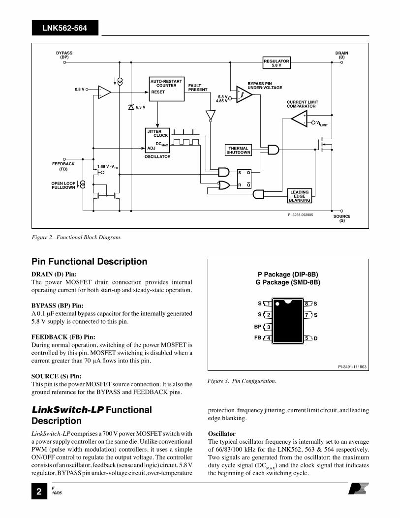
Figure 2. Functional Block Diagram.
Pin Functional DescriptionDRAIN (D) Pin:The power MOSFET drain connection provides internal operating current for both start-up and steady-state operation.
BYPASS (BP) Pin:A 0.1 μF external bypass capacitor for the internally generated 5.8 V supply is connected to this pin.
FEEDBACK (FB) Pin:During normal operation, switching of the power MOSFET is controlled by this pin. MOSFET switching is disabled when a current greater than 70 μA flows into this pin.
SOURCE (S) Pin:This pin is the power MOSFET source connection. It is also the ground reference for the BYPASS and FEEDBACK pins.
LinkSwitch-LP Functional DescriptionLinkSwitch-LP comprises a 700 V power MOSFET switch with a power supply controller on the same die. Unlike conventional PWM (pulse width modulation) controllers, it uses a simple ON/OFF control to regulate the output voltage. The controller consists of an oscillator, feedback (sense and logic) circuit, 5.8 V regulator, BYPASS pin under-voltage circuit, over-temperature
PI-3491-111903
FB D
S
BP
S
SS
P Package (DIP-8B)G Package (SMD-8B)
8
5
7
1
4
2
3
Figure 3. Pin Configuration.
protection, frequency jittering, current limit circuit, and leading edge blanking.
OscillatorThe typical oscillator frequency is internally set to an average of 66/83/100 kHz for the LNK562, 563 & 564 respectively. Two signals are generated from the oscillator: the maximum duty cycle signal (DCMAX) and the clock signal that indicates the beginning of each switching cycle.
PI-3958-092905
CLOCKJITTER
AUTO-RESTARTCOUNTER FAULT
PRESENT
OSCILLATOR
5.8 V4.85 V
SOURCE(S)
S
R
Q
DCMAXADJ
BYPASS(BP)
+
- VILIMIT
LEADINGEDGE
BLANKING
THERMALSHUTDOWN
+
-
DRAIN(D)
BYPASS PINUNDER-VOLTAGE
CURRENT LIMITCOMPARATOR
FEEDBACK(FB)
OPEN LOOPPULLDOWN Q
6.3 V
1.69 V -VTH
0.8 V+
REGULATOR5.8 V
RESET

3
LNK562-564
F10/05
The oscillator incorporates circuitry that introduces a small amount of frequency jitter, typically 5% of the switching frequency, to minimize EMI. The modulation rate of the frequency jitter is set to 1 kHz to optimize EMI reduction for both average and quasi-peak emissions. The frequency jitter, which is proportional to the oscillator frequency, should be measured with the oscilloscope triggered at the falling edge of the DRAIN voltage waveform. The waveform in Figure 4 illustrates the frequency jitter. The oscillator frequency is reduced when the FB pin voltage is less than 1.69 V as described below.
Feedback Input CircuitThe feedback input circuit at the FB pin consists of a low impedance source follower output set at 1.69 V. When the current delivered into this pin exceeds 70 μA, a low logic level (disable) is generated at the output of the feedback circuit. This output is sampled at the beginning of each cycle on the rising edge of the clock signal. If high, the power MOSFET is turned on for that cycle (enabled), otherwise the power MOSFET remains off (disabled). Since the sampling is done only at the beginning of each cycle, subsequent changes in the FB pin voltage or current during the remainder of the cycle are ignored. When the FB pin voltage falls below 1.69 V, the oscillator frequency linearly reduces to typically 48% at the auto-restart threshold voltage of 0.8 V. This function limits the power supply output current at output voltages below the rated voltage regulation threshold VR (see Figure 1).
5.8 V Regulator and 6.3 V Shunt Voltage ClampThe 5.8 V regulator charges the bypass capacitor connected to the BYPASS pin to 5.8 V by drawing a current from the voltage on the DRAIN, whenever the MOSFET is off. The BYPASS pin is the internal supply voltage node. When the MOSFET is on, the device runs off of the energy stored in the bypass capacitor. Extremely low power consumption of the internal circuitry allows LinkSwitch-LP to operate continuously from the current drawn from the DRAIN pin. A bypass capacitor value of 0.1 μF is sufficient for both high frequency decoupling and energy storage.
In addition, there is a 6.3 V shunt regulator clamping the BYPASS pin at 6.3 V when current is provided to the BYPASS pin externally. This facilitates powering the device externally through a resistor from the bias winding to decrease the no-load consumption.
BYPASS Pin Under-VoltageThe BYPASS pin under-voltage circuitry disables the power MOSFET when the BYPASS pin voltage drops below 4.85 V. Once the BYPASS pin voltage drops below 4.85 V, it must rise back to 5.8 V to enable (turn-on) the power MOSFET.
Over-Temperature ProtectionThe thermal shutdown circuitry senses the die temperature. The threshold is set at 142 °C typical with a 75 °C hysteresis. When the die temperature rises above this threshold (142 °C) the power MOSFET is disabled and remains disabled until the die temperature falls by 75 °C, at which point the MOSFET is re-enabled.
Current LimitThe current limit circuit senses the current in the power MOSFET. When this current exceeds the internal threshold (ILIMIT), the power MOSFET is turned off for the remainder of that cycle. The leading edge blanking circuit inhibits the current limit comparator for a short time (tLEB) after the power MOSFET is turned on. This leading edge blanking time has been set so that current spikes caused by capacitance and rectifier reverse recovery time will not cause premature termination of the MOSFET conduction.
Auto RestartIn the event of a fault condition such as output short circuit or an open loop condition, LinkSwitch-LP enters into auto-restart operation. An internal counter clocked by the oscillator gets reset every time the FB pin voltage exceeds the FEEDBACK Pin Auto-Restart Threshold Voltage (VFB(AR)). If the FB pin voltage drops below VFB(AR) for more than 100 ms, the power MOSFET switching is disabled. The auto-restart alternately enables and disables the switching of the power MOSFET at a duty cycle of typically 12% until the fault condition is removed.
Figure 4. Frequency Jitter at fOSC.
600
0 20
68 kHz64 kHz
VDRAIN
Time (µs)
PI-
3660
-081
303
500
400
300
200
100
0

4
LNK562-564
F10/05
Applications ExampleThe circuit shown in Figure 5 is a typical implementation of a 6 V, 330 mA, constant voltage, constant current (CV/CC) output power supply.
AC input differential filtering is accomplished with the very low cost input filter stage formed by C1 and L1. The proprietary frequency jitter feature of the LNK564 eliminates the need for an input pi filter, so only a single bulk capacitor is required. Adding a sleeve may allow the input inductor L1 to be used as a fuse as well as a filter component. This very simple Filterfuse™ input stage further reduces system cost. Alternatively, a fusible resistor RF1 may be used to provide the fusing function.
Input diode D2 may be removed from the neutral phase in applications where decreased EMI margins and/or decreased input surge withstand is allowed. In such applications, D1 will need to be an 800 V diode.
The power supply utilizes simplified bias winding voltage feedback, enabled by LNK564 ON/OFF control. The resistor divider formed by R1 and R2 determine the output voltage across the transformer bias winding during the switch OFF time. In the V/I constant voltage region, the LNK564 device enables/disables switching cycles to maintain 1.69 V on the FB pin. Diode D3 and low cost ceramic capacitor C3 provide rectification and filtering of the primary feedback winding waveform. At increased loads, beyond the constant power threshold, the FB pin voltage begins to reduce as the power supply output voltage falls. The internal oscillator frequency is linearly reduced in this region until it reaches typically 50% of the starting frequency. When the FB pin voltage drops below the auto-restart threshold (typically 0.8 V on the FB pin, which is equivalent to 1 V to 1.5 V at the
output of the power supply), the power supply will turn OFF for 800 ms and then turn back on for 100 ms. It will continue in this mode until the auto-restart threshold is exceeded. This function reduces the average output current during an output short circuit condition.
No-load consumption can be further reduced by increasing C3 to 0.47 μF or higher.
A Clampless primary circuit is achieved due to the very tight tolerance current limit trimming techniques used in manufacturing the LNK564, plus the transformer construction techniques used. Peak drain voltage is therefore limited to typically less than 550 V at 265 VAC, providing significant margin to the 700 V minimum drain voltage specification (BVDSS).
Output rectification and filtering is achieved with output rectifier D4 and filter capacitor C5. Due to the auto-restart feature, the average short circuit output current is significantly less than 1 A, allowing low cost rectifier D4 to be used. Output circuitry is designed to handle a continuous short circuit on the power supply output. Diode D4 is an ultra-fast type, selected for optimum V/I output characteristics. Optional resistor R3 provides a pre-load, limiting the output voltage level under no-load output conditions. Despite this pre-load, no-load consumption is within targets at approximately 140 mW at 265 VAC. The additional margin of no-load consumption requirement can be achieved by increasing the value of R4 to 2.2 kΩ or higher while still maintaining output voltage well below the 9 V maximum specification. Placement is left on the board for an optional Zener clamp (VR1) to limit maximum output voltage under open loop conditions, if required.
Figure 5. 6 V, 330 mA CV/CC Linear Replacement Power Supply.
D
S
FB
BP
J3-1
RTN
6 V,0.33 A
J3-2
L
J-1
J-2
N
D11N4937
RF1*8.2 Ω
2.5 WC1
10 µF400 V
C20.1 µF50 V
L13300 µH
D4UF4002
D31N4005
C5220 µF25 V
C3330 nF50 V
C4*100 pF
250 VAC
*Optional components
R32 kΩ
VR1*1N5240B
10 V
R23 kΩ
R137.4 kΩ
T1EE162
1
7
6
4
5D2
1N4005
90-265VAC
LinkSwitch-LP
PI-4106-101105
U1LNK564P

5
LNK562-564
F10/05
Key Application ConsiderationsOutput Power TableThe data sheet maximum output power table (Table 1) represents the maximum practical continuous output power level that can be obtained under the following assumed conditions:
1. The minimum DC input voltage is 90 V or higher for 85 VAC input, or 240 V or higher for 230 VAC input or 115 VAC with a voltage doubler. The value of the input capacitance should be large enough to meet these criteria for AC input designs.
2. Secondary output of 6 V with a Schottky rectifier diode.3. Assumed efficiency of 70%.4. Voltage only output (no secondary-side constant current
circuit).5. Discontinuous mode operation (KP > 1).6. A suitably sized core to allow a practical transformer design
(see Table 2).7. The part is board mounted with SOURCE pins soldered
to a sufficient area of copper to keep the SOURCE pin temperature at or below 100 °C.
8. Ambient temperature of 50 °C for open frame designs and an internal enclosure temperature of 60 °C for adapter designs.
Below a value of 1, KP is the ratio of ripple to peak primary current. Above a value of 1, KP is the ratio of primary MOSFET OFF time to the secondary diode conduction time. Due to the flux density requirements described below, typically a LinkSwitch-LP design will be discontinuous, which also has the benefit of allowing lower-cost fast (vs. ultra-fast) output diodes and reducing EMI.
Clampless DesignsClampless designs rely solely on the drain node capacitance to limit the leakage inductance induced peak drain-to-source voltage. Therefore the maximum AC input line voltage, the value of VOR, the leakage inductance energy, (a function of leakage inductance and peak primary current), and the primary winding capacitance determine the peak drain voltage. With no significant dissipative element present, as is the case with an external clamp, the longer duration of the leakage inductance ringing can increase EMI.
The following requirements are recommended for a universal input or 230 VAC only Clampless design:
1. Clampless designs should only be used for PO ≤ 2.5 W using a VOR of ≤ 90 V
2. For designs with PO ≤ 2 W, a two-layer primary must be used to ensure adequate primary intra-winding capacitance in the range of 25 pF to 50 pF.
3. For designs with 2 < PO ≤ 2.5 W, a bias winding must be added to the transformer using a standard recovery rectifier diode (1N4003– 1N4007) to act as a clamp. This bias winding may also be used to externally power the device by connecting a resistor from the bias winding capacitor to the BYPASS pin. This inhibits the internal high voltage current source, reducing device dissipation and no-load consumption.
4. For designs with PO > 2.5 W, Clampless designs are not practical and an external RCD or Zener clamp should be used.
5. Ensure that worst-case, high line, peak drain voltage is below the BVDSS specification of the internal MOSFET and ideally ≤ 650 V to allow margin for design variation.
VOR (Reflected Output Voltage), is the secondary output plus output diode forward voltage drop that is reflected to the primary via the turns ratio of the transformer during the diode conduction time. The VOR adds to the DC bus voltage and the leakage spike to determine the peak drain voltage.
Audible NoiseThe cycle skipping mode of operation used in LinkSwitch-LP can generate audio frequency components in the transformer. To limit this audible noise generation, the transformer should be designed such that the peak core flux density is below 1500 Gauss (150 mT). Following this guideline and using the standard transformer production technique of dip varnishing, practically eliminates audible noise. Vacuum impregnation of the transformer is not recommended, as it does not provide any better reduction of audible noise than dip varnishing. And although vacuum impregnation has the benefit of increased transformer capacitance (which helps in Clampless designs), it can also upset the mechanical design of the transformer, especially if shield windings are used. Higher flux densities are possible, increasing the power capability of the transformers above what is shown in Table 2. However careful evaluation of the audible noise performance should be made using production transformer samples before approving the design.
Ceramic capacitors that use dielectrics such as Z5U, when used in clamp circuits, may also generate audio noise. If this is the case, try replacing them with a capacitor having a different dielectric or construction, for example a film type.
Bias Winding FeedbackTo give the best output regulation in bias winding designs, a slow diode such as the 1N400x series should be used as the
LinkSwitch-LP DeviceCore Size LNK562 LNK563 LNK564
EE13 1.1 W 1.4 W 1.7 WEE16 1.3 W 1.7 W 2 WEE19 1.9 W 2.5 W 3 W
Table 2. Estimate of Transformer Power Capability vs. LinkSwitch-LP Device and Core Size at a Flux Density of 1500 Gauss (150 mT).

6
LNK562-564
F10/05
rectifier. This effectively filters the leakage inductance spike and reduces the error that this would give when using fast recovery time diodes. The use of a slow diode is a requirement in Clampless designs.
LinkSwitch-LP Layout Considerations
LayoutSee Figure 6 for a recommended circuit board layout for LinkSwitch-LP.
Single Point GroundingUse a single point ground connection from the input filter capacitor to the area of copper connected to the SOURCE pins.
Bypass Capacitor (CBP)The BYPASS pin capacitor should be located as near as possible to the BYPASS and SOURCE pins.
Primary Loop AreaThe area of the primary loop that connects the input filter capacitor, transformer primary and LinkSwitch-LP together should be kept as small as possible.
Primary Clamp CircuitAn external clamp may be used to limit peak voltage on the DRAIN pin at turn off. This can be achieved by using an RCD clamp or a Zener (~200 V) and diode clamp across the primary winding. In all cases, to minimize EMI, care should be taken to minimize the circuit path from the clamp components to the transformer and LinkSwitch-LP.
Thermal ConsiderationsThe copper area underneath the LinkSwitch-LP acts not only as a single point ground, but also as a heatsink. As it is connected to the quiet source node, this area should be maximized for good heat sinking of LinkSwitch-LP. The same applies to the cathode of the output diode.
+HV DCINPUT
-
+
Input FilterCapacitor
CBP
-
DCOUT
Output FilterCapacitor
PI-4157-101305
Maximize hatched copper areas ( ) for optimum heatsinking
TOP VIEW
T r a n s f o r m e r
Lin
kS
wit
ch
-LP
D
S
S
FB
BP
S
S
Y1-
Capacitor
Figure 6. Recommended Circuit Board Layout for LinkSwitch-LP (Assumes a HVDC Input Stage).

7
LNK562-564
F10/05
Y CapacitorThe placement of the Y capacitor should be directly from the primary input filter capacitor positive terminal to the common/return terminal of the transformer secondary. Such a placement will route high magnitude common-mode surge currents away from the LinkSwitch-LP device. Note: If an input pi (C, L, C) EMI filter is used, then the inductor in the filter should be placed between the negative terminals on the input filter capacitors.
Output DiodeFor best performance, the area of the loop connecting the secondary winding, the output diode and the output filter capacitor should be minimized. In addition, sufficient copper area should be provided at the anode and cathode terminals of the diode for heat sinking. A larger area is preferred at the quiet cathode terminal. A large anode area can increase high-frequency radiated EMI.
Quick Design Checklist
As with any power supply design, all LinkSwitch-LP designs should be verified on the bench to make sure that component specifications are not exceeded under worst-case conditions. The following minimum set of tests is strongly recommended:
1. Maximum drain voltage – Verify that VDS does not exceed 650 V at the highest input voltage and peak (overload) output power. A 50 V margin to the 700 V BVDSS specification gives margin for design variation, especially in Clampless designs.
2. Maximum drain current – At maximum ambient temperature, maximum input voltage and peak output (overload) power, verify drain current waveforms for any signs of transformer saturation and excessive leading-edge current spikes at startup. Repeat under steady state conditions and verify that the leading-edge current spike event is below ILIMIT(MIN) at the end of the tLEB(MIN). Under all conditions, the maximum DRAIN current should be below the specified absolute maximum ratings.
3. Thermal Check – At specified maximum output power, minimum input voltage and maximum ambient temperature, verify that the temperature specifications are not exceeded for LinkSwitch-LP, transformer, output diode and output capacitors. Enough thermal margin should be allowed for part-to-part variation of the RDS(ON) of LinkSwitch-LP as specified in the data sheet. Under low line and maximum power, a maximum LinkSwitch-LP SOURCE pin temperature of 100 °C is recommended to allow for these variations.
Design Tools
Up-to-date information on design tools can be found at the Power Integrations web site: www.powerint.com.

8
LNK562-564
F10/05
ABSOLUTE MAXIMUM RATINGS(1,6)
DRAIN Voltage .................................................. 700 V Peak DRAIN Current...................................200 mA (375 mA)(2) Peak Negative Pulsed Drain Current (see Fig. 10) ... 100 mA(3) FEEDBACK Voltage .........................................-0.3 V to 9 V FEEDBACK Current.............................................100 mA BYPASS Voltage ..........................................-0.3 V to 9 V Storage Temperature .......................................... -65 °C to 150 °C Operating Junction Temperature(4) ..................... -40 °C to 150 °C Lead Temperature(5) ........................................................260 °C
Notes: 1. All voltages referenced to SOURCE, TA = 25 °C. 2. The higher peak DRAIN current is allowed while the DRAIN voltage is simultaneously less than 400 V. 3. Duration not to exceed 2 μs. 4. Normally limited by internal circuitry. 5. 1/16 in. from case for 5 seconds. 6. Maximum ratings specified may be applied, one at a time, without causing permanent damage to the product. Exposure to Absolute Maximum Rating conditions for extended periods of time may affect product reliability.
THERMAL IMPEDANCEThermal Impedance: P or G Package: (θJA) ........................... 70 °C/W(2); 60 °C/W(3)
(θJC)(1) ............................................... 11 °C/W
Notes: 1. Measured on pin 2 (SOURCE) close to plastic interface. 2. Soldered to 0.36 sq. in. (232 mm2), 2 oz. (610 g/m2) copper clad. 3. Soldered to 1 sq. in. (645 mm2), 2 oz. (610 g/m2) copper clad.
Parameter SymbolConditions
SOURCE = 0 V; TJ = -40 to 125 °C See Figure 7
(Unless Otherwise Specified)
Min Typ Max Units
CONTROL FUNCTIONS
Output Frequency fOSC
TJ = 25 °C VFB =1.69 V Average
LNK562 61 66 71kHzLNK563 77 83 89
LNK564 93 100 107
Ratio of Output Frequency At Auto-Restart to fOSC
fOSC(AR) TJ = 25 °C, VFB = VFB(AR) 48 %
Frequency Jitter Peak-Peak Jitter, TJ = 25 °C 5 %
Maximum Duty Cycle DCMAX S2 Open 66 70 %
FEEDBACK Pin Turnoff Threshold Current
IFBTJ = 25 °C See Note A 56 70 84 μA
FEEDBACK Pin Voltage at Turnoff Threshold
VFBTJ = 0 to 125 °C
See Note A 1.60 1.69 1.78 V
DRAIN Supply Current
IS1
VFB ≥ 2 V (MOSFET Not Switching)
See Note B160 220 μA
IS2
FEEDBACK Open (MOSFET Switching)
See Notes B, C220 260 μA

9
LNK562-564
F10/05
Parameter SymbolConditions
SOURCE = 0 V; TJ = -40 to 125 °C See Figure 7
(Unless Otherwise Specified)
Min Typ Max Units
CONTROL FUNCTIONS (cont.)BYPASS Pin Charge Current
ICH1 VBP = 0 V, TJ = 25 °C, See Note D -5.5 -3.3 -1.8mA
ICH2 VBP = 4 V, TJ = 25 °C, See Note D -3.8 -2.3 -1.0
BYPASS Pin Voltage VBP 5.55 5.8 6.10 V
BYPASS Pin Voltage Hysteresis VBPH 0.8 0.95 1.2 V
BYPASS Pin Supply Current IBPSC See Note E 84 μA
CIRCUIT PROTECTION
Current Limit ILIMIT di/dt = 40 mA/μs
TJ = 25 °C 124 136 148 mA
Power Coefficient I2f di/dt = 40 mA/μs TJ = 25 °C
LNK562 1099 1221 1380A2HzLNK563 1381 1535 1735
LNK564 1665 1850 2091
Leading Edge Blanking Time tLEB
TJ = 25 °C See Note F 220 265 ns
Thermal Shutdown Temperature TSD 135 142 150 °C
Thermal Shutdown Hysteresis TSHD See Note G 75 °C
OUTPUTON-State Resistance RDS(ON) ID = 13 mA
TJ = 25 °C 48 55Ω
TJ = 100 °C 76 88
OFF-State Drain Leakage Current IDSS
VBP = 6.2 V, VFB ≥2 V, VDS = 560 V, TJ = 25 °C 50 μA
Breakdown Voltage BVDSSVBP = 6.2 V, VFB ≥2 V,
See Note H, TJ = 25 °C 700 V
DRAIN Supply Voltage 50 V
Output Enable Delay tEN See Figure 9 17 μs
Output Disable Setup Time tDST 0.5 μs

10
LNK562-564
F10/05
Parameter SymbolConditions
SOURCE = 0 V; TJ = -40 to 125 °C See Figure 7
(Unless Otherwise Specified)
Min Typ Max Units
OUTPUT (cont.)FEEDBACK Pin Auto-Restart Threshold Voltage
VFB(AR) TJ = 25 °C 0.8 V
Auto-Restart ON-Time
VFB = VFB(AR) TJ = 25 °C 100 ms
Auto-Restart Duty Cycle DCAR 12 %
NOTES:A. In a scheme using a resistor divider network at the FB pin, where RU is the resistor from the FB pin to the rectified
bias voltage and RL is the resistor from the FB pin to the SOURCE pin, the output voltage variation is influenced by VFB and IFB variations. To determine the contribution from the VFB variation in percent, the following equation can be used:
To determine the contribution from IFB variation in percent, the following equation can be used:
Since IFB and VFB are independent parameters, the composite variation in percent would be .
B. Total current consumption is the sum of IS1 and IDSS when FEEDBACK pin voltage is ≥2 V (MOSFET not switching) and the sum of IS2 and IDSS when FEEDBACK pin is shorted to SOURCE (MOSFET switching).
C Since the output MOSFET is switching, it is difficult to isolate the switching current from the supply current at the DRAIN. An alternative is to measure the BYPASS pin current at 6 V.
D. See Typical Performance Characteristics section Figure 15 for BYPASS pin start-up charging waveform.
E. This current is only intended to supply an optional optocoupler connected between the BYPASS and FEEDBACK pins and not any other external circuitry.
F. This parameter is guaranteed by design.
G. This parameter is derived from characterization.
H. Breakdown voltage may be checked against minimum BVDSS by ramping the DRAIN pin voltage up to but not exceeding minimum BVDSS.
V RR R I R
V RR R I R
x 100 1( ) ( )
( ) ( )
FB TYPL
U LFB TYP U
FB MAXL
U LFB TYP U
#=+
+
++
-
J
L
KKKK b
bN
P
OOOOl
l
V RR R I R
V RR R I R
y 100 1( ) ( )
( ) ( )
FB TYPL
U LFB TYP U
FB TYPL
U LFB MAX U
#=+
+
++
-
J
L
KKKK b
bN
P
OOOOl
l
x y2 2! +
11
LNK562-564
F10/05
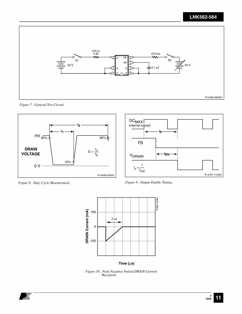
Figure 7. General Test Circuit.
PI-3490-060204
50 V50 V
D FB
SS
S S
BPS1
470 kΩ
S2
0.1 µF
470 Ω5 W
PI-3707-112503
FB
tP
tEN
DCMAX
tP =
1
fOSC
VDRAIN
(internal signal)
Figure 8. Duty Cycle Measurement. Figure 9. Output Enable Timing.
0
100
Time (µs)
DR
AIN
Cu
rren
t (m
A) PI-
4021
-101
305
-100
2 µs
Figure 10. Peak Negative Pulsed DRAIN Current Waveform.

12
LNK562-564
F10/05
1.4
1.0
1.2
0.8
0.6
0.4
0.2
0-50 0 50 100 150
Temperature (°C)
PI-
4164
-100
505
Cu
rren
t L
imit
(No
rmal
ized
to
25
°C)
100
150
175
200
125
00 42 86 10 12 14 16 18 20
DRAIN Voltage (V)
DR
AIN
Cu
rren
t (m
A) PI-
3927
-083
104
25
75
50
25 °C100 °C
Typical Performance Characteristics
Figure 15. BYPASS Pin Start-up Waveform.
1.1
1.0
0.9-50 -25 0 25 50 75 100 125 150
Junction Temperature (°C)
Bre
akd
ow
n V
olt
age
(No
rmal
ized
to
25
°C) PI-
2213
-012
301
6
5
4
3
2
1
0
0 0.2 0.4 0.6 0.8 1.0
Time (ms)
PI-
2240
-012
301
BY
PA
SS
Pin
Vo
ltag
e (V
)
7
Figure 11. Breakdown vs. Temperature.
Figure 13. Current Limit vs. Temperature.
Figure 16. Output Characteristics.
1.2
1.0
0.8
0.6
0.4
0.2
0-50 -25 0 25 50 75 100 125
Junction Temperature (°C)
PI-
2680
-012
301
Ou
tpu
t F
req
uen
cy(N
orm
aliz
ed t
o 2
5 °C
)
Figure 12. Frequency vs. Temperature.
1.1
1.0
0.9-50 -25 0 25 50 75 100 125 150
Temperature (°C)
FE
ED
BA
CK
Pin
Vo
ltag
e(N
orm
aliz
ed t
o 2
5 °C
) PI-
4057
-071
905
Figure 14. FEEDBACK Pin Voltage vs. Temperature.

13
LNK562-564
F10/05
Figure 17. COSS vs. Drain Voltage.
Drain Voltage (V)
Dra
in C
apac
itan
ce (
pF
)
PI-
3928
-083
104
0 100 200 300 400 500 600
1
10
100
1000
Typical Performance Characteristics (cont.)
PART ORDERING INFORMATIONLinkSwitch Product FamilyLP Series NumberPackage Identifier
G Plastic Surface Mount DIPP Plastic DIP
Lead FinishN Pure Matte Tin (Pb-Free)
Tape & Reel and Other OptionsBlank Standard Configurations
TL Tape & Reel, 1000 pcs minimum, G package onlyLNK 562 G N - TL

14
LNK562-564
F10/05
Notes:1. Package dimensions conform to JEDEC specification MS-001-AB (Issue B 7/85) for standard dual-in-line (DIP) package with .300 inch row spacing.2. Controlling dimensions are inches. Millimeter sizes are shown in parentheses.3. Dimensions shown do not include mold flash or other protrusions. Mold flash or protrusions shall not exceed .006 (.15) on any side.4. Pin locations start with Pin 1, and continue counter-clock- wise to Pin 8 when viewed from the top. The notch and/or dimple are aids in locating Pin 1. Pin 6 is omitted.5. Minimum metal to metal spacing at the package body for the omitted lead location is .137 inch (3.48 mm).6. Lead width measured at package body. 7. Lead spacing measured with the leads constrained to be perpendicular to plane T.
.008 (.20)
.015 (.38)
.300 (7.62) BSC(NOTE 7)
.300 (7.62)
.390 (9.91)
.367 (9.32)
.387 (9.83)
.240 (6.10)
.260 (6.60)
.125 (3.18)
.145 (3.68)
.057 (1.45)
.068 (1.73)
.120 (3.05)
.140 (3.56)
.015 (.38)MINIMUM
.048 (1.22)
.053 (1.35).100 (2.54) BSC
.014 (.36)
.022 (.56)
-E-
Pin 1
SEATINGPLANE
-D-
-T-
P08B
DIP-8B
PI-2551-121504
D S .004 (.10)⊕
T E D S .010 (.25) M⊕
(NOTE 6)
.137 (3.48) MINIMUM
SMD-8B
PI-2546-121504
.004 (.10)
.012 (.30).036 (0.91).044 (1.12)
.004 (.10)
0 - ° 8°
.367 (9.32)
.387 (9.83)
.048 (1.22).009 (.23)
.053 (1.35).032 (.81).037 (.94)
.125 (3.18)
.145 (3.68)
-D-
Notes:1. Controlling dimensions are inches. Millimeter sizes are shown in parentheses.2. Dimensions shown do not include mold flash or other protrusions. Mold flash or protrusions shall not exceed .006 (.15) on any side.3. Pin locations start with Pin 1, and continue counter-clock- wise to Pin 8 when viewed from the top. Pin 6 is omitted.4. Minimum metal to metal spacing at the package body for the omitted lead location is .137 inch (3.48 mm).5. Lead width measured at package body. 6. D and E are referenced datums on the package body.
.057 (1.45)
.068 (1.73)(NOTE 5)
E S
.100 (2.54) (BSC)
.372 (9.45).240 (6.10)
.388 (9.86)
.137 (3.48) MINIMUM
.260 (6.60).010 (.25)
-E-
Pin 1
D S .004 (.10)⊕
⊕
G08B
.420
.046 .060 .060 .046
.080Pin 1
.086.186
.286
Solder Pad Dimensions

15
LNK562-564
F10/05

16
LNK562-564
F10/05
Revision Notes DateE 1) Final Release Data Sheet 10/05F 2) Revision of PI-3924 10/05
For the latest updates, visit our website: www.powerint.comPower Integrations reserves the right to make changes to its products at any time to improve reliability or manufacturability. Power Integrations does not assume any liability arising from the use of any device or circuit described herein. POWER INTEGRATIONS MAKES NO WARRANTY HEREIN AND SPECIFICALLY DISCLAIMS ALL WARRANTIES INCLUDING, WITHOUT LIMITATION, THE IMPLIED WARRANTIES OF MERCHANTABILITY, FITNESS FOR A PARTICULAR PURPOSE, AND NON-INFRINGEMENT OF THIRD PARTY RIGHTS.
PATENT INFORMATION
The products and applications illustrated herein (including transformer construction and circuits external to the products) may be covered by one or more U.S. and foreign patents, or potentially by pending U.S. and foreign patent applications assigned to Power Integrations. A complete list of Power Integrations patents may be found at www.powerint.com. Power Integrations grants its customers a license under certain patent rights as set forth at http://www.powerint.com/ip.htm.
LIFE SUPPORT POLICY
POWER INTEGRATIONS PRODUCTS ARE NOT AUTHORIZED FOR USE AS CRITICAL COMPONENTS IN LIFE SUPPORT DEVICES OR SYSTEMS WITHOUT THE EXPRESS WRITTEN APPROVAL OF THE PRESIDENT OF POWER INTEGRATIONS. As used herein:
1. A Life support device or system is one which, (i) is intended for surgical implant into the body, or (ii) supports or sustains life, and (iii) whose failure to perform, when properly used in accordance with instructions for use, can be reasonably expected to result in significant injury or death to the user.
2. A critical component is any component of a life support device or system whose failure to perform can be reasonably expected to cause the failure of the life support device or system, or to affect its safety or effectiveness.
The PI logo, TOPSwitch, TinySwitch, LinkSwitch, DPA-Switch, EcoSmart, Clampless, E-Shield, Filterfuse, PI Expert and PI FACTS are trademarks of Power Integrations, Inc. Other trademarks are property of their respective companies. ©Copyright 2005, Power Integrations, Inc.
Power Integrations Worldwide Sales Support LocationsWORLD HEADQUARTERS5245 Hellyer AvenueSan Jose, CA 95138, USA.Main: +1-408-414-9200Customer Service: Phone: +1-408-414-9665Fax: +1-408-414-9765e-mail: [email protected]
CHINA (SHANGHAI)Rm 807-808A Pacheer Commercial Centre,555 Nanjing Rd. West Shanghai, P.R.C. 200041Phone: +86-21-6215-5548Fax: +86-21-6215-2468e-mail: [email protected]
CHINA (SHENZHEN)Rm 2206-2207, Block A,Electronics Science & Technology Bldg.2070 Shennan Zhong Rd. Shenzhen, Guangdong,China, 518031Phone: +86-755-8379-3243Fax: +86-755-8379-5828e-mail: [email protected]
GERMANY Rueckertstrasse 3D-80336, Munich GermanyPhone: +49-89-5527-3910Fax: +49-89-5527-3920e-mail: [email protected]
INDIA261/A, Ground Floor7th Main, 17th Cross,SadashivanagarBangalore, India 560080 Phone: +91-80-5113-8020Fax: +91-80-5113-8023e-mail: [email protected]
ITALYVia Vittorio Veneto 12 20091 Bresso MIItalyPhone: +39-028-928-6000Fax: +39-028-928-6009e-mail: [email protected]
JAPANKeihin Tatemono 1st Bldg 2-12-20 Shin-Yokohama, Kohoku-ku, Yokohama-shi, Kanagawa ken, Japan 222-0033Phone: +81-45-471-1021Fax: +81-45-471-3717e-mail: [email protected]
KOREARM 602, 6FLKorea City Air Terminal B/D, 159-6Samsung-Dong, Kangnam-Gu,Seoul, 135-728, KoreaPhone: +82-2-2016-6610Fax: +82-2-2016-6630e-mail: [email protected]
SINGAPORE 51 Newton Road#15-08/10 Goldhill PlazaSingapore, 308900Phone: +65-6358-2160Fax: +65-6358-2015e-mail: [email protected]
TAIWAN5F, No. 318, Nei Hu Rd., Sec. 1 Nei Hu Dist.Taipei, Taiwan 114, R.O.C.Phone: +886-2-2659-4570Fax: +886-2-2659-4550e-mail: [email protected]
EUROPE HQ1st Floor, St. Jamesʼs HouseEast Street, FarnhamSurrey GU9 7TJUnited KingdomPhone: +44 (0) 1252-730-140Fax: +44 (0) 1252-727-689 e-mail: [email protected]
APPLICATIONS HOTLINE World Wide +1-408-414-9660
APPLICATIONS FAX World Wide +1-408-414-9760