Embed Size (px)
Citation preview
Contents
Features ..............................................................1Applications .........................................................1Pin Assignment ...................................................1Block Diagram .....................................................2Selection Guide ...................................................2Output Configurations..........................................5Absolute Maximum Ratings .................................6Electrical Characteristics .....................................7Test Circuits ........................................................11Technical Terms..................................................12Standard Circuit...................................................13Operation.............................................................14Dimensions..........................................................16Taping ................................................................17Marking ...............................................................20Characteristics (typical characteristics)................21Application Circuit Examples ...............................28Remarks..............................................................29Frequently Asked Questions................................30
Seiko Instruments Inc. 1
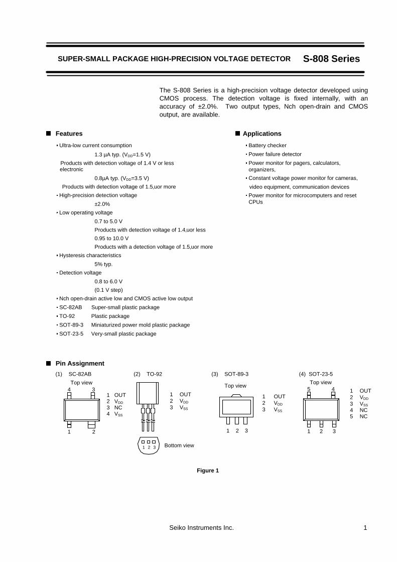
SUPER-SMALL PACKAGE HIGH-PRECISION VOLTAGE DETECTOR S-808 Series
The S-808 Series is a high-precision voltage detector developed usingCMOS process. The detection voltage is fixed internally, with anaccuracy of ±2.0%. Two output types, Nch open-drain and CMOSoutput, are available.
Features
Ultra-low current consumption
1.3 µA typ. (VDD=1.5 V)
Products with detection voltage of 1.4 V or lesselectronic
0.8µA typ. (VDD=3.5 V)
Products with detection voltage of 1.5‚uor more
High-precision detection voltage
±2.0%
Low operating voltage
0.7 to 5.0 V
Products with detection voltage of 1.4‚uor less
0.95 to 10.0 V
Products with a detection voltage of 1.5‚uor more
Hysteresis characteristics
5% typ.
Detection voltage
0.8 to 6.0 V
(0.1 V step)
Nch open-drain active low and CMOS active low output
SC-82AB Super-small plastic package
TO-92 Plastic package
SOT-89-3 Miniaturized power mold plastic package
SOT-23-5 Very-small plastic package
Pin Assignment
(1) SC-82AB (2) TO-92 (3) SOT-89-3 (4) SOT-23-5
Applications
Battery checker
Power failure detector
Power monitor for pagers, calculators,organizers,
Constant voltage power monitor for cameras,
video equipment, communication devices
Power monitor for microcomputers and resetCPUs
Top view
1 2 3
1 2 3 Bottom view
1 OUT2 VDD
3 VSS
Top view5 4
321
1 OUT2 VDD
3 NC4 VSS
4 3
21
1 OUT2 VDD
3 VSS
1 OUT2 VDD
3 VSS
4 NC5 NC
Figure 1
Top view
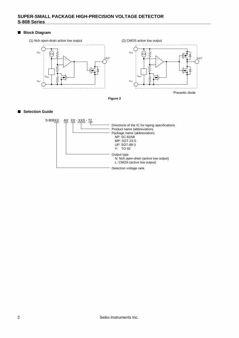
SUPER-SMALL PACKAGE HIGH-PRECISION VOLTAGE DETECTORS-808 Series
2 Seiko Instruments Inc.
Block Diagram
(1) Nch open-drain active low output (2) CMOS active low output
OUT
VREF
VSS
−
+
VDD
*
OUT
VREF
VSS
VDD
*
*
−
+
*Parasitic diode
Figure 2
Selection Guide
S-808XX AX XX - XXX - T2
Output typeN: Nch open-drain (active low output)L: CMOS (active low output)
Detection voltage rank
Package name (abbreviation)NP: SC-82ABMP: SOT-23-5UP: SOT-89-3Y: TO-92
Product name (abbreviation)Directions of the IC for taping specifications

SUPER-SMALL PACKAGE HIGH-PRECISION VOLTAGE DETECTOR S-808 Series
Seiko Instruments Inc. 3
Table 1
Detection voltage range Hysteresis width Nch Open Drain(Low)(V) VHYS typ.(V) SC-82AB TO-92 SOT-89-3 SOT-23-5
0.8V±2.0% 0.034 S-80808ANNP-E7Y-T2 — — —
0.9V±2.0% 0.044 S-80809ANNP-E7Z-T2 — — —
1.0V±2.0% 0.054 S-80810ANNP-E70-T2 — — —
1.1V±2.0% 0.064 S-80811ANNP-E71-T2 — — —
1.2V±2.0% 0.073 S-80812ANNP-E72-T2 — — —
1.3V±2.0% 0.083 S-80813ANNP-EDA-T2 — — —
1.4V±2.0% 0.093 S-80814ANNP-EDB-T2 — — —
1.5V±2.0% 0.075 S-80815ANNP-EDC-T2 S-80815ANY S-80815ANUP-EDC-T2 —
1.6V±2.0% 0.080 S-80816ANNP-EDD-T2 S-80816ANY S-80816ANUP-EDD-T2 —
1.7V±2.0% 0.085 S-80817ANNP-EDE-T2 S-80817ANY S-80817ANUP-EDE-T2 S-80817ANMP-EDE-T2
1.8V±2.0% 0.090 S-80818ANNP-EDF-T2 S-80818ANY S-80818ANUP-EDF-T2 S-80818ANMP-EDF-T2
1.9V±2.0% 0.095 S-80819ANNP-EDG-T2 S-80819ANY S-80819ANUP-EDG-T2 S-80819ANMP-EDG-T2
2.0V±2.0% 0.100 S-80820ANNP-EDH-T2 S-80820ANY S-80820ANUP-EDH-T2 S-80820ANMP-EDH-T2
2.1V±2.0% 0.105 S-80821ANNP-EDJ-T2 S-80821ANY S-80821ANUP-EDJ-T2 S-80821ANMP-EDJ-T2
2.2V±2.0% 0.110 S-80822ANNP-EDK-T2 S-80822ANY S-80822ANUP-EDK-T2 S-80822ANMP-EDK-T2
2.3V±2.0% 0.115 S-80823ANNP-EDL-T2 S-80823ANY S-80823ANUP-EDL-T2 S-80823ANMP-EDL-T2
2.4V±2.0% 0.120 S-80824ANNP-EDM-T2 S-80824ANY S-80824ANUP-EDM-T2 S-80824ANMP-EDM-T2
2.5V±2.0% 0.125 S-80825ANNP-EDN-T2 S-80825ANY S-80825ANUP-EDN-T2 S-80825ANMP-EDN-T2
2.6V±2.0% 0.130 S-80826ANNP-EDP-T2 S-80826ANY S-80826ANUP-EDP-T2 —
2.7V±2.0% 0.135 S-80827ANNP-EDQ-T2 S-80827ANY S-80827ANUP-EDQ-T2 S-80827ANMP-EDQ-T2
2.8V±2.0% 0.140 S-80828ANNP-EDR-T2 S-80828ANY S-80828ANUP-EDR-T2 S-80828ANMP-EDR-T2
2.9V±2.0% 0.145 S-80829ANNP-EDS-T2 S-80829ANY S-80829ANUP-EDS-T2 —
3.0V±2.0% 0.150 S-80830ANNP-EDT-T2 S-80830ANY S-80830ANUP-EDT-T2 S-80830ANMP-EDT-T2
3.1V±2.0% 0.155 S-80831ANNP-EDV-T2 S-80831ANY S-80831ANUP-EDV-T2 —
3.2V±2.0% 0.160 S-80832ANNP-EDW-T2 S-80832ANY S-80832ANUP-EDW-T2 S-80832ANMP-EDW-T2
3.3V±2.0% 0.165 S-80833ANNP-EDX-T2 S-80833ANY S-80833ANUP-EDX-T2 S-80833ANMP-EDX-T2
3.4V±2.0% 0.170 S-80834ANNP-EDY-T2 S-80834ANY S-80834ANUP-EDY-T2 S-80834ANMP-EDY-T2
3.5V±2.0% 0.175 S-80835ANNP-EDZ-T2 S-80835ANY S-80835ANUP-EDZ-T2 S-80835ANMP-EDZ-T2
3.6V±2.0% 0.180 S-80836ANNP-ED0-T2 S-80836ANY S-80836ANUP-ED0-T2 S-80836ANMP-ED0-T2
3.7V±2.0% 0.185 S-80837ANNP-ED1-T2 S-80837ANY S-80837ANUP-ED1-T2 —
3.8V±2.0% 0.190 S-80838ANNP-ED2-T2 S-80838ANY S-80838ANUP-ED2-T2 —
3.9V±2.0% 0.195 S-80839ANNP-ED3-T2 S-80839ANY S-80839ANUP-ED3-T2 S-80839ANMP-ED3-T2
4.0V±2.0% 0.200 S-80840ANNP-ED4-T2 S-80840ANY S-80840ANUP-ED4-T2 S-80840ANMP-ED4-T2
4.1V±2.0% 0.205 S-80841ANNP-ED5-T2 S-80841ANY S-80841ANUP-ED5-T2 —
4.2V±2.0% 0.210 S-80842ANNP-ED6-T2 S-80842ANY S-80842ANUP-ED6-T2 S-80842ANMP-ED6-T2
4.3V±2.0% 0.215 S-80843ANNP-ED7-T2 S-80843ANY S-80843ANUP-ED7-T2 —
4.4V±2.0% 0.220 S-80844ANNP-ED8-T2 S-80844ANY S-80844ANUP-ED8-T2 S-80844ANMP-ED8-T2
4.5V±2.0% 0.225 S-80845ANNP-ED9-T2 S-80845ANY S-80845ANUP-ED9-T2 S-80845ANMP-ED9-T2
4.6V±2.0% 0.230 S-80846ANNP-EJA-T2 S-80846ANY S-80846ANUP-EJA-T2 —
4.7V±2.0% 0.235 S-80847ANNP-EJB-T2 S-80847ANY S-80847ANUP-EJB-T2 —
4.8V±2.0% 0.240 S-80848ANNP-EJC-T2 S-80848ANY S-80848ANUP-EJC-T2 —
4.9V±2.0% 0.245 S-80849ANNP-EJD-T2 S-80849ANY S-80849ANUP-EJD-T2 —
5.0V±2.0% 0.250 S-80850ANNP-EJE-T2 S-80850ANY S-80850ANUP-EJE-T2 S-80850ANMP-EJE-T2
5.1V±2.0% 0.255 S-80851ANNP-EJF-T2 S-80851ANY S-80851ANUP-EJF-T2 S-80851ANMP-EJF-T2
5.2V±2.0% 0.260 S-80852ANNP-EJG-T2 — S-80852ANUP-EJG-T2 —
5.3V±2.0% 0.265 S-80853ANNP-EJH-T2 S-80853ANY — —
5.4V±2.0% 0.270 S-80854ANNP-EJJ-T2 — — —
5.5V±2.0% 0.275 S-80855ANNP-EJK-T2 — — —
5.6V±2.0% 0.280 S-80856ANNP-EJL-T2 — — —
5.7V±2.0% 0.285 S-80857ANNP-EJM-T2 — — —
5.8V±2.0% 0.290 S-80858ANNP-EJN-T2 — — —
5.9V±2.0% 0.295 S-80859ANNP-EJP-T2 — — —
6.0V±2.0% 0.300 S-80860ANNP-EJQ-T2 — S-80860ANUP-EJQ-T2 —
SUPER-SMALL PACKAGE HIGH-PRECISION VOLTAGE DETECTORS-808 Series
4 Seiko Instruments Inc.
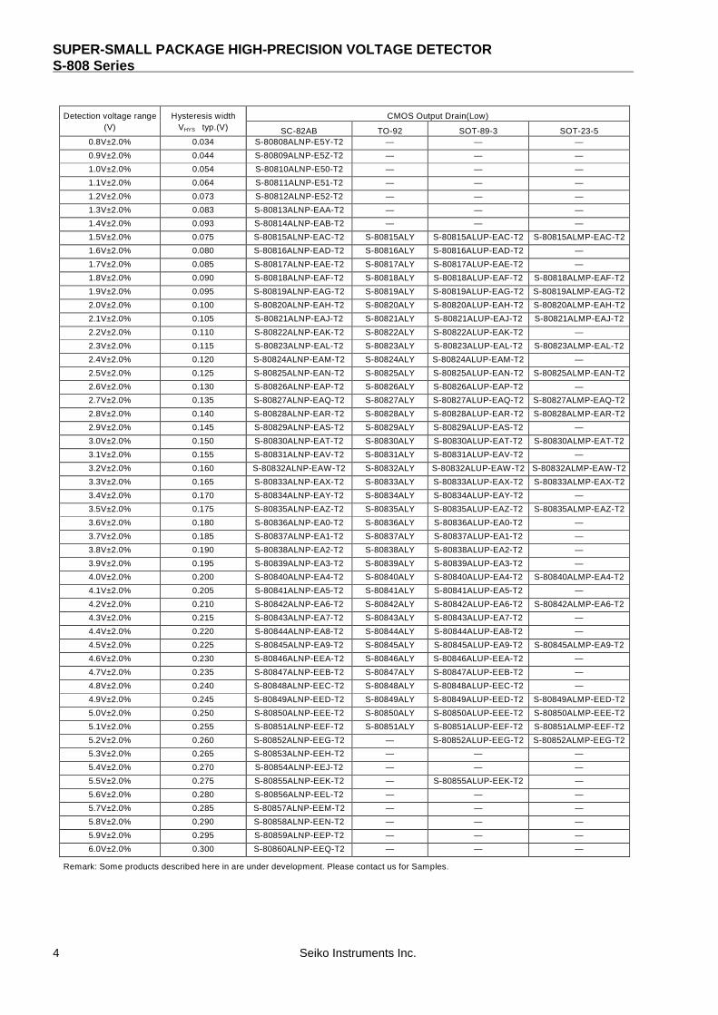
Detection voltage range Hysteresis width CMOS Output Drain(Low)(V) VHYS typ.(V) SC-82AB TO-92 SOT-89-3 SOT-23-5
0.8V±2.0% 0.034 S-80808ALNP-E5Y-T2 — — —
0.9V±2.0% 0.044 S-80809ALNP-E5Z-T2 — — —
1.0V±2.0% 0.054 S-80810ALNP-E50-T2 — — —
1.1V±2.0% 0.064 S-80811ALNP-E51-T2 — — —
1.2V±2.0% 0.073 S-80812ALNP-E52-T2 — — —
1.3V±2.0% 0.083 S-80813ALNP-EAA-T2 — — —
1.4V±2.0% 0.093 S-80814ALNP-EAB-T2 — — —
1.5V±2.0% 0.075 S-80815ALNP-EAC-T2 S-80815ALY S-80815ALUP-EAC-T2 S-80815ALMP-EAC-T2
1.6V±2.0% 0.080 S-80816ALNP-EAD-T2 S-80816ALY S-80816ALUP-EAD-T2 —
1.7V±2.0% 0.085 S-80817ALNP-EAE-T2 S-80817ALY S-80817ALUP-EAE-T2 —
1.8V±2.0% 0.090 S-80818ALNP-EAF-T2 S-80818ALY S-80818ALUP-EAF-T2 S-80818ALMP-EAF-T2
1.9V±2.0% 0.095 S-80819ALNP-EAG-T2 S-80819ALY S-80819ALUP-EAG-T2 S-80819ALMP-EAG-T2
2.0V±2.0% 0.100 S-80820ALNP-EAH-T2 S-80820ALY S-80820ALUP-EAH-T2 S-80820ALMP-EAH-T2
2.1V±2.0% 0.105 S-80821ALNP-EAJ-T2 S-80821ALY S-80821ALUP-EAJ-T2 S-80821ALMP-EAJ-T2
2.2V±2.0% 0.110 S-80822ALNP-EAK-T2 S-80822ALY S-80822ALUP-EAK-T2 —
2.3V±2.0% 0.115 S-80823ALNP-EAL-T2 S-80823ALY S-80823ALUP-EAL-T2 S-80823ALMP-EAL-T2
2.4V±2.0% 0.120 S-80824ALNP-EAM-T2 S-80824ALY S-80824ALUP-EAM-T2 —
2.5V±2.0% 0.125 S-80825ALNP-EAN-T2 S-80825ALY S-80825ALUP-EAN-T2 S-80825ALMP-EAN-T2
2.6V±2.0% 0.130 S-80826ALNP-EAP-T2 S-80826ALY S-80826ALUP-EAP-T2 —
2.7V±2.0% 0.135 S-80827ALNP-EAQ-T2 S-80827ALY S-80827ALUP-EAQ-T2 S-80827ALMP-EAQ-T2
2.8V±2.0% 0.140 S-80828ALNP-EAR-T2 S-80828ALY S-80828ALUP-EAR-T2 S-80828ALMP-EAR-T2
2.9V±2.0% 0.145 S-80829ALNP-EAS-T2 S-80829ALY S-80829ALUP-EAS-T2 —
3.0V±2.0% 0.150 S-80830ALNP-EAT-T2 S-80830ALY S-80830ALUP-EAT-T2 S-80830ALMP-EAT-T2
3.1V±2.0% 0.155 S-80831ALNP-EAV-T2 S-80831ALY S-80831ALUP-EAV-T2 —
3.2V±2.0% 0.160 S-80832ALNP-EAW-T2 S-80832ALY S-80832ALUP-EAW-T2 S-80832ALMP-EAW-T2
3.3V±2.0% 0.165 S-80833ALNP-EAX-T2 S-80833ALY S-80833ALUP-EAX-T2 S-80833ALMP-EAX-T2
3.4V±2.0% 0.170 S-80834ALNP-EAY-T2 S-80834ALY S-80834ALUP-EAY-T2 —
3.5V±2.0% 0.175 S-80835ALNP-EAZ-T2 S-80835ALY S-80835ALUP-EAZ-T2 S-80835ALMP-EAZ-T2
3.6V±2.0% 0.180 S-80836ALNP-EA0-T2 S-80836ALY S-80836ALUP-EA0-T2 —
3.7V±2.0% 0.185 S-80837ALNP-EA1-T2 S-80837ALY S-80837ALUP-EA1-T2 —
3.8V±2.0% 0.190 S-80838ALNP-EA2-T2 S-80838ALY S-80838ALUP-EA2-T2 —
3.9V±2.0% 0.195 S-80839ALNP-EA3-T2 S-80839ALY S-80839ALUP-EA3-T2 —
4.0V±2.0% 0.200 S-80840ALNP-EA4-T2 S-80840ALY S-80840ALUP-EA4-T2 S-80840ALMP-EA4-T2
4.1V±2.0% 0.205 S-80841ALNP-EA5-T2 S-80841ALY S-80841ALUP-EA5-T2 —
4.2V±2.0% 0.210 S-80842ALNP-EA6-T2 S-80842ALY S-80842ALUP-EA6-T2 S-80842ALMP-EA6-T2
4.3V±2.0% 0.215 S-80843ALNP-EA7-T2 S-80843ALY S-80843ALUP-EA7-T2 —
4.4V±2.0% 0.220 S-80844ALNP-EA8-T2 S-80844ALY S-80844ALUP-EA8-T2 —
4.5V±2.0% 0.225 S-80845ALNP-EA9-T2 S-80845ALY S-80845ALUP-EA9-T2 S-80845ALMP-EA9-T2
4.6V±2.0% 0.230 S-80846ALNP-EEA-T2 S-80846ALY S-80846ALUP-EEA-T2 —
4.7V±2.0% 0.235 S-80847ALNP-EEB-T2 S-80847ALY S-80847ALUP-EEB-T2 —
4.8V±2.0% 0.240 S-80848ALNP-EEC-T2 S-80848ALY S-80848ALUP-EEC-T2 —
4.9V±2.0% 0.245 S-80849ALNP-EED-T2 S-80849ALY S-80849ALUP-EED-T2 S-80849ALMP-EED-T2
5.0V±2.0% 0.250 S-80850ALNP-EEE-T2 S-80850ALY S-80850ALUP-EEE-T2 S-80850ALMP-EEE-T2
5.1V±2.0% 0.255 S-80851ALNP-EEF-T2 S-80851ALY S-80851ALUP-EEF-T2 S-80851ALMP-EEF-T2
5.2V±2.0% 0.260 S-80852ALNP-EEG-T2 — S-80852ALUP-EEG-T2 S-80852ALMP-EEG-T2
5.3V±2.0% 0.265 S-80853ALNP-EEH-T2 — — —
5.4V±2.0% 0.270 S-80854ALNP-EEJ-T2 — — —
5.5V±2.0% 0.275 S-80855ALNP-EEK-T2 — S-80855ALUP-EEK-T2 —
5.6V±2.0% 0.280 S-80856ALNP-EEL-T2 — — —
5.7V±2.0% 0.285 S-80857ALNP-EEM-T2 — — —
5.8V±2.0% 0.290 S-80858ALNP-EEN-T2 — — —
5.9V±2.0% 0.295 S-80859ALNP-EEP-T2 — — —
6.0V±2.0% 0.300 S-80860ALNP-EEQ-T2 — — —
Remark: Some products described here in are under development. Please contact us for Samples.

SUPER-SMALL PACKAGE HIGH-PRECISION VOLTAGE DETECTOR S-808 Series
Seiko Instruments Inc. 5
Output Configurations
1. S-808 Series model numbering system
Nch open-drain(“L” reset type)
CMOS output(“L” reset type)
S-808 Series“N” is the last letter of themodel number.e.g. S-80808AN
“L” is the last letter of themodel number.e.g. S-80808AL
2. Output configurations and their implementation
Implementation Nch(“L” ) CMOS(“L” )
With different power supplies Yes NoWith active low reset CPUs Yes YesWith active high reset CPUs No NoWith voltage divider variable resistors Yes No
Example with two power supplies Examples with one power supply
VSS
OUTCPU
VDD2VDD1
V/DNch
VSS
OUTCPU
VDD2VDD1
V/DCMOS
VSS
OUTCPU
VDD2VDD1
V/DNch
Figure 3
SUPER-SMALL PACKAGE HIGH-PRECISION VOLTAGE DETECTORS-808 Series
6 Seiko Instruments Inc.
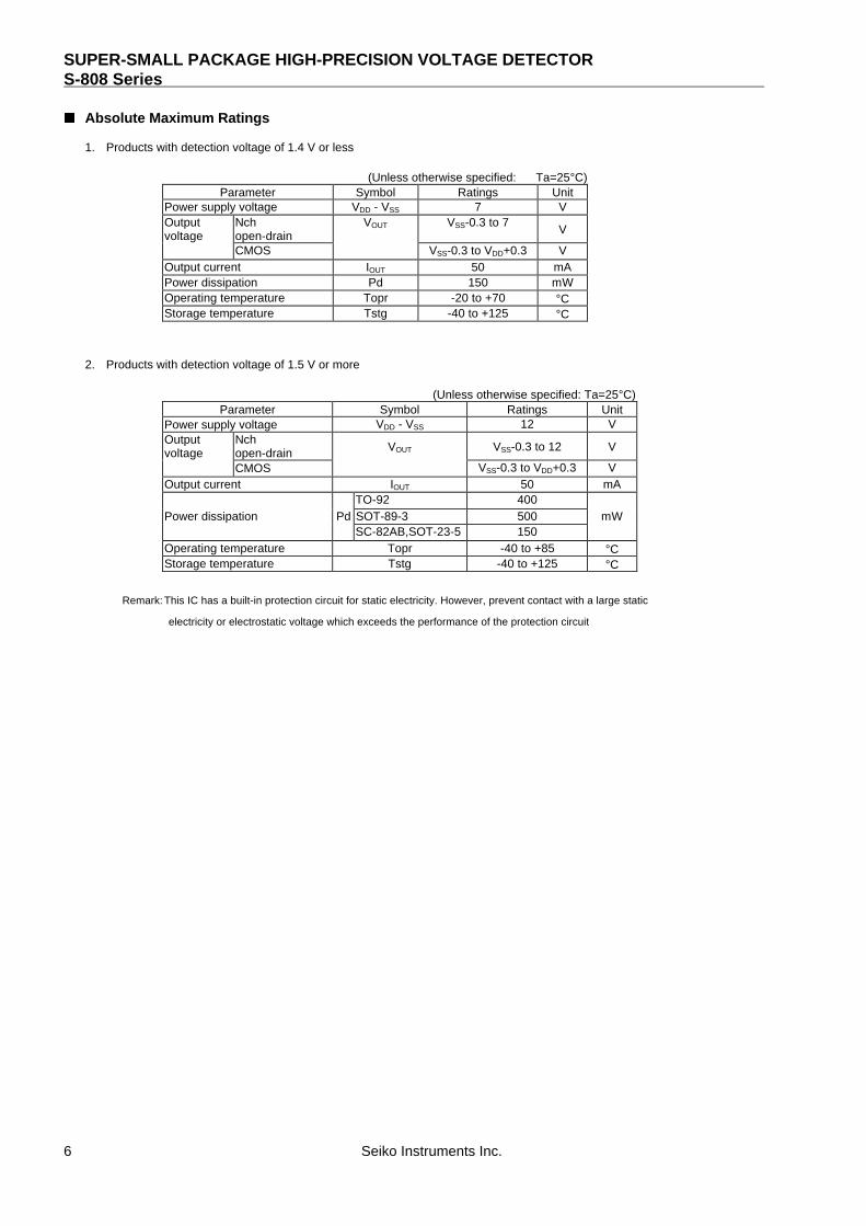
Absolute Maximum Ratings
1. Products with detection voltage of 1.4 V or less
(Unless otherwise specified: Ta=25°C)Parameter Symbol Ratings Unit
Power supply voltage VDD - VSS 7 VOutputvoltage
Nchopen-drain
VOUT VSS-0.3 to 7V
CMOS VSS-0.3 to VDD+0.3 VOutput current IOUT 50 mAPower dissipation Pd 150 mWOperating temperature Topr -20 to +70 °CStorage temperature Tstg -40 to +125 °C
2. Products with detection voltage of 1.5 V or more
(Unless otherwise specified: Ta=25°C)Parameter Symbol Ratings Unit
Power supply voltage VDD - VSS 12 VOutputvoltage
Nchopen-drain VOUT VSS-0.3 to 12 V
CMOS VSS-0.3 to VDD+0.3 VOutput current IOUT 50 mA
TO-92 400Power dissipation Pd SOT-89-3 500 mW
SC-82AB,SOT-23-5 150Operating temperature Topr -40 to +85 °CStorage temperature Tstg -40 to +125 °C
Remark:This IC has a built-in protection circuit for static electricity. However, prevent contact with a large static
electricity or electrostatic voltage which exceeds the performance of the protection circuit

SUPER-SMALL PACKAGE HIGH-PRECISION VOLTAGE DETECTOR S-808 Series
Seiko Instruments Inc. 7
Electrical Characteristics
1. Detection voltage (0.8 V to 1.4 V)
(Unless otherwise specified: Ta=25°C)
Parameter Symbol Conditions Min. Typ. Max. UnitTest
circuit
S-80808AX 0.784 0.800 0.816
S-80809AX 0.882 0.900 0.918
S-80810AX 0.980 1.000 1.020
Detection voltage -VDET S-80811AX 1.078 1.100 1.122 V 1
S-80812AX 1.176 1.200 1.224
S-80813AX 1.274 1.300 1.326
S-80814AX 1.372 1.400 1.428
S-80808AX 0.802 0.834 0.867
S-80809AX 0.910 0.944 0.979
S-80810AX 1.017 1.054 1.091
Release voltage +VDET S-80811AX 1.125 1.164 1.203 V 1
S-80812AX 1.232 1.273 1.315
S-80813AX 1.340 1.383 1.427
S-80814AX 1.448 1.493 1.538
S-80808AX 0.018 0.034 0.051
S-80809AX 0.028 0.044 0.061
S-80810AX 0.037 0.054 0.071
Hysteresis width VHYS S-80811AX 0.047 0.064 0.081 V 1
S-80812AX 0.056 0.073 0.091
S-80813AX 0.066 0.083 0.101
S-80814AX 0.076 0.093 0.110
VDD=1.5V S-80808AX
S-80809AX
S-80810AX
CurrentISS
S-80811AX — 1.3 3.7 µA 2consumption
VDD=2.0V S-80812AX
S-80813AX
S-80814AX
Operating voltage VDD 0.7 — 5.0 V 1
Nch VDS=0.5V 0.04 0.2 — 3
Output current IOUT VDD=0.7V mA
Pch(CMOS VDS=2.1V 2.9 5.8 — 4
output) VDD=4.5V
Leakage current ofoutput transistor ILEAK
Nch(Nchopen drain)
VDS=5.0VVDD=5.0V — —
60 nA 3
S-80808AX — ±0.18 —S-80809AX — ±0.20 —
Temperature ∆-VDET Ta=-20°C S-80810AX — ±0.22 — mV/°C 1
characteristic of ∆Ta to +70°C S-80811AX — ±0.24 —
-VDET S-80812AX — ±0.27 —S-80813AX — ±0.29 —S-80814AX — ±0.31 —
SUPER-SMALL PACKAGE HIGH-PRECISION VOLTAGE DETECTORS-808 Series
8 Seiko Instruments Inc.
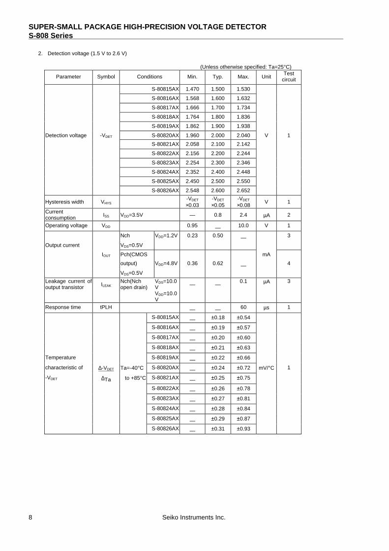
2. Detection voltage (1.5 V to 2.6 V)
(Unless otherwise specified: Ta=25°C)
Parameter Symbol Conditions Min. Typ. Max. UnitTest
circuit
S-80815AX 1.470 1.500 1.530
S-80816AX 1.568 1.600 1.632
S-80817AX 1.666 1.700 1.734
S-80818AX 1.764 1.800 1.836
S-80819AX 1.862 1.900 1.938
Detection voltage -VDET S-80820AX 1.960 2.000 2.040 V 1
S-80821AX 2.058 2.100 2.142
S-80822AX 2.156 2.200 2.244
S-80823AX 2.254 2.300 2.346
S-80824AX 2.352 2.400 2.448
S-80825AX 2.450 2.500 2.550
S-80826AX 2.548 2.600 2.652
Hysteresis width VHYS-VDET
×0.03-VDET
×0.05-VDET
×0.08V 1
Currentconsumption ISS VDD=3.5V — 0.8 2.4 µA 2
Operating voltage VDD 0.95 — 10.0 V 1
Nch VDD=1.2V 0.23 0.50 — 3
Output current VDS=0.5V
IOUT Pch(CMOS mA
output) VDD=4.8V 0.36 0.62 — 4
VDS=0.5V
Leakage current ofoutput transistor ILEAK
Nch(Nchopen drain)
VDS=10.0VVDD=10.0V
— —0.1 µA 3
Response time tPLH — — 60 µs 1
S-80815AX — ±0.18 ±0.54
S-80816AX — ±0.19 ±0.57
S-80817AX — ±0.20 ±0.60
S-80818AX — ±0.21 ±0.63
Temperature S-80819AX — ±0.22 ±0.66
characteristic of ∆-VDET Ta=-40°C S-80820AX — ±0.24 ±0.72 mV/°C 1
-VDET ∆Ta to +85°C S-80821AX — ±0.25 ±0.75
S-80822AX — ±0.26 ±0.78
S-80823AX — ±0.27 ±0.81
S-80824AX — ±0.28 ±0.84
S-80825AX — ±0.29 ±0.87
S-80826AX — ±0.31 ±0.93
SUPER-SMALL PACKAGE HIGH-PRECISION VOLTAGE DETECTOR S-808 Series
Seiko Instruments Inc. 9
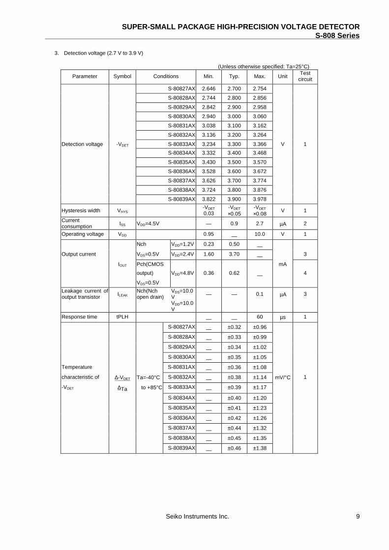
3. Detection voltage (2.7 V to 3.9 V)
(Unless otherwise specified: Ta=25°C)
Parameter Symbol Conditions Min. Typ. Max. UnitTest
circuit
S-80827AX 2.646 2.700 2.754
S-80828AX 2.744 2.800 2.856
S-80829AX 2.842 2.900 2.958
S-80830AX 2.940 3.000 3.060
S-80831AX 3.038 3.100 3.162
S-80832AX 3.136 3.200 3.264
Detection voltage -VDET S-80833AX 3.234 3.300 3.366 V 1
S-80834AX 3.332 3.400 3.468
S-80835AX 3.430 3.500 3.570
S-80836AX 3.528 3.600 3.672
S-80837AX 3.626 3.700 3.774
S-80838AX 3.724 3.800 3.876
S-80839AX 3.822 3.900 3.978
Hysteresis width VHYS-VDET
0.03-VDET
×0.05-VDET
×0.08V 1
Currentconsumption ISS VDD=4.5V — 0.9 2.7 µA 2
Operating voltage VDD 0.95 — 10.0 V 1
Nch VDD=1.2V 0.23 0.50 —Output current VDS=0.5V VDD=2.4V 1.60 3.70 — 3
IOUT Pch(CMOS mA
output) VDD=4.8V 0.36 0.62 — 4
VDS=0.5V
Leakage current ofoutput transistor ILEAK
Nch(Nchopen drain)
VDS=10.0VVDD=10.0V
— — 0.1 µA 3
Response time tPLH — — 60 µs 1
S-80827AX — ±0.32 ±0.96
S-80828AX — ±0.33 ±0.99
S-80829AX — ±0.34 ±1.02
S-80830AX — ±0.35 ±1.05
Temperature S-80831AX — ±0.36 ±1.08
characteristic of ∆-VDET Ta=-40°C S-80832AX — ±0.38 ±1.14 mV/°C 1
-VDET ∆Ta to +85°C S-80833AX — ±0.39 ±1.17
S-80834AX — ±0.40 ±1.20
S-80835AX — ±0.41 ±1.23
S-80836AX — ±0.42 ±1.26
S-80837AX — ±0.44 ±1.32
S-80838AX — ±0.45 ±1.35
S-80839AX — ±0.46 ±1.38
SUPER-SMALL PACKAGE HIGH-PRECISION VOLTAGE DETECTORS-808 Series
10 Seiko Instruments Inc.
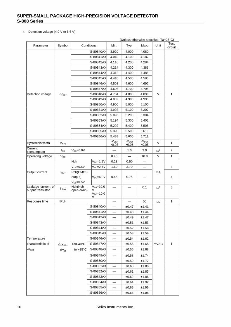
4. Detection voltage (4.0 V to 5.6 V)
(Unless otherwise specified: Ta=25°C)
Parameter Symbol Conditions Min. Typ. Max. UnitTest
circuitS-80840AX 3.920 4.000 4.080
S-80841AX 4.018 4.100 4.182
S-80842AX 4.116 4.200 4.284
S-80843AX 4.214 4.300 4.386
S-80844AX 4.312 4.400 4.488
S-80845AX 4.410 4.500 4.590
S-80846AX 4.508 4.600 4.692
S-80847AX 4.606 4.700 4.794
Detection voltage -VDET S-80848AX 4.704 4.800 4.896 V 1
S-80849AX 4.802 4.900 4.998
S-80850AX 4.900 5.000 5.100
S-80851AX 4.998 5.100 5.202
S-80852AX 5.096 5.200 5.304
S-80853AX 5.194 5.300 5.406
S-80854AX 5.292 5.400 5.508
S-80855AX 5.390 5.500 5.610
S-80856AX 5.488 5.600 5.712
Hysteresis width VHYS-VDET
×0.03-VDET
×0.05-VDET
×0.08 V 1
Currentconsumption ISS VDD=6.0V — 1.0 3.0 µA 2
Operating voltage VDD 0.95 — 10.0 V 1
Nch VDD=1.2V 0.23 0.50 —
VDS=0.5V VDD=2.4V 1.60 3.70 — 3
Output current IOUT Pch(CMOS mA
output) VDD=6.0V 0.46 0.75 — 4
VDS=0.5V
Leakage current ofoutput transistor ILEAK
Nch(Nchopen drain)
VDS=10.0VVDD=10.0V
— — 0.1 µA 3
Response time tPLH — — 60 µs 1
S-80840AX — ±0.47 ±1.41
S-80841AX — ±0.48 ±1.44
S-80842AX — ±0.49 ±1.47
S-80843AX — ±0.51 ±1.53
S-80844AX — ±0.52 ±1.56
S-80845AX — ±0.53 ±1.59
Temperature S-80846AX — ±0.54 ±1.62
characteristic of ∆-VDET Ta=-40°C S-80847AX — ±0.55 ±1.65 mV/°C 1
-VDET ∆Ta to +85°C S-80848AX — ±0.56 ±1.68
S-80849AX — ±0.58 ±1.74
S-80850AX — ±0.59 ±1.77
S-80851AX — ±0.60 ±1.80
S-80852AX — ±0.61 ±1.83
S-80853AX — ±0.62 ±1.86
S-80854AX — ±0.64 ±1.92
S-80855AX — ±0.65 ±1.95
S-80856AX — ±0.66 ±1.98
SUPER-SMALL PACKAGE HIGH-PRECISION VOLTAGE DETECTOR S-808 Series
Seiko Instruments Inc. 11
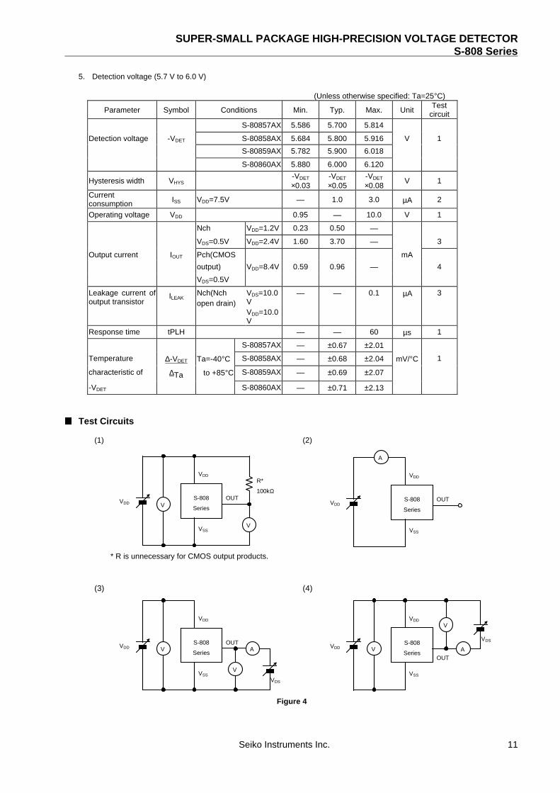
5. Detection voltage (5.7 V to 6.0 V)
(Unless otherwise specified: Ta=25°C)
Parameter Symbol Conditions Min. Typ. Max. UnitTest
circuitS-80857AX 5.586 5.700 5.814
Detection voltage -VDET S-80858AX 5.684 5.800 5.916 V 1
S-80859AX 5.782 5.900 6.018
S-80860AX 5.880 6.000 6.120
Hysteresis width VHYS-VDET
×0.03-VDET
×0.05-VDET
×0.08V 1
Currentconsumption ISS VDD=7.5V — 1.0 3.0 µA 2
Operating voltage VDD 0.95 — 10.0 V 1
Nch VDD=1.2V 0.23 0.50 —
VDS=0.5V VDD=2.4V 1.60 3.70 — 3
Output current IOUT Pch(CMOS mA
output) VDD=8.4V 0.59 0.96 — 4
VDS=0.5V
Leakage current ofoutput transistor
ILEAKNch(Nchopen drain)
VDS=10.0VVDD=10.0V
— — 0.1 µA 3
Response time tPLH — — 60 µs 1
S-80857AX — ±0.67 ±2.01
Temperature ∆-VDET Ta=-40°C S-80858AX — ±0.68 ±2.04 mV/°C 1
characteristic of ∆Ta to +85°C S-80859AX — ±0.69 ±2.07
-VDET S-80860AX — ±0.71 ±2.13
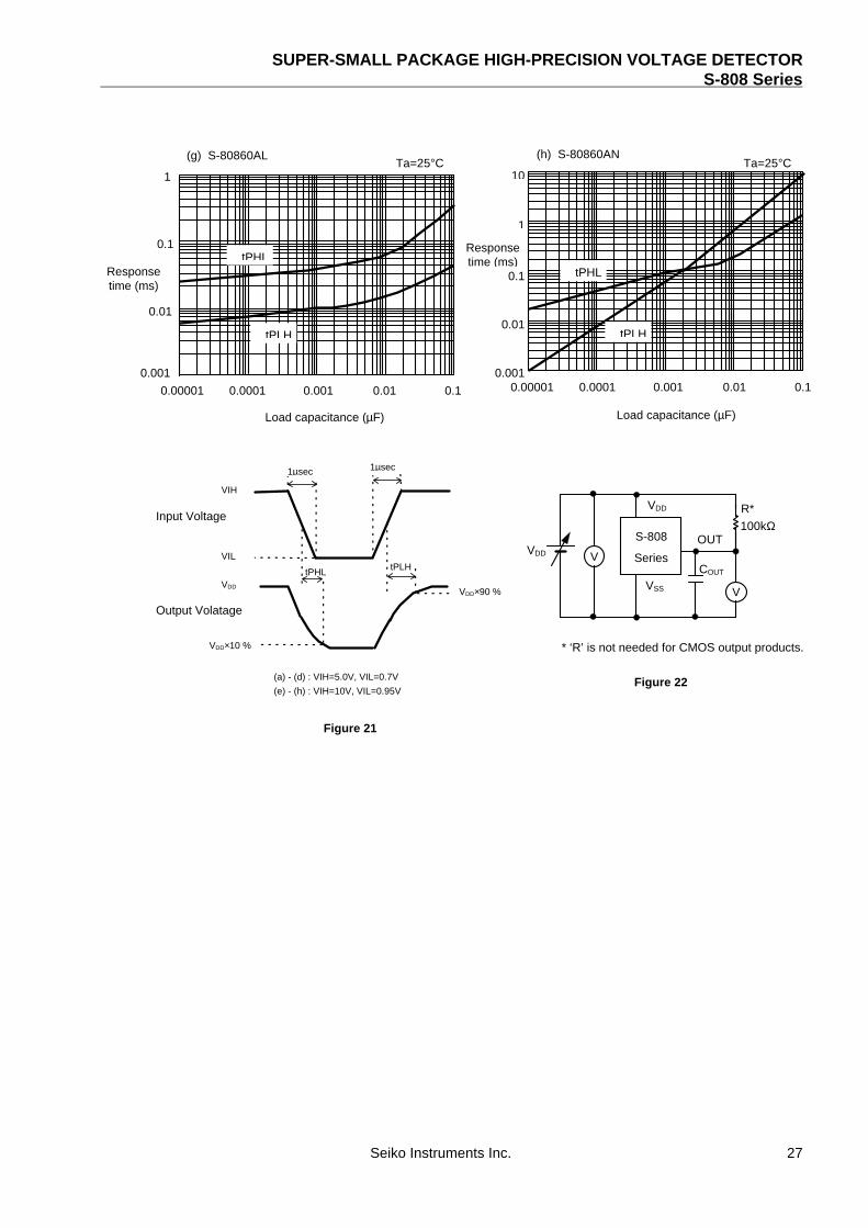
Test Circuits
(1) (2)
R*
100kΩ
V
S-808
Series
OUT
VDD
VSS
VVDD
S-808
Series
OUT
VDD
VSS
A
VDD
* R is unnecessary for CMOS output products.
(3) (4)
A
V
S-808
Series
OUT
VDD
VSS
V
VDS
VDD A
V
S-808
SeriesOUT
VDD
VSS
V
VDS
VDD
Figure 4

SUPER-SMALL PACKAGE HIGH-PRECISION VOLTAGE DETECTORS-808 Series
12 Seiko Instruments Inc.
Technical Terms
1. Detection voltage (-VDET)
The detection voltage -VDET is the voltage at which the output switches to low. This detection voltage varies slightly among
products of the same type. The variation of voltages between the specified minimum [(-VDET)min.] and maximum [(-
VDET)max.] values is called the detection voltage range (See Figure 5).
Example : For the S-80808AN, detection voltage lies in the range of 0.784 ≤ (-VDET) ≤ 0.816.
This means that -VDET is 0.784 in a product while -VDET is 0.816 in another of the same S-80808AN.
2. Release voltage (+VDET)
The release voltage +VDET is the voltage at which the output returns (is “ released” ) to high. This release voltage varies
slightly among products of the same type. The variation of voltages between the specified minimum [(+VDET)min.] and
maximum [(+VDET)max.] values is called the release voltage range (See Figure 6).
Example : For the S-80808AN, the release voltage lies in the range of 0.802 ≤ (+VDET) ≤ 0.867. This means that
+VDET is 0.802 in a product while +VDET is 0.867 in another of the same S-80808AN.
Remark: Although the detection voltage and release voltage overlap in the range of 0.802 V to 0.816 V, +VDET will
always be larger than -VDET.
3. Hysteresis width (VHYS)
The hysteresis width is the voltage difference between the detection voltage and the release voltage
(B-A=VHYS in Figure 10). By giving a device hysteresis, trouble such as noise at the input is avoided.
4. Through-type current
Through-type current refers to the current which flows instantaneously at the time of detection and release of a voltage
detector. Through-type current is large in CMOS output devices, and also flows to some extent in Nch open-drain output
devices.
VD
OUT
(-VDET)Max.
(-VDET)Min.Voltage range Detection
Detection voltage
Figure 5
(+VDET)Max.
(+VDET)MinRelease voltage range
VDRelease voltage
OUT
Figure 6
SUPER-SMALL PACKAGE HIGH-PRECISION VOLTAGE DETECTOR S-808 Series
Seiko Instruments Inc. 13
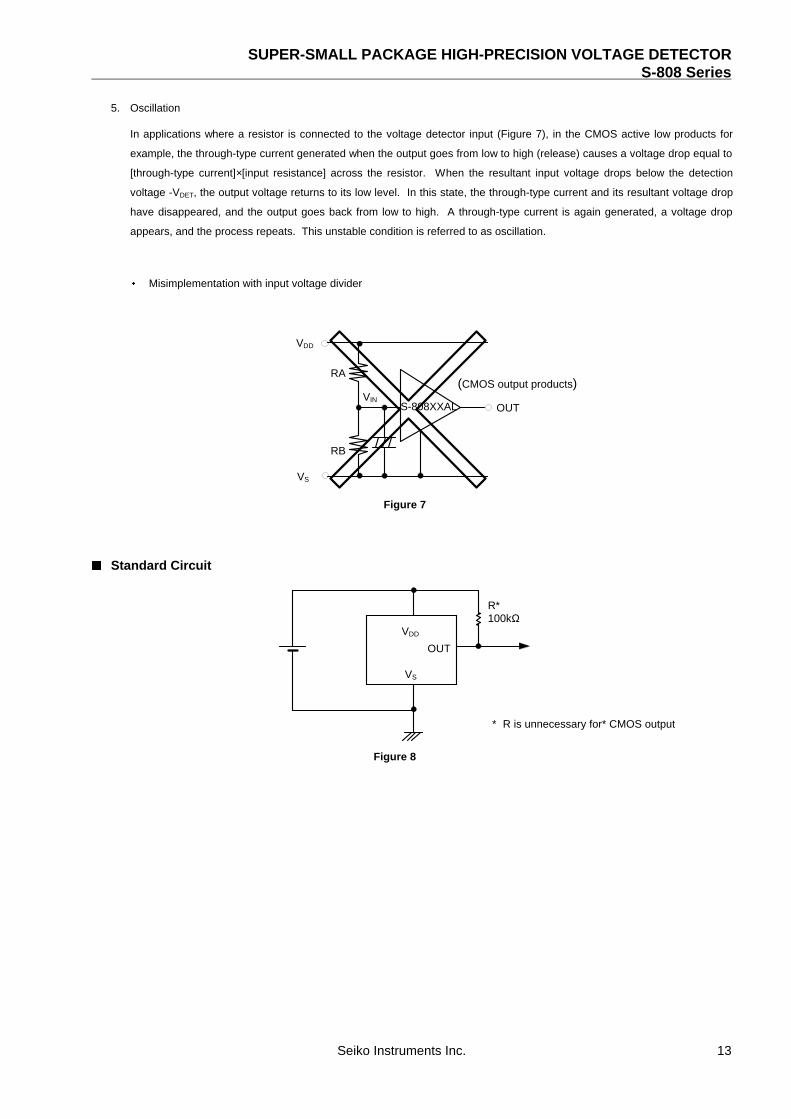
5. Oscillation
In applications where a resistor is connected to the voltage detector input (Figure 7), in the CMOS active low products for
example, the through-type current generated when the output goes from low to high (release) causes a voltage drop equal to
[through-type current]×[input resistance] across the resistor. When the resultant input voltage drops below the detection
voltage -VDET, the output voltage returns to its low level. In this state, the through-type current and its resultant voltage drop
have disappeared, and the output goes back from low to high. A through-type current is again generated, a voltage drop
appears, and the process repeats. This unstable condition is referred to as oscillation.
Misimplementation with input voltage divider
Standard Circuit
RB
RA
OUTVIN
VS
VDD
S-808XXAL
(CMOS output products)
Figure 7
VDD
OUT
VS
R*100kΩ
* R is unnecessary for* CMOS output
Figure 8

SUPER-SMALL PACKAGE HIGH-PRECISION VOLTAGE DETECTORS-808 Series
14 Seiko Instruments Inc.
Operation
1. Basic operation : CMOS active low output
(1) When power supply voltage VDD is greater than the release voltage +VDET, the Nch transistor is OFF and the Pch
transistor ON, causing VDD (high) to appear at the output. With the Nch transistor N1 of Figure 9 OFF, the comparator
input voltage is (RB+RC)/(RA+RB+RC)×VDD.
(2) When power supply voltage VDD goes below +VDET, the output maintains the power supply voltage level, as long as VDD
remains above the detection voltage -VDET. When VDD does fall below -VDET (A in Figure 10), the Nch transistor goes ON,
the Pch transistor goes OFF, and VSS appears at the output. With the Nch transistor N 1 of Figure 9 ON, the comparator
input voltage is RB/(RA+RB) ×VDD.
(3) When VDD falls below the minimum operating voltage, the output becomes undefined. However, output will revert to VDD
if a pull-up has been employed.
(4) VSS will again be output when VDD rises above the minimum operating voltage. VSS will continue to be output even when
VDD surpasses -VDET, as long as it does not exceed the release voltage +VDET.
(5) When VDD rises above +VDET (B in Figure 10), the Nch transistor goes OFF, the Pch transistor goes ON, and VDD
appears at the output.
AB
VD
VSS
Release voltage (+VDET)
Detection voltage (-VDET)
Min. operating voltage
OUT terminal output
Hysteresiswidth (VHYS)
VD
VSS
(1) (2) (3) (5)(4)
+
VREF
RA
−
R
RCN1
VS
VDD
Figure 9
*
OUT
*
Pch
Nch
Figure 10
* Parasitic diode
SUPER-SMALL PACKAGE HIGH-PRECISION VOLTAGE DETECTOR S-808 Series
Seiko Instruments Inc. 15
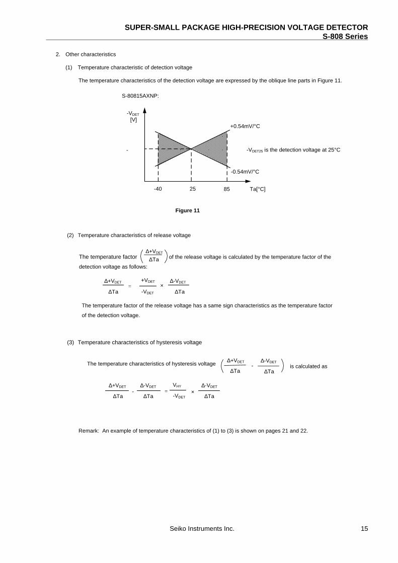
2. Other characteristics
(1) Temperature characteristic of detection voltage
The temperature characteristics of the detection voltage are expressed by the oblique line parts in Figure 11.
(2) Temperature characteristics of release voltage
(3) Temperature characteristics of hysteresis voltage
Remark: An example of temperature characteristics of (1) to (3) is shown on pages 21 and 22.
The temperature factor of the release voltage is calculated by the temperature factor of the
detection voltage as follows:
The temperature characteristics of hysteresis voltage is calculated as
∆+VDET
∆Ta-
∆-VDET
∆Ta=
VHY
-VDET×
∆-VDET
∆Ta
∆+VDET
∆Ta-
∆-VDET
∆Ta
-40 25
+0.54mV/°C
-VDET
[V]
-VDET25 is the detection voltage at 25°C-
85 Ta[°C]
-0.54mV/°C
Figure 11
S-80815AXNP:
The temperature factor of the release voltage has a same sign characteristics as the temperature factor
of the detection voltage.
∆Ta
∆-VDET×
+VDET
-VDET
=∆+VDET
∆Ta
∆Ta
∆+VDET
SUPER-SMALL PACKAGE HIGH-PRECISION VOLTAGE DETECTORS-808 Series
16 Seiko Instruments Inc.
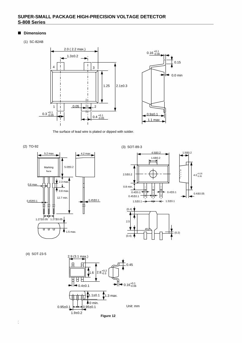
Dimensions
(1) SC-82AB
(2) TO-92
Figure 12
0.8 min.
2.5±0.2 4.0
1.5±0.2
0.4±0.05
1.5±0.1
0.4±0.10.4±0.1
4.5±0.2
1.6±0.2
0.45±0.1
Unit: mm
(3) SOT-89-3
2.5
45°
(0.4)(0.2)
+0.25-0.35
(0.4)
0.45±0.112.7 min.
1.5 max.
4.2 max.
0.8 max.
0.45±0.1
0.6 max.
5.2 max.
Marking
face
0.9±0.1
1.1 max
2
0.3 +0.1-0.05
0.4 +0.1-0.05
2.0 ( 2.2 max.)
1.25 2.1±0.3
1.3±0.2
1
34
5.0±0.2
2.3 max.
1.27±0.05 1.27±0.05
0.95±0.1
2.8
0.4±0.1
0.0 min
0 min.
0.15
1.1±0.1 1.3 max.
0.16 +0.1-0.06
1.6
2.9 (3.1 max.)
0.05
+0.2-0.3
0.95±0.1
1.9±0.2
0.16+0.1-0.06
0.45
(4) SOT-23-5
1.5±0.1
The surface of lead wire is plated or dipped with solder.
SUPER-SMALL PACKAGE HIGH-PRECISION VOLTAGE DETECTOR S-808 Series
Seiko Instruments Inc. 17
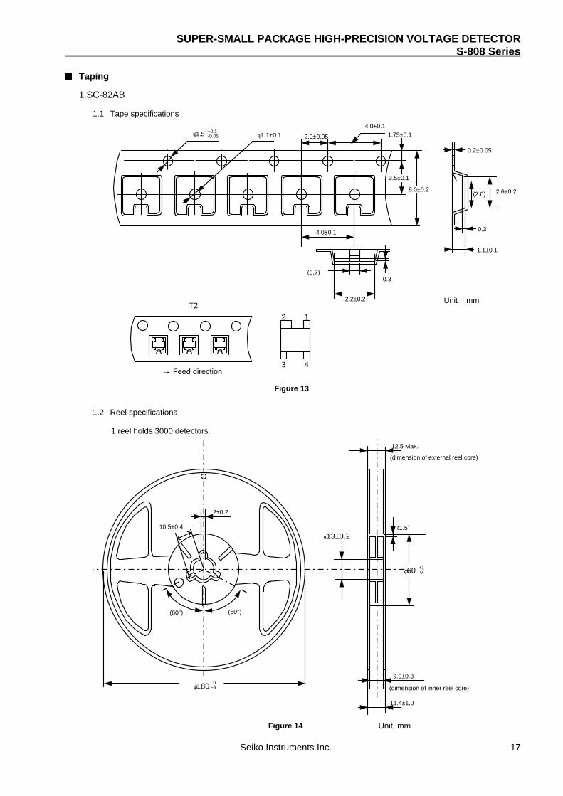
Taping
1.SC-82AB
1.1 Tape specifications
1.2 Reel specifications
1 reel holds 3000 detectors.
Figure 14
(2.0)
0.3
1.1±0.1
2.6±0.2
(0.7)
T2
0.2±0.05
4.0±0.1
φ1.1±0.1φ1.5 +0.1-0.05 2.0±0.05
4.0±0.1
3.5±0.1
8.0±0.2
0.3
2.2±0.2
2 1
43
1.75±0.1
→ Feed direction
Unit : mm
Figure 13
φ180 0−3
12.5 Max.
φ60 +1 0
(dimension of external reel core)
(1.5)
9.0±0.3
(dimension of inner reel core)
11.4±1.0
10.5±0.4
φ13±0.2
(60°)(60°)
2±0.2
Unit: mm
SUPER-SMALL PACKAGE HIGH-PRECISION VOLTAGE DETECTORS-808 Series
18 Seiko Instruments Inc.
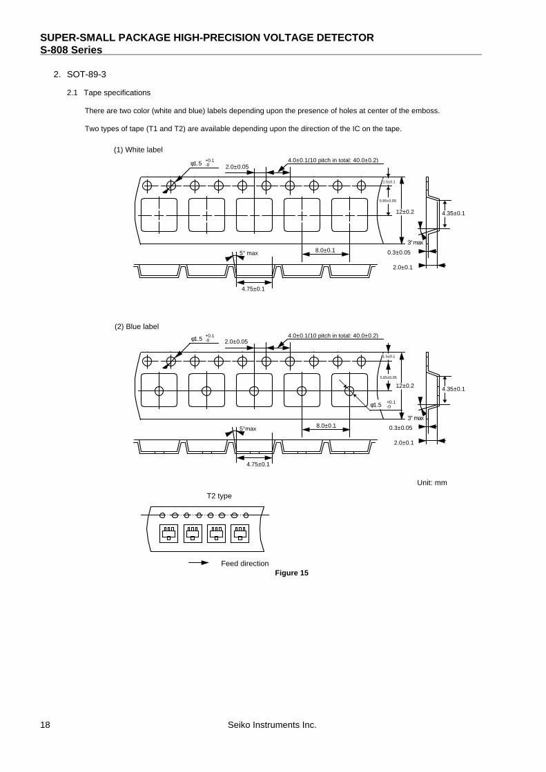
2. SOT-89-3
2.1 Tape specifications
There are two color (white and blue) labels depending upon the presence of holes at center of the emboss.
Two types of tape (T1 and T2) are available depending upon the direction of the IC on the tape.
Unit: mm
T2 type
Feed direction
(1) White label
(2) Blue label
3° max
2.0±0.05φ1.5 4.0±0.1(10 pitch in total: 40.0±0.2)
4.75±0.1
8.0±0.1
+0.1-0
0.3±0.05
2.0±0.1
5° max
3° max
2.0±0.05φ1.5 4.0±0.1(10 pitch in total: 40.0±0.2)
4.75±0.1
8.0±0.1
+0.1-0
0.3±0.05
2.0±0.1
5°max
1.5±0.1
5.65±0.05
12±0.2
4.35±0.1
1.5±0.1
5.65±0.05
12±0.2
4.35±0.1
Figure 15
φ1.5 +0.1-0

SUPER-SMALL PACKAGE HIGH-PRECISION VOLTAGE DETECTOR S-808 Series
Seiko Instruments Inc. 19
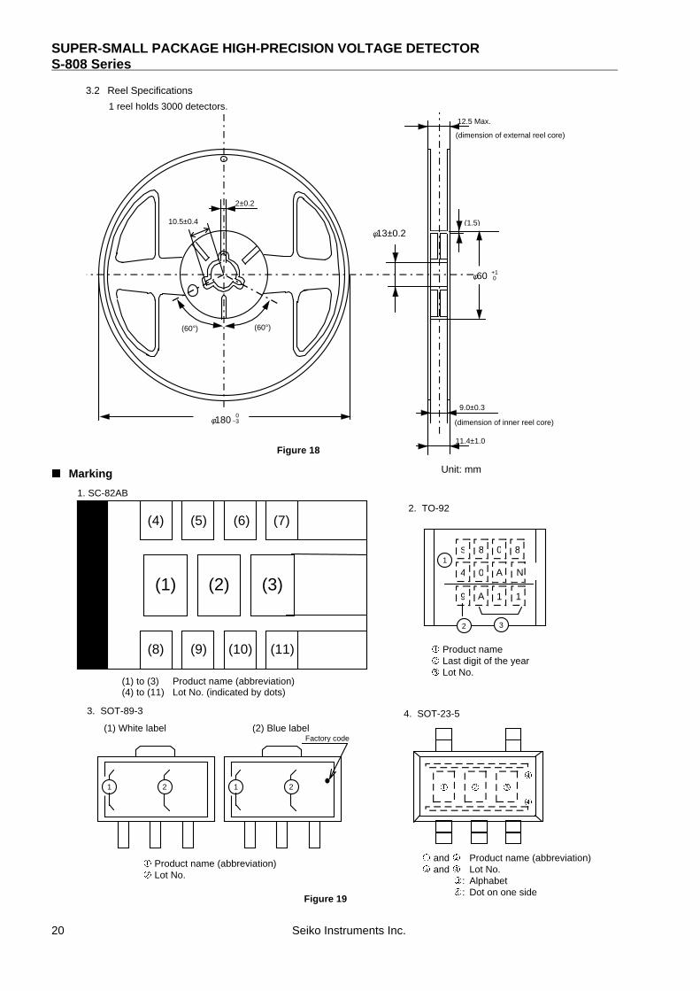
2.2 Reel specifications
1 reel holds 1000 detectors.
3. SOT-23-5
3.1 Tape specifications
The emboss cover tape comes in two tones (milk white/transparent and transparent).
3°max
3.2±0.1
0.27±0.05
1.4±0.1
3° max
φ180 0-3
16.5 Max.
(1.5)
13.0±0.3
10.5±0.4
φ13±0.2
(60°)(60°)
2±0.2
Unit: mm
4.0±0.1
φ1.0φ1.5+0.1-0
+0.2-0 2.0±0.05 4.0±0.1(10 pitchin total: 40.0±0.2)
1.75±0.1
3.5±0.05
8.0±0.2
Unit: mm
T2 type
→ Feed direction
3.23±0.1
Figure 17
Figure 16
φ60.0 +1 -0
15.4±1.0
SUPER-SMALL PACKAGE HIGH-PRECISION VOLTAGE DETECTORS-808 Series
20 Seiko Instruments Inc.
3.2 Reel Specifications
1 reel holds 3000 detectors.
Marking
Figure 18
φ180 0−3
12.5 Max.
φ60 +1 0
(dimension of external reel core)
(1.5)
9.0±0.3
(dimension of inner reel core)
11.4±1.0
10.5±0.4
φ13±0.2
(60°)(60°)
2±0.2
Unit: mm
S
(1) to (3) Product name (abbreviation)(4) to (11) Lot No. (indicated by dots)
1. SC-82AB
Figure 19
(3)
(4) (7)
(8) (9) (10) (11)
(2)(1)
(6)(5)
Product name Last digit of the year Lot No.
2. TO-92
32
18 80
0
9 1
4 A N
1A
3. SOT-89-3
(1) White label (2) Blue label
1
Product name (abbreviation) Lot No.
2 1 2
Factory code
and Product name (abbreviation) and Lot No.
: Alphabet: Dot on one side
4. SOT-23-5

SUPER-SMALL PACKAGE HIGH-PRECISION VOLTAGE DETECTOR S-808 Series
Seiko Instruments Inc. 21
Characteristics (typical characteristics)
(1) Detection voltage (VDET) - Temperature (Ta)
10 40
Ta (°C)
3020-10
VDET
(V)
(a) S-80808AL (b) S-80814AL
1.3
1.35
1.4
1.45
1.5
1.55
1.6
VDET
(V)
Ta (°C)
0.76
0.74
0.78
0.8
0.82
0.84
0.86
0.88
0.9
-20 706050
+VDET
-VDET -VDET
+VDET
20 80
Ta (°C)
60400-20
VDET
(V)
(c) S-80815AL(d) S-80860AL
5.95
6.00
6.05
6.15
VDET
(V)
1.45
1.50
1.55
1.60
-40
20 8060400-20-40
6.10
6.20
6.25
-VDET
+VDET
0
+VDET
-VDET
10 403020-10-20 7060500
Ta (°C)
SUPER-SMALL PACKAGE HIGH-PRECISION VOLTAGE DETECTORS-808 Series
22 Seiko Instruments Inc.
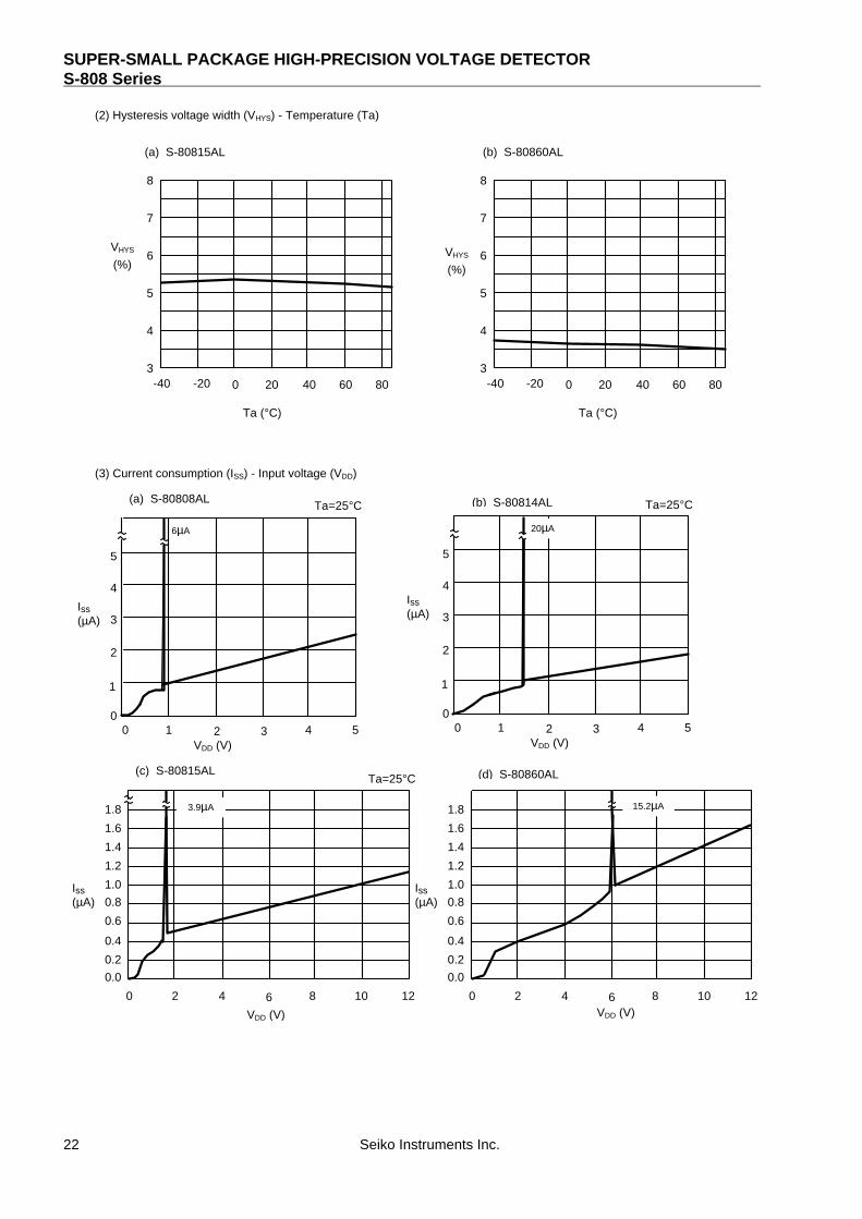
(2) Hysteresis voltage width (VHYS) - Temperature (Ta)
(3) Current consumption (ISS) - Input voltage (VDD)
Iss(µA)
(a) S-80808AL
VDD (V)
(b) S-80814AL
0 1 2 3 4 50
1
2
3
4
5
Iss(µA)
Ta (°C)
VDD (V)
(a) S-80815AL (b) S-80860AL
20 8060400
0
-20
1 2 3 4 50
1
-40
2
3
4
8
5
7
6
5
4
3
VHYS
(%)
Ta (°C)
6µA
20
20µA
8060400-20-40
8
7
6
5
4
3
VHYS
(%)
Ta=25°C Ta=25°C
Ta=25°C
Iss(µA)
(c) S-80815AL
VDD (V)
(d) S-80860AL
0 2 4 6 8 12
1.8
VDD (V)
3.9µA
10
1.6
1.4
1.2
1.0
0.8
0.6
0.4
0.2
0.0
Iss(µA)
0 2 4 6 8 12
1.8 15.2µA
10
1.6
1.4
1.2
1.0
0.8
0.6
0.4
0.2
0.0
SUPER-SMALL PACKAGE HIGH-PRECISION VOLTAGE DETECTOR S-808 Series
Seiko Instruments Inc. 23
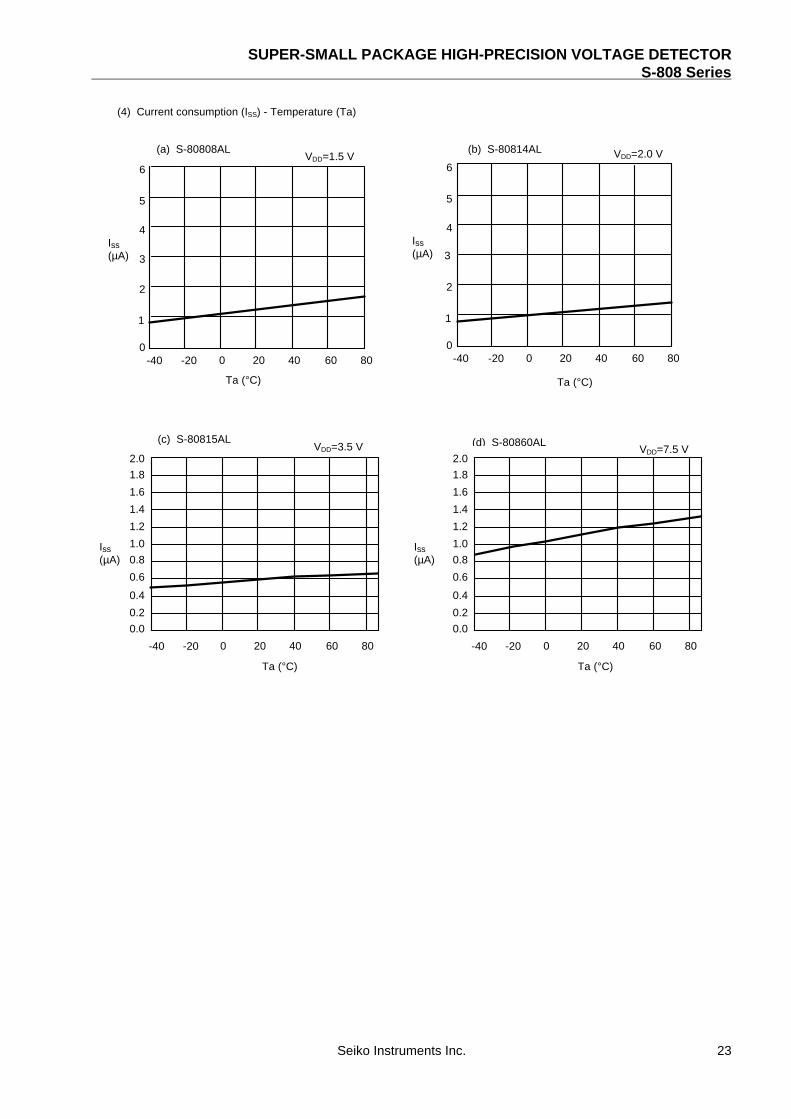
(4) Current consumption (ISS) - Temperature (Ta)
806040200-20-40 806040200-20-40
VDD=1.5 V(a) S-80808AL
Iss(µA)
0
1
2
3
4
5
6VDD=2.0 V(b) S-80814AL
Iss(µA)
0
1
2
3
4
5
6
Ta (°C)Ta (°C)
VDD=3.5 V
Iss(µA)
(c) S-80815AL (d) S-80860AL
1.8
1.6
1.4
1.2
1.0
0.8
0.6
0.4
0.2
0.0
Iss(µA)
2.0
Ta (°C) Ta (°C)
806040200-20-40
1.8
1.6
1.4
1.2
1.0
0.8
0.6
0.4
0.2
0.0
2.0
806040200-20-40
VDD=7.5 V
SUPER-SMALL PACKAGE HIGH-PRECISION VOLTAGE DETECTORS-808 Series
24 Seiko Instruments Inc.
(5) Nch transistor output current (IOUT) - VDS
(6) Pch transistor output current (IOUT) - VDS
(7) Nch transistor output current (IOUT) - Input voltage(VDD)
Ta=25°CTa=25°C
Ta=25°C
VDS (V)
(a) S-80814AL (b) S-80860AL
IOUT
(mA)
VDS (V)
0 0.5 1 20
0.5
1
1.5
2.5
1.5
2 VDD=1.3 V
VDD=1.0 V
VDD=0.7 V
60
50
40
30
20
10
00 1 2 3 4 5
VDD=6.0 V
VDD=4.8 V
VDD=3.6 V
VDD=2.4 V
VDD=1.2V
IOUT
(mA)
(a) S-80808AL
IOUT
(mA)
VDS (V)
0
32.521.50.50 1
1
2
3
4
5
VDD=0.9 V
VDD=1.4 V
VDD=1.9 V
VDD=2.4 V
VDD=2.9 V
(b) S-80815AL
VDS (V)
30
25
20
15
10
5
00 2 4 6 8 10
IOUT
(mA)
VDD=8.4 V
VDD=7.2 V
VDD=6.0 V
VDD=4.8 V
VDD=3.6 V
VDD=2.4 V
VDS =0.5VVDS =0.5V(a) S -80814AL
VDD (V)
(b) S-80860AL
00
0.5
1
2
3
0.5 1 21.5
2.5
1.5
IOUT
(mA)
Ta=-30°C
Ta=25°C
Ta=80°C
20
15
10
5
00 2 4 6 8
IOUT
(mA)
Ta=-40°C
Ta=-25°C
Ta=85°C
VDD (V)
SUPER-SMALL PACKAGE HIGH-PRECISION VOLTAGE DETECTOR S-808 Series
Seiko Instruments Inc. 25
(8) Pch transistor output current(IOUT) - Input voltage(VDD)
(9) Minimum operating voltage
VDS =0.5V
Ta=80°C
Ta=25°C
Ta=-30°C
(a) S-80814AL
VDD (V)
0 1.5 2 2.5 30
0.5
1
2
3
2.5
1.5
IOUT
(mA)
VDS =0.5V
5.0
4.0
3.0
2.0
1.0
00 2 4 6 8 10 12
Ta=-40°CTa=25°C
Ta=85°C
(b) S-80815AL
VOUT
(V)1.0
(c) S-80815AN
(PULL- UP VDD : 100KΩ)
(d) S-80815AN
(PULL- UP VDD : 100KΩ)
PULL UP (V)
0.0
0.
VDD (V)
0.5
1.5
0.5 1.0 1.5 2.0
2.0
Ta=-40°C
Ta =25°C
Ta=80°C
VDDMIN
(V)
0.75
0.70
0.65
0.60
0.55
0.503.0 6.0 9.0 12.0
Notice
VOUT
(V)
PULL UP
PULL UP×0.10 VDD (V)VDDMIN
Ta=-40°C
Ta =25°C
0.4
Ta=85°C
Ta =25°CVOUT
(mA)
0.6
(a) S-80808AN(PULL- UP 3.0 V : 100K)
(b) S-80808AL
VOUT
(mA)
0
1
2
3
4
0.60.40.20
(PULL- UP VDD : 100K)
0.8 1
VDD (V)
0
0.2
0.60.20 0.8 1
VDD (V)
0.4
0.8
1
Ta =25°CTa=80°C
Ta=80°C
Ta=-30°C
Ta=-30°C
VDD (V)
IOUT
(mA)
Figure 20
Remark:
VDDMIN is defined with VDD when VOUT goes
below 10% of the PULL UP voltage as shown
in Figure 20 when raising VDD from 0 V.
SUPER-SMALL PACKAGE HIGH-PRECISION VOLTAGE DETECTORS-808 Series
26 Seiko Instruments Inc.
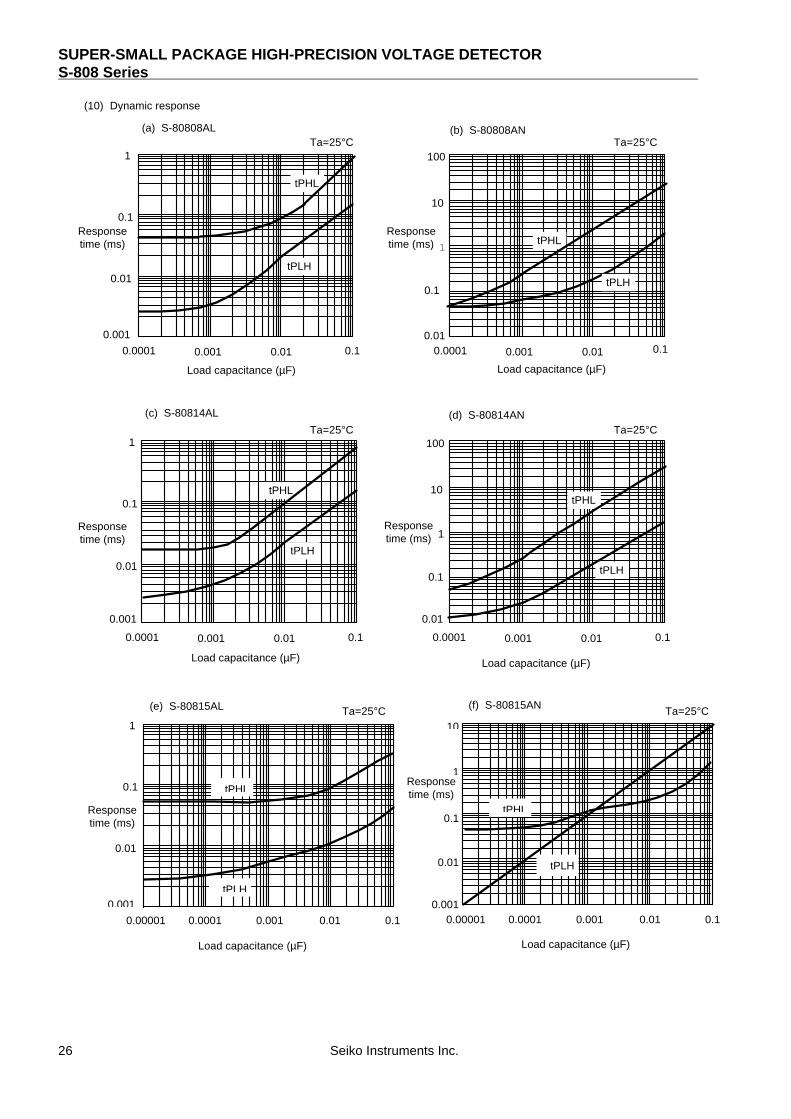
(10) Dynamic response
(e) S-80815AL
Responsetime (ms)
(a) S-80808AL (b) S-80808AN
1
(f) S-80815AN
0.1
(d) S-80814AN
0.01
0.1
1
10
100
0.0001 0.001 0.01 0.1
(c) S-80814AL
0.0001 0.001 0.01 0.1
0.001
1
0.01
0.1
tPLH
tPHL
tPLH
tPHL
Load capacitance (µF) Load capacitance (µF)
Load capacitance (µF)
Load capacitance (µF)
Responsetime (ms)
Responsetime (ms)
Responsetime (ms)
Responsetime (ms)
Load capacitance (µF)
Load capacitance (µF)
Responsetime (ms)
0.01
0.1
1
10
100
0.0001 0.001 0.01 0.1
0.001
0.01
0.1
0.0001 0.001 0.01
tPLH
tPHL
tPLH
tPHL
0.001
1
0.01
0.1
0.00001 0.0001 0.001 0.01 0.1
Ta=25°C
Ta=25°C
Ta=25°C
Ta=25°C
Ta=25°C Ta=25°C
0.1
1
10
0.01
0.0010.00001 0.0001 0.001 0.01 0.1
tPHL
tPLH
tPHL
tPLH
SUPER-SMALL PACKAGE HIGH-PRECISION VOLTAGE DETECTOR S-808 Series
Seiko Instruments Inc. 27
(g) S-80860AL
Load capacitance (µF)
(h) S-80860AN
Load capacitance (µF)
0.001
1
0.01
0.1
0.00001 0.0001 0.001 0.01 0.1 0.1
0.1
1
10
0.01
0.0010.00001 0.0001 0.001 0.01
tPHL
tPLH
tPHL
tPLH
Responsetime (ms)
Responsetime (ms)
COUT
VDD
VSS
OUT
VDD
V
S-808
Series
V
R*
* ‘R’ is not needed for CMOS output products.
100kΩ
VDD×90 %
VDD×10 %
VIH
VIL
VDD
tPHL tPLH
(a) - (d) : VIH=5.0V, VIL=0.7V
(e) - (h) : VIH=10V, VIL=0.95V
1µsec1µsec
Input Voltage
Output Volatage
Figure 21
Figure 22
Ta=25°C Ta=25°C
SUPER-SMALL PACKAGE HIGH-PRECISION VOLTAGE DETECTORS-808 Series
28 Seiko Instruments Inc.
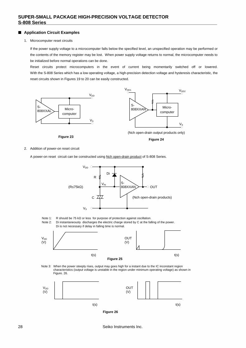
Application Circuit Examples
1. Microcomputer reset circuits
If the power supply voltage to a microcomputer falls below the specified level, an unspecified operation may be performed or
the contents of the memory register may be lost. When power supply voltage returns to normal, the microcomputer needs to
be initialized before normal operations can be done.
Reset circuits protect microcomputers in the event of current being momentarily switched off or lowered.
With the S-808 Series which has a low operating voltage, a high-precision detection voltage and hysteresis characteristic, the
reset circuits shown in Figures 19 to 20 can be easily constructed.
2. Addition of power-on reset circuit
A power-on reset circuit can be constructed using Nch open-drain product of S-808 Series.
(Nch open-drain products)
OUTVIN
VS
VDD
Note 1: R should be 75 kΩ or less for purpose of protection against oscillation.Note 2: Di instantaneously discharges the electric charge stored by C at the falling of the power.
Di is not necessary if delay in falling time is normal.
S-808XXAN
R
C
Di
(R≤75kΩ)
VDD
(V)
t(s)
OUT(V)
t(s)Figure 25
Note 3: When the power steeply rises, output may goes high for a instant due to the IC inconstant regioncharacteristics (output voltage is unstable in the region under minimum operating voltage) as shown inFigure. 26.
VDD
(V)
t(s)
OUT(V)
t(s)
Figure 26
VS
VS
VDD
Micro-computer
S-808XXAL
Figure 23(Nch open-drain output products only)
VDD1 VDD2
Micro-computer
S-808XXAN
Figure 24
SUPER-SMALL PACKAGE HIGH-PRECISION VOLTAGE DETECTOR S-808 Series
Seiko Instruments Inc. 29
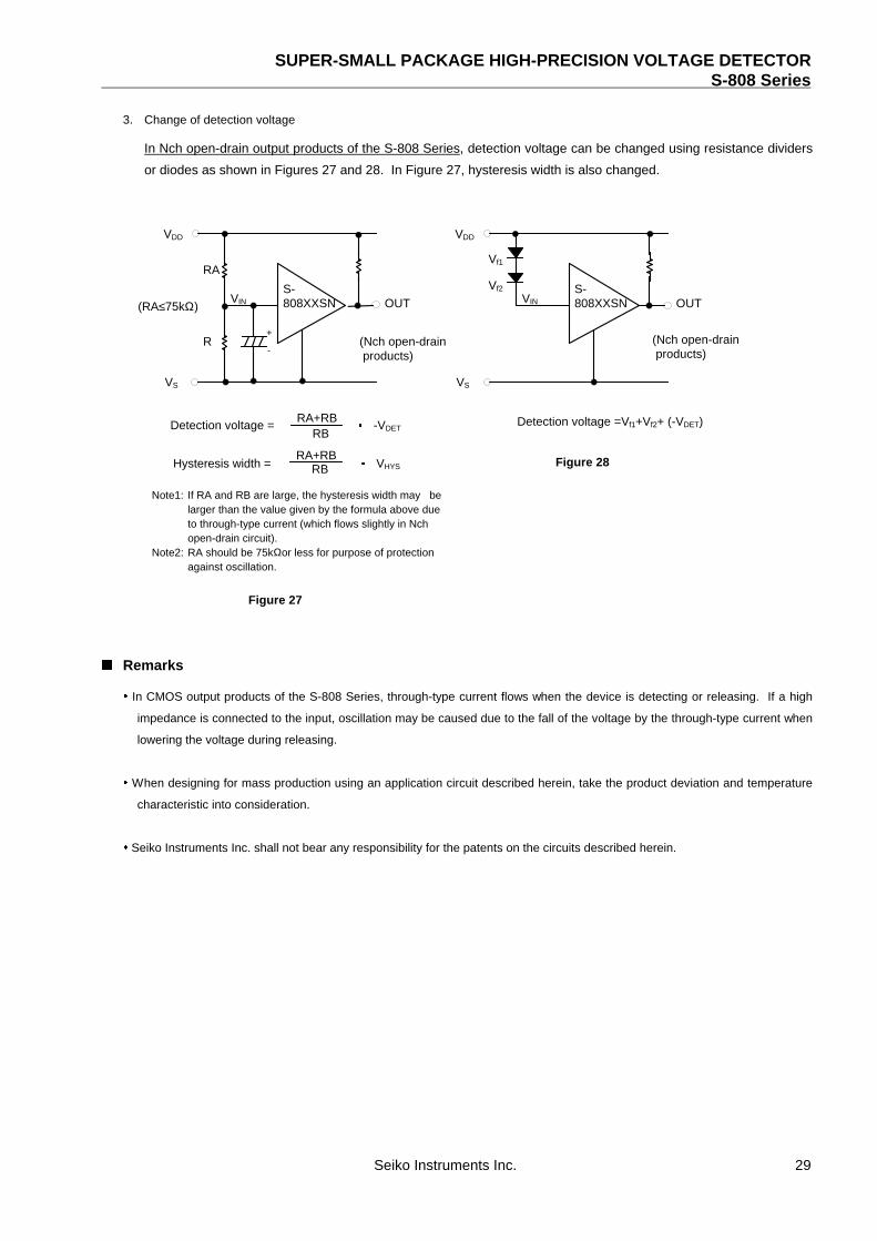
3. Change of detection voltage
In Nch open-drain output products of the S-808 Series, detection voltage can be changed using resistance dividers
or diodes as shown in Figures 27 and 28. In Figure 27, hysteresis width is also changed.
Remarks
In CMOS output products of the S-808 Series, through-type current flows when the device is detecting or releasing. If a high
impedance is connected to the input, oscillation may be caused due to the fall of the voltage by the through-type current when
lowering the voltage during releasing.
When designing for mass production using an application circuit described herein, take the product deviation and temperature
characteristic into consideration.
Seiko Instruments Inc. shall not bear any responsibility for the patents on the circuits described herein.
(Nch open-drain products)
RA
OUTVIN
VS
VDD
Note1: If RA and RB are large, the hysteresis width may belarger than the value given by the formula above dueto through-type current (which flows slightly in Nchopen-drain circuit).
Note2: RA should be 75kΩor less for purpose of protectionagainst oscillation.
+
-
S-808XXSN
Figure 27
R (Nch open-drain products)
Vf1
OUTVIN
VS
VDD
S-808XXSN
Vf2
Detection voltage = -VDETRA+RB
RB
Hysteresis width = VHYSRA+RB
RBFigure 28
Detection voltage =Vf1+Vf2+ (-VDET)
(RA≤75kΩ)
30
Collection of Product FAQs
Author: Imura Yukihiro Date : 99/05/27 (Thurday) 13:43 (Modified: 99/05/28 (Friday) 09:55)
<Information level>
A: Public (Printing O.K.)
Index: A: General
<Product>
Division name: 01 IC
Category 1: 11 Power Supply
Category 2: 1. Voltage Detectors
Cal No.: S-808
Related Documents:
Question:
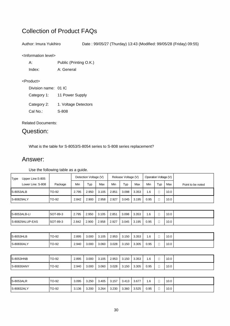
What is the table for S-8053/S-8054 series to S-808 series replacement?
Answer:
Use the following table as a guide.
Type Upper Line:S-805 Detection Voltage (V) Release Voltage (V) Operation Voltage (V)
Lower Line: S-808 Package Min Typ Max Min Typ Max Min Typ Max Point to be noted
S-8053ALB TO-92 2.795 2.950 3.105 2.851 3.098 3.353 1.6 10.0
S-80829ALY TO-92 2.842 2.900 2.958 2.927 3.045 3.195 0.95 10.0
S-8053ALB-LI SOT-89-3 2.795 2.950 3.105 2.851 3.098 3.353 1.6 10.0
S-80829ALUP-EAS SOT-89-3 2.842 2.900 2.958 2.927 3.045 3.195 0.95 10.0
S-8053HLB TO-92 2.895 3.000 3.105 2.953 3.150 3.353 1.6 10.0
S-80830ALY TO-92 2.940 3.000 3.060 3.028 3.150 3.305 0.95 10.0
S-8053HNB TO-92 2.895 3.000 3.105 2.953 3.150 3.353 1.6 10.0
S-80830ANY TO-92 2.940 3.000 3.060 3.028 3.150 3.305 0.95 10.0
S-8053ALR TO-92 3.095 3.250 3.405 3.157 3.413 3.677 1.6 10.0
S-80832ALY TO-92 3.136 3.200 3.264 3.230 3.360 3.525 0.95 10.0

31
S-8053ALR-LJ SOT-89-3 3.095 3.250 3.405 3.157 3.413 3.677 1.6 10.0
S-80832ALUP-EAW SOT-89-3 3.136 3.200 3.264 3.230 3.360 3.525 0.95 10.0
S-8053ANO TO-92 3.395 3.550 3.705 3.463 3.728 4.001 1.6 10.0
S-80835ANY TO-92 3.430 3.500 3.570 3.533 3.675 3.856 0.95 10.0
S-8054ALB TO-92 3.995 4.150 4.305 4.075 4.358 4.649 1.6 10.0
S-80841ALY TO-92 4.018 4.100 4.182 4.139 4.305 4.517 0.95 10.0
S-8054ALB-LM SOT-89-3 3.995 4.150 4.305 4.075 4.358 4.649 1.6 10.0
S-80841ALUP-EA5 SOT-89-3 4.018 4.100 4.182 4.139 4.305 4.517 0.95 10.0
S-8054ALR TO-92 4.295 4.450 4.605 4.381 4.673 4.973 1.6 10.0
S-80844ALY TO-92 4.312 4.400 4.488 4.441 4.620 4.847 0.95 10.0
S-8054ALR-LN SOT-89-3 4.295 4.450 4.605 4.381 4.673 4.973 1.6 10.0
S-80844ALUP-EA8 SOT-89-3 4.312 4.400 4.488 4.441 4.620 4.847 0.95 10.0
S-8054ALO TO-92 4.595 4.750 4.905 4.687 4.988 5.297 1.6 10.0
S-80847ALY TO-92 4.606 4.700 4.794 4.744 4.935 5.178 0.95 10.0
S-8054ALO-LO SOT-89-3 4.595 4.750 4.905 4.687 4.988 5.297 1.6 10.0
S-80847ALUP-EEB SOT-89-3 4.606 4.700 4.794 4.744 4.935 5.178 0.95 10.0
S-8054ALY TO-92 4.895 5.100 5.205 4.993 5.355 5.621 1.6 10.0
S-80851ALY TO-92 4.998 5.100 5.202 5.148 5.355 5.618 0.95 10.0
S-8054ALY-LP SOT-89-3 4.895 5.100 5.205 4.993 5.355 5.621 1.6 10.0
S-80851ALUP-EEF SOT-89-3 4.998 5.100 5.202 5.148 5.355 5.618 0.95 10.0
S-8054HN TO-92 3.800 4.000 4.200 3.876 4.200 4.536 1.6 10.0
S-80839ANY TO-92 3.822 3.900 3.978 3.937 4.095 4.296 0.95 10.0
S-8054HN-CB SOT-89-3 3.800 4.000 4.200 3.876 4.200 4.536 1.6 10.0
S-80839ANUP-ED3 SOT-89-3 3.822 3.900 3.978 3.937 4.095 4.296 0.95 10.0
32
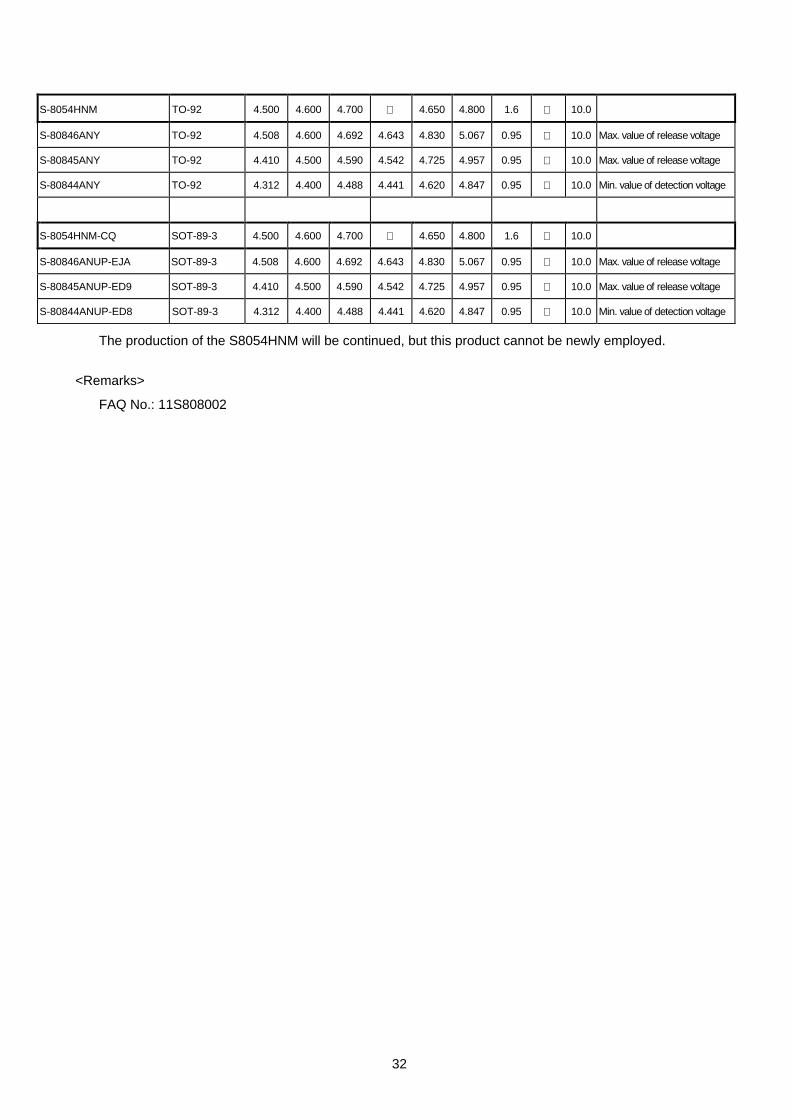
S-8054HNM TO-92 4.500 4.600 4.700 4.650 4.800 1.6 10.0
S-80846ANY TO-92 4.508 4.600 4.692 4.643 4.830 5.067 0.95 10.0 Max. value of release voltage
S-80845ANY TO-92 4.410 4.500 4.590 4.542 4.725 4.957 0.95 10.0 Max. value of release voltage
S-80844ANY TO-92 4.312 4.400 4.488 4.441 4.620 4.847 0.95 10.0 Min. value of detection voltage
S-8054HNM-CQ SOT-89-3 4.500 4.600 4.700 4.650 4.800 1.6 10.0
S-80846ANUP-EJA SOT-89-3 4.508 4.600 4.692 4.643 4.830 5.067 0.95 10.0 Max. value of release voltage
S-80845ANUP-ED9 SOT-89-3 4.410 4.500 4.590 4.542 4.725 4.957 0.95 10.0 Max. value of release voltage
S-80844ANUP-ED8 SOT-89-3 4.312 4.400 4.488 4.441 4.620 4.847 0.95 10.0 Min. value of detection voltage
The production of the S8054HNM will be continued, but this product cannot be newly employed.
<Remarks>
FAQ No.: 11S808002
33
Collection of Product FAQs
Author: Imura Yukihiro Date: 99/05/27 (Thursday) 13:12 (Modified: 99/05/27 (Thursday) 13:37)
<Information level>
A: Public (Printing O.K.)
Index: A: General
<Product>
Division name: 01 IC
Category 1: 11 Power Supply
Category 2: 1. Voltage Detectors
Cal No.: S-808
Related Documents:
Question:
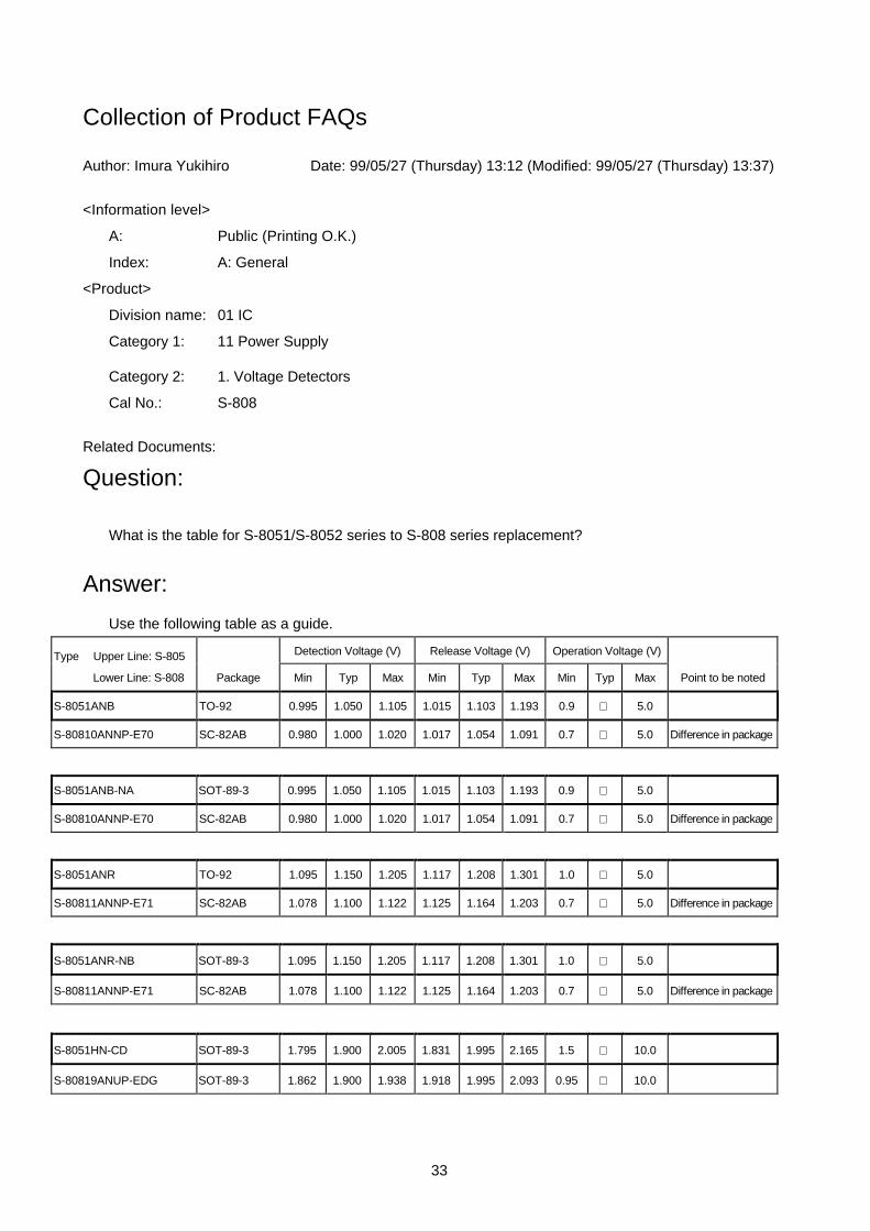
What is the table for S-8051/S-8052 series to S-808 series replacement?
Answer:
Use the following table as a guide.
Type Upper Line: S-805 Detection Voltage (V) Release Voltage (V) Operation Voltage (V)
Lower Line: S-808 Package Min Typ Max Min Typ Max Min Typ Max Point to be noted
S-8051ANB TO-92 0.995 1.050 1.105 1.015 1.103 1.193 0.9 5.0
S-80810ANNP-E70 SC-82AB 0.980 1.000 1.020 1.017 1.054 1.091 0.7 5.0 Difference in package
S-8051ANB-NA SOT-89-3 0.995 1.050 1.105 1.015 1.103 1.193 0.9 5.0
S-80810ANNP-E70 SC-82AB 0.980 1.000 1.020 1.017 1.054 1.091 0.7 5.0 Difference in package
S-8051ANR TO-92 1.095 1.150 1.205 1.117 1.208 1.301 1.0 5.0
S-80811ANNP-E71 SC-82AB 1.078 1.100 1.122 1.125 1.164 1.203 0.7 5.0 Difference in package
S-8051ANR-NB SOT-89-3 1.095 1.150 1.205 1.117 1.208 1.301 1.0 5.0
S-80811ANNP-E71 SC-82AB 1.078 1.100 1.122 1.125 1.164 1.203 0.7 5.0 Difference in package
S-8051HN-CD SOT-89-3 1.795 1.900 2.005 1.831 1.995 2.165 1.5 10.0
S-80819ANUP-EDG SOT-89-3 1.862 1.900 1.938 1.918 1.995 2.093 0.95 10.0

34
S-8052ANB-NE SOT-89-3 1.995 2.100 2.205 2.035 2.205 2.381 1.5 10.0
S-80821ANUP-EDJ SOT-89-3 2.058 2.100 2.142 2.120 2.205 2.313 0.95 10.0
S-8052ALB TO-92 1.995 2.100 2.205 2.035 2.205 2.381 1.5 10.0
S-80821ALY TO-92 2.058 2.100 2.142 2.120 2.205 2.313 0.95 10.0
S-8052ALB-LE SOT-89-3 1.995 2.100 2.205 2.035 2.205 2.381 1.5 10.0
S-80821ALUP-EAJ SOT-89-3 2.058 2.100 2.142 2.120 2.205 2.313 0.95 10.0
S-8052ALR TO-92 2.195 2.300 2.405 2.239 2.415 2.597 1.5 10.0
S-80823ALY TO-92 2.254 2.300 2.346 2.322 2.415 2.534 0.95 10.0
S-8052ALR-LF SOT-89-3 2.195 2.300 2.405 2.239 2.415 2.597 1.5 10.0
S-80823ALUP-EAL SOT-89-3 2.254 2.300 2.346 2.322 2.415 2.534 0.95 10.0
S-8052ALO TO-92 2.395 2.500 2.605 2.443 2.625 2.813 1.5 10.0
S-80825ALY TO-92 2.450 2.500 2.550 2.524 2.625 2.754 0.95 10.0
S-8052ALO-LG SOT-89-3 2.395 2.500 2.605 2.443 2.625 2.813 1.5 10.0
S-80825ALUP-EAN SOT-89-3 2.450 2.500 2.550 2.524 2.625 2.754 0.95 10.0
S-8052ALY TO-92 2.595 2.700 2.805 2.647 2.835 3.029 1.5 10.0
S-80827ALY TO-92 2.646 2.700 2.754 2.725 2.835 2.974 0.95 10.0
S-8052ALY-LH SOT-89-3 2.595 2.700 2.805 2.647 2.835 3.029 1.5 10.0
S-80827ALUP-EAQ SOT-89-3 2.646 2.700 2.754 2.725 2.835 2.974 0.95 10.0
S-8052ANY-NH SOT-89-3 2.595 2.700 2.805 2.647 2.835 3.029 1.5 10.0
S-80827ANUP-EDQ SOT-89-3 2.646 2.700 2.754 2.725 2.835 2.974 0.95 10.0
S-8052HNM TO-92 2.295 2.400 2.505 4.300 4.400 4.500 1.5 10.0
S-80824ANY TO-92 2.352 2.400 2.448 2.423 2.520 2.644 0.95 10.0 Release voltage
S-8052HNM-CR SOT-89-3 2.295 2.400 2.505 4.300 4.400 4.500 1.5 10.0
S-80824ANUP-EDM SOT-89-3 2.352 2.400 2.448 2.423 2.520 2.644 0.95 10.0 Release voltage
The production of the S8052HNM will be continued, but this product cannot be newly employed.

35
<Remarks>
FAQ No.: 11S808001