Embed Size (px)
Citation preview
The design of DSP/FPGA based maneuvering target tracking system
PAN-LONG WU, LIAN-ZHENG ZHANG, and XIN-YU ZHANG Department of Automation
Nanjing University of Science and Technology No. 200, Xiao Ling Wei Street, Nanjing 210094
PEOPLE’S REPUBLIC OF CHINA [email protected], [email protected], [email protected]
Abstract: - Debiased converted measurement Kalman filter based IMM (IMM-DCMKF) algorithm is a commonly used maneuvering target tracking algorithm, which is combined with the interacting multiple model (IMM) and the debiased converted measurements Kalman filter (DCMKF). However, the computation complexity of this algorithm is large and the traditional realization of this algorithm using software can’t meet the real-time needs in actual application. This paper presents the hardware design of IMM-DCMKF algorithm based on DSP/FPGA. In this tracking system, the FPGA is used as a floating point co-processor of the fixed point DSP, and the large amount of calculation of IMM-DCMKF algorithm is realized in FPGA. DSP is in charge of the scheduling of the total tracking algorithm and the control of the data stream, which resolves the problem of the concurrency and real time in the realization of the single DSP scheme. The simulations of results which show the hardware design scheme of IMM-DCMKF algorithm can meet the real-time requirement and simultaneously ensure the accuracy of the data processing. Key-Words: -DSP, DCMKF, IMM-DCMKF, FPGA, Maneuvering target tracking. 1 Introduction Maneuvering target tracking is a hot topic in the field of target tracking. The key problem of maneuvering target tracking is to establish an accurate target’s movement model and a suitable tracking filtering algorithm. Target’s maneuvering refers to the sudden change in unpredictable circumstances, such as performing some sort of tactic actions, including subduction, acceleration, deceleration, steering and so on. The main challenge of maneuvering target tracking is the target’s movement uncertainty. Now, the interacting multiple model (IMM) algorithm is widely used for maneuvering target tracking [1]. In the system of radar target tacking, the dynamic target is usually modeled and tracked in the Cartesian coordinates, whereas the measurements are provided in terms of range and angle with respect to the radar sensor location in the polar coordinates. Therefore, the radar target tracking becomes a kind of non-liner estimation problem. One solution to this problem is the extended Kalman filter (EKF) but would results in filter distortion [2-3]. The other solution is debiased converted measurement Kalman filter (DCMKF).
Debiased converted measurement Kalman filter based IMM (IMM-DCMKF) algorithm is a commonly used maneuvering target tracking algorithm, which is combined with the interacting
multiple model (IMM) and the debiased converted measurements Kalman filter (DCMKF) [4-6]. The IMM-DCMKF algorithm needs multiple filters working in parallel, the computation complexity of the algorithm is large. In the traditional software system design, IMM-DCMKF is usually realized by digital signal processor (DSP), which would be restricted by the serial instruction stream due to the complex computations of IMM-DCMKF and unable to meet the high-speed real-time signal processing needs. However, using the hardware parallel architecture feature of field programmable gate array (FPGA) to realize floating point of IMM-DCMKF can resolve the problem of high precision and real time [7-8].
The innovation of this paper is utilizing FPGA as a floating point co-processor of the fixed point DSP to realize IMM-DCMKF algorithm, which can satisfy the requirement of high precision and real time in maneuvering target tracking system, as well as simplify the difficulty of system design. Compared Matlab and Quartus II simulation data, both of the simulation results are consistent, this ensure that the computational accuracy and the reliability of designed system. 2 General system design In this paper, we adopt DSP TMS320VC5509A chip as a core processor of the radar target tracking
WSEAS TRANSACTIONS on CIRCUITS and SYSTEMS Pan-Long Wu, Lian-Zheng Zhang, Xin-Yu Zhang
E-ISSN: 2224-266X 75 Volume 13, 2014

system. This fixed point DSP is responsible for the scheduling of the whole tracking algorithm and the control of data stream. The FPGA EP3C120F484C8N chip is adopted as floating point co-processor of fixed point DSP. DSP receives radar measurements values then transmits to FPGA. FPGA informs DSP to retrieve the filtered system state values when one frame data is processed. 2.1 Hardware design of the system
DSP FPGA
SDRAM
FLASH A
SD卡
FLASH B
UART(ST16C554)
POWER
Fig.1 The structure diagram of system hardware
design.
The structure diagram of system hardware design is shown in Fig.1. This system is composed of DSP subsystem and FPGA subsystem. DSP subsystem consists of DSP, FLASH, synchronous dynamic random access memory (SDRAM), secure digital (SD) card and some peripheral interface circuits, FLASH is used to store program. SDRAM is used to buffer pre-filtered and post-filtered data. SD card is used to store both filtered and unfiltered data. FPGA subsystem consists of FPGA and electrically erasable programmable read-only memory (EEPROM). FPGA is used to realize the complicated IMM-DCMKF algorithm, EEPROM is used to store FPGA program[9].
Fig.2 The hardware connection diagram between
DSP and FPGA.
Fig.2 shows the hardware connection diagram between DSP and FPGA. External memory interface (EMIF) connects DSP and FPGA. Wherein, CE is chip electing signal, AOE is asynchronous output enable signal, AWE is asynchronous writing electing signal, ARE is asynchronous reading enable signal, INT[4 : 0] is interrupt enable signal, D[7:0] is data bus signal and A[7:0] is address bus signal. Wherein, IO(D[7:0]) is data bus signal,IO( INT )is interrupt enable signal.
Fig.3 shows the sequence diagram of writing operation between DSP and FPGA. AOE and ARE are set high when writing.
Fig.3 The sequence diagram of writing operation
between DSP and FPGA. 2.2 Software design of the system
DSP recives radar data
Data frames is greaterthan or equal to 3
Receive data framesgreater than 4
Transfer measurement data to the FPGA
Calculation the initialValue of DCM-IMM
Dsp receives interruptSignal from FPGA
Dsp reads the data from FPGA
Transmission intialValue and the fourth
Measured data to FPGA
N
N
Y
Y
Y
Fig.4 Software design of the system.
In software design of the system, intensive data and highly repetitive algorithm are processed by FPGA, while low repetitive algorithm is processed by DSP. In this radar target tracking system, the initial value of IMM-DCMKF needs to be calculated only once.
WSEAS TRANSACTIONS on CIRCUITS and SYSTEMS Pan-Long Wu, Lian-Zheng Zhang, Xin-Yu Zhang
E-ISSN: 2224-266X 76 Volume 13, 2014
Therefore, the initial value of IMM-DCMKF is calculated by DSP then transmits to FPGA. However, the subsequent each frame data needs to be filtered and consumes a large number of processing time. Therefore, we choose FPGA to complete IMM-DCMKF algorithm. Fig.4 shows the software block diagram of the radar target tracking system. The first three frames data of correctly received from radar are calculated for initial values of IMM-DCMKF. After the system receives correctly the fourth frame data, DSP transmits the calculated initial values and the measurement value to FPGA for IMM-DCMKF filtering. An interrupt signal is transmitted to DSP to retrieve the filtered target state values after FPGA processing each frame data.
3 IMM-DCMKF algorithm principle In spherical coordinates, the location of the radar is referred as the origin of coordinates, the actual radar measurements of the target relative to the radar is the true azimuth angle mθ , elevation angle mη and radial distance mr , the corresponding noise variance is 2
θσ , 2ησ and 2
rσ respectively. 3.1 Target tracking model In this paper, the CV model and CA model are selected to build in the IMM-DCMKF algorithm. The target dynamic model can be described by
( 1) ( ) ( ) ( ) ( ), 1,2.i i iX k F k X k G k w k i+ = + = (1)
where ( )X k =
[ ( ), ( ), ( ), ( ), ( ), ( ), ( ), ( ), ( )]Tx k y k z k x k y k z k x k y k z k denotes the state vector. ( ), ( ), ( )x k y k z k denote the position in the
, ,x y z respectively. ( ), ( ), ( )x k y k z k denote the velocity in the
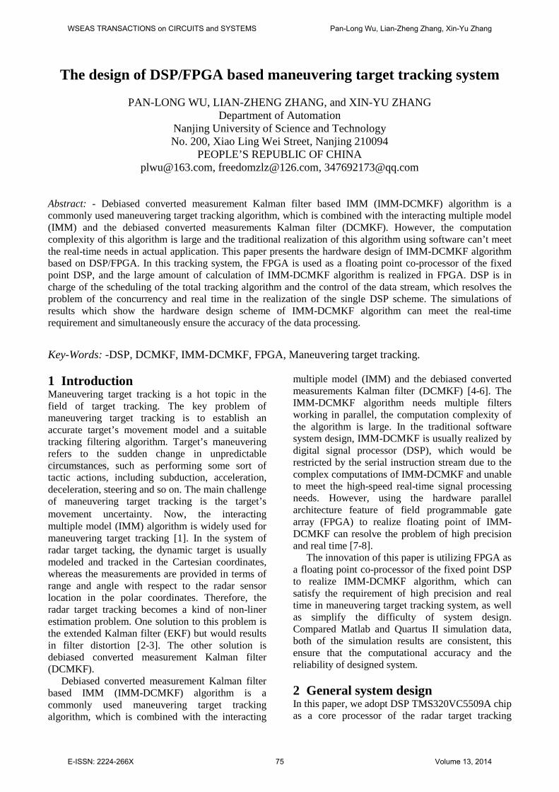
, ,x y z respectively. ( ), ( ), ( )x k y k z k denote the acceleration in the , ,x y z respectively. The CV model is used to describe the basic motion of the target, the CA model is used to describe target maneuver. The matrices 1( )F k ,
2 ( )F k , 1( )G k , 2 ( )G k , 1( )w k , 2 ( )w k are specified as follows
1
1 0 0 0 0 0 0 00 1 0 0 0 0 0 00 0 1 0 0 0 0 00 0 0 1 0 0 0 0 0
( ) 0 0 0 0 1 0 0 0 00 0 0 0 0 1 0 0 00 0 0 0 0 0 0 0 00 0 0 0 0 0 0 0 00 0 0 0 0 0 0 0 0
TT
T
F k
= ,
2
2
2
1
2 0 00 2 00 0 2
0 0( ) 0 0
0 00 0 00 0 00 0 0
TT
TT
G k TT
=
,1
1 2
3
w (k)=k
k
k
www
2
2
2
2
1 0 0 0 0 2 0 00 1 0 0 0 0 2 00 0 1 0 0 0 0 20 0 0 1 0 0 0 0
( ) 0 0 0 0 1 0 0 00 0 0 0 0 1 0 00 0 0 0 0 0 1 0 00 0 0 0 0 0 0 1 00 0 0 0 0 0 0 0 1
T TT T
T TT
F k TT
=
,
2
2
2
2
2 0 00 2 00 0 2
0 0( ) 0 0
0 01 0 00 1 00 0 1
TT
TT
G k TT
=
,1
2 2
3
w (k)=k
k
k
www
where, T is the radar sampling period. 1( )w k is the acceleration in the time step k , 2 ( )w k is the acceleration increment in the time step k .
1 2 3, ,k k kw w w are independent Gaussian white noise. Therefore, the measurement equation after
coordinate transformation is as follows:
WSEAS TRANSACTIONS on CIRCUITS and SYSTEMS Pan-Long Wu, Lian-Zheng Zhang, Xin-Yu Zhang
E-ISSN: 2224-266X 77 Volume 13, 2014

( ) ( ) ( )Z k HX k V k= + (2) 1 0 0 0 0 0 0 0 00 1 0 0 0 0 0 0 00 0 1 0 0 0 0 0 0
H =
(3)
where, ( ) ( ), ( ), ( )T
x y zV k v k v k v k = is zero mean
white noise, the corresponding covariance is ( )R k . 3.2 IMM-DCMKF algorithm The procedure of IMM-DCMKF algorithm is shown in Fig.5.
( )Z k
Measurements in the spherical coordinate
The debiased converted
measurements
Measurements in the Cartesian
coordinate
Model Interaction
Model Probability
Update
State Combination
filter
1( )M k
filter
2 ( )M k
filter
1ˆ ( 1| 1)X k k− − 2ˆ ( 1| 1)X k k− − rˆ ( 1| 1)X k k− −
1ˆ ( | )X k k 2ˆ ( | )X k k rˆ ( | )X k k ( )kµ ˆ ( | )X k k
( 1| 1)k kµ − −
( )kΛ
1ˆ ( 1| 1)OX k k− − 2ˆ ( 1| 1)OX k k− − rˆ ( 1| 1)OX k k− −
r ( )M k
Fig.5 Procedure of IMM-DCMKF algorithm The IMM-DCMKF algorithm consists of the following four steps. (a) Model interaction: Suppose there are r models, the transition probability from model i to model j is ijP .
11 12 1
21 22 2
1 2
r
r
r r rr
P P PP P P
P
P P P
=
(4)
Suppose ˆ ( 1| 1)jX k k− − is the state estimation of the filter j in the time step 1k − , ( 1| 1)jP k k− − is the state covariance matrix, 1( )ku j− is the probability of the model j , , 1,2,i j r= . Therefore, after interactive computing r filter input in the time step k the state vector is given as follows.
1| 11
ˆˆ ( 1 | 1) ( 1 | 1) ( | )r
oj jk k
iX k k X k k u i j− −
=
− − = − −∑ (5)
where
( ) ( ) ( )1| 1 1 11
1|r
k k ij k j ij kij
u i j P u i C P u iC− − − −
=
= =∑,.
1
'1| 1
( 1| 1)
ˆ{ ( 1| 1) [ ( 1| 1)
ˆˆ ( 1| 1)][ ( 1| 1)ˆ ( 1| 1)] } ( | )
=
− −
− −
= − − + − −
− − − − −
− − −
∑
oj
ri i
i
oj j
jk k
P k k
P k k X k k
X k k X k k
X k k u i j
(6)
(b) Model-conditioned filtering: Using ˆ ( 1| 1)ojX k k− − , ( 1| 1)ojP k k− − , the debiased converted measurement ( )R k , ( )Z k as the inputs of j model in the time step k , then the new state estimation ˆ ( | )jX k k and the corresponding estimation covariance ( | )jP k k can be achieved through Kalman filter.
cos cos( ) ( ) ( ) cos sin ( )
sin
m m m
m m m
m m
rZ c Z k k r k
r
η θµ η θ µ
η
= − = −
(7)
( ) [ , , ]x y z Tk k kkµ µ µ µ= (8)
( )
xx xy xzk k kyx yy yzk k kzx zy zzk k k
R R RR k R R R
R R R
=
(9)
The specific formula of ( )kµ and ( )R k can be found in reference [5]. (c) Model probability update: Defining the filter residuals of the model j is j
kv , the corresponding covariance is j
kS , then the likelihood of the model j is:
11 1exp ( ) '( )2| 2 |
j j j jk k k kj
k
v S vSπ
− Λ = − (10)
where ( ) ( ) ( )( ) ( ) ( ) ( )
ˆ | 1
| 1
j j jk
j j j jk
v Z k H k X k k
S H k P k k H k R k
= − − ′= − + .
The probability update of the model j is 1( ) j
k k ju j CC
= Λ
(11)
where
1
rjk j
jC C
=
= Λ∑ .
(d) State Combination: Finally, all the sub-model conditioned state estimates and covariances are probabilistically combined to find the overall estimate ˆ ( | )X k k and its covariance matrix ( | )P k k .
WSEAS TRANSACTIONS on CIRCUITS and SYSTEMS Pan-Long Wu, Lian-Zheng Zhang, Xin-Yu Zhang
E-ISSN: 2224-266X 78 Volume 13, 2014

1
ˆ (̂ | ) ( | ) ( )r
jk
jX k k X k k u j
=
=∑
(12)
1
ˆ( | ) { ( | ) [ ( | )
ˆˆˆ ( | )][ ( | ) ( | )]'}
rj j
j
j jk
P k k P k k X k k
X k k X k k X k k u=
= +
− −
∑ (13)
4 FPGA realization of IMM-DCMKF algorithm In this paper, the MATLAB auxiliary Quartus II design method is used to validate the performance and accuracy of the FPGA realization of IMM-DCMKF algorithm. Firstly, the IMM-DCMKF algorithm is decomposed into the scalar form, and realized by MATLAB to validate the correctness of the decomposition. Then the IMM-DCMKF algorithm is implemented by using the VHDL language according to the floating-point scalar programming, and simulated on the Quartus II platform. The floating-point data of Quartus II simulation results are converted to decimal format data using the floating-point conversion software (IEE.exe). Finally, the decimal format data are compared with MATLAB simulation results to verify the correctness of the FPGA design. 4.1 Block-based FPGA architecture design Quartus II software-based FPGA design processes include top-down, bottom-up and block-based design [10-12]. In this paper, the block-based design process is adopted. The bottom-level is designed by VHDL language, the top-level is designed by schematic capture. The input and synthesis tools of Quartus II are used to design and synthesize the various modules, and each module is integrated into the top-level design in the Quartus II software. The design process including circuit design with VHDL input, functional simulation, integrated, comprehensive post-simulation after routing the main steps of the simulation and verification. Fig.6 shows the overall structure diagram of the FPGA design of the IMM-DCMKF algorithm. The figure includes a total of 28 modules, 22 modules designed by VHDL language, 3 first in first out (FIFO) modules built-in FPGA, and 3 double-selection modules. Three FIFO modules are used to store the updated state values, the updated covariance values and the model probability updated values, respectively. These stored data are prepared for the next frame data filtering. Three double-selection modules are used for the initial value selected of
state, covariance, model probability and the loop filtering value, respectively. At the first frame, the target spherical coordinates value, the initial state value, initial covariance value and the initial value of the model probability are transferred. Starting from the second frame, only the target spherical coordinates values are transferred.
The module to extract
target information
Model probability prediction and mixed weight
module
Mixed covarianc
e estimation module
Mixed state
estimation module
The trigonometric
function module
The angle information
square module
The one step state
prediction
module
The state average true bias module
The Covariance
average true bias module
The Gain
matrix modul
e
The state updat
e modul
e
The module between the spherical and
Cartesian coordinates
of conversion
The one step
prediction module
New modu
le
The filtering error
covariance update module
State interaction output module
The model Probability
Update calculation module 1
The model Probability
Update calculation module 2
The FIFO module of stores the error
Probability updating values
The FIFO module of stores the error state updating values
The FIFO module of stores the
error covariance updating values
The inverse matrix
module 1 of measuremen
t residuals
The inverse matrix
module 2 of measuremen
t residuals
The inverse matrix
module 3 of
measurement
residuals
MUX1
MUX2
MUX3
angle
distance
The target information
of spherical
coordinates
trigonometric function
The target information
of Cartesian
coordinates
Filter output
mixed
weight
Model probability
prediction
The initial value of
covariance
initial value of state values
The initial value of
Probability model
Covariance in circulation
The state values in the
circulation
Probability model in
the circulation
Measurement of residual value of the inverse matrix array
The measurement residual matrix
determinant
The output of model uses the probabilistic
The model Probability
Update calculation module 1
Fig.6 Hierarchical design of IMM-DCMKF algorithm based on FPGA
Altera’ Cyclone Ⅲ series EP3SL200H780 chip is
chosen to realize IMM-DCMKF algorithm on Quartus II platform. The floating point number based arithmetic operation modules built in Quartus II consist of addition, subtraction, multiplication and division. The basic floating point number operation modules are instantiated and the corresponding parameters are set accordingly in the VHDL code design, which would improve the design performance, shorten the design time and simply the data path realization of floating point data [13].The synchronous clock scheme is introduced into top-level schematic diagram during the FPGA design of the IMM-DCMKF algorithm. In order to make multiple modules coordinated, the enable signal is set. The state of enable signal of each module is detected to determine whether the corresponding operation can be implemented [14]. In IMM-DCMKF algorithm some modules need the result of the previous modules. Therefore, the IMM-DCMKF algorithm can not all parallel computing, In this paper, we adopt parallel computing in parallel computing modules. Meanwhile, enabled signal is detected in unable parallel computing modules to determine the appropriate operation. The pipeline technology is used within each module to improve operation speed.
WSEAS TRANSACTIONS on CIRCUITS and SYSTEMS Pan-Long Wu, Lian-Zheng Zhang, Xin-Yu Zhang
E-ISSN: 2224-266X 79 Volume 13, 2014
4.2 Modules design of IMM-DCMKF FPGA can only operate add, subtract, multiply, divide and other simple calculation, can not call function to carry out complex calculations. Therefore, IMM-DCMKF algorithm needs to decompose into the scalar form, which can facilitate the realization of the code, and effectively improve the FPGA resource utilization [15]. IMM-DCMKF algorithm needs to be decomposed into simple add, subtract, multiply, divide, index and root operation, these operation can be realized by the IP computing modules which built in the Quartus II. Floating-point arithmetic design based on FPGA will take up more resources. Therefore, the time multiplexed design idea is used in basic arithmetic unit [16].
In order to realize a balance between speed and resources of the FPGA, and save resources of floating-point multiplier, this paper applies the following three optimizations. 1) On the basis of the system parallel computing, the CV model and the CA model are sequence filtered, and time division multiplexed. Firstly, the CV model is filtered, then the CA model is filtered. 2) The merging of similar items to reduce the use of the computing unit. 3) In the inner of computing modules, the previous-class items which doe not participate in the operation, are delayed corresponding cycles by using the registers, and then participate in the next-class computing.
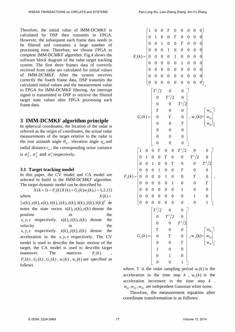
Taking the state interactive output module as example, the Oex denotes the interaction output ˆ ( | )X k k , Usx1 and Usx2 denote the CV model and CA model updated state ˆ ( | )iX k k , respectively, Mp denotes the model probability ( )k iµ .Therefore,(12) can be decomposed into the following scalar form:
0 0 1 0 2
1 1 1 1 2
2 2 1 2 2
3 3 1 3 2
4 4 1 4 2
5 5 1 5 2
1 * 2 *1 * 2 *1 * 2 *1 * 2 *1 * 2 *1 * 2 *
= += += += += += +
Oex Usx Mp Usx MpOex Usx Mp Usx MpOex Usx Mp Usx MpOex Usx Mp Usx MpOex Usx Mp Usx MpOex Usx Mp Usx Mp
6 6 2
7 7 2
8 8 2
2 *2 *2 *
===
Oex Usx MpOex Usx MpOex Usx Mp
.
reg_usx0 reg_mp0 reg_usx1 reg_mp0 reg_usx2 reg_mp0 reg_usx3 reg_mp0 reg_usx4 reg_mp0 reg_usx5 reg_mp0 0 0 0 0 0 0
reg_usx6 reg_mp1 reg_usx7 reg_mp1 reg_usx8 reg_mp1 reg_usx9 reg_mp1 reg_usx10 reg_mp1 reg_usx11 reg_mp1 reg_usx12 reg_mp1 reg_usx13 reg_mp1 reg usx14 reg mp1
data distribution module
RAMmemor
y
Pipeline timing
of addition
Mp
Usx
Oex
Step1
Step2
Step3
Step4
Step5
Step1
Step2
Step3
Step4
Step5
Step1
Step2
Step3
Step4
Step5
Step1
Step2
Step3
Step4
Step5
Step1
Step2
Step3
Step4
Step5
Step1
Step2
Step3
Step4
Step5
pipeline timing of multiplier
Fig.7 Structural chart of state interaction output
module
Fig.7 is the block diagram of the state interactive output module. Firstly, the received data of the module are stored in the synchronous RAM memory of FPGA when module detects the correct enable signal. Then, the data processing time of previous-class and next-class are equalized through the rational design of data distribution module. The output of previous-class directly import into the next-class input stage to participate in the pipelined operations. In Fig.7, the pipeline timing sequence of addition is similar to the pipeline timing sequence of multiplier. The state interactive output module needs a total of 2 multipliers and 1 adder. In this paper, the period parameters of floating point addition and multiplication units are set respectively, which are set as 7 and 5clock cycles in library parameter module (LPM) of Quartus II.
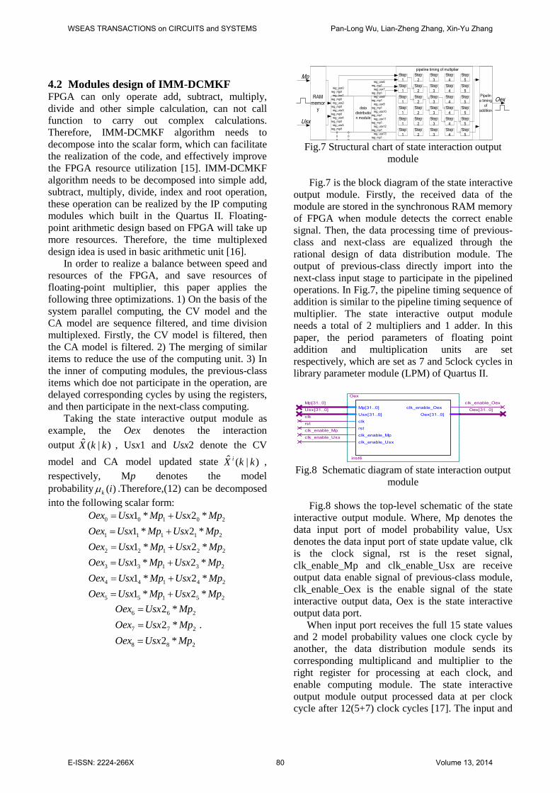
Mp[31..0]
Usx[31..0]
clk
rst
clk_enable_Mp
clk_enable_Usx
clk_enable_Oex
Oex[31..0]
Oex
inst6
Mp[31..0]
Usx[31..0]
clk
rst
clk_enable_Mp
clk_enable_Usx
clk_enable_Oex
Oex[31..0]
Fig.8 Schematic diagram of state interaction output
module Fig.8 shows the top-level schematic of the state
interactive output module. Where, Mp denotes the data input port of model probability value, Usx denotes the data input port of state update value, clk is the clock signal, rst is the reset signal, clk_enable_Mp and clk_enable_Usx are receive output data enable signal of previous-class module, clk_enable_Oex is the enable signal of the state interactive output data, Oex is the state interactive output data port.
When input port receives the full 15 state values and 2 model probability values one clock cycle by another, the data distribution module sends its corresponding multiplicand and multiplier to the right register for processing at each clock, and enable computing module. The state interactive output module output processed data at per clock cycle after 12(5+7) clock cycles [17]. The input and
WSEAS TRANSACTIONS on CIRCUITS and SYSTEMS Pan-Long Wu, Lian-Zheng Zhang, Xin-Yu Zhang
E-ISSN: 2224-266X 80 Volume 13, 2014
output ports design of other computing module are similar.
Taking the model probability update module as another example, because model probability update module contains addition, multiplication, division and square root operations, its calculation is very complex. In order to facilitate the design of VHDL language, the (10) and (11) will be transformed into scalar form. Afterwards they will be decomposed into three modules, respectively. The three modules are defined as model probability update module 1, model probability update module 2 and model probability update module 3. In the design process, the output intermediate variable of model probability update module 1is Msme , the output intermediate variables of model probability update module 2 is Ml .
RAMmemory
Zk
S_1
Data distribution
module
CLK
CLK
CLK
CLK
CLK
CLK
CLK
Msme
pipeline operation module
Data distribu
tion module
7
CLK
CLK
CLK
CLK
CLK
CLK
CLK
CLK
CLK
CLK
CLK
CLK
7 7 7
exp
CLK CLK CLK
CLK CLK
CLK
pipeline operation module
Fig.9 The design block diagram of the model probability update module1
Fig.9 is the design block diagram of the model
probability update module 1, it uses three floating-point multipliers, six floating-point adders and a floating-point exponentiation. During the design of pipeline operation module, in order to make the design data synchronization, using registers delay 5 and 7 clock cycles involved in the subordinate operation for the items, which are not involved in the multiplication and addition operations.
RAMmemor
y
Msme
Data distribution
module
CLK
CLK
CLK
CLKMl
pipeline operation module
CLKCLK
S
5
sqrt
CLK
16
CLK
Fig.10The design block diagram of the model probability update module2
Fig.10 is the design block diagram of the model
probability update module 2,it uses 1 floating-point multiplier, 1 floating-point divider and 1 root operation. In the design of pipeline operation module, in order to make the design data synchronization, using registers delay 5 and 16 clock cycles involved in the subordinate operation for the items, which are not involved in the multiplication and addition operations.
RAMmemor
yPmp
Data distribution
module
CLK
CLK
CLK
CLK
CLK
CLK
CLK
Mp
pipeline operation module
Data distribut
ion module
CLK
CLK
CLK
pipeline operation module
Ml
7
7CLK
CLK
Fig.11 The design block diagram of the model
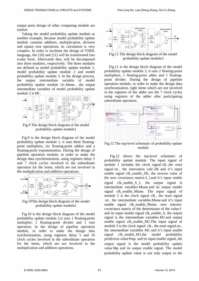
probability update module3
Fig.11 is the design block diagram of the model probability update module 3, it uses 2 floating-point multipliers, 1 floating-point adder and 1 floating-point divider. During the design of pipeline operation module, in order to make the design data synchronization, right items which are not involved in the registers of the adder use the 7 clock cycles using registers of the adder after participating subordinate operation.
Fig.12 The top-level schematic of probability update
module Fig.12 shows the top-level schematic of
probability update module. The input signal of module 1 includes the clock signal clk ,the reset signal rst , the innovation vale ZK and it’s input enable signal clk_enable_ZK, the inverse value of the new covariance matrix _1S and it’s input enable signal clk_enable_S_1, the output signal is intermediate variables Msme and its output enable signal clk_enable_Msme. The input signal of module 2 is the clock signal clk , the reset signal rst , the intermediate variables Msme and it’s input enable signal clk_enable_Msme, new interest-covariance matrix of the determinant of the value S and its input enable signal clk_enable_S, the output signal is the intermediate variables M1 and output enable signal clk_enable_M1.The input signal of module 3 is the clock signal clk , the reset signal rst , the intermediate variables M1 and it’s input enable signal clk_enable_M1,the model probability prediction value Pmp and its input enable signal, the output signal is the model probability update value Mp and its output enable signal. The model probability update value is not only output to the
WSEAS TRANSACTIONS on CIRCUITS and SYSTEMS Pan-Long Wu, Lian-Zheng Zhang, Xin-Yu Zhang
E-ISSN: 2224-266X 81 Volume 13, 2014

state interaction module Oex , but also output to the FIFO module to storage model probability update value for the next data loop. Therefore, there are two output enable signals, clk_enable_Mp_to_Oex and clk_enable_Mp_to_FIFO. The enable signal clk_enable_Mp_to_FIFO will be closed when all the model probability update values are stored in the FIFO. 4.3 Simulation waveforms of FPGA Fig.13 and Fig.14 are intercepted part of the input and output simulation waveforms. Wherein, Fig.13 is the initial value and the first frame of data input waveform, the initial value including the initial state, the initial covariance and the initial model probability. The first frame data are the radial distance of the target, azimuth and elevation angle. Fig.14 is the state interaction output waveforms of the first frame data. If clock cycle is 40ns, one IMM-DCMKF filter cycle needs 22.88us.Fig.13 and Fig.14 verify the timing simulation delay is very small.
Fig.13Initial value and the first frame of data input
waveform
Fig.14The state of interaction output waveform of
the first frame of data 5 Simulation and results
Fig.15Hardware circuit board
Fig.15 shows the hardware circuit board, this subsystem is composed of DSP, FPGA, SDRAM, FLASH, SD card and other components. The power supply for the circuit board of DSP subsystem is DC 5V. The power supply for the circuit board of FPGA subsystem is 24V DC. Firstly, the power convert chip converts the DC 24V to DC 5V, then supply to the DSP subsystem through the connection. In the FPGA subsystem, DC 5V is converted to 3.3V, 2.5V and 1.2V respectively.
In this section, a simulation scenario is presented to track a maneuvering target. The parameters of target are given as follows: The initial position is (10000 ,6000 ,4000 )m m m , the initial velocity is ( 300 / , 300 / , 100 / )m s m s m s− − − , The sampling rate is 10T ms= , the target flying trajectory is shown in Fig.16. From t=0-5s, target flies at constant velocity, from t=5-30s, it makes ‘S’ shaped acceleration maneuver, from 30-35s it flies at constant velocity. The noise covariance of the measured distance r, elevation η and azimuth θ are
2 21 / 36r mσ = , 2 2 2/ 72900radησ π= , 2 2 2/ 32400radθσ π= . The model transition
probability and the model initial probability are 0.99 0.010.01 0.99
P =
, [ ]0.5 0.5µ = . In the process of
simulation, the IMM-DCMKF algorithm is realized respectively in FPGA and Matlab platform using the same measurements. Fig.17-Fig.19 are the position comparison in X, Y, Z directions separately. From Fig.17-Fig.19, it is easily can be seen that the IMM-DCMKF is capable of denoising and smoothing for target position. From Figs 16-19, it can be seen that the FPGA simulation results are basically consistent
WSEAS TRANSACTIONS on CIRCUITS and SYSTEMS Pan-Long Wu, Lian-Zheng Zhang, Xin-Yu Zhang
E-ISSN: 2224-266X 82 Volume 13, 2014
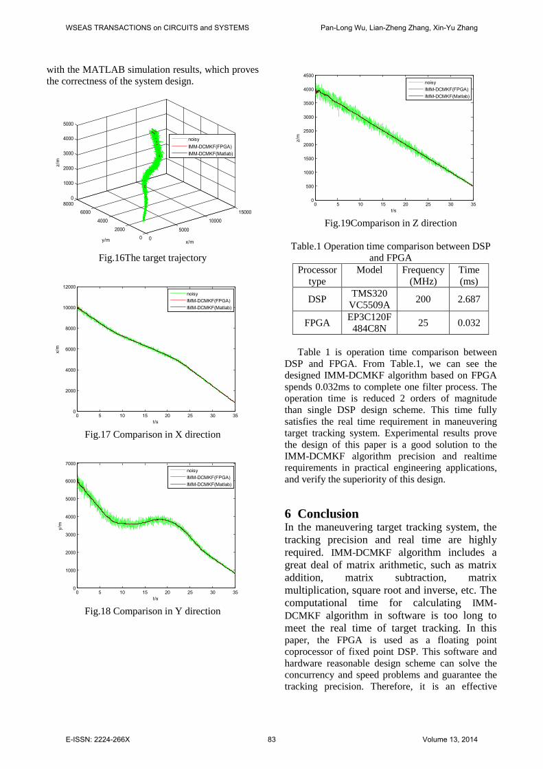
with the MATLAB simulation results, which proves the correctness of the system design.
0
5000
10000
15000
02000
4000
60008000
0
1000
2000
3000
4000
5000
x/my/m
z/m
noisyIMM-DCMKF(FPGA)IMM-DCMKF(Matlab)
Fig.16The target trajectory
0 5 10 15 20 25 30 350
2000
4000
6000
8000
10000
12000
t/s
x/m
noisyIMM-DCMKF(FPGA)IMM-DCMKF(Matlab)
Fig.17 Comparison in X direction
0 5 10 15 20 25 30 350
1000
2000
3000
4000
5000
6000
7000
t/s
y/m
noisyIMM-DCMKF(FPGA)IMM-DCMKF(Matlab)
Fig.18 Comparison in Y direction
0 5 10 15 20 25 30 350
500
1000
1500
2000
2500
3000
3500
4000
4500
t/s
z/m
noisyIMM-DCMKF(FPGA)IMM-DCMKF(Matlab)
Fig.19Comparison in Z direction
Table.1 Operation time comparison between DSP
and FPGA Processor
type Model Frequency
(MHz) Time (ms)
DSP TMS320 VC5509A 200 2.687
FPGA EP3C120F 484C8N 25 0.032
Table 1 is operation time comparison between
DSP and FPGA. From Table.1, we can see the designed IMM-DCMKF algorithm based on FPGA spends 0.032ms to complete one filter process. The operation time is reduced 2 orders of magnitude than single DSP design scheme. This time fully satisfies the real time requirement in maneuvering target tracking system. Experimental results prove the design of this paper is a good solution to the IMM-DCMKF algorithm precision and realtime requirements in practical engineering applications, and verify the superiority of this design.
6 Conclusion In the maneuvering target tracking system, the tracking precision and real time are highly required. IMM-DCMKF algorithm includes a great deal of matrix arithmetic, such as matrix addition, matrix subtraction, matrix multiplication, square root and inverse, etc. The computational time for calculating IMM-DCMKF algorithm in software is too long to meet the real time of target tracking. In this paper, the FPGA is used as a floating point coprocessor of fixed point DSP. This software and hardware reasonable design scheme can solve the concurrency and speed problems and guarantee the tracking precision. Therefore, it is an effective
WSEAS TRANSACTIONS on CIRCUITS and SYSTEMS Pan-Long Wu, Lian-Zheng Zhang, Xin-Yu Zhang
E-ISSN: 2224-266X 83 Volume 13, 2014
approach to complete maneuvering target tracking algorithm. The design based on FPGA has large degree flexibility for programming, updates codes at any time, and largely reduces the research cost. Acknowledgement This work is partially supported by the National Nature Science Foundation of China (NO. 61104196), Natural Science Foundation of Jiangsu Province (No. BK20131352), “Zijin star” Research Funding (NO. AB41381). References: [1] H. L. Han, X. C. Zhou, G. S Yuan, An
improved IMM algorithm of 3D maneuvering target tracking, Radar& ECM, Vol.30, No.4, 2010, pp.29-32.
[2] P. L. Wu,Y. D. Cai, B. B. Wang, Satellite bearings-only tracking using extended Kalman particle filter, Infrared and Laser Engineering, Vol.40, No.10, 2011, pp.2008-2013.
[3] M. Alipakzad, Kalman filter design for time delay systems, WSEAS Transactions on System,Vol.11,No.10,2012,pp.551-560.
[4] D. L. Liu, H. Q. Wang, X. Li, Maneuvering target tracking with non-linear measuring equations based on IMM algorithm, Electronics Optics & Control, Vol.9, No.4, 2002, pp.19-23.
[5] P. L. Wu, B. B. Wang, C. H. Ji, Design and realization of short range defence radar target tracking system based on DSP/FPGA, WSEAS Transactions on System,Vol.10,No.11,2011,pp.379-380.
[6] C. H. Ji, P. L. Wu, S. Peng, B. B. Wang, Debiased converted measurement IMM for maneuvering target tracking algorithm realized with hardware, Electronics optics & control, Vol.20, No.4, 2013, pp.51-55.
[7] C. W. Wang, H. N. Cai, J. H. Wu, Altera FPGA/CPLD design (Basics), Posts & telecom press, 2011.
[8] S. Z. Zhong, C. H. Hou, C. A. Yang, Optimized design of matrix multiplier based on FPGA, Electronic Measurement Technology,Vol.31, No.2, 2008, pp.95-102.
[9] L. Z Zhang, P. L. Wu, X. Y. Zhang, Air defense missile detonation delay control based on FPGA/DSP, WSEAS Transactions on System,Vol. 12, No. 4, 2013, pp. 202-211.
[10] N. N. Zhou, Y. L. Chen, A. Q. Li, Design and implementation of floating point calculator based on FPGA technology, Computer Engineer and Design, Vol.26, No.6, 2005, pp.1578-1581.
[11] K. P. Chen, S. L. Zhu, Y. S. Lin, Implementation of Pseudo-Linear Kalman Filter for Bearings-only Target Tracking on FPGA, Fire Control & Command Control, Vol.35, No.3, 2010, pp.25-28.
[12] C. R. Lee, Z. Salcic, High-performance FPGA-based Implementation of Kalman Filter, Mircroprocessors and Microsystems, Vol.21, No.4, 1997, pp.257-265.
[13] S. M. Shalinie, Design and analysis of customized embedded Kalman filter, IE(I) Journal-CP, Vol.88, No.5, 2007, pp.39-42.
[14] H. P. Jiang, B. Li, Z. K. Shen, Design of adaptive Kalman filter based on FPGA implementation,Infrared and Laser Engineering, Vol.34, No.1, 2005, pp.89-92.
[15] G. Chen, L. Guo. The FPGA Implementation of Kalman Filter. Proceedings of the 5th WSEAS Int. Conf. on Signal Processing, 2005, pp.61-65.
[16] R. Pasricha, S. Sharma. An FPGA-based design of fixed-point Kalman filter, DSP Journal. Vol.9, No.1, 2009, pp.1-9
[17] A. Bigdeli, M. Biglari-Abhari, Z. Salcic, Y. T. Lai, A new pipelined systolic array-based architecture for matrix inversion in FPGAs with Kalman filter case study, EURASIP Journal on Applied Signal Processing, Vol.2006, Article ID 89186, 2006, pp.1-12.
WSEAS TRANSACTIONS on CIRCUITS and SYSTEMS Pan-Long Wu, Lian-Zheng Zhang, Xin-Yu Zhang
E-ISSN: 2224-266X 84 Volume 13, 2014