Embed Size (px)
DESCRIPTION
The Design of SiGe pnp HBTs. At present, SiGe technology development is almost exclusively centered on npn SiGe HBTs. - PowerPoint PPT Presentation
Citation preview
The Design of SiGe pnp HBTs
At present, SiGe technology development is almost exclusively centered on npn SiGe HBTs.
However, for high-speed analog and mixed-signal circuit applications, a complementary (npn+pnp) bipolar technology offers signification performance advantages over an npn-only technology .
for example : Push-pull circuits
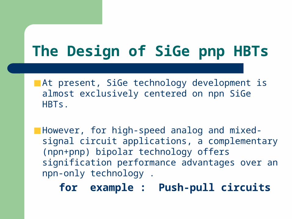
Push-pull circuits
Iv
-VCC
+VCC
RL
OvClass B output stage
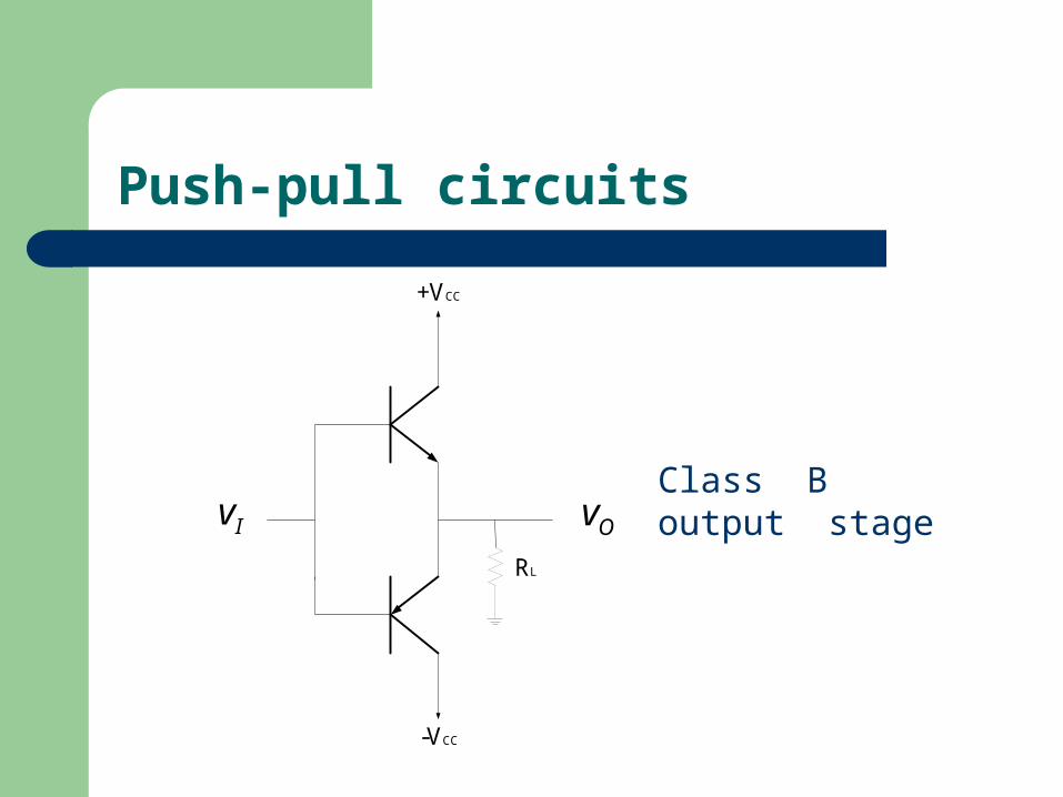
NPN and PNP of Si BJTs
Performance : npn Si BJTs > pnp Si BJTs
BJT) Si pnp a of base type(Nholeμ
BJT) Sinpn an of base type-(Pele
μ todue n
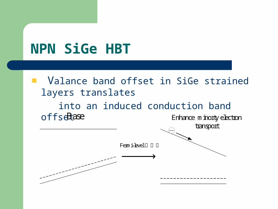
NPN SiGe HBT
Valance band offset in SiGe strained layers translates
into an induced conduction band offset
Enhance minorty electron transport
Base
Fermi-level 被拉平
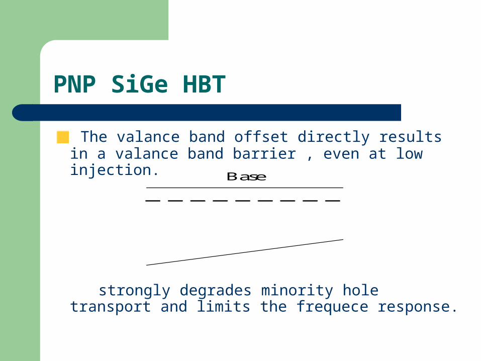
PNP SiGe HBT
The valance band offset directly results in a valance band barrier , even at low injection.
strongly degrades minority hole transport and limits the frequece response.
Base
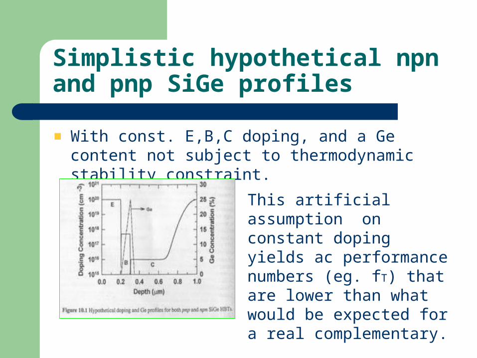
Simplistic hypothetical npn and pnp SiGe profiles
With const. E,B,C doping, and a Ge content not subject to thermodynamic stability constraint.
This artificial assumption on constant doping yields ac performance numbers (eg. fT) that are lower than what would be expected for a real complementary.
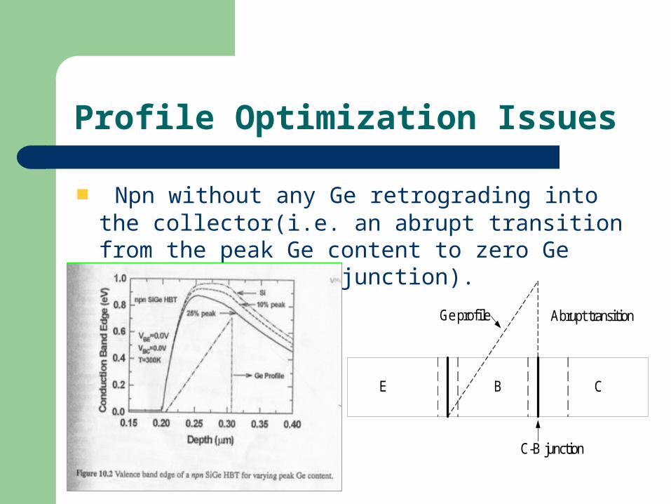
Profile Optimization Issues
Npn without any Ge retrograding into the collector(i.e. an abrupt transition from the peak Ge content to zero Ge content in the CB junction).
C-B junction
Abrupt transition
E B C
Ge profile
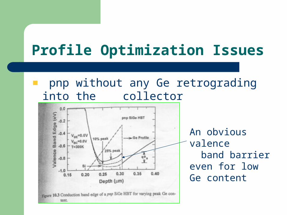
Profile Optimization Issues
pnp without any Ge retrograding into the collector
An obvious valence band barrier even for low Ge content
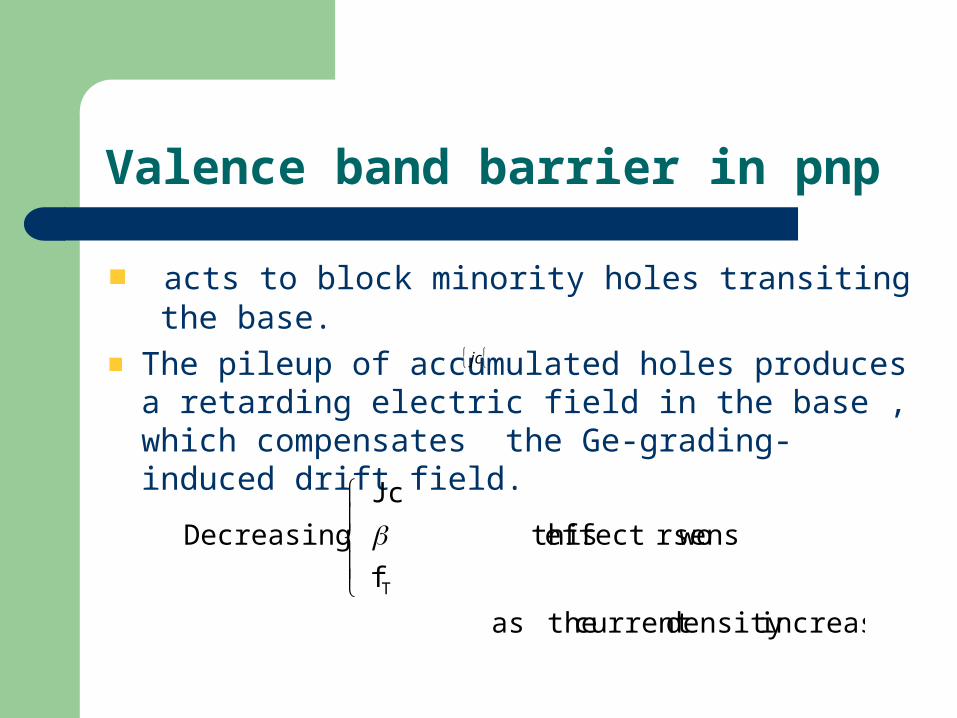
Valence band barrier in pnp
acts to block minority holes transiting the base.
The pileup of accumulated holes produces a retarding electric field in the base , which compensates the Ge-grading-induced drift field.
jc
increasesdensity current theas
rsenseffect wo this
f
Jc
Decreasing
T
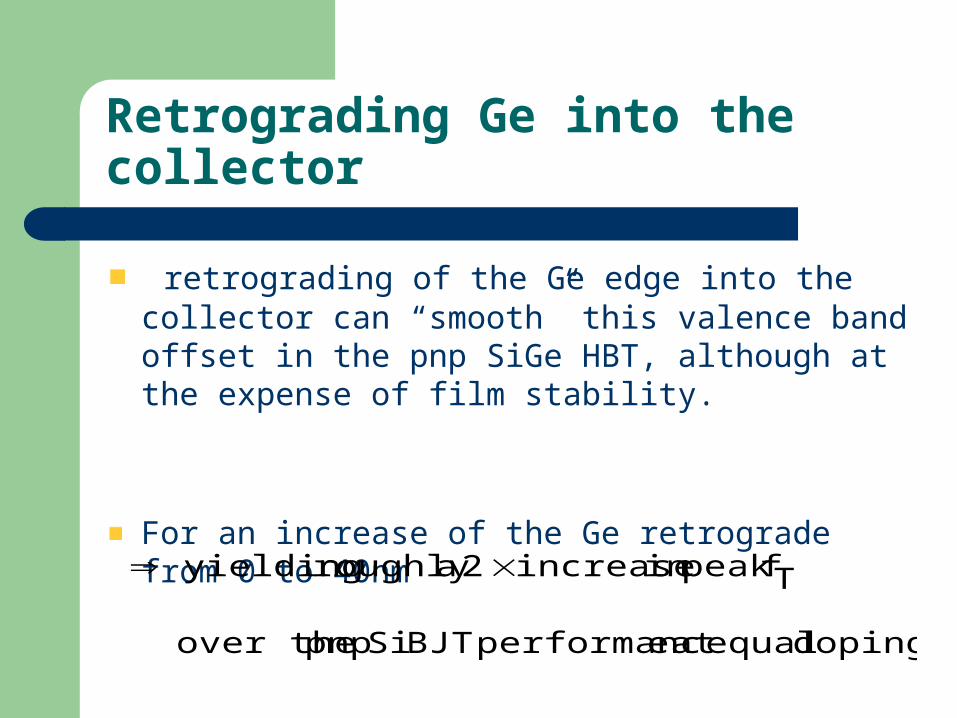
Retrograding Ge into the collector
retrograding of the Ge edge into the collector can “smooth” this valence band offset in the pnp SiGe HBT, although at the expense of film stability.
For an increase of the Ge retrograde from 0 to 40nm
doping. equalat eperformanc BJT Si pnp over the
Tfpeak in increase 2 aroughly yielding
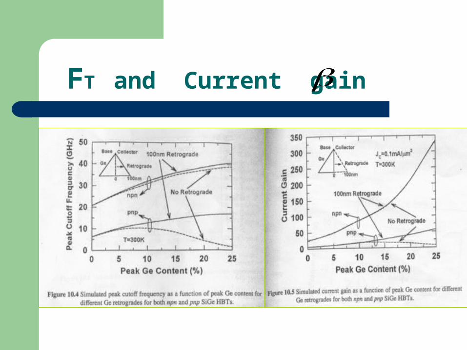
FT and Current gain
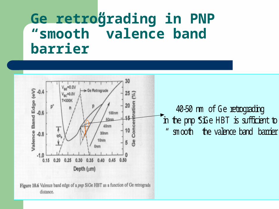
Ge retrograding in PNP “smooth” valence band barrier
40-50 nm of Ge retrograding in the pnp SiGe HBT is sufficient to “ smooth” the valence band barrier
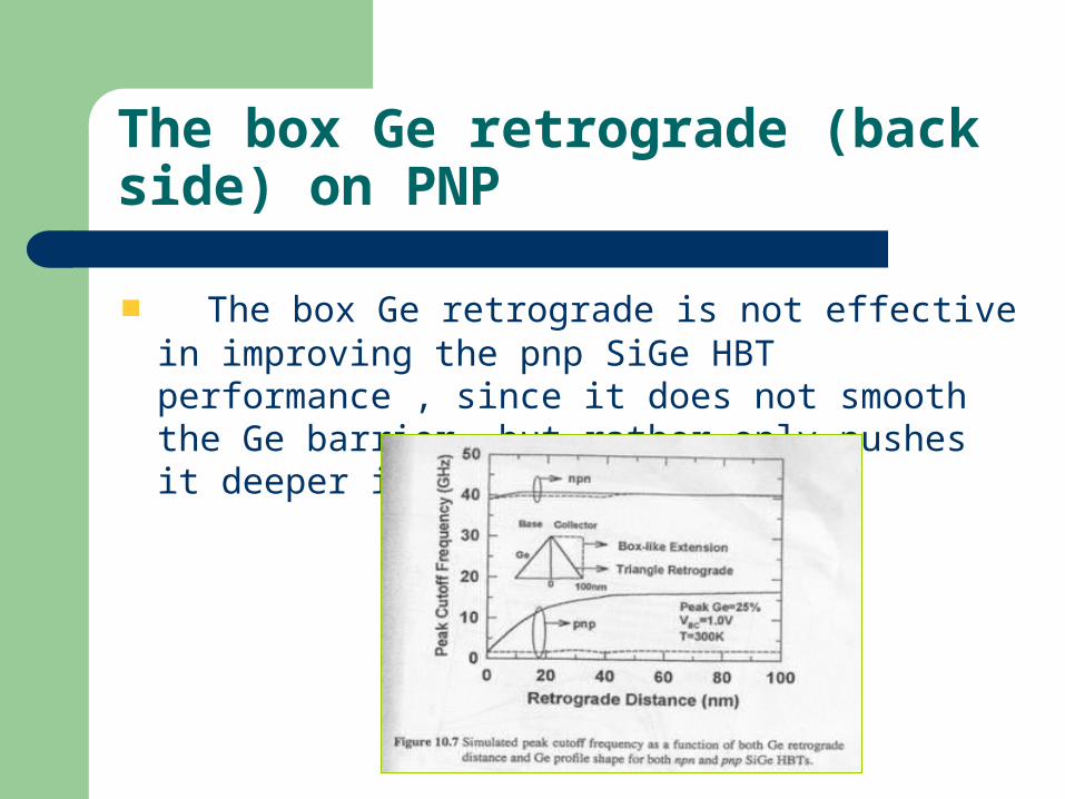
The box Ge retrograde (back side) on PNP
The box Ge retrograde is not effective in improving the pnp SiGe HBT performance , since it does not smooth the Ge barrier, but rather only pushes it deeper into collector
The effects of Ge retrograding on NPN
The effects of Ge retrograde on the npn SiGe HBT performance ------- minor, while the film stability is worse due to the additional Ge content.
So, we know using one Ge profile design for both npn and pnp SiGe HBTs is not optimum for high peak Ge content values.
Stability Constraints in PNP SiGe HBTs
The total amount of Ge that can be put into a given SiGe HBT -----limited by the thermodynamic stability.
Above the critical thickness the strain in
the SiGe film relaxes generating defects.
The empirical critical thickness of a SiGe multilayer
with a top-layer Si cap
----- approximately 4x the theoretical
stability result of Matthews and Blakeslee
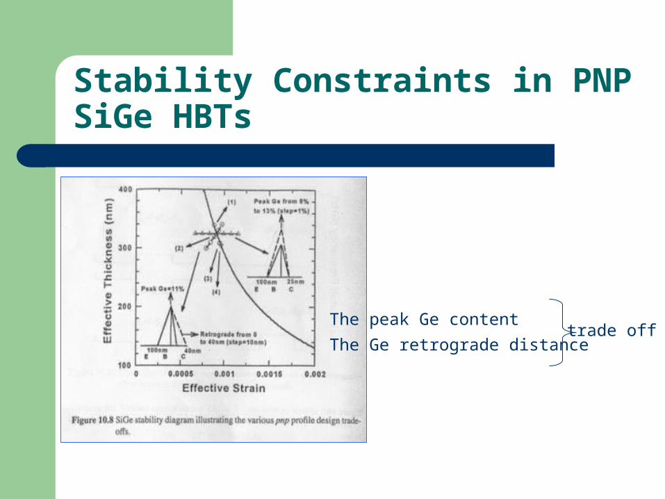
Stability Constraints in PNP SiGe HBTs
The peak Ge content
The Ge retrograde distance trade off
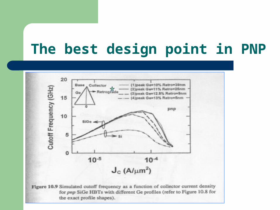
The best design point in PNP
Similar exercise for the npn
For npn SiGe HBT , the ac performance is not sensitive to the SiGe profile shapes used.
So the same Ge profile may be used for both pnp and npn SiGe HBTs.
being advantageous from a
fabrication viewpoint.
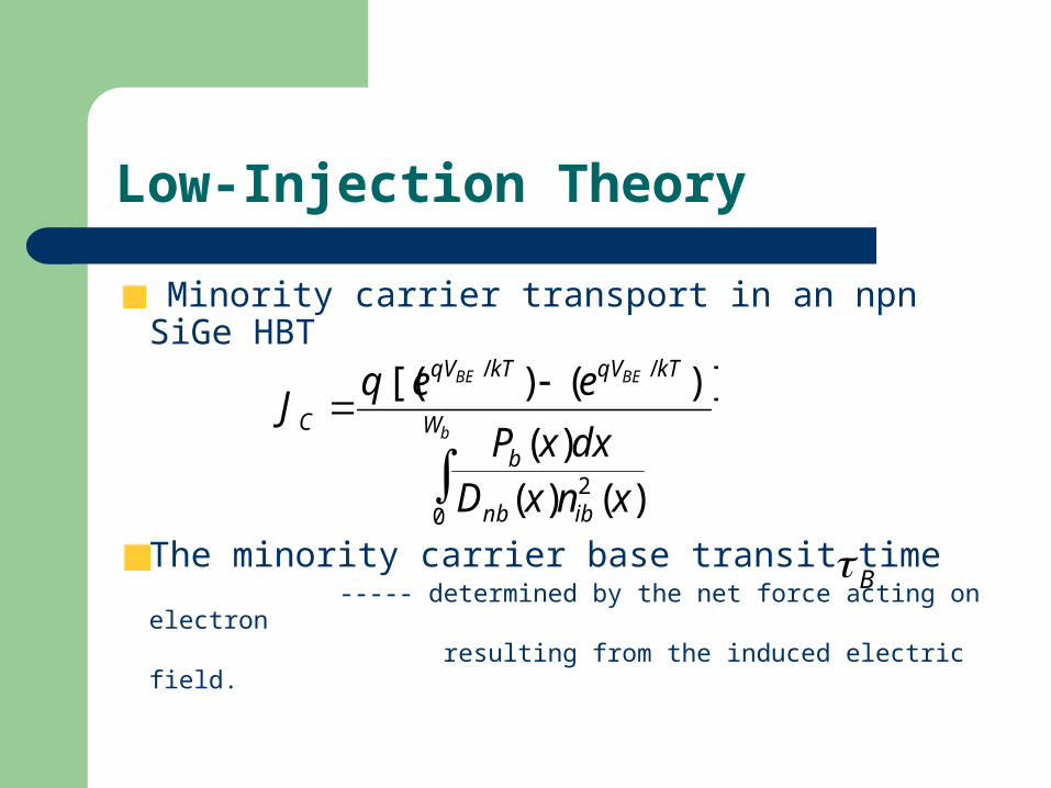
Low-Injection Theory
Minority carrier transport in an npn SiGe HBT
The minority carrier base transit time ----- determined by the net force acting on electron
resulting from the induced electric field.
b
BEBE
W
ibnb
b
kTqVkTqV
C
xnxDdxxP
eeqJ
02
//
)()()(
)]()[(
B
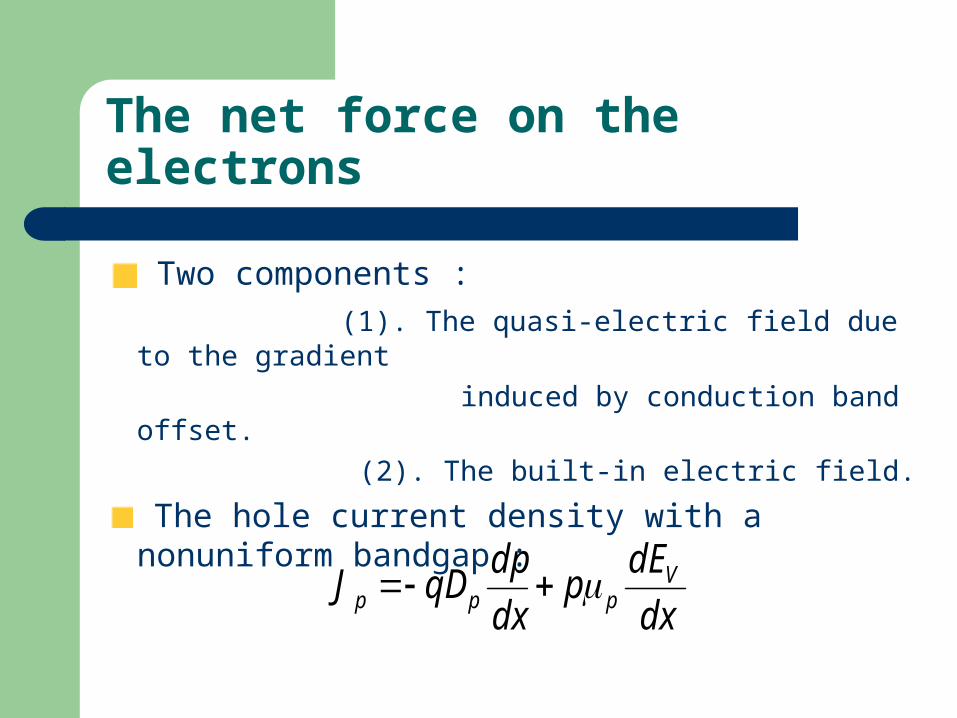
The net force on the electrons
Two components :
(1). The quasi-electric field due to the gradient
induced by conduction band offset.
(2). The built-in electric field.
The hole current density with a nonuniform bandgap :
dx
dEp
dx
dpqDJ V
ppp
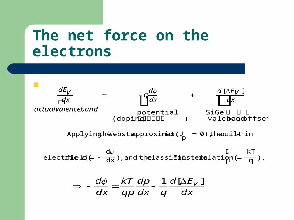
The net force on the electrons
offset band valence SiGe
][
) (doping potential 的起引不均勻所造成
dxVEd
dx
dq
bandvalenceactual
dxVdE
).q
kT
μ
Drelation(Einsteinclassical theand, )dx
dfield(εelectric
inbuiltthe0),p
(Jion approximat Webster theApplying
dx
Ed
qdx
dp
qp
kT
dx
d V ][1
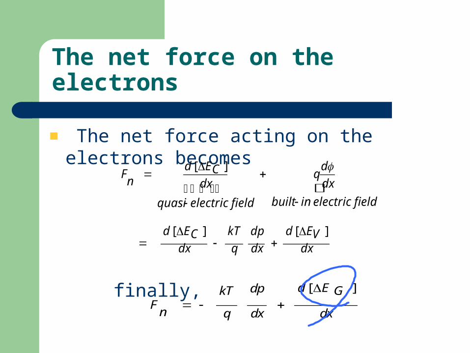
The net force acting on the electrons becomes
finally,
The net force on the electrons
dxVEd
dx
dp
q
kT
dxCEd
fieldelectricinbuilt
dx
dq
fieldelectricquasi
dxCEd
nF
][][
][
dx
GEd
dx
dp
q
kT
nF
][
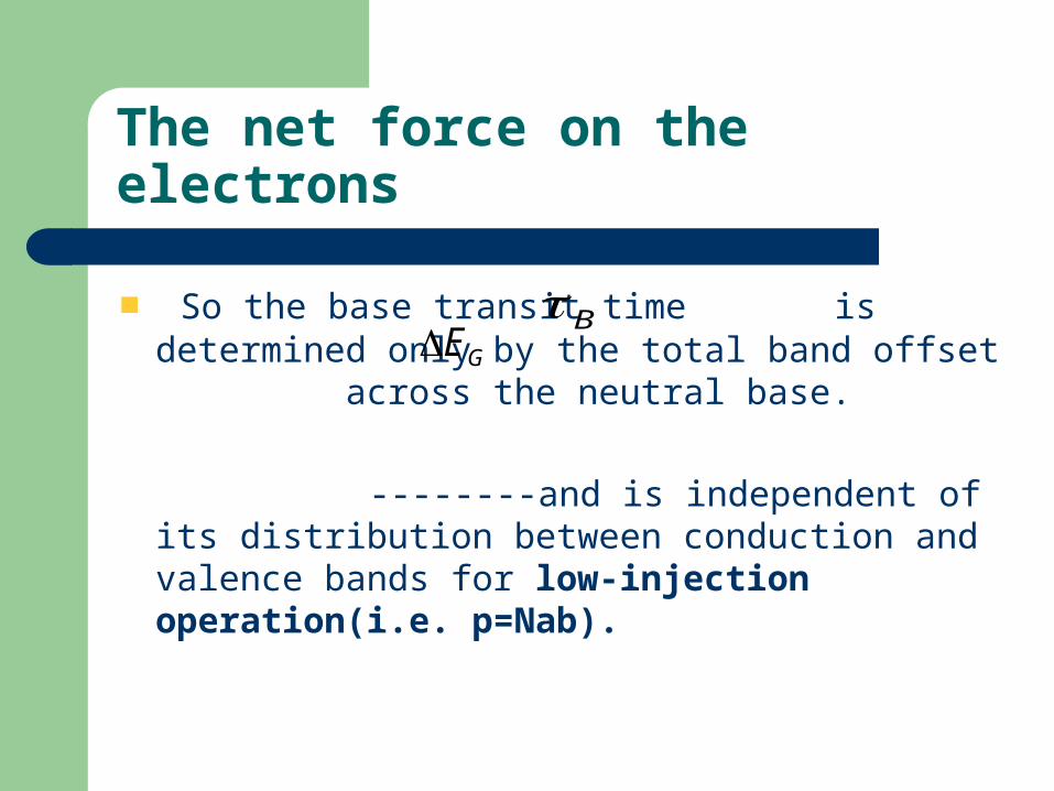
The net force on the electrons
So the base transit time is determined only by the total band offset across the neutral base.
--------and is independent of its distribution between conduction and valence bands for low-injection operation(i.e. p=Nab).
BGE
Impact of High Injection
To shed light on this issue, we consider the following four representative band offset distributions(band alignments) :
. off-rollfrequency cutoff affect thecan
VE
CE
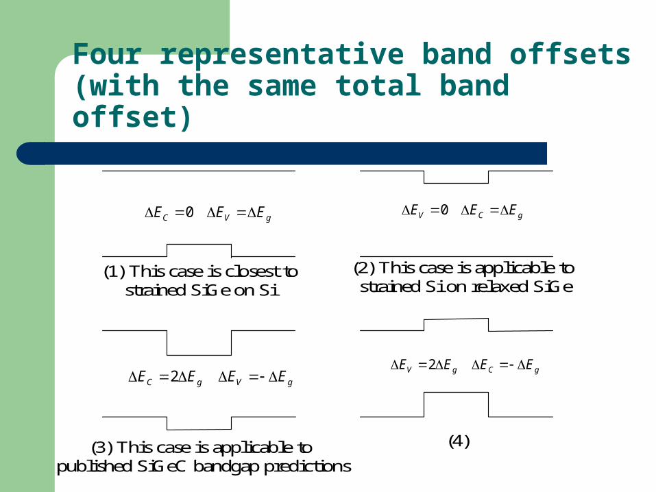
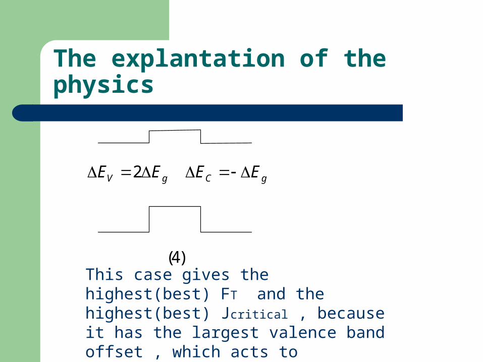
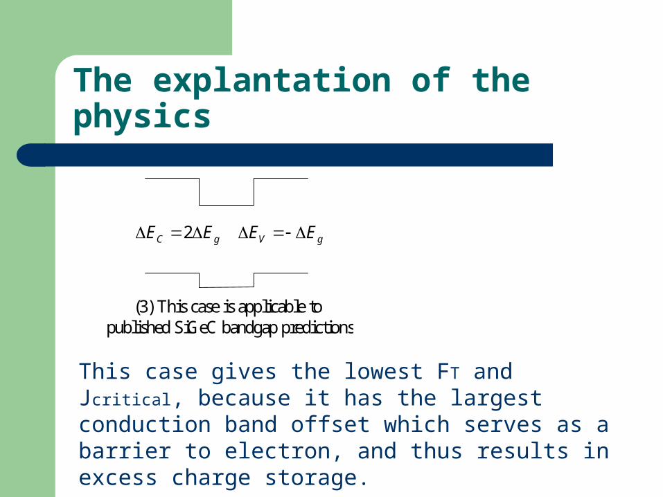
Four representative band offsets (with the same total band offset)
gVC EEE 0 gCV EEE 0
gVgC EEEE 2gCgV EEEE 2
(1) This case is closest to strained SiGe on Si
(2) This case is applicable to strained Si on relaxed SiGe
(3) This case is applicable to published SiGeC bandgap predictions
(4)
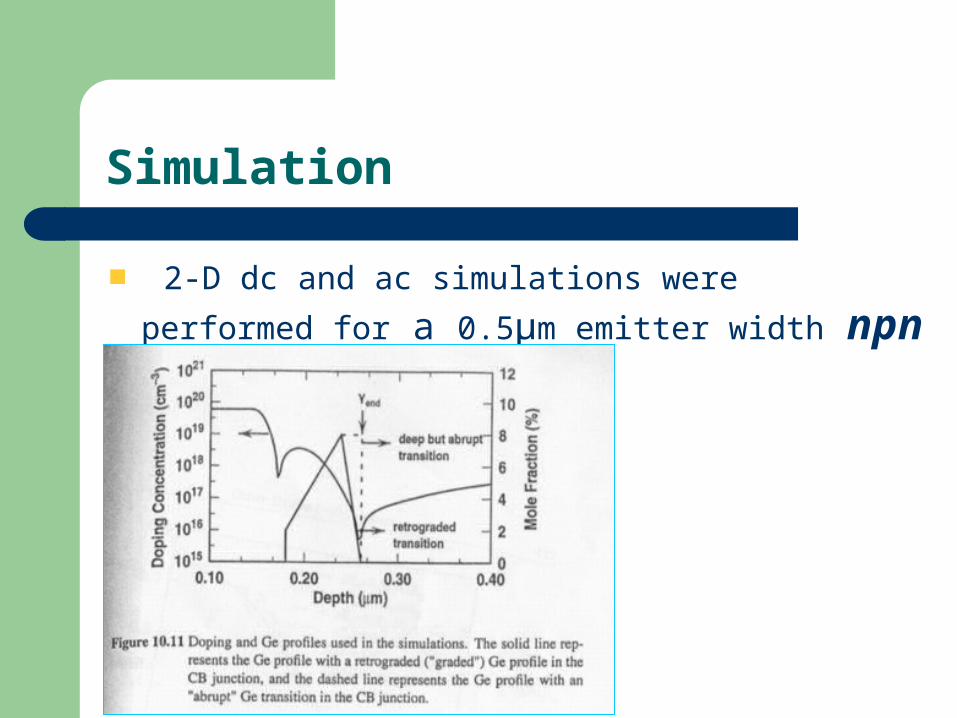
Simulation
2-D dc and ac simulations were performed for a 0.5µm emitter width npn SiGe HBT.
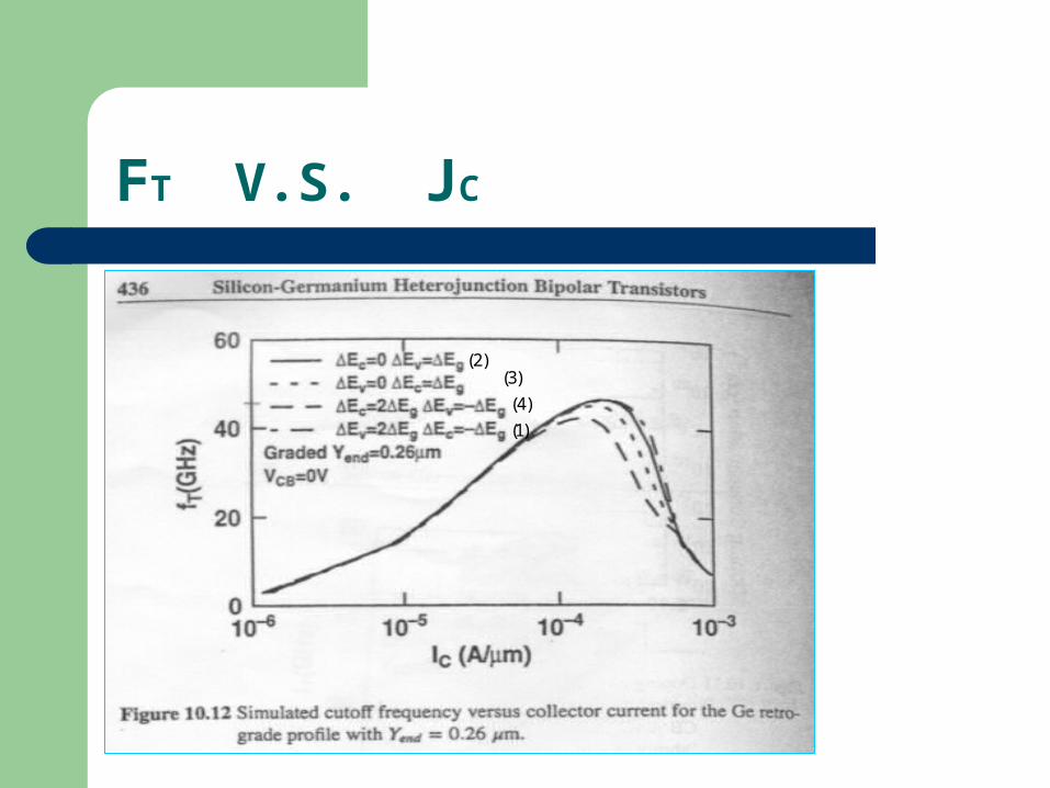
FT V.S. JC
)1(
)2()3(
)4(
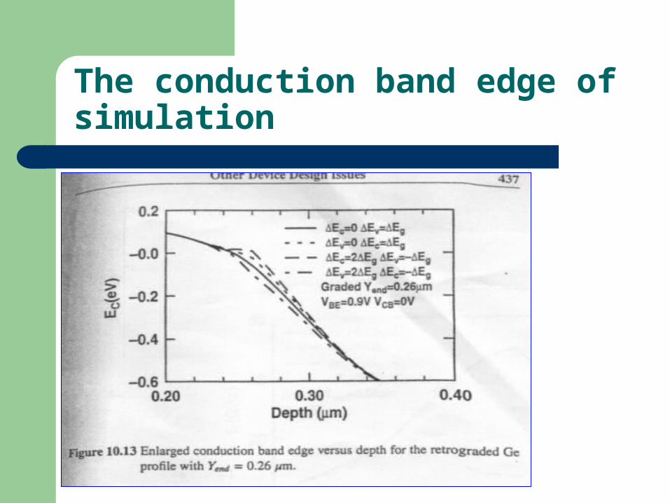
The conduction band edge of simulation
The explantation of the physics
This case gives the highest(best) FT and the highest(best) Jcritical , because it has the largest valence band offset , which acts to effectively prevent hole injection into the collector.
gCgV EEEE 2
(4)
The explantation of the physics
(3) This case is applicable to published SiGeC bandgap predictions
gVgC EEEE 2
This case gives the lowest FT and Jcritical, because it has the largest conduction band offset which serves as a barrier to electron, and thus results in excess charge storage.
The explantation of the physics
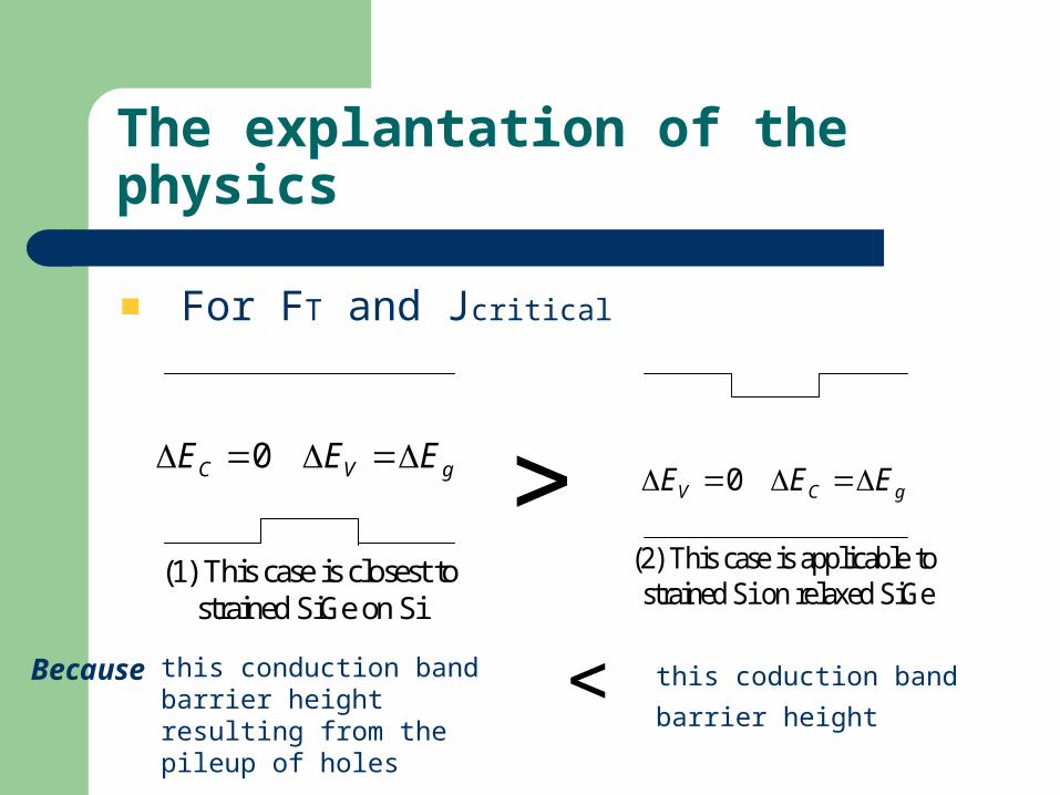
For FT and Jcritical
(1) This case is closest to strained SiGe on Si
gVC EEE 0gCV EEE 0
(2) This case is applicable to strained Si on relaxed SiGe
this coduction band barrier
height
this conduction band barrier height resulting from the pileup of holes
Because
SiGe HBTs under High –Current density operation
From the viewpoint of improving the ac characteristics of SiGe HBTs under high-current density operation, a large positive valence band offset together with a negative conduction band offset is the most desirable bandgap offset distribution.(as condition (4) ).
It is worth noting that these offsets(condition (1) ) are in fact different from those produced by strained SiGe on Si (i.e. mostly EV, with a small EC.)
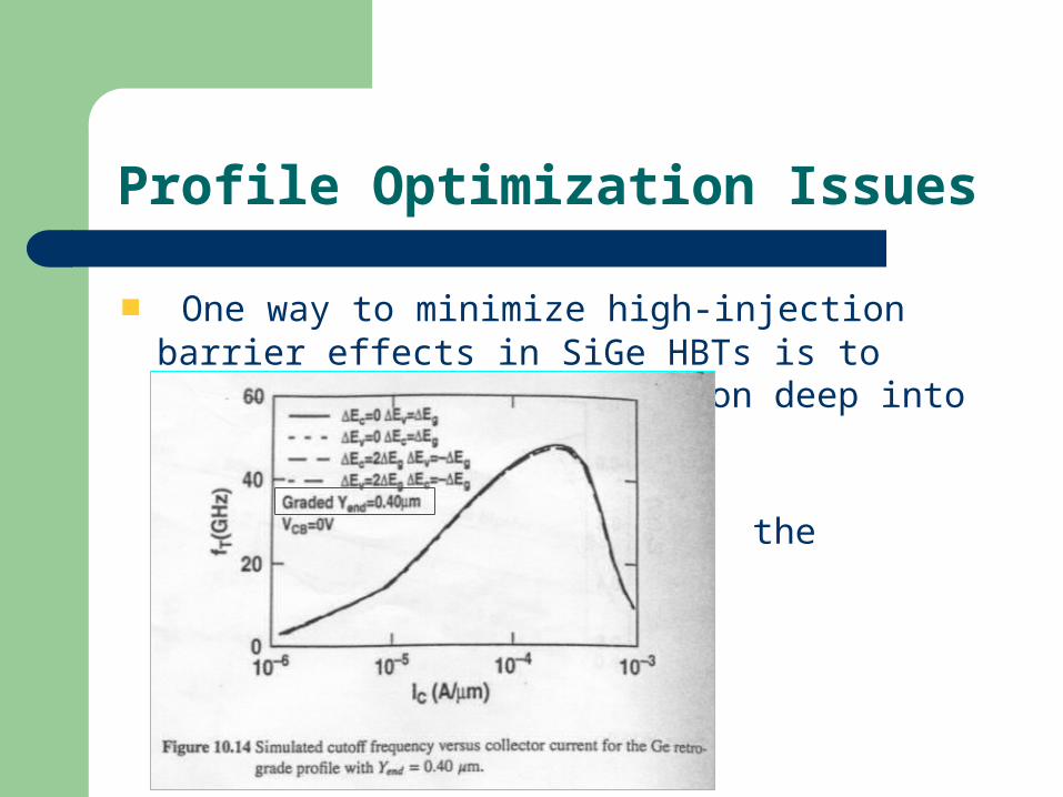
Profile Optimization Issues
One way to minimize high-injection barrier effects in SiGe HBTs is to retrograde the mole fraction deep into
the collector.
Low-C-content SiGeC
Low-C-content SiGeC layers can provide better thermodynamic stability than strained SiGe
- So we can allow a higher average Ge mole fraction for a deeper grading.
Ge-Induced Collector-Base Field Effects
The specifics of the backside Ge profile(i.e. on the CB side of the neutral base) strongly influence high-injection heterojunction barrier effects, which produce premature roll-off of and FT at high current density.
Here we will show that the backside Ge profile also alters the electric field distribution in the CB space-charge region, and thereby indirectly affects impact ionization in SiGe HBTs.
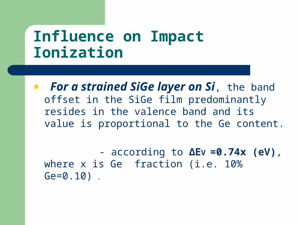
Influence on Impact Ionization
For a strained SiGe layer on Si, the band offset in the SiGe film predominantly resides in the valence band and its value is proportional to the Ge content.
- according to ΔEV =0.74x (eV), where x is Ge
fraction (i.e. 10% Ge=0.10) .
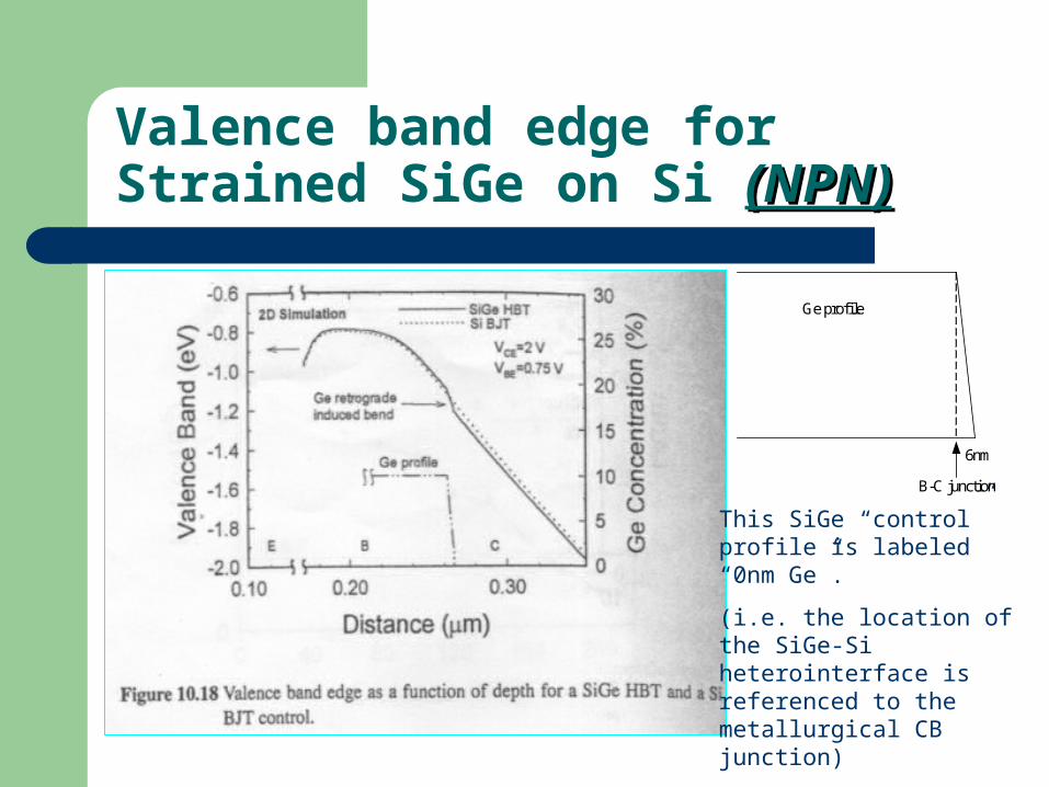
Valence band edge for Strained SiGe on Si (NPN)(NPN)
This SiGe “control” profile is labeled “0nm Ge”.
(i.e. the location of the SiGe-Si heterointerface is referenced to the metallurgical CB junction)
B-C junction
6nm
Ge profile
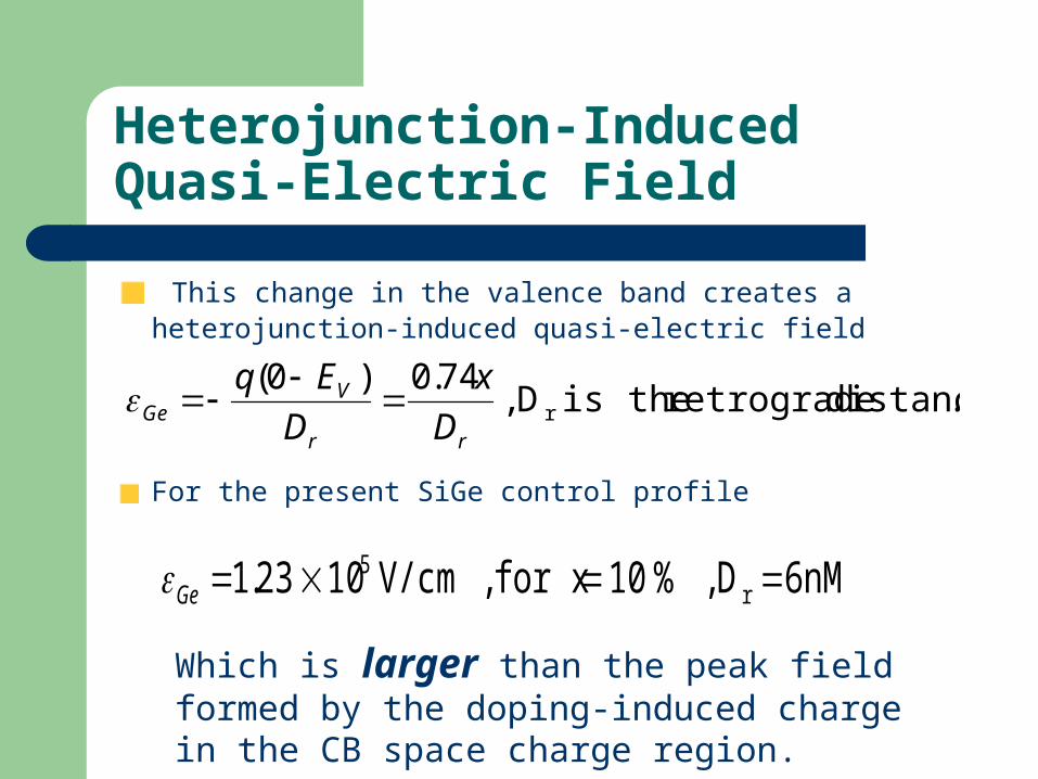
Heterojunction-Induced Quasi-Electric Field
This change in the valence band creates a heterojunction-induced quasi-electric field
For the present SiGe control profile
. distance retrograde theis D , 74.0)0(
rrr
VGe D
x
D
Eq
6nMD , % 10 for x , V/cm 10 23.1 r5 Ge
Which is larger than the peak field formed by the doping-induced charge in the CB space charge region.
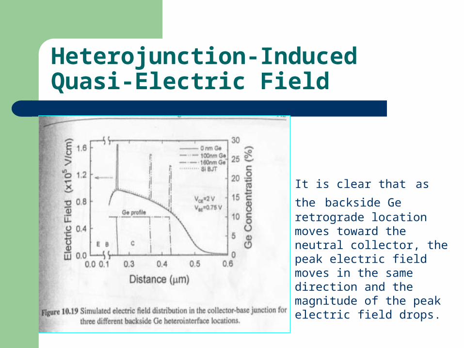
Heterojunction-Induced Quasi-Electric Field
It is clear that as the backside Ge retrograde location moves toward the neutral collector, the peak electric field moves in the same direction and the magnitude of the peak electric field drops.
絕對
值
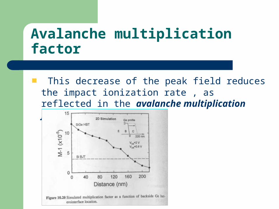
Avalanche multiplication factor
This decrease of the peak field reduces the impact ionization rate , as reflected in the avalanche multiplication factor (M-1) .