Embed Size (px)
Citation preview

1
JULY 2021 Volume IX, Issue I
RV COLLEGE OF ENGINEERING® (Autonomous Institution affiliated to VTU, Belagavi)
DEPARTMENT OF ELECTRONICS AND TELECOMMUNICATION ENGINEERING
R.V. Vidyaniketan Post, 8th Mile, Mysuru Road, BENGALURU– 560059, KARNATAKA, INDIA.
SPECIAL POINTS OF INTEREST
The Editorial Committee
The Editorial
About the Department
Nano-arbiters in the World of QCA
Scaling High-Capacity Optical Networks
Unstructured Data Storage Function in 5G
Core
Future of Quantum Computing with help of
VLSI
5G Wireless Future begins with Optical Fiber
CMOS Image Sensor: The Future of Machine
Vision Cameras
SDN Programmable IP/Optical Interworking
Machine Learning approaches in Radar Signal
Processing
WTISD - 2020 Celebrations
Institutional Activities
Online Alumni 2020
Faculty Editors: Dr. K. Sreelakshmi Prof & HoD, ETE Dr. Roja Reddy B. Associate Professor Dr. Premannad B.S. Associate Professor Prof. Viswavardhan Reddy K. Assistant Professor Student Editors:
Nikhil K, J., 1RV17TE027 VIII Sem, UG Mukul Tripathi, 1RV18TE025 VI Sem, UG Keshika Rudraganadev, 1RV20LDC10 II Sem, M.Tech DCE. Namrathaprakash, 1RV20LRF10 II Sem, M.Tech in RF & MWE
THE EDITORIAL World Telecommunication and Information Society Day (WTISD) has been celebrated annually every 17 May since 1969 to mark the founding of International Telecommuni-cation Union (ITU) and the signing of the first International Telegraph Convention in 1865. The COVID-19 crisis has not only highlighted the critical role of information and communication technologies (ICTs) for continued functioning of societies but has also brought to the fore the startling digital inequalities between and within countries. ITU Members have stepped up and engaged in activities that have proven essential in saving lives and sustaining economies. They have demonstrated their remarkable resilience in the face of challenging times. At the same time, the COVID-19 pandemic has highlighted the urgency of accelerating digital transformation and advancing the goals and targets of the Connect 2030 Agenda to leave no one behind.
WTISD 2021 is an opportunity for ITU membership to continue to push for digital transformation by promoting national strate-gies on ICT development, smart policies to encourage investments, cooperation, and partnership. ITU invites you to actively par-ticipate in commemorating the theme of WTISD 2021, "Accelerating Digital Trans-formation in challenging times", throughout the year with national, regional, and interna-tional initiatives to accelerate digital transfor-mation as highlighted.
1. Raise awareness of this year's theme, “Accelerating Digital Transformation in chal-lenging times”.
2. Reflect how ITU and its membership re-spond and adapt to new challenges through ICTs.
3. Enhance cooperation between govern-ments, business communities, UN bodies, civil society and other stakeholders in challenging times.
4. Reinforce the importance of developing digital strategies and other technology-driven initiatives as part of digi-tal transformation.
5. Consider both the opportunities and/or challenges of digital transformation when trying to find timely and effective answers to the different challenges that the world may experience.
6. Share with ITU their challenges, lessons learned, expertise, guidelines, success sto-ries, case studies, good practices, solu-tions, publications, and policies put in place to better meet future challenging times. Source: www.un.org/sustainabledevelopment/sustainable-development-goals
Since 2003
2
ABOUT THE DEPARTMENT
Department of Electronics and Telecommunication Engineering started in the year 1992 – 93 with one Under Graduate program, two Post Graduate programs. Moreover the depart-ment is recognized as a research center under VTU to carry out M.Sc. (Eng..) and Ph. D.
U.G Program: Bachelor of Engineering in Electronics and Telecommunication Engineering with an intake of 60 under gone multiple cycles of Accreditation.
P.G Programs: Master of Technology in Digital Communication Engineering with intake of 36, accredited by National Board of Accreditation, New Delhi. Master of Technology in RF & Microwave Engineering with intake of 18, accredited by NBA, New Delhi. The department has a total of 22 teaching faculty members, out of which 10 are Ph. D hold-
ers, 12 are pursuing PhD and competent technical and support staff.
Department developed industry based labs such as Keysight (Advanced RF and Wireless Communication Lab), Tejas networks Lab to strengthen U.G, P.G. projects and Research activities. The details of the research labs are listed as follows: 1) RVCE-Keysight Advanced RF and Wireless Research Lab:
2) RVCE-Tejas Optical Research Lab:
Ph. D Awarded:
FACILITIES AVAILABLE
Agilent Vector Signal Analyzer: EXA 26.5
GHz:
20 PC Workstations loaded with Agilent
EDA Tools
Agilent MIMO Baseband Generator PXB
Agilent Mixed Signal Oscilloscope,4 Ch, 4
GSa/s with 16 Digital Channels
Agilent Vector Signal Generator
TECHNOLOGIES SUPPORTED
GSM/GPRS/EGPRS
WCDMA/HSDPA/HSUPA/HSPA+
AMPS/IS95A-B/IS2000/EVDOA-B
WLAN/BT/ZigBee/RFID/WiMax/LTE
MIMO
DC-HSDPA
SDR, Cognitive Radio
FACILITIES AVAILABLE
Tejas 1600C SDH Optical Transport
equipment
Tejas 3301 CWDM Equipment with
ROADM facility
RXT2380RxT2.5G Test set up
RXT2380 SW 25G Test set up
TECHNOLOGIES SUPPORTED
SONET
SDH
CDWM
DWDM
Packet transport
Programs Offered
Research Facilities
Department Activities
Workshops/Conference Organized
One Week Online Hands-on Work-
shop on “5G NEW RADIO” Under the IEEE RVCE Signal Processing Stu-dent Chapter in association with Ca-dence Design Stystems, Mathworks and Keysight Technologies from 14th to 19th September 2020.
One Week Online Workshop on
“Signal Processing and Applications” Under the IEEE RVCE Signal Pro-cessing Student Chapter Hands-On from CoreEL Technologies (l) Private Limited and RVCE from 1st to 6th
February 2021.
One week Workshop conducted for
Technical staff on Basics of MATLAB & LABVIEW for Engineering Appli-cations-Phase-1 Jointly Organized by Dept of ETE and IEEE-RVCE-SPS student Chapter, RVCE on Feb 1 to 5th 2021.
One Week Online Workshop on
“Modern antennas for Wireless com-munication systems” Jointly Orga-nized by Dept of ETE and IEEE-RVCE-APS student Chapter, RVCE, on 5th to 10th July 2021.
Invited talks delivered by faculty:
Dr. G. Sadashivappa on “Faculty
development program on Blumes taxonomy and CIE, SEE question paper taxonomy” at Rajarajeshwari
College of Engineering, Bengaluru on 20/01/2020.
Dr. G. Sadashivappa on “Faculty
development program on outcome based technology and NBA ” at Raja-rajeshwari College of Engineering,
Bengaluru on 23/01/2020.
Dr. G. Sadashivappa on “Artificial
Intelligence in wireless communica-
tion” at SSIT, Tumkur on 12/02/2020.
Dr. H.V. Kumaraswamy on
“Communication Technologies” at Dept of ET Jyothi Institute of Technol-ogy on 05/02/2020 .
Sri.P Nagaraju on “Overview of vari-
ous Domains for ECEngineers and career opportunities” at Dept of ET Jyothi Institute of Technology on 20/02/2020 .
Dr. Nagamani K. on “ Impact of IoT at
present and in future Prospects ” at Govt. College of Engineering Rama-nagara on 10/07/2021.
Dr. R Bhagya on “Data analytics
using AI & ML”, at HKBK College of Engineering, on 17/04/2021.
Dr. R Bhagya on “Computer vision
techniques in AI & ML”, during one month internship on AI & ML, organ-ised by IETE, Bengaluru from 31/09/2020 to 26/ 09/2020.
Prof. Ushapadma on “Quality Through
Accreditation” at HKBK College of Engineering, on 17.02.21.
Prof.. Ushapadma om “ Routing using
CISCO Packet Tracer” at HKBK College of Engineering, on 17.04.21.
Sl. No.
Name of the Research Scholar
Topic
1 RAMAVENKATESWARAN NAGARAJAN USN : 1RV11PEN05
Study of low temperature grown nano cluster carbon based thin film transistor
2 DEEPTHIMURTHY T S USN : 1RV12PEN07
Study and Investigation Of Computer Aided Diagnosis Tool For Detection Of Brain Tumor
3 RANJANI G USN : 1RV12PEN14
Comparative analysis and modeling of underwater acoustic channel
4 BHARTHI GURURAJ USN : 1RV12PEN15
Study and Investigation on Error-resilient wireless image transmission using packetization and channel coding
5 NAGARAJA P USN : 1RV13PEN15
Fault Diagnosis of Hybrid Circuits Using Statistical Proper-ties Based on Classifiers and Implementation Using SVM

3
Outside Interaction :
Dr. G. Sadashivappa, Mem-ber-Expert for BoS - ECE Dept., GAT Bengaluru.
Dr. K. Nagamani, “Judge in the Ideathon” during the Induction Programme for First year students RVCE on 6 Jan. 2020.
Dr. Bhagya R Member of ‘Editorial Board’ of ‘Lattice Science Publication’ and it’s journal (s) for year 2020-21.
BoE in other Institutions:
Dr. H.V. Kumaraswamy, MSRIT, ETE Dept.
Prof. P. Nagaraju, Dr. AIT, ECE Dept.
Dr Nagamani K., MSRIT, ECE Dept.
Dr. Premananda B.S., MSRIT, ECE Dept.
Dr. B. Roja Reddy, Dr. AIT, ETE Dept.
Ph. D. Doctoral committee Member in other Institutions:
Dr. G. Sadashivappa
Dr. K. Sreelakshmi
Dr. H.V. Kumaraswmay
Dr. Nagamani K.
Dr. Premananda B.S.
Senior IEEE Members:
Dr. K Sreelakshmi
Dr Nagamani K.
Dr. B. Roja Reddy
Dr. Premananda B.S.
Dr. Shanthi P.
ABOUT THE DEPARTMENT….
Faculty Membership of Professional Bodies
U.G. Rank Holders (2016-2020 Batch):
P.G. Rank Holders (2018-2020 Batch) :
M.Tech in Digital Communication Engineering
M.Tech in RF and Microwave Engineering
Faculty/Student Publica-tions:
Publication from July-2020 to July-2021
1) International Journal: 23
2) International Conference: 32
Sl. No. Faculty Name Association Membership Detail
1 DR. K. SREELAKSHMI IEEE/IETE MTT & AP Societies No: 93879876 / M 144426
2 DR. H.V. KUMARASWAMY IEEE/IETE No: 97518487 / F131347
3 PROF. P. NAGARAJU IEEE/IETE No: 97518449 / F131353
4 DR. K NAGAMANI IEEE Signal Processing Societies No: 94839025
5 DR. R BHAGYA IEEE No: 95663275
6 DR. B. ROJA REDDY IEEE/IETE No: 94817651 / F 230094
7 DR. PREMANANDA B. S. IEEE No. 92328975
8 DR. K. SARASWATHI IEEE No. 92375938
9 DR. SHANTHI A. IEEE No: 95654327
10 PROF. MOHANA IEEE No: 95188416
11 PROF. K. VISWAVARDHAN REDDY IEEE No. 90514368
12 DR. RANJANI G IEEE / IETE No: 96931775 / AM 191965
Sl. No.
USN Name of the Student Rank CGPA
1 1RV16TE022 KRISHNA C. V I 9.60
2 1RV16TE057 VAISHNAVI S. PARASHAR II 9.50
3 1RV16TE044 SHREESHA YERRAGOLLA III 9.22
4 1RV16TE017 HARSHITHA S IV 9.18
5 1RV16TE012 DHANUSH T. N V 8.84
6 1RV16TE032 POORVIKA R VI 8.83
Sl. No.
USN Name of the Student Rank CGPA
1 1RV18LDC16 NAGALAKSHMI PRANITHA S I 9.67
2 1RV18LDC20 POOJA DAYANANDA K I 9.67
3 1RV18LDC05 BHAVANA GANGA R II 9.53
4 1RV18LDC14 MEGHANA S III 9.31
Sl. No.
USN Name of the student Rank CGPA
1 1RV18LRF05 MISBA FATIMA I 9.07
2 1RV18LRF07 PRAKRUTHI M II 8.80
3 1RV18LRF10 PRIYANKA P. N. III 8.73
4
Quantum-dot Cellular Automata (QCA) is a revolutionary computing paradigm that is well suited to nano-electronic implementation and scaling to molecular dimensions. In QCA, binary information is encoded in the position of single electrons among a group of dots forming a cell. Electrons switch between quantum dots within a cell, but no current flows between cells. This leads to extremely low energy dissipation, avoiding the problem of heat generation that ultimately limits the integration density of transistor circuits. Developments in the field of quantum computing have been strongly impacted by the paradigm of QCA.
Arbiters are the essential components of the Network-On-Chip (NOC) systems and are used to resolve the contention problem where multiple requests must be handled for shared re-sources. With an ever increasing pace in the development of fast and compact chips in the semiconductor market, the number of integrated cores in a single chip has dramatically in-creased. This trend inevitably leads to new paradigms in the fabrication, interconnections, and integration processes. An example is the System on Chip (SOC) where the scales of a multi-component system are supposed to be miniaturized at chip scales. Interconnections provided in large scales are swapped with various physical and technical restrictions. One such restriction arises in interconnecting core components in the SOC designs. As a result, ideas from computer networking have been put forward as a solution for the drawbacks in the traditional interconnections strategies. This has led to the NOC design schema as a promising candidate for handling the interconnection problem in SOCs. NOC designs main-ly consist of a network of routers (nodes) that are connected to each other by some commu-nication links with the advantage of being more scalable and reliable.
In a NOC design, the router is the main building block, which is supposed to receive packets from the source, and then according to a routing strategy and network topology transmits packets to its immediately attached core or other routers. In addition, the routers determine the overall strategy for moving data throughout the whole NOC perimeter and perform the flow control policies (routing, arbitrating, etc.). Generally, an arbiter is the main element in shared resource systems such as routers that are usually placed where the major bottleneck for the throughput exists. It must preserve a fair arbitration in response to the received re-quests and consumes less power in a minimum area. Hence, the delay, the layout area, and the power consumption are the candidate benchmarks for the evaluation of arbiters.
A dedicated arbitration circuit (or arbiter) is used to provide access to one or more shared resources, such as memory, difficult data processors or channels of communication. The main task of an arbiter is the scheduling and prioritization between input requests for shared resources. A fundamental illustration of an arbitration process: suppose two transmitters that require sending data over a common network connection (channel). They cannot use the channel at the same time, so they are requesting a dedicated arbiter to approve access to the shared resource. The arbiter in turn ensures that the resource is available before access is granted to any of them.
The first part is a programmable arbitration logic that decides which requests are granted according to the current state of the priority vector. The second part is the pointer update logic that decides which of the requests in the next cycle will be prioritized according to the current grant vector. Given the expected role of an arbiter in NOCs, various designs have been proposed based on the conventional transistor technology. However, with the ever in-creasing downsizing trend in the fabrication technology, the frontier of this trend has now touched nano-scales. In those scales, the size, the power consumption, and the interconnec-tion facilities are among the most intriguing challenges confronted by design strategies such as those paradigms (QCA) that offer a higher fabrication density, lesser power consumption, and more flexibility in interconnections down to atomic and molecular scales. Hence, QCA with its nano scales and very low power consumption is a promising candidate for imple-menting future NOCs.
Therefore, NoC is a solution for various constraints encountered in miniaturized SOCs, es-pecially in nano-scales. QCA is a nano-scale proposal with the potential for the realization of a few arbiters’ architectures as the main component of the routers in NOCs. It can be not-ed that arbiters with more inputs along with other factors (such as fair arbitration) might affect the performance of an arbiter. Arbiters also serve as basic building blocks in asyn-chronous computational systems.
Nikhil K.J. (VIII Sem), Dr. Premananda B.S.
The coronavirus COVID-19 is affecting :
212 countries
and territories
around the world and 2 interna-tional conveyances
Statistics can be found in the below link:
https://www.worldometers.info/coronavirus/
Nano-arbiters in the world of QCA
5
Placement statistics for VIII Semester BE Tele-communication students:
Number of eligible stu-dents : 58
Number of offers made: 66
Number of students placed: 40
Number of students with open dream package: 19
Number of students with dream package: 25
Placement statistics for PG DCE students:
Placed IV sem DCE: 10
Internship: 17
Placed IV RF&MWE: 03
Internships: 06
Scaling High-Capacity Optical Networks
The approach of high-bandwidth over-the-top (OTT) services, the growth of broadband and mobile data in developing markets and the development of expansive web-based web compa-nies such as Google, Amazon and Facebook are creating a disruptive impact on the wholesale bandwidth industry. In recent years, Alien Wave technology has emerged as a popular, technologi-cally mature and cost-effective method to rapidly upgrade capacities on “brownfield” DWDM (Dense Wavelength Division Multiplexing) net-works without having to invest in a new capital-intensive network. One recent development in the DWDM space which has captured global market attention is Alien Wavelength (AW) transport. A practical example of an AW implementation is one where network resources owned by one carri-er are being utilised to transport optical channels that are in the control of a secondary carrier. The possibility of AW insertion without any impact to existing services has resulted in a rapid acceptance of this technology by the telecom service provider community. AW technology is a coherent technology that utilizes phase-shift keying and can support 100G rate.. The power density difference in traditional 10G channels over 100G channels cause them to have greater impact on refractive index (RI) of the transmission media. The changing RI alters the phase of the wavelengths traversing through the transmission media, both of itself (nonlinear effect known as Self Phase Modulation (SPM)) as well as of other wavelengths (nonlinear effect known as Cross Phase Modulation (XPM)). Since coherent technology based 100G channels use phase encoding to transmit user data, they are adversely impacted by phase anomalies. This in turn leads to degraded channel performance both in terms of transmission reach as well as the ability to guarantee error-free transmission. Also, low values of residual dispersion amplify the probability of XPM on 100G. AW technology represents a significant advantage to expand capacity on existing DWDM networks and has several advantages for telecom service providers. Alien Wavelength (AW) technology has emerged as a cost-effective option to progressively scale bandwidth in DWDM networks. It extends network lifetime by being able to support different modulation formats on a common optical infrastruc-ture. AW technology encourages reuse and sharing of a network and avoids duplication of network builds thus reducing total capital expenditure.
Kiran Prabhakar, II semester M.Tech (DCE), Dr. Ranjani G
Unstructured Data Storage Function in 5G Core
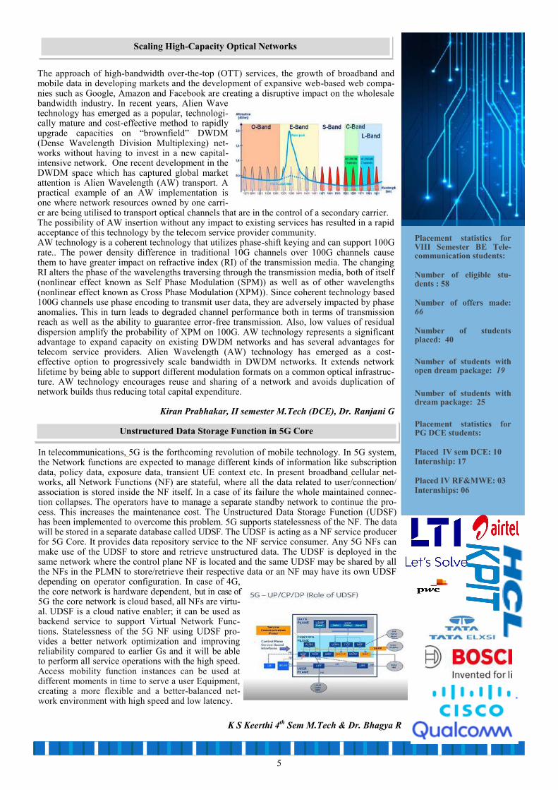
In telecommunications, 5G is the forthcoming revolution of mobile technology. In 5G system, the Network functions are expected to manage different kinds of information like subscription data, policy data, exposure data, transient UE context etc. In present broadband cellular net-works, all Network Functions (NF) are stateful, where all the data related to user/connection/association is stored inside the NF itself. In a case of its failure the whole maintained connec-tion collapses. The operators have to manage a separate standby network to continue the pro-cess. This increases the maintenance cost. The Unstructured Data Storage Function (UDSF) has been implemented to overcome this problem. 5G supports statelessness of the NF. The data will be stored in a separate database called UDSF. The UDSF is acting as a NF service producer for 5G Core. It provides data repository service to the NF service consumer. Any 5G NFs can make use of the UDSF to store and retrieve unstructured data. The UDSF is deployed in the same network where the control plane NF is located and the same UDSF may be shared by all the NFs in the PLMN to store/retrieve their respective data or an NF may have its own UDSF depending on operator configuration. In case of 4G, the core network is hardware dependent, but in case of 5G the core network is cloud based, all NFs are virtu-al. UDSF is a cloud native enabler; it can be used as backend service to support Virtual Network Func-tions. Statelessness of the 5G NF using UDSF pro-vides a better network optimization and improving reliability compared to earlier Gs and it will be able to perform all service operations with the high speed. Access mobility function instances can be used at different moments in time to serve a user Equipment, creating a more flexible and a better-balanced net-work environment with high speed and low latency.
K S Keerthi 4th Sem M.Tech & Dr. Bhagya R

6
The Future of the communication is of wireless which is fixed. 5G mobile technology is going to be the best technology in the history of the mobile technology. But without optical fiber supporting the 5G will not be best technology. The technical reasons for why 5G requires the optical fiber for the low-latency, high-bandwidth traffic. Firstly, there is a simple fact that better communications increase GDP. The regions benefiting the most from wireless com-munication have the best fixed access networks. In the recent years of the communication technology, the return has been driving M&A activity between mobile –only and fixed-only operators.
High Fiber availability = faster 5G deployment = faster time to market There are only two backhaul technologies that can cope with high-throughput and low-latency demands of 5G: microwave and optical fiber. The early announcements are primarily coming from the operators in countries who has the high optical fiber availability. Everyone else should come up with some of the innovative idea on optical fiber investment strategies, if 5G is going to continue in the country. A recent FTTH (fiber-to-the-home) Council Europe study claims that where the FTTH, the incremental cost to make the network 5G-ready are marginal: you virtually get the 5G network for free. Similar Fiber/5G symbiosis can be found in Singapore, South Korea, Hong Kong, New Zealand and Qatar. The Economics of optical fiber infrastructure tells that to use the full potential of 5G’s we need the concerted socio-political effort along with the mar-ket forces.
Ajay C. N., II semester M.Tech (DCE), Dr. Ranjani G.
A 5G Wireless Future begins with Optical Fiber
Future of Quantum Computing with help of VLSI
Quantum Computing (QC) is a computational paradigm where Quantum Mechanics (QM) is utilized for encoding information and doing calculations just like normal computers. These computers can be made sophisticated and efficient by using the latest VLSI technologies. Quantum computers can be controlled by looking into all the possible solutions for an existing problem. The initial state is known, and there is a limited set of basic elements which is known as qubits that can be manipulated by a simple set of rules rotations of the vector that represents the quantum state. The first commercial quantum computer was built by IBM, this com-puter comprises 53 qubits and is fully functional via cloud networks. The materials required for building qubits are made from supercon-ductor metals. The lower temperature problem of QC can be tackled by using VLSI with CMOS technology in this regard INTEL in alli-ance with QuTech have made quantum chips which can perform cal-culations at 3K. The quantum chip made is called the Horse Ridge. It is a cryogenic control chip that can be used for making QC slimmer, faster and more efficient in regards to temperature with less use of coolants. The chip is fabricated using Intel’s 22nm FinFET low power technology (22FFL). It is designed for radio frequency processors to control qubits operations. The chip is capable of handling a wide range of frequencies between 14 to 20GHz and superconducting qubits at range of 6 to 7GHz. The chips that work at lower temperatures are termed cryo chips and hence CMOS technologies can be used for fabrication using the principle of fault tolerant loops. A qubit is a quantum dot where an electron is confined and Quantum point contact to sense the spin of the electron by measuring the cur-rent flowing from source to drain. The QPC known as Quantum point contact is a revised RC circuit which consists of I to V converter, LPF and ADC. A DAC converter can be used to generate appropriate voltage. This concept can be used to make multi-qubit systems, where the circles at the lower level represent three quantum dots cou-pled through quantum tunnelling barriers. The implementation of CMOS multiplexers at base temperature (20mK) and the removal of SQD (sensing quantum dot) that senses charges in the quantum dots by means of dispersive readout techniques could accelerate the crea-tion of large-scale classical-quantum interfaces. In a generic system for a scalable qubit array where the majority of the components of the system are operating at 4.5K temperature, the circuit performs local error correction, readout, and drives execution. Radio-frequency signals may be generated locally. The FPGA used for fabrication of a 28-nm CMOS chip performs well with performance parameters better when compared to that at temperature. We can conclude that compared to other fabrication techniques CMOS transistors are suitable for implementing multiplexing functions and more complex circuitry at even lower temperatures that can be useful for quantum computation. Skanda C. (VI Sem), Dr. Premananda B.S.

7
In recent days, the market for solid state image sensors has been experiencing exponential growth due to increased demands of mobile imaging, internet based video conferencing, surveillance and biometrics. In other words image sensors have become a significant and dominant silicon technology driver. The different image sensors used in digital cameras and modern phones are Charged Coupled Devices (CCDs) and CMOS. CCDs have been the dominant image sensor technology, but recent advancements in technology in the field of image sensors have evolved and currently CMOS image sensors have proven to be a viable alterna-tive to CCDs. CMOS image sensors offer many advantages when compared to CCDs such as low voltage operation, low power consumption, on chip functionality and lower cost. By exploiting the ability to integrate sensing with analog and digital pro-cessing down to the pixel level, new types of CMOS imaging devices are being created for machine vision, man-machine inter-face, surveillance and monitoring. The different forms of CMOS image sensors are passive CMOS sensors and active pixel CMOS image sensors. Passive CMOS image sensors are used in applications such as low cost and low performance. In passive CMOS sensors the pho-todiodes are arranged in the form of an array with each photodiode connected to a switch which is in turn connected to a vertical output line. The vertical output line is connected to a horizontal output line which will be connected to an amplifier and will be subjected to further processing. With the combination of switches it is possible to connect any photodiode to the output amplifier. It is important to understand that switches are basically MOS transistors. But the disadvantage of a passive image sensor is that it provides poor performance and high noise. The limitations of passive CMOS image sensors can be overcome by using three transistors per pixel and this type of configuration is known as active CMOS image sensor. The transistor ( Msf ) shown in Fig. acts as an amplifier, this enables the image sensor to drive a voltage from each pixel instead of a charge packet which is far more efficient and also gives higher speed and better noise performance. The transistor ( Mrst ) serves as a reset transistor for the photo diode. The third transistor (Msel ) is used as a row select transistor which is identical to what is used in passive CMOS sensors. The row and column select lines are connected to an amplifier for further processing. But in an active CMOS image sensor each row is expressed at a time slightly greater than the previous row, this phenomenon gives rise to rolling shutter. Roll-ing shutter causes the image of the moving object to have a skew distor-tion. So this effect can be removed by having a global shutter. The CMOS image sensor market was valued at USD 7.21 Billion in 2013 and in 2020 the worth was increased to USD 10.17 Billion. Also MNCs like Sony invested USD 805 million to increase the CMOS image sensor production in 2015. According to some recent research reports, the CMOS image sensor market has various segments in the field of technology, specification, visible and non-visible spectrum and applications in Aerospace, automotive, healthcare and consumer electronics.
Srivatsa B. (VI Sem), Dr. Premananda B.S.
CMOS Image Sensor: The Future of Machine Vision Cameras
SDN Programmable IP/Optical Interworking
The digital era of 5G and the cloud triggers a new cycle of network investments and presents key opportunity for operators to reflect and reassess the present network and determine what improvements or changes are needed for the future. The evolution and interworking of IP routing and optical transport is a critical success factor for many operators because it greatly determines the quality, reliability and cost-efficiency of their network and the services it delivers. Multi-layer carrier SDN allows operating a converged network fabric with visibility and control over both IP and optical domains to overcome the issues of siloed manage-ment approaches. A multi-layer topology view can be created by discovering and correlating multi-layer connectivity through Link Layer Discov-ery Protocol snooping or by comparing traffic counts on ports.The Nokia NSP addresses these needs with a multi-vendor carrier SDN solution to help network operators build and operate an agile, programmable and cost-efficient IP/optical network fabric that meets the new service delivery challenges of the digital era.

8
Shruthi S, II semester M.Tech (DCE), Dr. Ranjani G.
The radar community has started applying Machine Learning (ML)-based algorithms to classic and new radar research do-mains to tackle traditional and new challenges from a novel prospective. Few areas where ML based algorithms applicable are Radar Radiation Sources Classification and Recognition (RRSCR), Anti-jamming and interference mitigation, Waveform Optimal Design, Cognitive Electronics Warfare, Antenna Array Design, Radar Spectrum Allocation, Moving Target Indica-tor, End to End unified Intelligent detective architecture, Target detection and tracking intelligent unified processing, End to End framework of unified detection, tracking and Recognition. Radar Radiation Sources Classification and Recognition: The increasingly growing complexity of electromagnetic envi-ronment demonstrates severe challenges for RRSCR, such as the increasingly violent electronic confrontation and the emer-gence of new types of radar signals generally degrade the recognition performance of statistic modeling techniques, especial-ly at low signal noise ratio (SNR) scenario. End-to-End Unified Intelligent Detection Architecture: The outputs of neural network withcross entropy as loss function satisfied the Neyman-Pearson detection criterion. Therefore, it is promising to exploit an intelligent end-to-end architecture by taking full use of the general non-linear fitting ability for radar target detection. The challengeable research problems in-clude the intelligent constant false alarm rate, environment identification (such as noise and clutter background automatic classification) techniques. Target Detection and Tracking-Unified Intelligent Processing: It is possible to optimally adjust the detec-tion threshold via prior knowledge-based online learn-ing techniques, which is based on the feedback from target tracking information (such as motion trends, co-variance estimation) to target detection units. End-to-End Framework of Unified Target Detec-tion, Tracking and Recognition: To achieve unified intelligent processing for clutter suppression, radar target detection, tracking, and recognition by Artificial Neural Networks (ANNs_-based multi-task learning. Because of powerful non-linear fitting ability, ANNs have high performance in classification and recognition tasks. According to the targets (valuable targets, clutter or noise background) recognition information, radar (Courtesy : www.electronicdesign.com)
can program the optimal tracking route based on the ANNs-based prediction of target flight trajectory. There is a strong evi-dence of the extensive development of ML-based Radar Signal Processing (RSP) algorithms that have found application in several radar-related fields many researchers have begun to apply radar signals as inputs to various deep learning networks for object detection, object segmentation, object classification and their combination with vision data for deep-learning-based multi-modal object detection . The range and the velocity estimation of different kinds of radar systems, such as Frequency Modulated Continuous Wave (FMCW), Frequency Shift Keying (FSK), and Multiple Frequency Shift Keying (MFSK) waveforms commonly employed in automotive radars. Radar waveform optimization design, radar spectrum allocation, Cognitive radar detection, antenna array selection, and Mov-ing Target Indication (MTI) using CNN are research fields where ML are applied. SAR imagery processing methodologies includes denoising, classification and recognition, detection and segmentation. In recent years, with the rapid development of ML in image processing, ML-based, has applied to SAR image processing widely and successfully. Artificial Inteligence can also replace human operators in systems where human involvement is required for target recognition. Automatic learning of
radar waveforms, feature extraction, identification is required to use in artificial intelligence Systems. Dr. B. Roja Reddy
Machine Learning approaches in Radar Signal Processing

9
To mark the celebrations of “World Telecommunication and Information Society Day –WTISD-2020” a webinar and one session on paper presentation organized on 18th May 2020, by Department of Telecommunication Engineering, RV Col-lege of Engineering, Bengaluru. This year’s theme released by ITU was “Connect 2030: ICTs for the Sustainable Develop-ment Goals (SDGs)”. Organization of the National Conference is an annual event of the institution to spread awareness, research opportunities for serving the society and enhancing technical interaction among Faculty, Researchers and Students. But this year due to the pandemic, the celebrations were limited. The celebration was sponsored by RSST, Technilab Instrument. There was realise of Tarangavani, which is department newsletter where the faculty and students articles and their achievements are published, announcement of Arunodaya Schol-arship, which is given to department UG students every year but from this year PG students are also included, one webinar and one presentation session. Celebrations of the World Telecommunication and Information Society Day: (18-05-2020). There was a formal wel-come from HOD, TCE.
Welcome address by Dr. K. Sreelakshmi Release of Tarangavani Newsletter
Principal’s Address Arunodaya Scholarship Announcement
There was a webinar by Dr. M. H. Kori on “AI, ML & Other Key Technologies driven by 5G” There was one online paper presentation session chaired by Dr. H.V. Kumaraswamy and Dr. K Nagamani. The total number of papers presented was 6 from RVCE out of which 2 are from CSE and 4 are from TCE departments. There were around 50 participants in the Audio-Video Seminar Hall and 100 online participants from various departments.
Webinar on “AI, ML & Other Key Technologies driven by 5G” by Dr. M. H. Kori
WTISD - 2020 Celebrations

10
Arunodaya Scholarship
Sl. No. USN Name of the students Semester
1 1RV17TE404 Megha G. Patil VIII
2 1RV17TE019 Kaveri Shekhargouda Patil VI
3 1RV18TE022 Laxman Chandrashekar Dixit IV
4 1RV18TE023 M. Pooja IV
UG students:
PG students:
Sl. No. USN Name of the students Semester
1 1RV18LDC29 Sudhan A.T. IV M.Tech.
DCE
2 1RV18LRF05 Misba Fathima IV M.Tech.
RFME
Institutional Activities
Telephone Exchange in the RVCE Campus
The RVCE is managing the Telephone Network including the Hardware since 1995. During 1995 the Stowger Exchange was used which was limited to around 50 lines for the whole campus. Subsequently during 1997, New System (EPABX) was brought into having a capacity of 128 Lines with all the latest features including outgoing /incoming facility over BSNL lines, call transfer, conference etc, This system was manned by a telephone operator for transfer the incoming calls to the respective Extensions. As the demand increased the system was upgraded to 256 lines of the similar configuration during 2002. During the year 2008, the institution new technology called CENTREX which was implemented by M/s.TATA Com-munications. This system eliminated the concept of telephone operator where the incoming calls were directly landing on the extensions (DID Facility). Also, the capacity of the exchange was increased to 325 lines. This was one of the finest and reliable system till date. As the technology advanced, the Service provider was not able to support this system. During the year 2021, the new system based on M/s. NEC was setup with a capacity of 512 lines with SIP Trunk facility.

11
Centre Coordinators:
Dr.Ramakanthkumar P Dr.Ramakanthkumar P Dr.Sreelakshmi KDr.Sreelakshmi K
Professor & HoD Professor & HoD Professor & HoDProfessor & HoD
Dept. CSE, RVCEDept. CSE, RVCE Dept. ETE, RVCEDept. ETE, RVCE
Faculty Involved:
Dr. Roopa J Dr. Roopa J Dept. ECE, RVCEDept. ECE, RVCE
Dr. Hemavathy Dr. Hemavathy Dept. CSE, RVCEDept. CSE, RVCE
Dr. Azra Nasreen Dr. Azra Nasreen Dept. CSE, RVCEDept. CSE, RVCE
Prof. Neethu SProf. Neethu S Dept. ETE, RVCEDept. ETE, RVCE
Vision/Mission of CCTV Research Centre: Vision/Mission of CCTV Research Centre:
An Integrated research facility to bridge the gap in knowledge, prac-An Integrated research facility to bridge the gap in knowledge, prac-
tice, protocols, testing, experiments, training, certification and exper-tice, protocols, testing, experiments, training, certification and exper-
tise in video surveillance Multitise in video surveillance Multi--stakeholder Research facility.stakeholder Research facility.
The Center for CCTV Research, located at Bengaluru’s prestig-ious RV College of Engineering, is India’s pioneering research unit in this area, created with the intention of being the catalyst to bridge the wide gap between the industry and creation & execution of hu-mongous CCTV projects in the country. The Center aims to fulfil the Gap of knowledge, Practice, Protocols, Testing, Experiments, Certi-fication, Training, Expertise etc. While being a one stop shop for all CCTV project requirements it would be also the synthesis and the coordination center for all major CCTV players in the country and beyond. The creation and operations of this Center would be a clear manifestation of this dream. The coming together of different busi-ness entities for a project is just crude distribution of work and a confident seem less consortium which this required for this purpose.
Details
Signed MoU between CCTV Re-
search Centre, RV College of
Engineering and National Fo-
rensics Science University,
Gandhinagar.
Signed MoU between CCTV Re-
search Centre RV College of
Engineering and COM-SUR,
Mumbai
The centre shall run certification courses on basics of CCTV both theory and practice for a duration of 3 weeks open to students and Faculty of RVCE. This programme comprises of theory and hands on lab sessions associated with visits to place of CCTV installations, central monitoring stations etc to get familiar with the field operations. The objective of this pro-gramme will be to generate skilled manpower for the system integrators and shall provide suitable employment opportuni-ties. The duration of this programme shall be for 4 to 6 weeks
Institutional Activities

12
Online Alumni Meet 2020
An online alumni meet was conducted on 26-Sept-2020 at 10AM, by Dept. of Electronics and Telecommunication Engineer-ing through Cisco Webex platform. Around 100 alumni had joined the meet along with alumni office bearers and faculties.
VISION
Imparting quality education in Electronics and Telecommunication Engineering through focus on Fundamentals, Re-
search and Innovation for Sustainable Development
MISSION 1. Provide comprehensive education that prepares students to contribute effectively to the profession and society in the
field of Telecommunication.
2. Create state-of-the–art infrastructure to integrate a culture of research with a focus on Telecommunication Engineering
Education
3. Encourage students to be innovators to meet local and global needs with ethical practice
4. Create an environment for faculty to carry out research and contribute in their field of specialization, leading to Center
of Excellence with focus on affordable innovation.
5. Establish a strong and wide base linkage with industries, R&D organization and academic Institutions.
DEPARTMENT OF ELECTRONICS AND TELECOMMUNICATION ENGINEERING