Embed Size (px)
Citation preview
1
The effect of Mg doping on GaN nanowires
E. Cimpoiasu1,4, E. Stern2, R. Klie3, R. A. Munden1, G. Cheng1, and M. A. Reed1
1Departments of Electrical Engineering and Applied Physics, Yale University, New Haven, CT, 06520 2Department of Biomedical Engineering, Yale University, New Haven, CT, 06520 3Brookhaven National Laboratory, Upton, NY, 11760
We present a comparison between the structural, chemical, and electrical properties of Mg-doped
GaN nanowires grown by hot-wall chemical vapor deposition using two different Mg sources,
namely, metaloorganic bis(methylcyclopentadienyl) magnesium and magnesium nitride powder.
We find that Mg from the solid nitride source is more effectively incorporated into the nanowires
while better maintaining the nanowire integrity. After Mg activation, the nanowires are partially
or fully compensated. In comparison, vapor-phase doping results in an obvious degradation of the
nanowire morphology in spite of lower Mg incorporation levels.
PACS numbers: 73.61.Ey, 73.63.Bd, 73.63.-b
4The author to whom correspondence should be addressed; email: [email protected]
2
1. Introduction
Gallium nitride is a direct bandgap semiconductor of interest for ultraviolet and blue
optoelectronics devices. This class of devices, which includes light-emitting diodes, requires very high
quality pn junctions, and, therefore, precise doping control. To date, highly controlled p-doping of GaN
has been achieved predominantly in epitaxial thin layer structures. Recently, p-type doping and pn
junctions were demonstrated in quasi one-dimensional GaN structures, such as nanowires and nanorods
[1-3]. Magnesium was the dopant of choice in these structures, and was delivered either from a solid
source, such as magnesium nitride Mg3N2 [2], or from a metaloorganic source, such as
bis(cyclopentadienyl)magnesium (Cp)2Mg [3]. All reports on the electrical characteristics of as-grown
GaN nanowires have shown that they grow unintentionally n-type, with large carrier concentrations of
1018 to 1019 cm-3 [4-6]. Thus, fairly large quantities of magnesium must be incorporated into the
nanowires to overcome the background electron concentration due to residual donors. This can be
difficult to achieve reproducibly, because less than 1% of incorporated magnesium produces acceptor
centers at room temperature due to its large activation energy of ~ 200meV [7]. Consequently, for hole
densities of 1018 cm-3 at room temperature, one has to achieve high Mg concentrations of ~ 1020 cm-3
(which are near the solubility limit for Mg [8]).
This work presents a comparison on the effect of heavy Mg-doping on the morphology, structure,
chemical profile and electrical properties of GaN nanowires grown with a hot-wall chemical vapor
deposition system. We have used two types of Mg sources: Mg3N2 powder and
bis(methylcyclopentadienyl)magnesium [(MeCp)2Mg]. The later is less common for p-type doping of III-
V alloys compared to the better known (Cp)2Mg, but it is structurally similar and has a higher vapor
pressure. We find that both doping methods produce crystalline defects that affect the nanowire
morphology, but in different ways. Particularly, we find that Mg delivered from the solid source is
incorporated more efficiently and that the nanowire integrity (diameter and growth direction) is preserved.
In contrast, doping using (MeCp)2Mg results in an obvious degradation of the shape and diameter of the
nanowires, even though less Mg is incorporated.
3
2. Experimental
GaN nanowires were prepared using metal-catalyzed chemical vapor deposition via vapor-solid-
liquid growth mechanism in a horizontal tube-furnace at temperatures of 900°C or 950°C. Metallic
gallium (99.9999%, Alpha Aesar) was placed in proximity, but upstream of the substrate (Ni-coated
polycrystalline alumina), over which ammonia gas was flown. Magnesium doping was carried out using
the two mentioned types of sources: metaloorganic (MeCp)2Mg or magnesium nitride powder.
Syntheses with (MeCp)2Mg were oxide-assisted (Ga2O3 powder was added to increase the gallium vapor
pressure) and performed at a base pressure of 300 torr. Nitrogen was used as a carrier gas for the
(MeCp)2Mg to set the flow rate to 59-186 nmol/min. Syntheses with magnesium nitride powder were
performed in the presence of a 100 sccm ammonia flux and Ga2O3 powder at 900ºC, or a 30 sccm
ammonia flux and a 60 sccm argon flux at 950ºC. Details of the growth parameters are included in Table
1.
The morphology and chemical composition of the nanowires were characterized using a field-
effect scanning electron microscope and a high-resolution transmission electron microscope (JEOL
3000FTEM/STEM) with a Schottky field-emission electron-gun operated at 300 kV [9]. The electron
energy-loss spectra [10] were acquired by scanning a focused probe of 0.2 nm diameter across the
nanowire while collecting the inelastically forward scattered electrons in the post-column EELS
spectrometer.
In order to extract the electronic properties (the type of electrical conduction, the carrier
concentration and the drift mobility), individual nanowire field-effect-transistors were fabricated via
optical lithography on a degenerate silicon wafer with 200 nm of thermal SiO2 as the gate dielectric. The
advantage of using optical lithography as opposed to electron beam lithography is that it allows parallel
processing of a large number of nanowires and, in turn, constitutes a blind test of their electronic
properties. In this way a large number of nanowires were electrically investigated. A detailed description
of the device fabrication process can be found in Ref. 11. The carrier mobility µ and the carrier
4
concentration n of each nanowire device were estimated from gated current-voltage measurements using
the transconductance:
SDGD
SD VLC
VI
2µ=∂∂ , [1]
where )/4ln(
2 0
dhLC πεε
= (L is the length of the nanowire, d is the diameter of the nanowire, h=200 nm is
the oxide thickness), and the conductivity σ of the nanowire:
µσe
n = . [2]
3. Results
Our previous work [11] on metal-catalyzed unintentionally-doped GaN nanowires found that the
nanowires are high aspect-ratio structures, with diameters between 10 and 150 nm and lengths
approaching tens of microns for growth times of 25 minutes. The microstructure analysis indicated that
these nanowires are straight (with constant diameter), crystalline (with a wurtzite structure) and grow
perpendicular to the c-axis, along the < 0211 > direction.
The incorporation of Mg is expected to affect the electrical properties and the microstructure of
the nanowires, especially at high doping levels (which are necessary to overcome the innate n-type
background of the nanowires). We first sought to determine the affect of metaloorganic Mg doping on
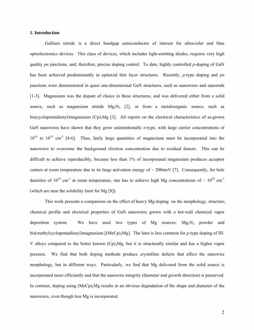
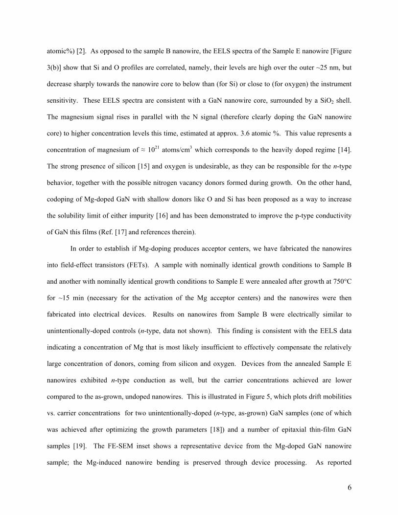
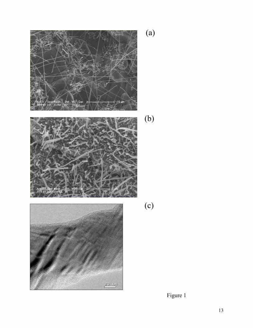
GaN nanowires. Figure 1 is a field emission scanning electron micrograph (FE-SEM) of representative
nanowires grown using (MeCp)2Mg at two very different increasing flow rates: 59 nmol/min [Figure 1(a);
Sample A] and 186 nmol/min [Figure 1(b); Sample C]. A clear degradation of the nanowire morphology
is observed at high dopant flow rate [see Figure 1(b)], namely, the nanowires acquire a “tape-like”
morphology, with multiple kinks and variable diameter along the length of the nanowire. This
degradation is better demonstrated in Figure 1(c), which is a high resolution TEM micrograph of a
5
nanowire from Sample B. The Mg-doped GaN nanowire exhibits variable diameter indicative of high
numbers of dopant-induced defects.
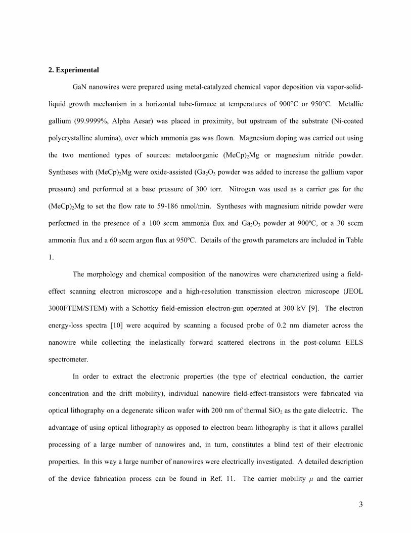
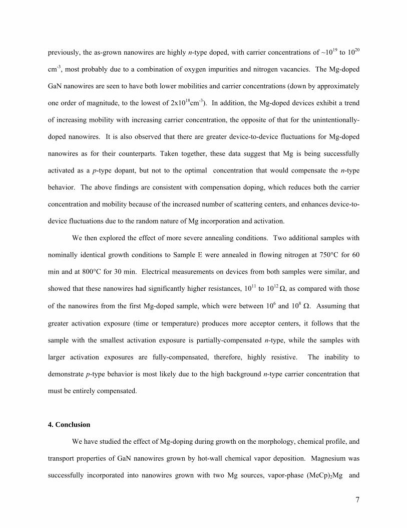
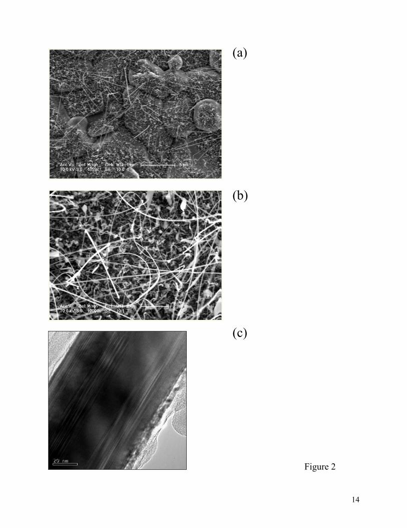
The effect of Mg incorporation into nanowires from the magnesium nitride powder source is
different. The nanowire morphology changes from straight in the undoped or lightly-doped case [Figure
2(a); Sample D] to highly bent at higher doping levels [Figure 2(b); Sample E]. Interestingly, though the
nanowires from Sample E are bent, their diameters are uniform and the growth direction is preserved.
This is better illustrated in the TEM of a representative nanowire in Figure 2(c). The streaks along the
axis of the nanowire are observed in the majority of the bent nanowires and have a similar appearance
with defects reported in bulk Mg-doped GaN [12] and MBE-grown Mg-doped GaN thin films [13],
indicating that they are most likely stalking faults along the c-axis direction of the wurtzite structure.
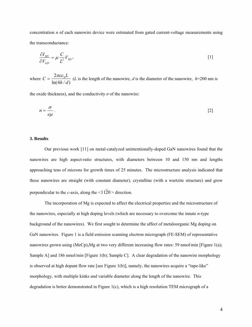
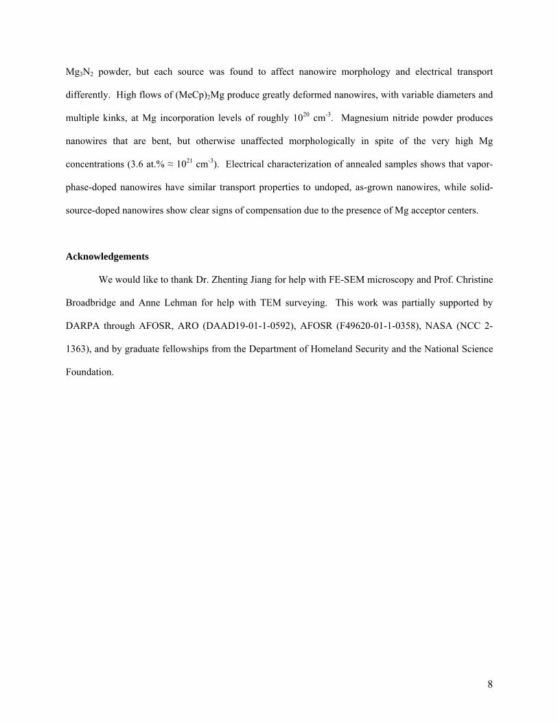
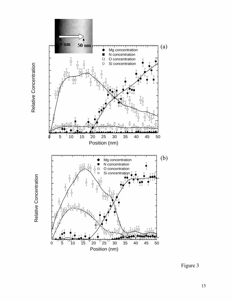
To study the incorporation of Mg into our nanostructures, we performed electron energy-loss
spectroscopy (EELS). The integrated spectrum intensities multiplied by the elemental cross-section
across two nanowires, one from Sample B [(MeCp)2Mg] and one from Sample E (Mg3N2), are shown in
Figures 3(a) and 3(b), respectively. The concentrations of four species—nitrogen, oxygen, silicon and
magnesium—are monitored in each plot. As illustrated in the FE-SEM inset in Figure 3(a), the profiles in
both panels begin (0 nm) at the nanowire edge and proceed towards the core. The onset of the nanowire
core corresponds to the onset of the nitrogen signal, which begins at ~20 nm. Silicon and oxygen are
present in both Sample B and Sample E nanowires, but with noticeable differences in their EELS profiles,
indicative of possible fundamental structural differences. Namely, the EELS spectra of Sample B [Figure
3(a)] show that the silicon level is constant throughout the wire, while the oxygen level is constant over
the outer 20 nm (position which corresponds to the onset of the nitride nanowire core), but afterwards
decreases gradually towards the core of the wire. This decrease appears to correlate with the increasing
nitrogen signal [see Figure 3(a)]. One possible interpretation of these EELS profiles would be a Si-doped
GaN core surrounded by an amorphous GaOx shell. Although Mg is present in the nanowire, it is barely
detectable, indicating a concentration of less than ca. 1 atomic %, which is the instrument sensitivity. This
is, however, consistent with expected Mg doping levels of approximately 1020 atoms/cm3 (≈ 0.23
6
atomic%) [2]. As opposed to the sample B nanowire, the EELS spectra of the Sample E nanowire [Figure
3(b)] show that Si and O profiles are correlated, namely, their levels are high over the outer ~25 nm, but
decrease sharply towards the nanowire core to below than (for Si) or close to (for oxygen) the instrument
sensitivity. These EELS spectra are consistent with a GaN nanowire core, surrounded by a SiO2 shell.
The magnesium signal rises in parallel with the N signal (therefore clearly doping the GaN nanowire
core) to higher concentration levels this time, estimated at approx. 3.6 atomic %. This value represents a
concentration of magnesium of ≈ 1021 atoms/cm3 which corresponds to the heavily doped regime [14].
The strong presence of silicon [15] and oxygen is undesirable, as they can be responsible for the n-type
behavior, together with the possible nitrogen vacancy donors formed during growth. On the other hand,
codoping of Mg-doped GaN with shallow donors like O and Si has been proposed as a way to increase
the solubility limit of either impurity [16] and has been demonstrated to improve the p-type conductivity
of GaN this films (Ref. [17] and references therein).
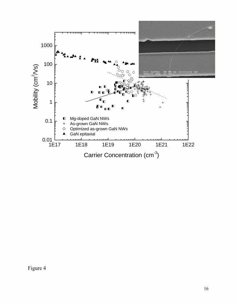
In order to establish if Mg-doping produces acceptor centers, we have fabricated the nanowires
into field-effect transistors (FETs). A sample with nominally identical growth conditions to Sample B
and another with nominally identical growth conditions to Sample E were annealed after growth at 750°C
for ~15 min (necessary for the activation of the Mg acceptor centers) and the nanowires were then
fabricated into electrical devices. Results on nanowires from Sample B were electrically similar to
unintentionally-doped controls (n-type, data not shown). This finding is consistent with the EELS data
indicating a concentration of Mg that is most likely insufficient to effectively compensate the relatively
large concentration of donors, coming from silicon and oxygen. Devices from the annealed Sample E
nanowires exhibited n-type conduction as well, but the carrier concentrations achieved are lower
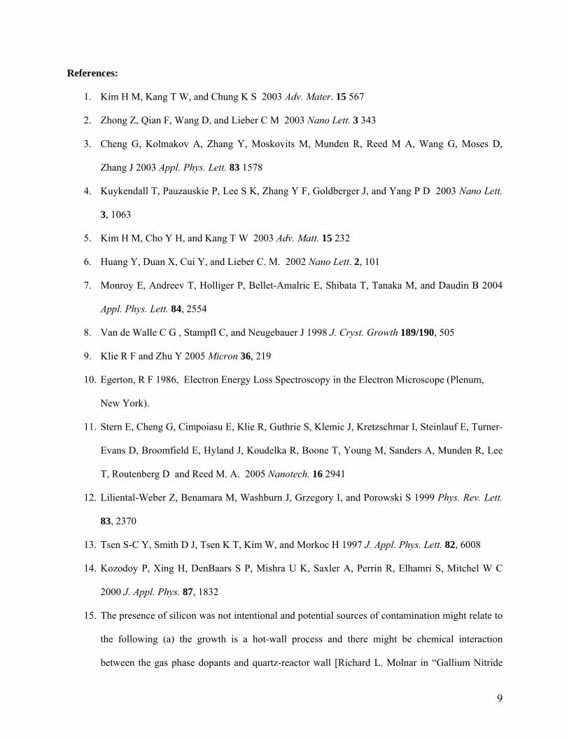
compared to the as-grown, undoped nanowires. This is illustrated in Figure 5, which plots drift mobilities
vs. carrier concentrations for two unintentionally-doped (n-type, as-grown) GaN samples (one of which
was achieved after optimizing the growth parameters [18]) and a number of epitaxial thin-film GaN
samples [19]. The FE-SEM inset shows a representative device from the Mg-doped GaN nanowire
sample; the Mg-induced nanowire bending is preserved through device processing. As reported
7
previously, the as-grown nanowires are highly n-type doped, with carrier concentrations of ~1019 to 1020
cm-3, most probably due to a combination of oxygen impurities and nitrogen vacancies. The Mg-doped
GaN nanowires are seen to have both lower mobilities and carrier concentrations (down by approximately
one order of magnitude, to the lowest of 2x1018cm-3). In addition, the Mg-doped devices exhibit a trend
of increasing mobility with increasing carrier concentration, the opposite of that for the unintentionally-
doped nanowires. It is also observed that there are greater device-to-device fluctuations for Mg-doped
nanowires as for their counterparts. Taken together, these data suggest that Mg is being successfully
activated as a p-type dopant, but not to the optimal concentration that would compensate the n-type
behavior. The above findings are consistent with compensation doping, which reduces both the carrier
concentration and mobility because of the increased number of scattering centers, and enhances device-to-
device fluctuations due to the random nature of Mg incorporation and activation.
We then explored the effect of more severe annealing conditions. Two additional samples with
nominally identical growth conditions to Sample E were annealed in flowing nitrogen at 750°C for 60
min and at 800°C for 30 min. Electrical measurements on devices from both samples were similar, and
showed that these nanowires had significantly higher resistances, 1011 to 1012 Ω, as compared with those
of the nanowires from the first Mg-doped sample, which were between 106 and 108 Ω. Assuming that
greater activation exposure (time or temperature) produces more acceptor centers, it follows that the
sample with the smallest activation exposure is partially-compensated n-type, while the samples with
larger activation exposures are fully-compensated, therefore, highly resistive. The inability to
demonstrate p-type behavior is most likely due to the high background n-type carrier concentration that
must be entirely compensated.
4. Conclusion
We have studied the effect of Mg-doping during growth on the morphology, chemical profile, and
transport properties of GaN nanowires grown by hot-wall chemical vapor deposition. Magnesium was
successfully incorporated into nanowires grown with two Mg sources, vapor-phase (MeCp)2Mg and
8
Mg3N2 powder, but each source was found to affect nanowire morphology and electrical transport
differently. High flows of (MeCp)2Mg produce greatly deformed nanowires, with variable diameters and
multiple kinks, at Mg incorporation levels of roughly 1020 cm-3. Magnesium nitride powder produces
nanowires that are bent, but otherwise unaffected morphologically in spite of the very high Mg
concentrations (3.6 at.% ≈ 1021 cm-3). Electrical characterization of annealed samples shows that vapor-
phase-doped nanowires have similar transport properties to undoped, as-grown nanowires, while solid-
source-doped nanowires show clear signs of compensation due to the presence of Mg acceptor centers.
Acknowledgements
We would like to thank Dr. Zhenting Jiang for help with FE-SEM microscopy and Prof. Christine
Broadbridge and Anne Lehman for help with TEM surveying. This work was partially supported by
DARPA through AFOSR, ARO (DAAD19-01-1-0592), AFOSR (F49620-01-1-0358), NASA (NCC 2-
1363), and by graduate fellowships from the Department of Homeland Security and the National Science
Foundation.
9
References:
1. Kim H M, Kang T W, and Chung K S 2003 Adv. Mater. 15 567
2. Zhong Z, Qian F, Wang D, and Lieber C M 2003 Nano Lett. 3 343
3. Cheng G, Kolmakov A, Zhang Y, Moskovits M, Munden R, Reed M A, Wang G, Moses D,
Zhang J 2003 Appl. Phys. Lett. 83 1578
4. Kuykendall T, Pauzauskie P, Lee S K, Zhang Y F, Goldberger J, and Yang P D 2003 Nano Lett.
3, 1063
5. Kim H M, Cho Y H, and Kang T W 2003 Adv. Matt. 15 232
6. Huang Y, Duan X, Cui Y, and Lieber C. M. 2002 Nano Lett. 2, 101
7. Monroy E, Andreev T, Holliger P, Bellet-Amalric E, Shibata T, Tanaka M, and Daudin B 2004
Appl. Phys. Lett. 84, 2554
8. Van de Walle C G , Stampfl C, and Neugebauer J 1998 J. Cryst. Growth 189/190, 505
9. Klie R F and Zhu Y 2005 Micron 36, 219
10. Egerton, R F 1986, Electron Energy Loss Spectroscopy in the Electron Microscope (Plenum,
New York).
11. Stern E, Cheng G, Cimpoiasu E, Klie R, Guthrie S, Klemic J, Kretzschmar I, Steinlauf E, Turner-
Evans D, Broomfield E, Hyland J, Koudelka R, Boone T, Young M, Sanders A, Munden R, Lee
T, Routenberg D and Reed M. A. 2005 Nanotech. 16 2941
12. Liliental-Weber Z, Benamara M, Washburn J, Grzegory I, and Porowski S 1999 Phys. Rev. Lett.
83, 2370
13. Tsen S-C Y, Smith D J, Tsen K T, Kim W, and Morkoc H 1997 J. Appl. Phys. Lett. 82, 6008
14. Kozodoy P, Xing H, DenBaars S P, Mishra U K, Saxler A, Perrin R, Elhamri S, Mitchel W C
2000 J. Appl. Phys. 87, 1832
15. The presence of silicon was not intentional and potential sources of contamination might relate to
the following (a) the growth is a hot-wall process and there might be chemical interaction
between the gas phase dopants and quartz-reactor wall [Richard L. Molnar in “Gallium Nitride
10
(GaN) II, Semiconductors and Semimetals”, vol. 57, ed. J.I. Pankove and T.D. Moustakas, 1999,
pg. 11] and (b) during few growth runs, oxide-covered silicon chips have been used as growth
substrates or support for the gallium species.
16. Reiss H, Fuller C S, and Morin F J, 1956 Bell Syst. Tech. J. 35, 535
17. Han B, Gregie J M, and Wessels B W, 2003 Phys. Rev. B 68 045205
18. Cimpoiasu E, Stern E, Cheng G, Munden R, Sanders A, and Reed M A Brazilian J. of Phys., in
press.
19. Rode D L and Gaskill D K 1995 Appl. Phys. Lett. 66 1972
11
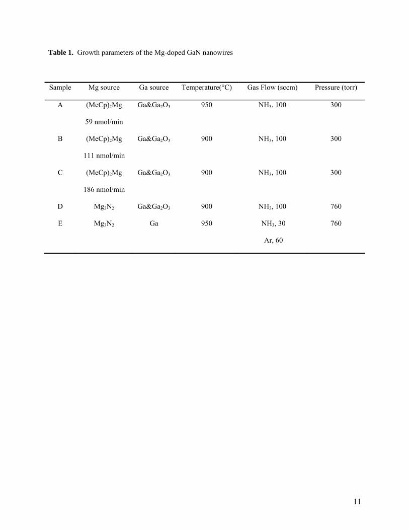
Table 1. Growth parameters of the Mg-doped GaN nanowires
Sample Mg source Ga source Temperature(°C) Gas Flow (sccm) Pressure (torr)
A (MeCp)2Mg
59 nmol/min
Ga&Ga2O3 950 NH3, 100 300
B (MeCp)2Mg
111 nmol/min
Ga&Ga2O3 900 NH3, 100 300
C (MeCp)2Mg
186 nmol/min
Ga&Ga2O3 900 NH3, 100 300
D Mg3N2 Ga&Ga2O3 900 NH3, 100 760
E Mg3N2 Ga 950 NH3, 30
Ar, 60
760
12
Figure captions:
Figure 1. FE-SEM micrographs of Mg-doped GaN nanowires grown using (MeCp)2Mg at (a) 59
nmol/min, Sample A and (b) 186 nmol/min, Sample C. (c) TEM micrograph of a (MeCp)2Mg-doped
GaN nanowire from Sample B.
Figure 2. FE-SEM micrographs of Mg-doped GaN nanowires grown using Mg3N2 powder at (a) 900°C,
Sample D and (b) 950°C, Sample E. (c) TEM micrograph of a Mg3N2-doped GaN nanowire from Sample
E.
Figure 3. Profiles of four species of interest, Si, O, N, and Mg for a representative nanowire from (a)
Sample B and (b) Sample E, as extracted using EELS. The solid lines represent the smoothed profiles.
The inset FE-SEM shows the direction and orientation of the scan, which begins at the nanowire edge (0
nm).
Figure 4. Plot of drift mobility vs. carrier concentration. Filled squares correspond to devices from
Sample E, while empty circles and crosses correspond to unintentionally-doped (as-grown) nanowires
[18]. Data from epitaxially-grown thin-film GaN [19] is plotted as filled triangles. The inset shows a
FE-SEM micrograph of a nanowire device.
13
Figure 1
(a)
(c)
(b)
14
Figure 2
(b)
(a)
(c)
15
Figure 3
(c)
0 5 10 15 20 25 30 35 40 45 50
Mg concentration N concentration O concentration Si concentration
Rel
ativ
e C
once
ntra
tion
Position (nm)
0 5 10 15 20 25 30 35 40 45 50
Mg concentration N concentration O concentration Si concentration
Rel
ativ
e C
once
ntra
tion
Position (nm)
(a)
(b)
16
1E17 1E18 1E19 1E20 1E21 1E220.01
0.1
1
10
100
1000
Mob
ility
(cm
2 /Vs)
Carrier Concentration (cm-3)
Mg-doped GaN NWs As-grown GaN NWs Optimized as-grown GaN NWs GaN epitaxial
Figure 4
![Metal-catalyzed semiconductor nanowires · Axial and radial impurity doping for both n-type ... 110 a comprehensive list 112 a GaAs 111 Ba/[0001] ... (a)(b) (c)(d) (e)(f)](https://img.pdfslide.net/doc/110x75/5acbc8bf7f8b9a93268babf1/metal-catalyzed-semiconductor-nanowires-and-radial-impurity-doping-for-both-n-type.jpg)

![Electrochemical water oxidation on WO3 surfaces A density ......reported experimentally that Mo doping leads to a favourable band gap for water oxidation [20]. Mo-doped WO 3 nanowires](https://img.pdfslide.net/doc/110x75/5e5d6bda668b5b5e614c3aa4/electrochemical-water-oxidation-on-wo3-surfaces-a-density-reported-experimentally.jpg)


![119 Nanowires 4. Nanowires - UFAMhome.ufam.edu.br/berti/nanomateriais/Nanowires.pdf · 119 Nanowires 4. Nanowires ... written about carbon nanotubes [4.57–59], which can be](https://img.pdfslide.net/doc/110x75/5abfd11e7f8b9a5d718eba2b/119-nanowires-4-nanowires-nanowires-4-nanowires-written-about-carbon-nanotubes.jpg)