Embed Size (px)
Citation preview

The Effects of Mechanical Stress on Semiconductor Devices
by
Safina Hussain
A dissertation submitted to the Graduate Faculty of
Auburn University
in partial fulfillment of the
requirements for the Degree of
Doctor of Philosophy
Auburn, Alabama
May 9, 2015
Approved by
Jeffrey C. Suhling, Chair, Quina Distinguished Professor of Mechanical Engineering
Richard C. Jaeger, Co-Chair, Distinguished University Professor Emeritus of Electrical
and Computer Engineering
Hareesh V. Tippur, McWane Professor of Mechanical Engineering
Michael C. Hamilton, Assistant Professor of Electrical and Computer Engineering
ii
Abstract
Mechanical strains and stresses are developed during the fabrication, assembly
and packaging of the integrated circuit (IC) chips. Sources include processes such as
shallow trench isolation, wafer backgrinding and dicing, TSV formation, die attachment,
and first level packaging (e.g. encapsulation). These stresses and strains cause parametric
shifts in the electronic components which change their electrical performance, and can
result in devices operating out of specification.
The influence of mechanical stress on devices that operate using conduction of
majority carriers is often modeled using piezoresistive theory. Extensive investigation has
been done on mechanical stress effects on resistors fabricated on integrated circuit chips.
In addition, test chips using resistor sensors have been successful in measuring die
stresses for various packaging architectures. Stress effects on diodes, field effect
transistors (FETs), van der Pauw structures, and CMOS sensor arrays have also been well
characterized. The influences of mechanical stress/strain on bipolar junction transistors
(BJT) are more complicated than those for other devices. This is because bipolar
transistors feature conduction in both n-type and p-type regions, as well as conduction of
minority carriers.
In prior studies, the influence of stress on BJT behavior has been described using
the so-called piezojunction effect, which includes variations in the minority carrier
mobility and the intrinsic carrier concentration. Whereas the piezoresistive effect

iii
describes the variation of the resistivity components of the majority carriers with applied
mechanical stress, the piezojunction effect governs the dependence of the minority carrier
conduction on stress.
In BJTs, both bandgap and the attendant mobility variations influence various
parameters including saturation current IS, collector current IC, base current IB, and DC
current gain β. Analog circuits containing bipolar transistors are also affected by stress,
including precision voltage references, op-amps, A/D and D/A converters, etc.
Experimental data for resistors and resistive channels of CMOS devices have
demonstrated that their changes in their electrical characteristics can be explained by
linear piezoresistive theory that includes only first order terms. However, most data for
bipolar transistors in the literature illustrate non-linear variations of saturation current,
collector current, and base current with applied uniaxial stress.
In this dissertation, mechanical stress related phenomena for several electronic
devices including resistors, field effect transistors, and bipolar transistors have been
explored. In the first portion of this work, measurement and other errors have been
investigated for multi-element resistor sensor rosettes on (111) silicon. Resistors are
widely used in the semiconductor industry as silicon stress sensors. They are fabricated
on the surface of test chips and then used to extract stresses over the die surface. To make
such measurements, the user must measure the changes in the resistances of the sensors,
the piezoresistance coefficient values, and the temperature. These experimental
measurements inherently contain certain uncertainties in their values. In this work, an
error analysis was performed, which included uncertainties in measurements and
calibration constants. This sensitivity analysis included direct calculations of the
iv
sensitivities of the extracted stresses to uncertainties in the calibrated piezoresistive
coefficients, measured sensor resistances, and the measured temperature.
In the second portion of this work, calibration of field effect transistor (FET)
stress sensors was investigated. Stress effects on FETs can be modeled using
piezorsistive theory similar to resistors. In this dissertation, the dependence of the
piezoresistive coefficients on the drain current operating point of the FET device has
been explored. Both the PMOS and NMOS devices demonstrated strong drain current
dependencies. The piezoresistance coefficients were also expressed as a function of
carrier mobility in the channel region.
In the third and final portion of this work, stress effects on bipolar junction
transistors have been investigated. The primary goal of this research topic was to
understand and model the impact of mechanical stress on bipolar transistors and precision
analog circuits. Although piezojunction coefficients have previously been proposed in the
literature to describe the variation of transistor saturation currents under stress, there has
not been a comprehensive modeling effort for use in circuit simulation. In this
dissertation, a basic charge-control model for the transistor has been proposed that
adequately captures the macroscopic impact of stresses on the BJT device characteristics.
In addition, the developed approach has been used to model the influence of stress on
analog circuits employing these devices. This work has provided an understanding of the
dominant effects of stress on the basic BJT model parameters.
To support the proposed models, the response of BJTs to the controlled
application of mechanical stress has been characterized experimentally. Test structures
have been utilized to characterize the stress sensitivity of vertical bipolar devices
v
fabricated on both (100) and (111) silicon wafers. Uniaxial normal stresses were applied
using a four-point-bending fixture, and changes in the electrical performance of the BJTs
were observed. The experimental data acted as a benchmark in the development of the
theoretical model, and the developed stress equations for the BJT have been shown to
have excellent correlations with the experimental results. Based upon the current gain and
saturation current data, a methodology has been developed for properly separating the
contributions of intrinsic carrier concentration and minority carrier mobility on the
overall stress induced variations of the collector current and current gain of the BJT. In
the future, the developed formulations can be applied to theoretically optimize transistor
design, placement, orientation, and processing to minimize the impact of fabrication and
packaging induced die stresses.

vi
Acknowledgments
I would like to first thank God for all the mercy and blessings in my life. I would
like to take this privilege to express my sincere gratitude to my major advisor Dr. Jeffrey
C. Suhling for his continuous support, supervision and guidance throughout my whole
Ph.D. work. I consider myself very lucky to have such a knowledgeable and extremely
talented mentor as my advisor. I am extremely thankful to my co-advisor Dr. Richard C.
Jaeger for his relentless help, direction, and insightful discussions without which it would
have been extremely difficult for me to work on my research topic. I would like to extend
my appreciation to my advisory committee members, Dr. Hareesh V. Tippur, Dr. Michael
C. Hamilton, and Dr. Bogdan M. Wilamowski for their time in serving on my committee
and their advices regarding my research work. My heartfelt appreciation goes to Mr.
Mike Palmer for his continuous assistance in helping with the wirebonding of the
samples for the experimental work of this dissertation. Special thanks goes to Mr. John
Marcell for the help he extended, for his suggestions and encouragement. I would also
like to take this opportunity to thank my all my lab mates and colleagues for their
friendship and support. Financial support from CAVE and SRC is greatly acknowledged.
This dissertation would not have been possible without the love, support,
encouragements and sacrifices of my parents A. K. Moazzem Hussain and Rasheda
Moazzem and my siblings Mahnur Fatima and Dr. A. H. M. Shahadat Hussain, and my
sister in law Dr. Sabrina Wahid. I am grateful to my friends at Auburn, Dr. Eliza Banu,
vii
Shaima Nahreen, Shakharupa Chowdhury, and especially to Dr. Shobnom Ferdous for
their friendship and support. Last but not the least, my husband Faisal Ahmed, who
himself is on the difficult journey to earn a Ph.D. at another university, I thank him for
his patience, support and for being there by my side, which was paramount to the
completion of my Ph.D.
viii
Table of Contents
Abstract .............................................................................................................................. ii
Acknowledgments ............................................................................................................ vi List of Tables .................................................................................................................... xi List of Figures ................................................................................................................. xiii
CHAPTER 1 ....................................................................................................................... 1 INTRODUCTION............................................................................................................. 1
1.1 Advancement of the Semiconductor Industry......................................................1 1.2 Mechanical Stress in Semiconductor ...................................................................2
1.2.1 Fabrication Induced Thermal Stress ............................................................... 3 1.2.2 Stress Due to Lattice Mismatch ...................................................................... 7 1.2.3 Intrinsic Stress ................................................................................................. 8
1.2.4 Electronic Packaging Induced Stress .............................................................. 9 1.3 Impact of Mechanical Stress in Electronics .......................................................13
1.4 Objectives of this Research ................................................................................17 1.5 Organization of the Dissertation ........................................................................18
CHAPTER 2 ..................................................................................................................... 20
LITERATURE REVIEW .............................................................................................. 20 2.1 Introduction ........................................................................................................20 2.2 Piezoresistive Effect...........................................................................................21
2.3 Sensors Based on Piezoresistive Effect .............................................................23 2.4 Piezojunction Effect ...........................................................................................30
2.5 Sensors Based on Piezojunction Effect..............................................................35 2.6 Effect of Stress on Semiconductor Band Structure ............................................36
2.7 Summary ............................................................................................................40
CHAPTER 3 ..................................................................................................................... 41
ERROR ANALYSIS FOR PIEZORESISTIVE STRESS SENSORS USED IN FLIP
CHIP PACKAGING ....................................................................................................... 41
3.1 Introduction ........................................................................................................41 3.2 Piezoresistive Theory for Silicon .......................................................................42
3.2.1 (100) Silicon.................................................................................................. 42 3.2.2 (111) Silicon.................................................................................................. 45
3.3 Rosette Designs ..................................................................................................46 3.3.1 Optimized 4-Element Rosette on (100) Silicon ............................................ 48 3.3.2 Optimized 8-Element Rosette on (111) Silicon ............................................ 50
3.4 StressExtraction using Piezoresistive Theory ....................................................53
ix
3.5 Sensitivity Analysis ...........................................................................................53
3.5.1 Resistance Measurement Errors .................................................................... 55 3.5.2 Temperature Measurement Errors ................................................................ 56 3.5.3 Piezoresistive Coefficient Uncertainty ......................................................... 57
3.6 Finite Element Modeling ...................................................................................58 3.7 Discussion of Results .........................................................................................60
3.7.1 Review of Piezoresistive Coefficient Sensitivities ....................................... 60 3.7.2 Sensitivities to Temperature Measurement Errors ........................................ 67 3.7.3 Sensitivities to Resistor Measurement Errors ............................................... 67
3.7.4 Monte Carlo Analysis ................................................................................... 70 3.8 Summary and Discussion ...................................................................................73
CHAPTER 4 ..................................................................................................................... 75
CURRENT DEPENDENCE OF THE PIEZORESISTIVE COEFFICIENTS OF
MOSFETS ON (100) SILICON ..................................................................................... 75
4.1 Introduction ........................................................................................................75 4.2 Metal Oxide Semiconductor Transistors ...........................................................76
4.3 Piezoresistive MOS Sensors ..............................................................................80 4.4 Experimental Method.........................................................................................82 4.5 Experimental Results .........................................................................................84
4.5.1 PMOS Calibration Results ............................................................................ 86 4.5.2 NMOS Calibration Results ........................................................................... 86
4.6 Correlation with Mobility ..................................................................................88 4.7 Summary and Discussion ...................................................................................90
CHAPTER 5 ..................................................................................................................... 92
CHARACTERIZATION OF THE IMPACTS OF MECHANICAL STRESS ON
THE PERFORMACE OF BIPOLAR JUNCTION TRANSISTORS ....................... 92 5.1 Introduction ........................................................................................................92
5.2 Bipolar Transistors .............................................................................................96 5.3 Experimental Procedure ...................................................................................101
5.3.1 Mechanical Stress Generation..................................................................... 101 5.3.2 Electrical Measurements ............................................................................. 108
5.4 Experimental Results .......................................................................................110 5.4.1 Base-Emitter Voltage VBE Sweep Method ................................................. 110 5.4.2 Fixed Base-Emitter Voltage VBE Method ................................................... 117 5.4.3 Emitter Current IE Sweep Method ............................................................... 127
5.5 Summary and Conclusions ..............................................................................132
CHAPTER 6 ................................................................................................................... 134
THEORETICAL MODELING OF MECHANICAL STRESS EFFECT ON THE
PERFORMACE OF PRECISION ANALOG DEVICES ......................................... 134 6.1 Introduction ......................................................................................................134 6.2 Bipolar Junction Transistor Modeling .............................................................137 6.3 Piezoresistive Theory .......................................................................................142
6.3.1 (100) Silicon................................................................................................ 142

x
6.3.2 (111) Silicon................................................................................................ 144
6.4 Transistor Theory .............................................................................................144 6.4.1 npn Transistors on (100) Silicon ................................................................. 146 6.4.2 pnp Transistors on (100) Silicon ................................................................. 147
6.4.3 Current Gain................................................................................................ 148 6.4.4 Overall npn and pnp Stress Dependencies .................................................. 151 6.4.5 Temperature Dependencies ......................................................................... 152 6.4.6 Simplifications and Numerical Estimates ................................................... 153
6.5 Intrinsic Carrier Concentration (ni) ..................................................................154
6.6 Minority Carrier Piezoresistive Coefficients ...................................................155 6.6.1 Piezoresistive Coefficient Simplifications .................................................. 157 6.6.2 Theoretical Model for Uniaxial Stress ........................................................ 160 6.6.3 (111) Silicon................................................................................................ 169
6.6.4 Systematic Approach to Parameter Extraction ........................................... 170 6.7 Conclusions ......................................................................................................170
CHAPTER 7 ................................................................................................................... 172
MECHANICAL STRESS EFFECTS ON BIPOLAR ANALOG CIRCUITS ........ 172 7.1 Introduction ......................................................................................................172 7.2 Stress Induced Changes in Circuit Output .......................................................172
7.2.1 Stress Response of the Offset Voltage of Differential Pairs ....................... 174 7.2.2 Stress Response of PTAT Circuit ................................................................ 177
7.2.3 Stress Response of Current Mirror ............................................................ 179 7.3 Conclusion .......................................................................................................182
CHAPTER 8 ................................................................................................................... 183
CONCLUSIONS ........................................................................................................... 183
REFERENCES .............................................................................................................. 188
APPENDIX A ................................................................................................................. 208
PIEZORESISTANCE IN RESISTORS AND FIELD EFFECT TRANSISTORS . 208 A.1 Introduction ......................................................................................................208
A.2 Piezoresistive Theory for Silicon .....................................................................208 A.3 Piezoresistive Theory for Resistors .................................................................210 A.4 Piezoresistance Equations for Silicon Wafer Planes .......................................212 A.5 Piezoresistive Theory for Field Effect Transistors (FETs) ..............................218 A.6 Reference .........................................................................................................223
APPENDIX B ................................................................................................................. 225
APPENDIX C ................................................................................................................. 227 SENSITIVITIES FOR (111) SILICON ...................................................................... 227

xi
List of Tables
Table 1.1 Thermal Expansion Coefficients of Some Materials Used ................................ 4
Table 1.2 Packaging Disciplines [13] .............................................................................. 10
Table 3.1 Piezoresistive Coefficients for Ligthly Doped Silicon [23] ............................. 44
Table 3.2 Typical Coefficient Data (oC, 1/TPa, ppm/oC) ................................................. 59
Table 3.3 Stress Sensitivities with respect to Errors in the “B” Coefficients and
Temperature .................................................................................................... 65
Table 3.4 Fractional Error - Worst Case Total ................................................................ 67
Table 3.5 Derivatives with Respect to Temperature ........................................................ 68
Table 3.6 Derivatives of Stress with Respect to Errors in Measured Resistor Values .... 68
Table 3.7 Monte Carlo Results 100 Cases (MPa) ........................................................... 73
Table 4.1 Classic Piezoresistive Coefficients for Lightly-Doped Silicon from C. S. Smith
[23] .................................................................................................................. 82
Table 5.1 Δβ/β vs σ Slope Values for Different npn Bipolar Transistor ....................... 114
Table 6.1 Vertical Transistor Stress Dependencies for (100) Silicon ............................ 151
Table 6.2 Vertical Transistor Stress Dependencies for (111) Silicon ............................ 152
Table 6.3 Vertical Transistor Theory Temperature Dependencies ................................ 153
Table 6.4 Quadratic Fits to Theoretical Plots of Creemer [171].................................... 156
Table 6.5 Piezoresistive Coefficients in Lightly-Doped Silicon [41] ............................ 158
Table 6.6 Piezoresistive Coefficient Estimates for Silicon Bipolar Transistors ............ 159
Table 6.7 Simplified Piezoresistive Coefficient Estimates for Silicon Bipolar Transistors
........................................................................................................................ 159

xii
Table 6.8 Simplified Stress Dependencies – (100) silicon ............................................ 160
Table 6.9 Simplified Stress Dependencies – (111) Silicon............................................ 161

xiii
List of Figures
Figure 1.1 Moore’s Law for Memory Chips and Microprocessors ................................... 2
Figure 1.2 Various Sources of Mechanical Stress Generation in an IC ............................. 4
Figure 1.3 Stress Distribution Near a Shallow Trench Isolation ....................................... 5
Figure 1.4 Finite Element Simulation of the Horizontal Normal Stress Distribution Near
TSVs (Top View) [8] ...................................................................................... 7
Figure 1.5 (a) Strain Induced due to the Lattice Mismatch Between Silicon and Silicon-
Germanium (b) Difference in Bandgap between Silicon and Silicon-
Germanium ...................................................................................................... 8
Figure 1.6 Stress Distribution due to Compressive CESL in a PMOS (left), .................... 9
Figure 1.7 TI Packaging Technology Trends .................................................................. 11
Figure 1.8 Packaging Hierarchy ...................................................................................... 12
Figure 1.9 Typical CBGA Packaging Architecture ........................................................ 13
Figure 1.10 Flip Chip Packages Potential Fail Locations ................................................ 15
Figure 3.1 (100) Silicon Wafer ........................................................................................ 43
Figure 3.2 (111) Silicon Wafer ........................................................................................ 45
Figure 3.3 A Four-Element Rosette for (100) Silicon ..................................................... 48
Figure 3.4 Top: A Sensor Rosette for (111) Silicon. Bottom: Microphotograph of the
Sensor Rosette. ................................................................................................ 51
Figure 3.5 Flip-Chip Package and the Finite-Element Model ......................................... 58
Figure 3.6 Simulation Results for '11. ............................................................................ 59
Figure 3.7 Simulated Normal Stress Fields on the Die Surface ...................................... 60

xiv
Figure 3.8 Shear Stress Fields Across the Die ................................................................. 61
Figure 3.9 Sample Sensitivities of the In-Plane Normal Stress ....................................... 62
Figure 3.10 Sample Sensitivities of the In-Plane Normal Stresses .................................. 62
Figure 3.11 Sensitivity of Shear Stresses (Temperature Compensated) .......................... 63
Figure 3.12 Sensitivity of Shear Stresses (Temperature Compensated) .......................... 63
Figure 3.13 Fractional Errors for InPlane Normal Stresses to a 5˚K ............................... 64
Figure 3.14 Sample Sensitivities of σ'11 with respect to Errors in (a) ΔR1/R1 (b) ΔR3/R3
(c) ΔR5/R5 (d) ΔR7/R7 .................................................................................. 69
Figure 3.15 Sample Sensitivities of σ'22 with respect to Errors in (a) ΔR1/R1 (b) ΔR3/R3 (c)
ΔR5/R5 (d) ΔR7/R7 ....................................................................................... 69
Figure 3.16 Monte Carlo Process Steps ........................................................................... 72
Figure 4.1 Schematic Diagram of an NMOS (left) and PMOS (right) Transistors ......... 77
Figure 4.2 Conceptual Layouts of 0/90o PMOS and ±45o NMOS .................................. 80
Figure 4.3 (001) Silicon Wafer Coordinates .................................................................... 81
Figure 4.4 PMOS (left) & NMOS (right) Sensor Circuits ............................................... 81
Figure 4.5 Flexible Circuit Used to Interface to Wafer Strip .......................................... 83
Figure 4.6 Four Point Bending Fixture ............................................................................ 83
Figure 4.7 Typical Responses of the PMOS and NMOS Transistors .............................. 84
Figure 4.8 Extracted Values of p p
44 S and vs. PMOS Drain Current............................ 85
Figure 4.9 Extracted n n
S D and vs. NMOS Drain Current ............................................. 87
Figure 4.10 Measured NMOS and PMOS TCs vs. Drain Current................................... 88
Figure 4.11 p p
44 S and vs. Hole Mobility in the PMOS Channel ................................ 89
Figure 4.12 nS vs. Electron Mobility in the NMOS Channel ........................................ 90

xv
Figure 5.1 Normalized Change in Current Gain vs. Uniaxial Stress for a Vertical Bipolar
Transistor ....................................................................................................... 95
Figure 5.2 Simplified Schematic a Vertical npn Bipolar Transistor ................................ 97
Figure 5.3 Vertical and Lateral Bipolar Transistors ........................................................ 98
Figure 5.4 Output Characteristic Plot for a Bipolar Transistor ........................................ 99
Figure 5.5 Gummel Plot for an npn Bipolar Transistor ................................................. 100
Figure 5.6 DC Current Gain vs. Base-Emitter Voltage for High Performance npn Bipolar
Transistor.......................................................................................................100
Figure 5.7 Bipolar Transistor Wafer Strip on (100) Silicon .......................................... 102
Figure 5.8 Bipolar Transistor Test Structures on (100) Silicon ..................................... 103
Figure 5.9 Bipolar Transistor Test Structures on (111) Silicon ..................................... 103
Figure 5.10 Four Point Bending Test Fixture ................................................................ 104
Figure 5.11 Four Point Bending of Wafer Strip ............................................................ 105
Figure 5.12 Noisy Data due to Probing Force Errors .................................................... 106
Figure 5.13 Flexible Circuit Used to Interface to Wafer Strip ...................................... 107
Figure 5.14 Flexible Circuit and Interface Box ............................................................. 107
Figure 5.15 Schematic Diagram of the Test Structure ................................................... 108
Figure 5.16 The Forward Biasing of the npn (Right) and pnp (Left) Transistor ........... 109
Figure 5.17 Changes in npn Bipolar Transistor Characteristics Due to Stress .............. 111
Figure 5.18 Change in Gummel Plots with Stress npn Bipolar Transistor .................... 111
Figure 5.19 Change in Current Gain vs. Base-Emitter Voltage .................................... 112
Figure 5.20 Normalized Change in Current Gain vs Stress npn Bipolar Transistor...... 112
Figure 5.21 Normalized Change in Current Gain with Stress for Several npn Bipolar
Transistor ................................................................................................... 113
Figure 5.22 Normalized Change in Current Gain vs. Stress .......................................... 114
xvi
Figure 5.23 Change in Gummel Plots with Stress pnp Bipolar Transistor .................... 115
Figure 5.24 Change in Current Gain vs. Base-Emitter Voltage Response with Stress for
pnp Bipolar Transistor ............................................................................... 116
Figure 5.25 Change in Current Gain vs. Base-Emitter Voltage Response with Stress for
pnp Bipolar Transistor ............................................................................... 116
Figure 5.26 Changes in the Current Gain with Applied Uniaxial Stress (Left) Changes in
the Currents with Applied Uniaxial Stress (Right) .................................... 117
Figure 5.27 Gummel Plot for an npn Transistor (Left) Changes in the Currents of the
Same Transistor with Stress (Right) ......................................................... 119
Figure 5.28 Attempts Made to Improve Change in the npn Currents on (100) Silicon . 120
Figure 5.29 Normalized Change in the npn and pnp Currents on (100) Silicon ........... 121
Figure 5.30 Van der Pauw Structure .............................................................................. 121
Figure 5.31 Change in Current Gain and Currents of an npn Transistor on (111) Silicon
..................................................................................................................... 121
Figure 5.32 Change in Current Gain of an npn Transistor on (100) Silicon ................. 123
Figure 5.33 Change in Currents of an npn Transistor on (100) Silicon ......................... 124
Figure 5.34 Change in Current Gain of an pnp Transistor on (100) Silicon ................. 125
Figure 5.35 Change in Currents of an pnp Transistor on (100) Silicon ......................... 126
Figure 5.36 Temperature Dependence of Voltage VBE .................................................. 128
Figure 5.37 The Emitter Current IE Biasing of the npn (Right) and pnp (Left) Transistor
.................................................................................................................... 129
Figure 5.38 Change in Current Gain of an npn Transistor on (100) Silicon using IE
Sweep Method .......................................................................................... 130
Figure 5.39 Change in Saturation Current IS of an npn Transistor on (100) Silicon using
IE Sweep Method ....................................................................................... 131
Figure 5.40 Comparison Between Fixed VBE and Emitter Current IE Biasing Method 131
Figure 5.41 Change in Saturation Current IS of an pnp Transistor on (100) Silicon using
IE Sweep Method ....................................................................................... 132

xvii
Figure 6.1 Simplified Cross-Section of a Vertical npn Bipolar Transistor ................... 137
Figure 6.2 Change in Current Gain vs. Stress for a Sub-Micron npn Bipolar Transistor
................................................................................................................... 138
Figure 6.3 Stress Response of Gummel Plot for a npn Transistor ................................. 138
Figure 6.4 Current Gain vs. Base-Emitter Voltage and Stress for a npn Transistor ...... 139
Figure 6.5 Measured Early Voltage for an npn Transistor ............................................ 140
Figure 6.6 Principal and Primed Coordinate System for (a) (100) silicon and (b) (111)
Silicon ......................................................................................................... 143
Figure 6.7 One Dimensional npn Transistor .................................................................. 145
Figure 6.8 (Left) Demonstration of Early Effect in an 1D npn Transistor. (Right), The
Biasing Used for Early Effect ..................................................................... 149
Figure 6.9 Measured npn IC and VBE versus VCE(Left) Measured pnp IC and IB versus
VCE (Right)................................................................................................. 150
Figure 6.10 Calculations done by Creemer, et al. using kp method Employing Bir and
Pikus Deformation Potential Theory ......................................................... 156
Figure 6.11 Comparison of Majority and Minority Carrier Mobilities versus Impurity
Concentration ........................................................................................... 157
Figure 6.12 Comparison of pnp Collector Current with Theory ................................... 163
Figure 6.13 Comparison of pnp Base Current with Theory........................................... 164
Figure 6.14 Comparison of pnp Current Gain with Theory........................................... 164
Figure 6.15 Comparison of npn Currents with Theory .................................................. 165
Figure 6.16 Comparison of npn Currents with Theory .................................................. 167
Figure 6.17 Comparison of npn Current Gain with Theory........................................... 168
Figure 6.18 (111) Transistors Under Uniaxial Stress: npn Normal-Mode Current Gain
.................................................................................................................. 169
Figure 7.1 Bipolar Transistor Wafer Strip on (100) Silicon .......................................... 173

xviii
Figure 7.2 Application of Uniaxial Stress to Bipolar Circuits ....................................... 174
Figure 7.3 npn Differential Pair ..................................................................................... 174
Figure 7.4 Offset Voltage vs. Stress Plot of an npn Differential Pair ............................ 176
Figure 7.5 PTAT Circuit ................................................................................................. 177
Figure 7.6 PTAT Output Voltage vs. Uniaxial Stress ..................................................... 178
Figure 7.7 Current Mirror Circuit .................................................................................. 179
Figure 7.8 Output Current Change vs. Stress of Current Mirror Circuit (Theory) ........ 181
Figure 7.9 Output Current Change vs. Stress of Current Mirror Circuit (Experiment) . 181

1
CHAPTER 1
INTRODUCTION
1.1 Advancement of the Semiconductor Industry
The semiconductor industry at present is utilizing ultra-large-scale integrated
circuit (IC) technology and system-in-package technology to achieve smaller feature
sizes, higher transistor performance, more speed, and reductions in cost. We are living in
the world of high performance computers, tablets, high speed communication through
cellular phones, wireless application modules, GPS, PDAs, hand-held devices, and image
capturing devices. These are all possible due to tremendous technological developments
in the semiconductor industry such as the invention of integrated circuits and scaling of
semiconductor devices. The scaling down of transistors follows the famous empirical
observation by Gordon Moore, co-founder of Intel Corporation, which states that number
of transistors on a chip doubles approximately every two years (Fig. 1.1) with improved
performance from the previous technology node and reduced cost per transistor [1]. This
observation known as “Moore’s Law”, acts as a guidance for the semiconductor industry
to set goals for the development and engineering of the next technology node. With each
improvement, silicon technology downscaling results in more transistors on a single chip
and an increase in computational capability.
For last 40 years, down scaling of the minimum feature size from 10 µm to 10
nm has been the predominant factor for increasing device density and lowering the cost

2
of the integrated circuit chips. However, below 90 nm technology, planer transistor
technology has reached its practical downsizing limits [2]. To maintain Moore’s law
trajectories of performance improvement and to meet International Technology Roadmap
for Semiconductors (ITRS) targets, the semiconductor industry has adopted several new
innovative technologies and new materials such as strained silicon, multigate devices,
strained SiGe technology, as well as introducing high-K dielectric materials, metal gates
and so on. These new technologies and materials pose new challenges and complexity for
critical dimensions, mobility, variability, leakage, and reliability, greatly increasing the
capital cost and risk.
Figure 1.1 Moore’s Law for Memory Chips and Microprocessors (http://www.cmg.org)
1.2 Mechanical Stress in Semiconductor
Silicon integrated circuits are complex structures that consist of complicated
assemblies of various materials that are deposited, implanted, and grown at different

3
temperatures upto 1200˚ C. IC fabrication involves various processes such as silicon
crystal growth, photolithography, etching, thermal oxidation, deposition, and
implantation, etc. After fabrication, packaging of the ICs is performed using a wide range
of materials that provide structural reliability, electrical connection of the die to the PCB,
paths for heat dissipation, physical protection of the circuit, and environmental isolation
from mechanical and chemical hazards.
Mechanical strains and stresses are developed during Ic fabrication and packaging
steps. These stresses are often due to thermal expansion coefficient mismatches between
the wide variety of materials used in packaging. Other sources of stress generation
include intrinsic stresses in the deposited films, thermal oxidation of silicon, and
implantation of materials that have different lattice constants from that of silicon. Large
localized stresses can also occur in the silicon active area near the edges of the deposited
thin films, near embedded structures such as trenches, and in regions of material growth
such as local oxidation. Mechanical stress generating sources include processes such as
shallow trench isolation, wafer back grinding, dicing, TSV formation, die attachment, and
first level packaging (e.g. encapsulation) (Fig. 1.2). The demand for smaller geometric
circuits and increased circuit density make the stress distributions in silicon die more
complicated due to the complexity of device patterns. Sources of mechanical stress in
integrated circuit chip are reviewed in the references [3-5].
1.2.1 Fabrication Induced Thermal Stress
Materials expand when heated and contract when cooled down. During
fabrication and also during packaging, interaction of the different materials that constitute
the assembly, cause thermal stress to develop due to high temperature processing steps

4
and also temperature cycling during operation. Such thermal stresses develop due to
thermal expansion coefficient mismatches of the various utilized materials. Table 1.1
shows a list of thermal expansion coefficients of the materials typically used in silicon
fabrication and packaging.
Figure 1.2 Various Sources of Mechanical Stress Generation in an IC
Table 1.1 Thermal Expansion Coefficients of Some Materials Used
in the Semiconductor Industry
Material Thermal Expansion Coefficient, (10 -6)1/ C
Silicon 2.6
Silicon Oxide, SiO2 1
Silicon Nitride, Si3N4 3
Polysilicon 3.05
Aluminum 24
Copper 17
Pb-Sn Solder 24
Polyamide 40-50
Silica filled Epoxy 14-24
Ag-filled Epoxy 32
Shallow Trench Isolation BEOL Processing TSV Formation
Wafer Bonding Wafer Thinning PackagingWafer Dicing
5
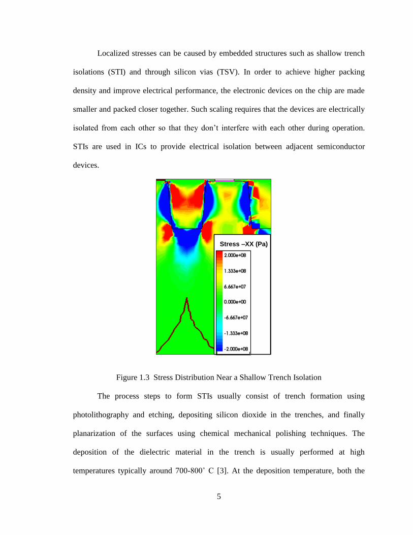
Localized stresses can be caused by embedded structures such as shallow trench
isolations (STI) and through silicon vias (TSV). In order to achieve higher packing
density and improve electrical performance, the electronic devices on the chip are made
smaller and packed closer together. Such scaling requires that the devices are electrically
isolated from each other so that they don’t interfere with each other during operation.
STIs are used in ICs to provide electrical isolation between adjacent semiconductor
devices.
Figure 1.3 Stress Distribution Near a Shallow Trench Isolation
The process steps to form STIs usually consist of trench formation using
photolithography and etching, depositing silicon dioxide in the trenches, and finally
planarization of the surfaces using chemical mechanical polishing techniques. The
deposition of the dielectric material in the trench is usually performed at high
temperatures typically around 700-800˚ C [3]. At the deposition temperature, both the
Stress –XX (Pa)
6
silicon and oxide are stress free. As the assembly is cooled down to room temperature,
the oxide contracts less than silicon due to the differences in the coefficients of thermal
expansion (CTE). This can result in high stresses on the order of several hundred of MPa
between the isolation edge of the silicon and oxide (Fig. 1.3) [6]. The stress magnitudes
drop as the distance from the isolation edge increases [6]. The mechanical stresses
generated from STIs have been observed to increase with downsizing of the devices.
Another such embedded feature that poses similar problem is the through silicon
via (TSV). The use of three-dimensional integrated circuit chips (stacking of chips) is the
recent trend in semiconductor industry to accommodate more functionally in smaller
space, improve power efficiency, and enhance performance [7]. TSVs have been
introduced in three-dimensional integration of chips to address the issue of increased
number of I/O from the chip. With the wirebonding or solder ball interconnects rapidly
reaching their practical density limits with the scaling of devices and increased device
density, TSV technology with interconnects embedded in the chip itself, have emerged as
a potential solution.
The fabrication steps for TSV usually are as follows: (i) etching silicon to form a
cylindrical through hole via, (ii) deposition of a seed layer on the side walls (iii) filling
the via with a conducting material such as copper. However, the differences in the
thermal expansion coefficients of the silicon and copper can cause significant stresses to
develop as shown in Fig. 1.4. These thermal stresses can cause the delaminations of the
copper, as well as degradations of the electrical performance of the transistors placed near
the TSV due to changes in mobility [8, 9].

7
Figure 1.4 Finite Element Simulation of the Horizontal Normal Stress Distribution Near
TSVs (Top View). [8]
1.2.2 Stress Due to Lattice Mismatch
With the scaling of silicon based devices approaching its downsizing limits,
researchers are actively looking for alternative methodologies to improve the
performance of the electronic devices. One such method widely used in recent times is
strain engineering or bandgap engineering, which mainly consists of adding other
materials to the silicon lattice to form silicon germanium (SiGe) or silicon carbide (SiC)
[10].
Adding germanium or carbon to the silicon substrate causes the band gap to
change. As shown in Fig. 1.5, there is a mismatch of the lattice constant of these
materials (silicon and germanium lattice constants are 1.17 and 1.22 Å, respectively). The
germanium lattice is 4.2% larger than that of silicon, and the diamond lattice is 45%
smaller than silicon. Therefore, a thin film of silicon epitaxially grown on top of SiGe or
SiC becomes strained due to the lattice mismatch [3]. This strain that is intentionally
induced in the silicon lattice enhances the performance of the transistors by improving
the mobility of the carriers. Such strain engineering is the latest trend that has been

8
adopted in state-of-the-art transistor technology to keep pace with Moore’s law, along
with other technological advancements.
(a)
(b)
Figure 1.5 (a) Strain Induced due to the Lattice Mismatch Between Silicon and Silicon-
Germanium
(b) Difference in Bandgap between Silicon and Silicon-Germanium [11].
1.2.3 Intrinsic Stress
Various semiconductor fabrication parameters such as thin film growth rate, thin
film thickness, temperature processing profiles, etc. can cause intrinsic stresses to
develop in silicon [5]. Deposition and growth of films cause unintentional stress to
develop. For example, localized large stress can be developed when a film is deposited on
a nonplaner surface [12]. Also, a substantial amount of stress can be developed during the
thermal oxidation of silicon, and this stress can cause discontinuities at the silicon-oxide
interface. One reason this stress develops is that the volume of the oxide that is grown is
2.2 times more than that of the silicon. As a result, compressive stress builds up in the

9
oxide [3]. During fabrication processes such as oxidation of trench sidewalls or the
selective oxidation of silicon nitride layers, stresses develop due to the volume expansion
associated with oxide formation. Stresses also develop when oxidation is done on a
nonplanar silicon surface. Convex or concave corners cause the oxidation layer to be
strained, resulting in a buildup of stress in the oxide. Oxidation induced stresses are a
common concern due to the pervasive use of thermal oxidations in silicon device
fabrication.
Intrinsic stress development in films during silicon fabrication is often
intentionally implemented in current technology nodes to improve the performance of the
devices. One such example is strained Contact-Etch-Stop-Layer (sCESL) technology as
shown in Fig. 1.6. Improvement of the performance of the transistors is accomplished by
utilizing the internal stresses developed in the silicon during silicon nitride passivation
processing.
Figure 1.6 Stress Distribution due to Compressive CESL in a PMOS (left),
Stress Distribution due to Compressive CESL in a NMOS (right) [3]
1.2.4 Electronic Packaging Induced Stress
After semiconductor fabrication, packaging of the chip is performed. Packaging
is a field which involves many disciplines, as shown in the Table 1.2 [13], and involves

10
complex engineering to establish links between the circuits on the chip and the system.
An electronic package is a composite assembly with different materials and geometrical
configurations, where one or more silicon chips are placed in an enclosure. The choice of
packaging for a particular product is driven by the demands for higher performance,
increased density of devices on the chip, increased reliability and cost reduction.
Table 1.2 Packaging Disciplines [13]
Discipline Problems addressed
Chemical Engineering Chemical Process Systems
Electrical Engineering Electronics and Electrical Design
Industrial Engineering Cost and Production Analysis
Mechanical Engineering Stress Analysis, Mechanical Design Tools
Materials Engineering Materials Selection, Metallization Process,
Wirebonding/ Solder Interconnects
Physics Electrical, Thermal and Mechanical Characteristics
Thermal Engineering Heat Transfer
Fig. 1.7 shows the evolution of packaging technologies over the last few decades,
which involves the use of various packaging architectures. This packaging road map for
Texas Instruments is typical of those used by other companies. Packaging can be
categorized in different ways; such as ceramic and plastic molded chip carriers. They can
also be classified in terms of their interconnection configuration, such as Quad Flat Pack
(QFP), Pin Grid Array (PGA), Ball Grid array (BGA) and Flip Chip (FC).

11
Figure 1.7 TI Packaging Technology Trends (http://www.monolithic3d.com/blog/archives/04-2012)
Fig. 1.8 illustrates a typical packaging hierarchy. One or more chips packaged in
protective chip carriers comprise the first level of packaging. The chip carriers usually
contain protective encapsulation materials such as ceramic or plastic as well as a
leadframe or substrate to provide a path for electrical connection to the outside system.
Wirebonding, solder interconnections, or tape automated bonding are technologies used
to electrically connect the chip to the leadframe or the substrate. The Printed Circuit
Board (PCB) containing the mounted chip carriers is referred to as the second level of
packaging. The chip carriers are connected to the PCB using either Plated Through Hole
(PTH) or the Surface Mount Technology (SMT). The third level packaging is the mother
board, where several printed circuit boards are connected together [14].

12
Figure 1.8 Packaging Hierarchy (http://www.ewh.ieee.org/soc/cpmt/press/pressimage.html)
Electronic packages consist of different materials having different geometries
with different mechanical properties. Elevated temperature processing of these materials
such as die attachment to the leadfame or substrate, plastic encapsulation, wirebonding,
and solder reflow causes thermal stresses to develop because of the mismatches in the
coefficients of thermal expansion of the different materials in the package. The heat
dissipated by high power devices can also cause thermal stresses to develop. For example,
Fig. 1.9 shows a typical CBGA packaging architecture for a high performance
microprocessor that consists of various materials in a complex geometrical configuration.
As indicated, the thermal expansion coefficients are widely different for the various
materials.
When systems are turned off, the packages cool down and the materials
comprising the package contract at different rates. Repetitive cooling and heating results

13
in thermal cycling, which causes fatigue loading of the package. Mechanical loadings can
also be caused by human interactions, such as shock/drop events and loads transferred to
the package from the contact with the printed circuit board. All the above mentioned
loadings cause complex biaxial (two-dimensional) or triaxial (three-dimensional) stresses
to develop in the package. Excessive stresses can affect the reliability of electronic
modules.
Figure 1.9 Typical CBGA Packaging Architecture
1.3 Impact of Mechanical Stress in Electronics
The possible stress generating processes in the fabrication and packaging of a
silicon chip have been discussed above. The impact of these stresses on the performance
of electronic devices will now be discussed. Mechanical stress is considered both
desirable and undesirable in semiconductor industry. Before the year 2000, stress was
Lid
Ceramic BGA Substrate
TIM1
TIM2
Heat Sink
Die
Lid
Adhesive
PCB Laminate

14
always considered to be undesirable in the processing and fabrication of the die, because
it was one of the reasons for defects, delamination, and performance degradation. As a
consequence, stresses were avoided at any cost [6, 15-17]. However, during the last
decade, stress has been intentionally introduced in selective regions of the devices to
enhance the circuit performance [18-21], although stress induced failures are still
considered unwanted.
Undesirable stresses are an unavoidable product of the fabrication or packaging of
semiconductor integrated circuits. When the stress in the silicon exceeds the material
strength, defects such as dislocations or slip patterns can occur in the silicon crystal [3].
During oxidation and ion implantation steps, nucleation of dislocations occur [12].
Dislocations can grow and move to other parts of a device boundary with further
accumulation of stress at later stages of fabrication and packaging that adversely affects
the circuit performance of the chip.
For area array packaging architectures, thermal cycling imposes the greatest
reliability challenge. As shown in Fig. 1.9, different components in packaging often have
different thermal expansion coefficients, different elastic moduli, and the components are
of different geometrical shapes. Thermal stresses that are developed due to these
differences in material properties can cause delaminations to occur at the component
interfaces due to repeated thermal cycling loadings. In addition, fatigue and creep under
stress can occur over a period of time, which can cause performance of the electronic
system to degrade. Fig. 1.10 shows typical failure sites and failure modes for a typical
flip chip package that occur as a consequence of mechanical stresses during thermal
cycling.

15
Figure 1.10 Flip Chip Packages Potential Fail Locations
Other than structural failure of the packages, thermal stress can also adversely
affect the performance of the devices on the chip. When stress is applied to a
semiconductor material, the electrical resistivity of the material changes, and such an
effect is called piezoresistance. In semiconductor materials such as silicon, stress alters
the positions of the conduction and valence bands, changing the band structure and band
gap. These effects change the carrier mobility of the device that results in change in
electrical resistivity of the material. Such changes in bandgap and carrier mobility cause
parametric shifts in the electronic devices and can cause device performance to degrade.
Although the semiconductor industry has considered stress as unwanted for 40+
years, the industry has now used stress effects to improve device performance by
changing carrier mobility and to boost the performance of the transistors on a silicon chip.
With the scaling of transistors reaching their practical minimum size limit due to the

16
leakage current at small gate lengths, the industry has been exploiting new technological
solutions to keep pace with Moore’s law beginning at the 90 nm technology node. To
continue with projected improvements in performance without changing the transistor
size, the semiconductor industry has opted to apply stress/strain into selected regions of
the device. Examples include the channel and source/drain in Metal-Oxide-
Semiconductor (MOS) transistors and in the base region of bipolar transistors. This
intentional inclusion of stress into silicon lattice, known as strain engineering or bandgap
engineering, is being widely implemented in nearly all submicron technology nodes.
Strained silicon technology is based on changing of the band structure of silicon due to
the presence of stress along appropriate crystallographic directions, and has been shown
to result in remarkable performance gain [22].
The beneficial effect of stress on the electron and hole mobilites has been known
since the 1950’s [23]. However, the industry did not start researching implementations of
this phenomena until the 1980’s [24, 25]. As mentioned above, improvements are often
obtained through straining the lattice of silicon by overgrowing silicon epitaxially above
a relaxed silicon-germanium (Si1-xGex) structure to significantly increase electron
mobility [11, 26]. Epitaxial growth of silicon on SiGe substrate causes the silicon to
assume the larger lattice constant of SiGe, and thus causes the silicon to be stressed
biaxially over the whole wafer. This technique of biaxially stressed silicon cannot be used
for both n-type (NMOS) and p-type (PMOS) transistors, since NMOS needs to be
stretched while PMOS should be compressed for performance enhancement. Thus, the
biaxial stress/strain technique is only beneficial for n-type transistors. Several alternative
uniaxial stress techniques have been developed for local stress generation. These

17
techniques include nitride contact etch stop liner [19], embedded SiGe growth in the
source and drain contacts [27], and even from shallow trench isolation [28] for high
volume manufacturing. Another method of stress generation to enhance performance is to
use tensile or compressive layers grown on top of a transistor depending upon whether
the transistor is of n-type or p-type. This method is called Dual Stress Liner (DSL), and
involves tensile layers of silicon-nitride grown on n-type transistors, and compressive
layers placed on top of p-type transistors. Using this method, the drain current can be
increased by up to 20% in p-type and 11% in n-type transistors [29, 30]. Some of these
local stress generating techniques are used simultaneously. For example, a stressed
nitride cap can be used along with embedded SiGe in the source and drain regions to
achieve even greater performance improvement [30, 31].
1.4 Objectives of this Research
The motivation of this work is to investigate issues related to mechanical stress in
semiconductor devices. The semiconductor devices investigated in this research are
resistors, field-effect transistors (FETs), and bipolar junction transistors (BJTs). This
dissertation also addresses the impact of mechanical stress on precision analog devices
and circuits. Three topics will be covered in this dissertation as outlined below:
1. Perform an error analysis for piezoresistive stress sensors used in flip chip
packaging.
- The objective of this work was to understand how errors made in the
measurements influence the stress extractions made subsequently with
multi element sensor rosettes on (111) silicon.

18
- A sensitivity analysis has been performed where direct calculations of the
sensitivities of the extracted stresses to uncertainties in the piezoresistive
coefficients and the measured temperature have been made.
2. Determination of the operating point dependence of the piezoresisitve coefficients
of CMOS Stress sensors on (100) silicon.
- The drain current dependence of the piezoresistive coefficients of NMOS
and PMOS field-effect transistors has been charaterized.
3. Develop a fundamental understanding required for characterization, modeling,
and mitigation of the impacts of mechanical stress on the performance of
precision analog devices (bipolar transistors).
- Measure and quantify the effects of stress on precision analog devices and
circuits.
- Develop a theoretical model based on the experimentally obtained to
predict the stress induced changes in the electrical characteristics of
bipolar transistors.
1.5 Organization of the Dissertation
This dissertation focuses on issues related to changes in electrical characteristics
of resistors, field effect transistors (FETs), and bipolar junction transistors (BJTs) caused
by presence of mechanical stress. The presentaton is organized into the following
chapters:
Chapter 1: The introduction chapter discusses the sources of mechanical stress in
integrated circuits (ICs). The sources include various processes during

19
fabrication and packaging of the IC. The impact of mechanical stress
on ICs is also discussed.
Chapter 2: A literature review on piezoresistivity, the piezojunction effect, and
the application of piezoresistive effect to sensors are presented
Chapter 3: Multi-element resistor stress sensor rosettes on (111) silicon are
discussed and the effects of uncertainties in the measured values of the
piezoresistive coefficients, sensor resistances, and the temperature on
the measurement results have been explored. Direct calculations of the
sensitivities of the extracted stresses to uncertainties in these
parameters are presented.
Chapter 4: The capability of metal oxide semiconductor field-effect transistors
(MOSFET) to be used as stress sensors is discussed, and the
dependence of the piezoresistance coefficients on the drain current of
the FET device is investigated.
Chapter 5: Experimental methods for characterizing the effects of mechanical
stress on bipolar transistor device characteristics are discussed and
experimental results are presented.
Chapter 6: A theoretical model to predict the stress induced changes in bipolar
junction transistor characteristics is developed, and then correlated
with the experimental results discussed on the Chapter 5.
Chapter 7: The effects of stress on selected integrated analog bipolar circuits are
explored and discussed.
Chapter 8: Summary and conclusions of the dissertation are presented

20
CHAPTER 2
LITERATURE REVIEW
2.1 Introduction
To achieve lower chip production cost, the semiconductor industry is working
towards incorporating more transistors per chip by downsizing the transistors and
improving performance of the transistors hence enhancing computational capability. As
the scaling down of the dimensions of the devices on chip continue, the stress patterns in
the chip are becoming more complex. Moreover packaging of the chip further
exacerbates the stress condition in the chip which may cause parametric shifts in device
performance, interconnect failure and damage yo the die and package. Therefore, stress
evolution during fabrication and packaging is a major reliability issue and great emphasis
is given in semiconductor industry on the studies of the effect of stress on the electronic
devices.
The stress effect on electronic devices such as resistors, field-effect transistors
(FETs) and bipolar junction transistors (BJTs) are referred to as piezoresistive or
piezojunction effects. Piezoresistance is a material property which causes electrical
resistance of the material to change due to the application of mechanical stress.
Stress/strain alters the symmetry of the semiconductor crystal and modulates the
conduction mechanism in semiconductors which results in variation in resistivity of the
material. The mechanical stress can be uniaxial tensile or compressive stress, hydrostatic

21
pressure, shear stress or a combination of these stresses. Depending on the semiconductor
material and crystallographic axis along which the stress is applied, there can be an
increase or decrease of the resistivity of the material. The piezoresistive effect is very
well understood since extensive research has been conducted in this area. The change in
the current of the p-n junction or the bipolar transistor due to the mechanical stress is
referred to as the piezojunction effect. Based on piezoresistive and piezojunction property
of silicon, micro-electro-mechanical-system (MEMS) sensors are designed and widely
used as strain gauges, accelerometers, cantilever force sensors, pressure sensors etc. [32-
36]. These sensors have the properties of high sensitivity, good linearity, small size,
mechanical sturdiness, the benefits of mass production due to microelectronic fabrication
techniques, and the ease of incorporation in standard IC technology [37].
2.2 Piezoresistive Effect
Widely used semiconductor materials silicon and germanium have a single cubic
crystal structure and these materials are extensively used as piezoresistors. Smith in 1954
first studied the piezoresistive behavior of germanium and silicon material [23]. He
conducted his measurements on lightly doped silicon and germanium samples and
measured large piezoresistive coefficients for these semiconductor materials compared to
metallic conductors. Smith’s coefficient values still serve as a reference to the upper
bound of these coefficients since as doping increases the value of piezoresistive
coefficients decreases. Smith measured first order piezoresistive coefficients for cubic
materials, which are reduced to three nonzero coefficients (π11: longitudinal, π12:
transverse and π44: shear) for silicon because of silicon’s diamond crystal structure. The
first utilization of the piezoresistive properties of germanium and silicon materials as

22
sensors to measure force, displacement and torque was done by Mason and Thurston in
1957 [38]. In their work they used bonded semiconductors as strain gauges to a test
sample, cut along different crystallographic directions to maximize the longitudinal
piezoresistive effect. In 1961, Pfann and Thurston talked about advantages of utilization
of transverse and shear piezoresistive effects along with the longitudinal effect [39]. In
their paper they discussed utilization of semiconductor strain gauges along different
crystallographic directions on either (100) or (111) surface to measure resistance change
of the gauges in terms of principal stresses, independent of the orientation of the gauge.
They also proposed incorporating diffused piezoresistive materials instead of bonded
strain gauges with a semiconductor force, torque or displacement sensing element. Kerr
and Milnes further investigated piezoresistive characteristics of the semiconductor
materials of a diffused layer on the semiconductor materials surface [40]. Tufte et al., in
1962 at Honeywell Research, were first to develop an integrated device using a
piezoresistive pressure sensing diaphragm formed by impurity diffusion which had
advantages over the bonded strain gauge diaphragm since the latter suffers from
hysteresis and creep problems [41]. In a paper published in 1964, Tufte and Stelzer
discussed experimental investigation of the effect of heavy doping and temperature on n-
type silicon [42]. The change in hole mobility due to piezoresistive effects on a silicon p-
type inversion layer was first studied by Colman et al [43].
The piezoresistive property of semiconductor has the disadvantages of
nonlinearity and temperature sensitivity. Investigation of nonlinearity is important for the
design of high precision sensors, since this nonlinearity must be avoided by selecting a
particular crystallographic direction or using some compensating circuits. The

23
nonlinearity exhibits a temperature dependence. Several researchers addressed the
nonlinearity of the semiconductor piezoresistance effect [33, 40, 44, 45], but they did not
address the issue quantitatively. Yamada et al. discussed the detailed measurement of
nonlinearity of p-type silicon diffused layers [46]. They proved that the third-order stress
terms gives good estimation for the piezoresistance effect and also showed that the
nonlinearity in the transverse mode is greater than the longitudinal nonlinearity. The
nonlinear piezoresistance of both n-type and p-type diffused layer were studied for
different stress and current directions by Matsuda and his coworkers [47, 48]. To
incorporate nonlinearity in the piezoresistance effect, Lenkkeri included nine nonzero
second-order piezoresistance coefficients for silicon along with the three first-order
coefficients determined by Smith [49].
A graphical representation of anisotropy of the piezoresistance effect of silicon is
represented by Kanda [50]. In his paper he plotted the longitudinal and transverse
piezoresistance coefficients at room temperature as a function of the crystal direction for
the (100), (110) and (211) surfaces. In another paper, Kanda showed graphical
representations of the shear piezoresistance coefficients as a function of the crystal
direction for the (100) plane [51].
2.3 Sensors Based on Piezoresistive Effect
Piezoresistive sensors are widely used for the characterization of complex stresses
developed in electronic package during operation of the electronic module. These sensors
are mainly resistor sensors which are implanted or diffused in the surface of the die in
suitable locations on the surface. These sensors are not mounted like traditional strain
gauges, rather they are fabricated in the surface of the die, hence an integral part of the

24
die. They can measure stresses nonintrusively even when the die is encapsulated. By
placing these sensors strategically over the surface of a test chip, full area array mapping
of the stresses over the die surface is possible. Piezoresistive sensors act as a guide
towards selection of manufacturing processes and materials, new package design,
prevention of package failures and improving reliability of electronic packages. The
capability of sensing stress in plastic encapsulated packages was first exploited by Texas
instruments in early 1980s [52-54]. Two-element sensor rosettes with 0-90 orientations,
capable of measuring in-plane normal stress at a particular point on the die surface on
(100) silicon were used by few early researchers such as Spencer et al. [54], Edwards et
al. [52, 53] and Beaty et al. [55]. Four-element sensor rosettes with 0-±45˚-90˚
configuration of either n- or p-type, that can measure all three in-plane stress components
were studied by Natarajan et al. [56] on (100) silicon and Gee et al. [57, 58] on (111)
silicon. Miura et al. introduced a sensor rosette capable of measuring three in-plane
stresses and one out-of-plane normal stress utilizing a four-element dual polarity rosette
with 0-90˚ n-type and ±45˚ p-type resistors [59-61, 67]. These sensors were used to
characterize thermally induced and packaging induced die stresses in DIPs.
Numerous papers on the application of the piezoresistive sensors to characterize
die stress was published by various researchers. Usell and Smiley in 1981 talked about
using test chips containing resistors sensors to quantify the strain induced due to the
molding process and change in temperature of plastic encapsulated Dual-Inline-Packages
(DIPs) [62]. Edwards et al. [52, 53], Spencer et al. [54] and Schroen et al. [63] performed
studies on plastic encapsulated packages to investigate the effect of fabrication process
variation, material variables and thermal cycling on the reliability of these packages. Test

25
chips on (111) silicon containing four-element sensor rosettes with 0-±45˚-90˚
orientations capable of measuring in plane stresses were used by Gee at el. [57, 58],
Nguyen et al. [64] and van Gestel [65] to map the distribution of stress across the surface
of die that were encapsulated in DIP packages. In these studies the researchers
investigated the location of the maximum normal stress and shear stress on the die
surface due to over molding of the DIP packages and thermal cycling. The effect of
package materials, assembly techniques and geometrical parameters on the stress
evolution were also explored. Lundström et al. explored the stress evolution of plastic
leaded chip carrier (PLCC) packages using stress sensors on (111) silicon [66].
Sweet et al. from Sandia national laboratories worked on several series of ATC
(ATC04, ATC06) test chips consisting of four n-type and four p-type resistors in each
cell at an orientations of 0-±45˚-90˚ with respect to a die edge [68-76]. Using these test
chips the researchers were able to extract three linear combination of the six unique stress
components. They measured the stresses in plastic encapsulated DIPs, QFNs and flip
chips [68, 70, 73, 74] and investigated the correlation of the stress evolution with the
stress induced damage in packaged integrated circuits [72].
The Suhling and Jaeger group from Auburn University have extensively
investigated the stress effects on resistors embedded on integrated chips and were
successful in characterizing die stresses for various packaging architectures [77-89]. This
group discovered the optimized sensor rosette on the (111) silicon which is capable of
measuring complete three-dimensional state of stress at any point on the surface of the
die as discussed by Bittle et al., Suhling et al. and Cordes et al [77, 78, 85]. To
characterize six stress components, both n-type and p-type eight element dual polarity

26
sensing elements in 0-±45˚-90˚ configuration are used since the piezoresistive
coefficients of n-type and p-type sensors are different [77, 78, 82]. They also presented
the general resistance change expression for resistors embedded in (111) silicon and
showed that four stress components can be measured in a temperature compensated
manner using this sensor rosette. Temperature compensated measurements should be
made whenever possible since there are large errors associated with the nontemperature
compensated stress terms if the exact temperature change is not known [79, 81]. Kang
worked out the piezoresistivity theory on various silicon wafer planes and also on silicon
carbide [89]. Thermally induced stress was measured by Suhling et al. by calibrating the
sensors over a wide temperature range [83]. A paper published by Jaeger et al. in 1993,
demonstrated the first use of off-axis rosette capable of measuring temperature
compensated results for both π44 and (π11–π12) [80]. Jaeger at al. discussed about the
sources of errors associated with the measurement of stresses using piezoresistive sensors
and discussed the methods to minimize the errors [79, 81]. Suhling et al. were first to use
a test chip to characterize the complete state of stress in plastic encapsulated die attached
to an FR-4 substrate [84]. To accurately measure the stresses developed in electronic
packages using test chips containing piezoresistive sensors, accurate determination of the
piezoresistive coefficients is necessary. Calibration of these coefficients is done using
four point bending, wafer level and hydrostatic methods [86, 90, 91]. Zou et al.
published papers on the stress characterization of PLCC, Chip on Board (COB), Quad
Flat Pack (QFP) and Pin Grid Array (PGA) packages using (100) and (111) silicon test
chips containing arrays of optimized piezoresistive stress sensor rosettes developed by
this group [92-96]. Finite element analysis was also performed to correlate the simulation

27
results with the experimental stress observations showing reasonable agreement. A
comprehensive review on piezoresistive theory and its application was published by
Suhling and Jaeger in 2001 [88]. Mian et al. from the same group investigated
analytically and experimentally a new piezoresistive stress sensor utilizing the van der
Pauw structure (VDP), and showed that this sensor has three times more stress sensitivity
than conventional resistor sensors [97, 98]. Rahim et al. used (111) test chips containing
the eight-element sensor rosettes to measure the die stresses on backside and device side
of the flip chip on laminate assemblies during various steps of assembly process and also
during thermal cycling [87, 99-103]. In these studies, the die stress evolution due to the
curing of the underfill was investigated for different underfill materials, and the residual
stresses present in the final cured assemblies were compared which aided the material
selection. These studies showed that in-plane shear stress provides an excellent indicator
of the initiation and growth of delamination between the underfill and die surface during
thermal cycling. The authors have also performed measurements of die stresses at
extremely low temperatures down to -180˚ C [99, 100]. Finite element analysis of flip
chip on laminate assemblies were presented in these papers and good agreement was
found with the obtained stress measurement data with the predictions of nonlinear finite
element models. Cho, Jaeger and Suhling [104] reported characterization of temperature
dependence of the piezoresistance coefficient for n-type and p-type silicon from -150˚C
to +125˚C using stress sensing chips. Roberts et al. utilized test chips to characterize die
surface stresses in flip-chip and Plastic Ball Grid Array (PBGA) packaging during
thermal cycling [105]. In more recent studies, Roberts et al. performed an extensive study
of die stresses in large flip-chip microprocessor die attached to a high CTE ceramic

28
substrate through lead free solder bumps [105-115]. In research performed on CBGA
packages, die stresses were measured after every packaging step (solder reflow, underfill
dispense and cure, and lid attachment), and the stresses were found to be increasing
monotonically. Die stresses were also measured during in-situ thermal cycling and power
cycling tests. A detailed sequential finite element analysis was performed to obtain stress
generation after each packaging stage and also during thermal cycling and power cycling
that incorporated thermal histories of the package, nonlinear temperature and time
dependent material properties and creation of elements. The simulation model showed
excellent correlation with the experimental data. In another study, Jaeger et al. and
Hussain et al. discussed the errors that arise in the stress extraction for a die on a flip chip
assembly due to the inherent uncertainty in the values of the piezoresistive coefficients as
well as measurement errors associated with measurement of rosette resistor values and
temperature [116-118]. A finite element simulation was performed to have an estimate of
the stresses that may occur on the die of a flip chip package and using the sensitivity
expressions derived by the authors, the sensitivities of extracted stress to resistor
measurement error, temperature measurement error and uncertainty in piezoresistive
coefficients values have been presented and discussed in these papers. Monte Carlo
simulations were utilized to estimate the expected errors in stress measurements of a
silicon die mounted in a typical flip chip package. The results indicated that the
sensitivities are stress dependent and vary widely over the die surface and it was shown
that the temperature compensated stress terms generally tend to have low sensitivity to
measurement uncertainty.

29
The device characteristics of both analog and digital circuits consisting of MOS
transistors change due to the fabrication and process induced stress [119-124]. So
extensive studies have been performed by various researchers to understand stress effect
son FETs [43, 123-128]. In an FET, the channel consist of a resistive region when the
transistor is biased in either linear or saturation region in strong inversion. With proper
biasing, mechanically applied stress changes the mobility of the carriers in the inversion
layer and makes FETs potential stress sensors. The advantage of the FET stress sensors
over the conventional resistor sensors is that these sensors occupy very small chip area
and as a result can be used to measure localized stress. Due to the light doping of the
channel region, the sensitivity of the FET sensors is much higher than the traditional
resistor sensors and also they can be operated in wide temperature range. In their paper,
Jaeger at el. characterized the stress induced changes in device parameters of the FETs
due to the piezoresistive channel region and commented on layout techniques to
minimize piezoresistive response of resistors and FETs in CMOS circuits [123]. In
another work, Jaeger at el. discussed relationships between CMOS circuit output and
temperature compensated stress components on the (100) silicon and suggested layout
techniques for optimized FET based piezoresistive sensor [129, 130]. A paper published
by in 1999 Bradley at el. talked about measuring package induced die stress for using test
chips containing 49 orthogonal CMOS FET sensor rosettes as stress sensors [131].
Bradley et al. showed in a later paper that the stress sensitivity of the FET channel does
not depend on the channel length and showed that parasitic resistance is the reason for the
observed reduction in piezoresistive coefficients of short-channel devices [132]. Chen et
al., reported implementation of 512 CMOS current mirror type stress sensors in a test

30
chip to map stress distribution over the chip surface with high resolutions and compared
the experimentally obtained data with that of finite element simulations for several
packaging test cases, yielding good correlation [133, 134]. In a recent work performed by
Hussain et al., it has been demonstrated that the piezoresistive coefficients of PMOS and
NMOS devices vary significantly with choice of operating point and are strongly
correlated with the underlying value of channel mobility [135]. The stress sensitivity of
the PMOS devices was demonstrated to be linearly dependent on both operating current
and mobility, whereas the NMOS sensitivity increased more rapidly as the current was
reduced and exhibited a quadratic relation to electron mobility.
2.4 Piezojunction Effect
As mentioned in the beginning of this chapter, the mechanical stress effect on
silicon p-n junction is termed the piezojunction effect, defined as the saturation current
change of the p-n junction or bipolar junction transistor (BJT) due to the application of
mechanical stress. The stress effect in p-n junctions and BJTs is different from resistors
and field-effect transistors since the conduction in the later devices are due to the
conduction of majority carriers where as in diodes and BJTs the conduction is due to
minority carriers. The piezojunction effect is similar to the piezoresistive effect in
semiconductors. In 1951, Hall, Bardeen and Pearson first talked about piezojunction
effect in p-n junctions due to hydrostatic pressure [136]. Their experimental data showed
a decrease in junction current, and they attributed the observed data to the stress induced
change in energy gap. In 1962, Rindner from Raytheon Research investigated the effect
of high anisotropic stress on the resistance of p-n junctions caused by a diamond stylus
applied at the junction and found the change in resistance to be several orders of
31
magnitude larger than what Hall, Bardeen and Pearson obtained [137-139]. Rindner
attributed the increase in current to that of an increased generation-recombination rate
under stress along with the change in bandgap effect, and his experimental data also
demonstrated the effect of stress in the junction has strong temperature dependence.
Rindner discussed a further experimental study in 1965 of the effect of uniaxial stress on
silicon and germanium p-n junctions. His experimental results supported the bandgap
model proposed by Wortman et al. [140]. After Rindner, several researchers reported
studies related to stress effect on p-n junctions [141] [156]-[161]. Imai et al. performed
experimental observation of uniaxial stress effect on germanium p-n junctions [141-145].
Bulthuis applied local pressure and uniaxial stress at silicon and germanium p-n junctions
[142, 143]. Mattson et al. applied incremental stress to p-n junctions [144]. Jayaraman et
al. reported the effect of hydrostatic pressure on p-n junctions of Si and GaAs [145]. All
these researchers concluded from their experimental data that the change in currents in
the p-n junction under uniaxial, homogenous or localized stresses can be attributed to
changes in the energy band structure due to stress, an increase in generation-
recombination centers, and changes in the lifetime of the carriers. They all used styli for
stress generation at the p-n junction which resulted in generation of large non uniform
stress. Monteith and Wortman performed their experiments on stress effect on p-n
junctions with the use of cantilever beams and as a result they were able to exert small
stresses at the junction and were able to apply both tensile and compressive stress [146].
To explain their experimental data they used the deformation potential model and their
data indicated that change in bandgap played a role in the change in current due to
mechanical stress.

32
The theory behind the piezojunction effect was addressed by Hall, Bardeen and
Pearson where they considered the changes in bandgap due to the applied isotropic stress
[136]. Wortman et al. in 1964 refined the theory for high hydrostatic and uniaxial stresses
since very high stress in the GPa range was applied in all the experiments performed on
the p-n junction at that time [140]. The analytical model provided by Wortman at el.
considered the change in generation-recombination current to be caused by changes in
energy band structure and changes in generation-recombination centers. They calculated
the minority carrier concentration change assuming stress independent effective masses
for heavy and light holes. In a later analyses, Matukura and Miura considered changes in
minority carrier mobility along with the change in carrier concentration [147]. But his
assumption of mobility varying linearly with stress in case of large stress was not valid
since linear relationship in case of large stress is not effective. Kanda further modified the
theory provided by Wortman et al. by taking into account the changes in effective masses
of heavy and light holes due to stress in the calculation of the minority carrier
concentration [148]. He considered higher order stress dependence of the mobility of the
minority carriers. In a later study, Kanda took into account the effect of a spin-orbit-split-
off band on the valence band structure calculations [149]. He developed a basic
framework for stress dependence of current gain and found out that stress dependence of
current gain is a function of stress dependence of emitter efficiency and base transport
factor.
Until the early 1970s all the experiments on the stress effect oin p-n junctions or
bipolar transistors were based on applying large stress (in the GPa range) through a stylus
on the surface of the individual diode or BJT. By then, the semiconductor industry had

33
moved into the era of large-scale integration. With large-scale integration, the packing of
the devices continued to grow and the device sizes started to become smaller. Process and
fabrication induced stress became important and a better understanding of the stress
effect was needed. With the advent of micro fabrication of the ICs, better controlled
stress generation techniques became accessible since diodes and BJTs can be
incorporated in wafer strips which can be stressed in a controlled manner. Stresses
applied can be either tensile or compressive and a stress magnitude of about few hundred
MPa can be applied before failure of the ICs in wafer strip form.
The effect of fabrication and package induced stresses in bipolar ICs under
moderate level of stress (~200-250 MPa) have been studied in detail by Fruett et al. and
Creemer et al. Fruett focused his study on experimental quantification of stress induced
changes in precision BJT devices and circuits such as bandgap references and
temperature sensors and talked about reducing the inaccuracies and instabilities in these
circuits caused by mechanical stress [4, 150-153]. He also provided detailed analysis on
designing a stress sensor utilizing the piezojunction effect which can be an alternative to
classical piezoresistive based sensors. Voltage reference circuits consisting of BJTs
usually utilize the temperature sensitivity of the base-emitter voltage. But, the base-
emitter voltage is also stress dependent, so Fruett suggested to be cautious while
designing these circuits to eliminate the stress induced effects as much as possible. Fruett
recommended a few solutions to get rid of the undesirable stress effects in circuits such
as optimal placement of the bipolar devices on the surface of the wafer where the
piezojunction effect is minimum. Other suggestions were the optimal design of the circuit
so that the stress effect is minimized, such as using the bipolar devices in pairs [150-152]

34
as well as particular packaging architectures that will introduce particular stress pattern
[151]. He reported characterization of piezojunction effect in vertical npn and pnp
devices on (100) silicon and showed that this effect is nonlinear unlike piezoresistive
effect which is quite linear in the stress range considered [153].
Creemer, a researcher from the same research group of Delft University worked
on the analytical model of the piezojunction effect to quantify the changes in BJT
characteristics due to the fabrication and package induced stresses [154-159]. The model
provided by Kanda was well suited for modeling the stress effects on individually
fabricated devices while applying stresses through styli, which introduced stress as high
as 1 GPa. That model does not necessarily provide a good base, since the fabrication or
package induced stress is much lower than that produced by styli. Also, the stress may be
compressive as well as tensile, and both the devices and stresses can be at any orientation
on the wafer surface. Creemer reported a new model based on the stress level that is
typical in the fabrication or package induced stress domain [154, 155, 158]. He
performed experiments on the npn and pnp transistors to characterize stress induced
changes in saturation current of these devices for various orientation of the current and
the stress with respect to the crystal axes. Then he proposed a theoretical model based on
piezojunction coefficients which has the same expression as the piezoresistance model
[158]. He showed from his experimental results and also from theoretical work that
piezojunction effect is non-linear and the change in saturation current is larger when the
stress is compressive. He also reported that the npn transistors are more sensitive to stress
induced changes than the pnp transistors and that mobility change of carriers are
senstitive to the current direction through the base, whereas the change in intrinsic carrier

35
concentration is insensitive to the direction of current. From his findings he
recommended ways either to amplify or minimize this piezojunction effect depending
upon whether the BJT is a stress sensor or used in stress insensitive circuits [156].
2.5 Sensors Based on Piezojunction Effect
Sensors based on piezojunction effect of the p-n junction or bipolar transistors
have been discussed by several researchers [34, 160-166]. These diodes or BJT sensors
has several advantages over conventional piezoresistors such as low power consumption,
smaller size, higher sensitivity. The low power requirement is an important requirement
for biomedical applications because of the constraints in the power supply for these
biomedical devices. Sikorski was of the first researchers to utilize the piezojunction effect
of a bipolar transistor as a microphone [160]. He was using a styli at the emitter base
junction of npn and pnp transistors to apply stress and reported various geometric and
electrical factors to improve the sensitivity of these sensors. In the same year, Legat et al.
used the cantilever beam approach to apply stress in the junction of a stress transducer
instead of using a styli [161]. Several other researchers reported several other
piezojunction sensors where a stress generating styli or needle was used to generate large
stresses at the junction [34, 162-166]. But these sensors were subjected to damage due to
high stress that was generated with the styli or needle and also the proper alignment of
the styli was also an concern, hence manufacturing this type of sensors were difficult.
However the advent of micromachining facilitated the new sensor designs such as
pressure sensors and uniaxial accelerometers, which helped eliminate critical assembly
steps that were required for previous sensor designs [34].

36
2.6 Effect of Stress on Semiconductor Band Structure
The energy band structure of semiconductor material changes due to the
application of mechanical stress or strain. Silicon and germanium, widely used
semiconductor materials in the industry, have diamond cubic crystal structure. The
periodicity of the crystal structure shifts when a crystal is mechanically stressed since the
distances between atoms are altered. This stress causes the relative position of the
conduction band and valence band to change as well as warping of the energy band
surfaces. The altered band structure causes the charge transport parameters to change. As
a result of these modified transport parameters, the electrical characteristics of the
resistors, diodes and transistors shift exhibit piezoresistive or piezojunction effects in
semiconductors. The semiconductor device physics behind the piezoresistive effect and
piezojunction effect have been a great interest among researchers for many decades now.
The first physics based study on the stress effect in single crystal semiconductors was
done by Bardeen and Shockley [167]. In 1950, the Nobel Prize winners for transistor
invention, Bardeen and Shockley, talked about the mobility change of the carriers in
semiconductors due to shifts in conduction band edge which were caused by distortion of
crystal lattice as a result of mechanical stress. They first coined the term “deformation
potentials” to explain change in the bandgap due to dilation in semiconductors. Their
simplified model was based on a model that considered one valley for conduction band
and did not take into account the degeneracy of the energy bands.
Herring and Vogt in 1955, considered a many valley non degenerate energy bands
to develop deformation potential theory to model the changes in energy bands due to
strain to replace the previously developed theory for single non degenerate model for the

37
conduction band [168]. They explained the piezoresistance effect in terms of the shifts of
energy valleys of the energy band in energy-wave vector space and repopulation of
carriers between the energy valleys of the conduction band.
The model for stress induced changes in the conduction band, proposed by
Herring and Vogt, is good enough to explain the piezoresistance phenomenon of n-type
silicon and germanium, where the majority carriers are electrons.
For holes, the stress induced changes are more complicated since the relative
shifts of the valence band edges cannot be adequately explained by the deformation
potential model as the valence bands are degenerate at the k = 0 point and exhibit strong
band warping. First theoretical work on the stress induced shift of the valence band was
attempted by Adams et al. [169]. Later, a detailed study was performed by Kleiner and
Roth [170] and finally a comprehensive and widely accepted work on the stress induced
changes in valence band was done by Bir and Pikus [171, 172]. Bir and Pikus used
perturbation theory method to determine the band structure around certain positions in E-
k space. This k.p method, formulated by Luttinger and Kohn [173], determines the
effective masses and dispersion relations for the energy bands at a particular point in the
first Brillouin zone by applying group theory of semiconductor crystals. Along with
implementing the k.p theory to obtain the effect of stress on valence band structure, this
method also yields analytical equations of the extremities of band structure. Bir and Pikus
introduced a strain Hamiltonian along with the k.p Hamiltonian to account for the relative
shifts between the bands and also for the modification of band shapes due to stress. This
Hamiltonian was used to obtain valence band effective masses and deformation potentials
in stressed silicon.

38
A series of papers was published on cyclotron resonance experiments to obtain
improved understanding of the band structure of semiconductors, to obtain the effective
masses of the carriers, and also the deformation potentials [174-180]. If an external static
magnetic field is applied to a semiconductor crystal, the carriers of the semiconductor
accelerate in spiral motion about the static magnetic field at an angular frequency that is
inversely proportional to the effective mass of the carriers. The cyclotron resonance
experiment is an effective way to ascertain the shapes of the semiconductor band edges,
since curvature of the band surfaces are determined by the effective mass of the carriers.
Dresselhaus et al. and Lax et al. were the first researchers to initiate successful cyclotron
resonance experiments that reported the shapes of the conduction band from the effective
mass of the electrons [174, 180]. The conduction band shape was well explained by
cyclotron resonance experiment performed by these investigators, but the degeneracy of
the valence band and the complex shape of the warped energy surfaces due to the
coupling of the degenerate heavy hole and light hole bands made it difficult to define the
shape of valence band. In an attempt to have a better understanding of the valence band
shape of semiconductors, Hensel et al. and Hasewaga carried out cyclotron resonance
experiment on holes by straining the semiconductor crystal by applying large uniaxial
stresses [175-179]. As a result of the uniaxial stress, the degeneracy of the valence band,
which causes the complex warping of the band, was removed as the symmetry of the
crystal was destroyed. Hensel et al. and Hasewaga reported that the compressive stress
along (001) direction causes the light hole mass to become larger, whereas heavy hole
mass does not change much with strain. Their work also showed that for compressive
stress along (110) and (111) direction, the light hole band become the top valence band as

39
it shifted up, and the heavy hole band shifted down. They discussed the stress induced
splitting of the bands as a function of strain, warping of the bands, changes in effective
mass due to stress and changes in the density of states of the carriers that effects the band
occupation of the carriers. However, they did not address the issue of strain induced
changes in carrier mobilities.
There were other experimental methods adopted by researchers to obtain
semiconductor deformation potentials such as photoluminescence [181, 182] and
piezoelectroreflectance [183]. Fischetti [184-186] reported theoretical work on
determining the deformation potentials using pseudopotential calculations which were
later on found to be consistent with experimental observations made by Lim et al. [187].
Theoretical estimation of the piezoresistive coefficients for both n-type and p-type
semiconductor was attempted using the deformation potential model by several
researchers [47, 48, 148, 168, 188-193]. The theoretical work by Herring and Vogt [168]
based on the energy transfer mechanism was successful in obtaining the piezoresisitive
coefficients of n-type semiconductors that revealed good correlation with the
experimentally obtained data. Theoretical aspects of piezoresistive coefficients were
studied extensively by Kanda [47, 48, 148, 188-193]. He showed that explanation of the
piezoresistance effect in n-type silicon, required changes in effective mass of the
electrons to be considered along with the electron-transfer mechanism explained by
Herring and Vogt. Kanda was able to obtain the non-zero shear piezoresistive coefficient
considering the change in effective mass with stress that was otherwise found to be zero
in previous analyses. Theoretical expressions for second order piezoresistive coefficients
were provided by Matsuda et al [47]. The theory proposed by Bir and Pikus adequately
40
explained the linear piezoresistivity in p-type semiconductors [171]. A model proposed
by Suzuki et al. for p-type silicon considering decoupling of the degenerate valence bands
due to the stress showed somewhat good agreement with the experimental data [193].
Using the model by Suzuki, Toriyama et al. analyzed the piezoresistance of p type silicon
using hole transfer and hole effective mass change due to stress [194].
2.7 Summary
In this chapter, a literature review on the mechanical stress effect on
semiconductor materials are presented. The periodicity of the semiconductor crystal is
altered due to the mechanical stress which causes changes in currents or voltages at the
terminals of the electronic devices, which is described as the piezoresistive effect or
piezojunction effect. Piezoresistive and piezojunction effects cause the electrical
characteristics of the electronic devices such as resistors, field effect transistors (FET),
bipolar junction transistors (BJT) to alter. A detailed literature review on sensors based
on piezoresistive effect and piezojunction effect was also discussed in this chapter.
Finally an overview of the literary work on the electronic band structure changes in
semiconductor materials due to stress was presented.

41
CHAPTER 3
ERROR ANALYSIS FOR PIEZORESISTIVE STRESS SENSORS USED IN FLIP
CHIP PACKAGING
3.1 Introduction
Multi-element resistor rosettes on silicon IC chips have been widely used by
many researchers to obtain die stress measurements in different electronic packaging and
in other applications [52-61, 64, 69]. Due to the piezoresistive effect, the electrical
resistivity of silicon changes when stress is applied [23, 38-43]. Silicon is a suitable
material for the piezoresistive stress sensor fabrication because of the fully established
integrated circuit technology. In place of an actual die, a test die containing the
piezoresistive stress sensors on the surface of the die, is placed in the electronic package
in order to determine the die stress. These sensors are integral part of the die, i.e.; they are
fabricated in the die using microelectronic fabrication technology. The resistor sensors
have serpentine form to adjust the resistance of these sensors, and the sensitivity of these
sensors depends on the orientation of the sensors on the wafer and also the silicon
crystallographic orientation. Resistor sensors in rosette form on the (111) surface respond
to all six components of the stress state and therefore can measure the complete three-
dimensional state of stress at points on the surface of a die by using properly designed
rosettes [82, 84, 88], whereas the sensor rosettes on (100) silicon surface can measure
only four different stress quantities. The formulation to extract stresses from the
resistance change of the resistor sensors is discussed in the following section.

42
Past studies of many sources of error have led to rosette optimization and
demonstrated that temperature-compensated stress extraction should be used whenever
possible. In this work, we extend the error analysis to include the inherent uncertainty in
the measured values of the sensor resistances, piezoresistive coefficients and the
temperature at time of the measurement. The stresses in an under-filled flip chip package
are calculated using finite element simulation and utilized to evaluate the stress
dependent sensitivities across the die surface. Sensitivity analysis has been performed
where direct calculations of the sensitivities of the extracted stresses to uncertainties in
the piezoresistive coefficients, sensor resistances and the measured temperature are
presented. Monte Carlo simulation results confirm that temperature compensated rosette
configurations should be utilized whenever possible.
3.2 Piezoresistive Theory for Silicon
The theory that describes the relation between resistor sensor response and
applied stress is fully developed [82, 84, 88] and explained in Appendix A. Although
silicon wafers can be obtained with a number surface orientations, the (100) and (111)
surfaces represent the commonly utilized orientations in the semiconductor industry, and
the discussion that follows is restricted to these two cases.
3.2.1 (100) Silicon
In the current microelectronics industry, the vast majority of silicon devices are
fabricated using (100) silicon wafers as depicted in Fig. 3.1. The surface of the wafer is
an (001) plane, and the [100] direction is normal to the wafer surface. The unprimed
coordinate system represents the crystallographic axes for the wafer, whereas the primed
coordinate system is rotated 45˚ from the principal crystallographic axes. The primed

43
axes x'1 and x'2 are parallel and perpendicular to the primary flat of the wafer and aligned
with the edges of normal semiconductor chips.
Angle ϕ represents the angle between the x'1 - axis and the resistor orientation.
When only the first order temperature coefficient is retained, the normalized resistance
change is given in Eq. (3.1) below in which R(0,0) is the unstressed resistance at reference
temperature TREF and ΔT = T -TREF.
' ' 211 12 44 11 12 4411 22
' ' 211 12 44 11 12 4411 22
' '
12 33 11 12 12 1
R , T R 0,0R
R R 0,0
cos2 2
sin2 2
sin 2 T
(3.1)
Figure 3.1 (100) Silicon Wafer
Eq. (3.1) indicates that the out-of-plane shear stresses σ'13 and σ'23 do not influence
the resistances of stress sensors fabricated on (100) wafers. This means that a sensor
rosette on (100) silicon can at best measure four of the six unique components of the stress
state at a point on the surface of the silicon. Three unique piezoresistive coefficients for
f
[111]
(111) Plane
n
x1 110[ ]
x2 1 12[ ]
[100]
(100) Plane
ϕ
1x [010]2x [110]
1x [110]

44
silicon (π11, π12, π44) appear in Eq. (3.1), and these parameters must be measured before
stress component values can be extracted from resistance change measurements. Typical
room temperature values for the piezoresistive coefficients in lightly doped silicon appear
in Table 3.1 [23]. As doping increases, the piezoresistive response decreases, and the
coefficients can be substantially smaller than the Table 3.1 values for heavily doped
resistors. However, the tabulated values do provide important comparative information as
well as upper bounds on the magnitudes of the coefficients. Coefficient π44 is the largest
coefficient for p-type material whereas the values of π11 and π12 are very small. For n-type
material, π44 is small, but the other two individual coefficients are relatively large. In Eq.
(3.1), parameters π11 and π12 always appear together in sum and difference terms, and we
define the sum and difference of these coefficients as πS = π11+ π12 and πD = π11- π12,
respectively. Note from Table 3.1 that πD has a very large value in n-type material.
Table 3.1 Piezoresistive Coefficients for Ligthly Doped Silicon [23]
Silicon Piezoresistive Coefficients
Coefficient
n-type Si
(x 10-12 Pa-1)
p-type Si
(x 10-12 Pa-1)
11 -1022 +66
12 +534 -11
44 -136 +1381
S = 11+12 -488 +55
D = 11-12 -1556 +77
B1 -312 718
B2 297 -228
B3 61 -448
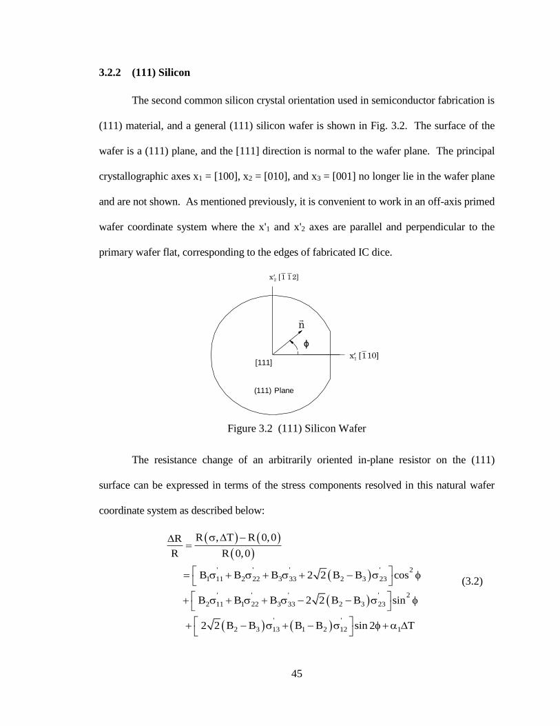
45
3.2.2 (111) Silicon
The second common silicon crystal orientation used in semiconductor fabrication is
(111) material, and a general (111) silicon wafer is shown in Fig. 3.2. The surface of the
wafer is a (111) plane, and the [111] direction is normal to the wafer plane. The principal
crystallographic axes x1 = [100], x2 = [010], and x3 = [001] no longer lie in the wafer plane
and are not shown. As mentioned previously, it is convenient to work in an off-axis primed
wafer coordinate system where the x'1 and x'2 axes are parallel and perpendicular to the
primary wafer flat, corresponding to the edges of fabricated IC dice.
Figure 3.2 (111) Silicon Wafer
The resistance change of an arbitrarily oriented in-plane resistor on the (111)
surface can be expressed in terms of the stress components resolved in this natural wafer
coordinate system as described below:
' ' ' ' 2
1 11 2 22 3 33 2 3 23
' ' ' ' 2
2 11 1 22 3 33 2 3 23
' '
2 3 13 1 2 12 1
R , T R 0,0R
R R 0,0
B B B 2 2 B B cos
B B B 2 2 B B sin
2 2 B B B B sin 2 T
f
f
f
(3.2)
f
[111]
(111) Plane
n
x1 110[ ]
x2 1 12[ ]
[111]
(111) Plane
ϕ

46
where the B coefficients are
3
2B
6
5B
2B 441211
3441211
2441211
1
and ϕ is the angle between the x'1-axis and the resistor orientation.
The B coefficients represent a set of linearly independent temperature dependent
combined parameters that are convenient for characterization of piezoresistance on the (111)
surface. These parameters must be measured before stress component values can be
extracted from resistance change measurements.
Typical values of the “B” coefficients for lightly doped material also appear in
Table 3.1. In n-type material, B1 and B2 are the largest coefficients whereas B3 is quite
small. One thing to be noted is that B1 and B2 are approximately equal in magnitude and
opposite in sign. For p-type material, B1 and B3 have the largest magnitudes, although all
three coefficients have useful values.
It is very important to note that the general resistance change expression in Eq. (3.2)
is dependent on all six of the stress components that describe the state of stress at a point in
the silicon material. Therefore, the potential exists for developing a sensor rosette that can
measure the complete three-dimensional state of stress at points on the surface of a die by
using properly designed (111) silicon sensors.
3.3 Rosette Designs
From Eq. (3.1), the resistance change of an in-plane sensor fabricated on (100)
silicon is observed to depend on four stress components (σ'11, σ'22, σ'33, σ'12) and the
orientation of the sensor element. Likewise, from Eq. (3.2), the resistance change of an
in-plane sensor fabricated on (111) silicon is found to depend upon all six stress

47
components and the orientation of the sensor. Because of this, it is natural to assume that
the potential exists to design a four-element rosette on (100) silicon capable of measuring
four stress components, and a six-element rosette on (111) silicon capable of measuring
all six stress components. However, it can also be proved theoretically that, when
considering all possible resistor orientations at a point, there are only three unique
(linearly independent) responses on any given silicon plane for a given silicon impurity
type.
The full potential of multi-element sensor rosettes to measure up to six stress
components can be achieved by using dual-polarity sensing elements fabricated with both
n-type and p-type silicon. Since the piezoresistive coefficients of the n-type and p-type
resistors are different, there can be up to six unique sensor responses in dual-polarity
rosettes.
Besides the ability to measure two additional stress components, theoretical
analysis has established that properly designed sensor rosettes on the (111) silicon wafer
plane have other advantages relative to sensors fabricated using standard (100) silicon
[88]. In particular, optimized sensors on (111) silicon are capable of measuring four
temperature compensated combined stress components, while those on (100) silicon can
only be used to measure two temperature compensated quantities.
In this discussion, "temperature compensated" refers to the ability to extract the
stress components directly from the resistance change measurements without the need to
know the temperature change ΔT. This is particularly important attribute, given the large
errors that can be introduced into non-temperature compensated stress sensor data when
the temperature change is not precisely known.

48
Furthermore, computer-aided symbolic analysis was used to consider all possible
silicon wafer orientations, and it established that the (111) plane in fact offers the
opportunity to measure the highest number (four) of stress components in a temperature
compensated manner of any possible silicon wafer plane[77, 78, 85, 89]. The four stress
components that can be measured in a temperature compensated manner are the three
shear stress components and the difference of the in plane normal stress components.
3.3.1 Optimized 4-Element Rosette on (100) Silicon
A four-element dual-polarity sensor rosette on (100) is shown in Fig. 3.3. The
rosette contains a 0-90o p-type resistor pair and a +45o n-type resistor pair. This choice of
sensor orientations minimizes thermally induced errors as well as those due to resistor
misalignment relative to the true crystallographic axes, and permits accurate temperature
compensated measurement of the values of the in-plane normal stress difference (σ'11 -
σ'22) and the in-plane shear stress σ'12 as outlined below.
Figure 3.3 A Four-Element Rosette for (100) Silicon
x [100]1
x [010]2
x« [110]1
x« [110]2
45
R1,p
R2,p
R4,nR3,n

49
Application of eq. (3.1) to the four resistor orientations gives the following relations
between the resistance changes and the stresses at the rosette site:
p p p p
S 44 S 44' ' p ' p111 22 12 33 1
1
p p p p
S 44 S 44' ' p ' p211 22 12 33 1
2
n' ' n ' n ' n3 S11 22 D 12 12 33 1
3
n' ' n ' n ' nS411 22 D 12 12 33 1
4
RT
R 2 2
RT
R 2 2
RT
R 2
RT
R 2
(3.3)
Six independent piezoresistive coefficients now appear, and superscripts n and p
are used to denote the piezoresistive coefficients of the n-type and p-type resistors,
respectively. The expressions in Eq. (3.3) can be inverted to yield Eqs. (3.4) for the four
stress components (σ'11, σ '22, σ '33, σ '12) in terms of the resistance changes of the sensing
elements, the six piezoresistive coefficients, and the temperature change ΔT.
2
2
1
1
p44
'22
'11
4
4
3
3
nD
12
n12
p11
p12
n11
n1
4
4
3
3pS
p1
2
2
1
1nS
33
2
2
1
1
p44
n12
p11
p12
n11
p1
2
2
1
1n12
n1
4
4
3
3p12
22
2
2
1
1
p44
n12
p11
p12
n11
p1
2
2
1
1n12
n1
4
4
3
3p12
11
R
R
R
R1
R
R -
R
R
2
1 =
) - 2(
T2R
R
R
R - T2
R
R
R
R
=
R
R -
R
R
2
1 -
) - 2(
T2R
R
R
R - T2
R
R
R
R
=
R
R -
R
R
2
1 +
) - 2(
T2R
R
R
R - T2
R
R
R
R
=
(3.4)
Direct combination of the expressions in eq. (3.4) also yields to two temperature
compensated (independent of ΔT) resistance-stress expressions.

50
The piezoresistive coefficients needed to solve for the stress components can be
measured using a combination of uniaxial and/or hydrostatic pressure calibration testing
[87-88]. The original choice of n- and p-type material for the four resistors in Fig. 3.3 is
based upon the values of p
44 andn
D in Table 3.1.
3.3.2 Optimized 8-Element Rosette on (111) Silicon
The eight-element dual-polarity rosette on (111) silicon illustrated in Fig. 3.4
contains p-type and n-type sensor sets, each with resistor elements making angles of ϕ = 0,
±45, and 90 degrees with respect to the horizontal x'1-axis. This sensor has been
developed for measurement of the complete state of stress at points on the surface of a
packaged semiconductor die. It has beenoptimized to measure four stress components in a
temperature compensated manner, and the “B” coefficients can be measured using a
combination of uniaxial and hydrostatic testing.
A six-element rosette (without the -45o resistors) can also be used to extract the
complete stress state. However, including the two extra resistors allows for more
convenient bridge measurements of the resistance changes and better stress measurement
localization as only 0/90o or +45o/-45o resistor pairs appear in any given expression.
Repeated application of Eq. (3.2) to each of the piezoresistive sensing elements
leads to the expressions in Eq. (3.5) for the stress-induced resistance changes. Superscripts
n and p are used on the combined piezoresistive coefficients to denote n-type and p-type
resistors, respectively. For an arbitrary state of stress, these expressions can be inverted to
solve for the six stress components in terms of the measured resistance changes, and the
results appear in Eq. (3.6).

51
T +)B B( )B - B(22 + B + ) + (2
B + B =
R
R
T +)B B(22 + B + B + B = R
R
n112
n2
n113
n3
n233
n32211
n2
n1
2
2
n123
n3
n233
n322
n211
n1
1
1
T +)B B( )B B(22 B+ ) + (2
B + B =
R
R
T +)B B(22 B + B + B = R
R
n112
n2
n113
n3
n233
n32211
n2
n1
4
4
n123
n3
n233
n322
n111
n2
3
3
(3.5)
T + )B B( )B B(22 B + ) + (2
B + B =
R
R
T +)B B(22 B + B + B = R
R
T + )B B( +)B B(22 + B + ) + (2
B + B =
R
R
T +)B B(22 + B + B + B = R
R
p112
p2
p113
p3
p233
p32211
p2
p1
8
8
p123
p3
p233
p322
p111
p2
7
7
p112
p2
p113
p3
p233
p32211
p2
p1
6
6
p123
p3
p233
p322
p211
p1
5
5
Figure 3.4 Top: A Sensor Rosette for (111) Silicon.
Bottom: Microphotograph of the Sensor Rosette
45
R4,n
R7,pR8,p
R1,n
R2,nR3,n
x [112]2
x [110]1
R6,p
R5,p
45

52
]B)B + B( B)B + B2[(
T2R
R
R
RB T2
R
R
R
RB
]B)B B( + B)B B( + B)B B2[(
R
R
R
R)B B(
R
R
R
R)B B(
= n3
p2
p1
p3
n2
n1
p1
7
7
5
5n3
n1
3
3
1
1p3
n1
p2
p3
n2
p3
p1
n3
p1
p2
7
7
5
5n2
n3
3
3
1
1p2
p3
11
]B)B + B( B)B + B2[(
T2R
R
R
RB T2
R
R
R
RB
]B)B B( + B)B B( + B)B B2[(
R
R
R
R)B B(
R
R
R
R)B B(
= n3
p2
p1
p3
n2
n1
p1
7
7
5
5n3
n1
3
3
1
1p3
n1
p2
p3
n2
p3
p1
n3
p1
p2
7
7
5
5n2
n3
3
3
1
1p2
p3
22
]B)B + B( B)B + B2[(
T2R
R
R
R)B + B( + T2
R
R
R
R)B + B(
= n3
p2
p1
p3
n2
n1
p1
7
7
5
5n2
n1
n1
3
3
1
1p2
p1
33
B)B B( + B)B B( + B)B B(
R
R
R
R )B B(
R
R
R
R)B B(
8
2 =
n1
p2
p3
n2
p3
p1
n3
p1
p2
6
6
8
8n1
n2
2
2
4
4p1
p2
13
(3.6)
B)B B( + B)B B( + B)B B(
R
R
R
R )B B( +
R
R
R
R )B B(
8
2 =
n1
p2
p3
n2
p3
p1
n3
p1
p2
7
7
5
5n1
n2
3
3
1
1p1
p2
23
]B)B B( + B)B B( + B)B B2[(
R
R
R
R )B B( +
R
R
R
R )B B(
= n1
p2
p3
n2
p3
p1
n3
p1
p2
6
6
8
8n2
n3
2
2
4
4p2
p3
12
]B)B B( + B)B B( + B)B B[(
R
R
R
R )B B(
R
R
R
R )B B(
= n1
p2
p3
n2
p3
p1
n3
p1
p2
7
7
5
5n2
n3
3
3
1
1p2
p3
2211
In Eq. (3.5) and (3.6), only the first order temperature terms have been retained.
From the expressions in Eq. (3.6), it is clear that the extraction of the three shear stresses
(σ'13, σ'23, and σ '12) from the measured resistance changes is independent of T. Evaluation
of the three normal stress components requires measurement of the normalized resistance
changes of the sensors and the temperature change ΔT experienced by the sensing elements.
The temperature coefficients of resistance must also be known for each doping type.
Besides the three shear stresses, an additional temperature compensated quantity can be
obtained by subtracting the expressions for the normal stresses σ '11 and σ '22.

53
3.4 Stress Extraction using Piezoresistive Theory
A typical expression of the relation between resistor sensor response and applied
stress is shown in eq. (3.7).
Silicon)100(for
R
R -
R
R
2
1 +
) - 2(
T2R
R
R
R - T2
R
R
R
R
= 2
2
1
1
p44
n12
p11
p12
n11
p1
2
2
1
1n12
n1
4
4
3
3p12
11
(3.7)
Silicon)111(for
]B)B + B( B)B + B2[(
T2R
R
R
R)B + B( + T2
R
R
R
R)B + B(
= n3
p2
p1
p3
n2
n1
p1
7
7
5
5n2
n1
n1
3
3
1
1p2
p1
33
These mathematical expressions in Eq. (3.8) indicate that to extract stress using
the piezoresistive stress sensors either on (100) or (111) silicon, the piezoresistive
coefficients ‘π’ for (100) and ‘B’ for (111) silicon, temperature change ‘ΔT’ and the
change in resistance value of the resistors ‘ΔR/R’ need to be measured. To obtain the
piezoresistive coefficients, a calibration procedure is performed before stress component
values can be extracted. The calibration of the piezoresistive coefficient values are done
using methods such as four-point bending, cantilever bending, and hydrostatic pressure.
3.5 Sensitivity Analysis
In order to extract die stresses using piezoresistive sensor rosette, resistance
changes of the sensing elements, piezoresistive coefficients and temperature are required to
be measured as can be seen from Eqs. (3.5) and (3.7). The resistance change of the sensing
elements are obtained from the deviation of the resistance values of the sensors from their

54
initial values. The piezoresistive coefficient values are measured using methods including
four-point bending, cantilever bending, and hydrostatic pressure. Each of the measurement
techniques inherently introduces experimental error. Errors in the experiment or the
uncertainty in the experiments can be due to the methodology, operational condition, and
environmental effect or due to the problematic measurement unit. Other sources of
uncertainty include the precise surface orientation, location of the actual crystallographic
axes, and precision of mask alignment during semiconductor fabrication[79].
Experimental uncertainty inherently introduces errors in the measured values of
the resistance changes and temperature. The calibration process of the piezoresistive
coefficients results in uncertainties of 10% or more in the values of the piezoresistive
coefficients used to calculate the stresses from measured resistor changes. These
uncertainties can potentially lead to significant errors in the extracted stress values. So it
is important to express the measured calibration coefficients, temperatures and resistance
change values by including the associated uncertainties in the measurements. These
uncertainties of the extracted stress data due to the uncertainties in the input parameters
can be evaluated by data analysis technique, predominantly statistical technique.
The uncertainties in the extracted outcome of an experiment because of the
uncertainties or errors in the input parameters can be addressed using sensitivity analysis.
The sensitivity analysis is an effective way to estimate the uncertainties of an extracted or
derived quantity by accounting for the different uncertainties in the experimentally
measured input parameters to obtain the response.
To explore how the uncertainties in the input parameters affect the response, we
use the classic definition of sensitivity of a given quantity to parametric changes. If an

55
algebraic equation exists to define the correlation between the output response and the
input variables, then the sensitivity of an intended response can be calculated from the
first order partial derivative of the response to the given input variables. For example, the
sensitivity of stress component σ'ij to changes in a given parameter P is given by
P
P
P
PS
ij
ijij
ij
ijP (3.8)
ijPS
is a unit-less quantity that represents the ratio of the fractional change in stress that
results from a fractional change in the specified parameter. The quotient (P/ ij )is
introduced to remove the effect of units by normalizing the parameters. The sensitivity of
an output to its input value demonstrate how significant is the input variability. The larger
the sensitivity value, the more significant is the input value. Values of S equal to one or
less are regarded as good, whereas those much greater than one are problematic.
3.5.1 Resistance Measurement Errors
A typical resistor sensitivity expression for (111) silicon (1 of a total of 63)
resulting from the evaluation of Eq. (3.8) using the results in equations in Eq. (3.6)
appears in Eq. (3.9).
'33
'23n
3n2
n3'
33
'22n
2'33
'11n
1
n3
p2
p1
p3
n2
n1
p2
p1
'33
1R
1R
)BB(22BBB
]B)BB(B)BB[(2
)BB(S
(3.9)
As an example, this expression indicates the problem of having a small stress
σ'33in the denominator of the expression that will cause the sensitivity to be high.

56
Therefore, it is difficult to measure a small stress such as σ'33 in the presence of large
normal stresses. However, one must be careful with the sensitivities. A zero value of
stress leads to an infinite sensitivity, and it is also useful to study the individual
derivatives of stress with respect to the resistor values that are needed to evaluate Eq.
(3.9). For example, the derivative of σ'33 with respect to R1 is
1
1
33
11
33
n1
p2
p3
n2
p3
p1
n3
p1
p2
p2
p1
1
1
33
R
R0,0R
1
R and
]B)BB(B)BB(B)BB[(2
)BB(
R
R
(3.10)
The complete set of expressions for the derivatives appears in Table B.1 of
Appendix B. Note that these expressions are convenient since they are independent of
stress, which is not the case for the derivatives related to the piezoresistive coefficients.
3.5.2 Temperature Measurement Errors
In a similar manner, the sensitivity of stress to temperature is evaluated as
T
TS
ij
ij
ijT
(3.11)
A sample of the derivative needed above is
n1
p2
p3
n2
p3
p1
n3
p1
p2
p3
n1
n3
p111
B)BB(B)BB(B)BB(
BB
T
(3.12)
The derivatives for the three temperature dependent stresses appear in Table B.2
of Appendix B.

57
3.5.3 Piezoresistive Coefficient Uncertainty
The sensitivity of stress σ to changes in values of the π or B coefficients is expressed
using (3.8) as
k
k
ij
ij
k
ij
ij
kij
kBB
B
B
BS (3.13)
A sample of the derivative needed above is
)1(]B)BB(B)BB[(2
BB
)1(]B)BB(B)BB(B)BB[(2
)BB(BS
'11
'22
n3
p2
p1
p3
n2
n1
n3
p1
'11
'22
n1
p2
p3
n2
p3
p1
n3
p1
p2
n3
n2
p1
'11p1
B
(3.14)
The complexity of the interaction between stress and B coefficient variation is
apparent in (3.14) and is hard to interpret, so the sensitivities have been investigated
through numerical evaluation in the following sections. The complete set of stress
sensitivities to piezoresistive coefficients appear in Appendix C.
In the following part of this chapter the uncertainties of the piezoresistive
coefficients are discussed and then the discussion is extended to error analysis in order to
include the sensitivities of the extracted stresses to errors in the measurement of the
sensor resistances and temperature. Monte-Carlo simulation results yield estimates for
errors due to uncertainty in sensor element measurements.
Sensitivity results are generated across the surface of a flip-chip die based upon
finite-element simulation for a generic flip chip package configuration. The results are
presented in two- and three-dimensional graphical form and demonstrate that the
sensitivities are stress dependent and again vary widely from very small to very large
over the die surface.

58
3.6 Finite Element Modeling
The finite element modeling of a flip chip package is performed in order to obtain
the die stress distribution of a typical flip chip assembly. The die stress data from the
finite element simulation was further used to calculate the sensitivity of the the
piezoresistive coefficients to the extracted stress values. A drawing of the basic flip chip
package to be modeled here appears in Fig. 3.5.
The simplified finite element model includes a 51 mm x 51 mm ceramic substrate,
the 20 mm x 20 mm sensor die, and the under fill including its fillet. ANSYS® was used
to obtain the stress distribution over the surface of the die resulting from cooling the die
from its assumed stress-free state at 150oC to the room temperature of 25oC. The model
assumed anisotropic and elastic properties for silicon, elastic properties for the ceramic,
and temperature dependent elastic-plastic behavior for the under-fill material.
Figure 3.5 Flip-Chip Package and the Finite-Element Model
Sensors
Lid
Ceramic Substrate
TIM1Lid Attachment Adhesive
Sensors
Lid
Ceramic Substrate
TIM1Lid Attachment Adhesive
1
XY
Z
ANSYS 11.0
MAR 6 2009
16:24:42
ELEMENTS
MAT NUM
1
ANSYS 11.0
MAR 6 2009
16:27:23
ELEMENTS
MAT NUM

59
The resulting stress distributions appear in Figs. 3.6-3.8. For clarity in viewing the
results of both the stress distributions and the stress sensitivity results, the data from the
FEM simulations have been transferred to MATLAB for graphical presentation in both
2D contour plots and 3D surface plots. The finite element stress predictions can be
combined with the analytical sensitivity formulas to generate plots of the sensitivities
over the die surface.
Figure 3.6 Simulation Results for '11.
. Table 3.2 presents measured values of the piezoresistive coefficients utilized in the
sensitivity calculations, and sample results are presented in Figs. 3.9-3.12.
Table 3.2 Typical Coefficient Data (oC, 1/TPa, ppm/oC)
T n1B n
2B n3B
p1B
p2B
p3B
p1 n
1
300 -230 207 55 507 -145 -399 1800 2800
Sigma11
0
30
60
90
A MATLAB Code was written to Extract
and Transfer the Stress Values for the
Sensitivity Calculations.
(MPa)11
(MPa)11
1
MN
MX X
Y
Z
-100
-90
-80
-70
-60
-50
-40
-30
-20
-10
ANSYS 11.0
MAR 6 2009
18:52:35
NODAL SOLUTION
STEP=1
SUB =1
TIME=400
SX (AVG)
RSYS=0
DMX =.104401
SMN =-91.681
SMX =-5.267

60
3.7 Discussion of Results
In Fig. 3.7, we observe that the in-plane normal stresses, '11 and '22, are large in
the center of the die, and tail off toward the edges of the die. The stress normal to the
surface, '33, is low over most of the die, but becomes large at the four corners since the
die is being warped yielding high out-of-plane stress at the corners. In Fig. 3.8, one
observes concentrations of all three shear stresses in the vicinity of the corners. Thus
there are large variations of all the individual stresses across the die surface, which will
lead to significant variations of the stress sensitivities as well.
Figure 3.7 Simulated Normal Stress Fields on the Die Surface
3.7.1 Review of Piezoresistive Coefficient Sensitivities
Graphs of selected plots of the stress sensitivities appear in Figs. 3.9 - 3.12. High
sensitivity suggests regions where errors will most likely occur during measurements. A
sensitivity of 10 indicates that a 10% error in a coefficient leads to a 100% error in the
(MPa)11 (MPa)22 (MPa)33 sigma33
0
5
10
15
(MPa)11 (MPa)22 (MPa)33
Sigma11
0
20
40
60
80
Sigma22
0
20
40
60
80

61
stress estimate, so small sensitivities are most desirable. Sensitivities of less than 2 or so
are acceptable, whereas those above 5 are becoming problematic.
Figure 3.8 Shear Stress Fields Across the Die
In Fig. 3.9, we find sensitivities of '11 to n2
n1 B and B ranging from 5 to 15 that
should raise a flag. A similar result occurs in Fig. 3.10 for '22. We must expect relatively
wide data spreads and error bars for in-plane normal stress measurements. From Fig.
3.9(c), we see a small sensitivity to the n3B coefficient across the whole die. This is
encouraging because measurement of the small n3B is quite difficult and has many
sources of possible error.
sigma12
0
10
20
30
(MPa)12
(MPa)12
sigma13
0
5
10
15
20
(MPa)13
(MPa)13
1x
2x
1x
2x
sigma23
0
2
4
6
8
10
(MPa)23
(MPa)23
1x
2x

62
Figure 3.9 Sample Sensitivities of the In-Plane Normal Stress
σ'11 to Errors in Various B Parameters
Figure 3.10 Sample Sensitivities of the In-Plane Normal Stresses
σ'11 and σ'22 to Errors in B Parameters.
11 Sensitivity to B2
n
Sensitivity of s igma11 on bn2
0
5
10
15
11 Sensitivity to B3
n
Sensitivity of sigma11 on bn3
0
0.1
0.2
0.3
0.4
0.5
1x
2x
1x
2x
Sensitivity of sigma11 on bn1
0
5
10
15
11 Sensitivity toB1
n
1x
2x
σ'11Sensitivity to σ'11Sensitivity to σ'11Sensitivity to n
1Bn
2Bn
3B
1x
2x
11 Sensitivity to B1
p
22 Sensitivity to B1
n
Sensitivity of sigma11 on bn1
0
5
10
15
1x
2x
1x
2x
Sensitivity of sigma22 on bp1
2
2.5
3
3.5
4
22 Sensitivity to B1
pσ'11 Sensitivity to B1
p σ'22 Sensitivity to B1
𝑛 σ'22 Sensitivity to B1𝑝

63
Figure 3.11 Sensitivity of Shear Stresses (Temperature Compensated)
to Errors in Various B Parameters.
Figure 3.12 Sensitivity of Shear Stresses (Temperature Compensated)
to Errors in Various B Parameters.
13 Sensitivity to B3
n
12 Sensitivity toB1
n
12 Sensitivity to B1
p
13 Sensitivity toB3
p
σ'12 Sensitivity to B1p σ'13 Sensitivity to B3
p
σ'12 Sensitivity to B1n σ'13 Sensitivity to B3
n
( 11 22 ) Sensitivity toB1
n
23 Sensitivity toB3
n
23 Sensitivity to B3
p
( 11 22 ) SensitivitytoB1
p
σ'23 Sensitivity to B3n
σ'23 Sensitivity to B3𝑝
(σ'11- σ'22) Sensitivity to B1n
(σ'11- σ'22) Sensitivity to B1𝑝

64
Figure 3.13 Fractional Errors for In-Plane Normal Stresses to a 5˚K
Temperature Error at 300 K Showing High Sensitivity Across the Die.
The sensitivities in the first and third parts of Figure 3.10 are mostly between 2
and 4 and are relatively low, whereas those in the second part are relatively large. Figure
3.11 and 3.12 presents samples of the sensitivities to piezoresistive coefficient variation
for the temperature compensated stresses that can be measured using the (111) rosettes.
Here we observe very low sensitivities across the whole die for each case.
Figure 3.13 shows the high sensitivity of the in-plane normal stresses to
temperature measurement errors, another indicator of the importance of strict control of
temperature and other errors that may mimic temperature errors [79, 81].
Table 3.3 presents complete sets of calculations of the sensitivities at two points
on the surface of the die, one at the die center (3.3-A) and one at the center of the edge of
the die (3.3-B).. For the cases highlighted in italics (and green) in Table 3.3 A and 3.3 B,
Fractional Error in σʹ11 Fractional Error in σʹ22

65
the sensitivities are small, whereas those in bold (and yellow) range from not good to
terrible.
Table 3.3 Stress Sensitivities with respect to Errors in the “B” Coefficients and
Temperature
Table 3.3 A- Magnitudes Near Die Center
n1B n
2B n3B p
1B p2B
p3B T
σ'11 8.54 7.70 0.00 2.60 0.74 0.00 373
σ'22 8.54 7.70 0.00 2.60 0.74 0.00 373
σ'33 253000 228000 1.86 35400 10100 0.85 107
σ'12 0.28 0.34 0.02 0.37 0.14 0.10 0
σ'23 4.47 3.38 0.17 6.61 1.59 0.83 0
σ'13 2.06 2.49 0.17 3.04 1.17 0.83 0
σ'11- σ'22 0.28 0.21 0.01 0.37 0.09 0.05 0
σ'11+ σ'22 8.55 7.69 0.00 2.60 0.74 0.00 373
Table 3.3 B - Magnitudes Near Center of Die Edge
σ'11 5.85 4.91 0.00 1.91 0.47 0.00 469
σ'22 15.5 13.9 0.04 4.36 1.29 0.09 1210
σ'33 1920 1730 1.86 269 76.8 0.86 145000
σ'12 0.28 5.39 1.37 0.37 2.26 5.93 0
σ'23 1.52 2.01 0.17 2.25 0.94 0.83 0
σ'13 0.03 0.67 0.17 0.05 0.32 0.83 0
σ'11- σ'22 0.28 0.37 0.03 0.37 0.15 0.14 0
σ'11+ σ'22 8.55 7.70 0.01 2.60 0.74 0.01 676
. A couple of observations can be made from Table 3.3 A. For example, the
sensitivities of σ'11 and σ'22 to B1n is 8.54 which indicates that a 10% error in B1
n can lead
to 85% error in the calculated values of σ'11 and σ'22. The high sensitivities to temperature
in the individual normal stresses are also evident. A very high sensitivities were noted for
'33, which is very small at the middle of the die. Therefore, the sensitivity data indicates
that the measurement of '33is very difficult. The sensitivities of the temperature

66
compensated stresses to the piezoresistive coefficients in general show lower sensitivities.
A number of the sensitivities are large even in the case of the temperature compensated
shear stresses especially for σ'23 and σ'13.
A second case that is representative of the stress in the middle of one side of the
die appears in Table 3.3 B. Here, only a 1% error in B1n or B1
pmay lead to significant
errors in σ'22 and σ'33. The high sensitivities to B1n orB1
parise because, for typical values,
they nearly cancel each other in the denominator of the sensitivity expression. These
high sensitivities are a further argument for making temperature compensated
measurements whenever possible. Tables 3.3 A and 3.3 B both indicate there will be
difficulty in obtaining accurate values for σ'33.
Coefficients B3n or B3
𝑝 are the most difficult to measure accurately, requiring the
use of hydrostatic pressure or some other technique. Fortunately, the sensitivities to
errors in these coefficients are all relatively small. Note that the very high sensitivities to
temperature have been discussed in references [79, 81]. One must be careful when using
sensitivities as we can observe from those for σ'33. Sensitivity S can become large when a
stress is small since σ'33 is used as a normalization factor. The results further indicate the
difficulty of measuring small stresses in region in which other stresses are large. This
problem can also be inferred from the resistance change equations.
Since all the B parameters will be in error, the sum of the magnitudes of a given
row is also significant. Using the chain rule,
k k
kij
kBk
k
k
ij
ijij
ij
B
BSB
B
1 (3.15)

67
Table 3.4 presents the results of a worst - case evaluation of Eq. (3.15) by
summing the magnitudes of the results assuming a 5% error in each coefficient and a 1-K
temperature error at T = 300 K. Here we see that significant percentage errors can occur
in extraction of all the stresses due to parameter uncertainty. The best case is that the
temperature compensated in-plane terms, (σ'11- σ'22) and σ'12.
Table 3.4 Fractional Error - Worst Case Total
Stress Die Center Die Edge
σ'11 2.2 2.2
σ'22 2.2 5.8
σ'33 61400 682
σ'12 0.1 0.8
σ'23 0.9 0.4
σ'13 0.05 0.1
σ'11- σ'22 0.1 0.1
σ'11+ σ'22 2.2 3.2
ΔB/B = 0.05 and ΔT/T = 1/300
3.7.2 Sensitivities to Temperature Measurement Errors
The values for the derivatives of the normal stresses ('11, '22, '33) with respect
to temperature appear in Table 3.5. The values are on the order of 100 MPa/oC! Thus, a
0.1 degree error in measuring temperature will make a 10 MPa error in the stress
extraction. The other stresses are temperature compensated and have zero derivatives.
3.7.3 Sensitivities to Resistor Measurement Errors
Values for the derivatives of stress with respect to resistor values expressed in
MPa/% appear in Table 3.6 based upon the data in Table 3.1. The values for the

68
temperature dependent stress extractions are high, whereas those for the temperature-
compensated calculations are low. For example, a 1% measurement error in R1 causes a
180 MPa error in the extracted value of '11. These derivatives are used in the Monte
Carlo analysis in the next section.
Table 3.5 Derivatives with Respect to Temperature
00
00
00
00
7.93D
BBBB
113D
BB
113D
BB
C)(MPa/ ValueT
2211
12
23
13
2
n2
n1
p1
p2
p1
n1
33
2
n3
p1
p3
n1
22
2
n3
p1
p3
n1
11
o
Table 3.6 Derivatives of Stress with Respect to Errors in Measured Resistor Values
ij
k kR R
(MPa/%)
R1 R2 R3 R4 R5 R6 R7 R8
σ'11 180 0 192 0 29.2 0 22.0 0
σ'22 192 0 180 0 22.0 0 29.2 0
σ'33 -8.61 0 -8.61 0 10.7 0 10.7 0
σ'12 0 5.49 0 -5.49 0 3.68 0 -3.68
σ'23 5.49 0 5.49 0 3.68 0 -3.68 0
σ'13 0 -6.04 0 6.04 0 3.62 0 -3.62
σ'11- σ'22 -12.1 0 12.1 0 7.23 0 -7.23 0
σ'11+ σ'22 372 0 372 0 51.2 0 51.2 0

69
Figure 3.14 Sample Sensitivities of σ'11 with respect to Errors in
(a) ΔR1/R1 (b) ΔR3/R3 (c) ΔR5/R5 (d) ΔR7/R7
Figure 3.15 Sample Sensitivities of σ'22 with respect to Errors in
(a) ΔR1/R1 (b) ΔR3/R3 (c) ΔR5/R5 (d) ΔR7/R7
(a) (b)
(c) (d)
(a) (b)
(c) (d)

70
Examples of the sensitivities to resistor measurement error are plotted in Figs.
3.14-3.15 using expressions similar to Eq. (3.10) and the simulated stress distributions.
These results are similar to those for the piezoresistive coefficients and exhibit wide
variation across the wafer and from stress to stress. The sensitivity of '11 with respect to
R3 is a problem along the edges where '11 is small. Similarly, the sensitivity of '22 with
respect to R1 is a problem along the edges where '22 is small.
3.7.4 Monte Carlo Analysis
Monte Carlo analysis is an experimental probabilistic method for determining the
sensitivity of a system by considering the variables that effect that system within
statistical limits of those variables. In an experiment, some of the parameters that
determine the data of the experiment can contain uncertainties in their values and their
values can be distributed within their maximum and minimum limit. In such case it is
highly unlikely for all the parameters of an experiment to reach their maximum
uncertainty limit at the same time and vice versa. The analysis based on all randomly
varying parameters attaining the extremes at the same time is referred to as worst- case
analysis technique and this technique often results in conservative analysis of the
experimental result and that may prove to be expensive due to the overestimation of the
parameters of the experiment. Another way of dealing with experiments with randomly
distributed parameters is a statistical method referred to as Monte Carlo analysis which is
quite complex but yield in a satisfactory result. During dealing with uncertainties of the
parameters in data estimation, random values of the parameters are used in the analysis
within their uncertainty space instead of a single calculation that is performed in straight

71
forward methods. Such analysis yields closer approximation of the measurement data that
are probabilistic in nature.
The way the analysis works is that it uses random values of each of the
parameters of an experiment which is selected from the possible distributions of
parameters to statistically predict the behavior of the experiment. Multiple cases of such
prediction of the experiment are generated by random selection of its parameters and a
probabilistic nature of the experiment is established from the analysis of several test
cases. Usually a computer program is generated to carry on the Monte Carlo simulation
capable of generating random numbers for the parameters. The flowchart of the Monte
Carlo analysis is shown in Fig 3.16.
For calculation of overall uncertainty, the errors associated with all the variables
of an experiment are needed to be specified. An error is usually expressed by a
probability distribution function or by its mean value and its standard deviation. We can
obtain additional insight into the expected errors caused by imprecise resistor
measurement by using Monte Carlo analysis to estimate the errors in stress extraction
caused by various levels of uncertainty in the measured values of the resistances. Using
the chain rule,
)0,0(R
R
R
RR
R i
i8
1
i
i
ij
i
8
1 i
ij
ij
(3.16)
For the Monte Carlo simulation, the factional errors in the resistor values are
chosen randomly assuming uniformly distributed values. In our experiments, we have
observed maximum deviations of approximately 0.05% in the resistor measurements

72
with 6 digit multi-meters, and these have been used in the uniform random value
generation. The results appear in Table 3.7 for a small 100-case simulation.
Figure 3.16 Monte Carlo Process Steps
The averages are small as they should be since the random resistor values have
zero mean. The standard deviations for the temperature compensated stresses are a
fraction of 1 MPa with maximum and minimum values a factor of two larger. The non-
]B)BB(B)BB(B)BB[(2
R
R
R
R)BB(
R
R
R
R)BB(
n1
p2
p3
n2
p3
p1
n3
p1
p2
6
6
8
8n2
n3
2
2
4
4p2
p3
12
An example stress
expression
Extracted Stress Value Depends on the Resistance
Change Measurements
Monte Carlo
Simulation
The ΔR/R Values are Randomly Selected from
Uniform Distribution of these Parameters.
The Particular Stress is Calculated using
Randomly Selected ΔR/R Values
Similar Calculations done for Different set of
Randomly Selected Values for Several cases
Randomly Selected ΔR/R Values
Statistical Behavior of the Stress Generated
from the Analysis of Several test cases
Randomly Selected ΔR/R Values 0

73
temperature compensated stress have much higher sensitivities, and these result in larger
errors in '11 and '22. However, since these two in-plane stresses are often relatively large
(100 MPa and greater), the errors are still not severe. Based upon these results, it appears
that errors due to resistor measurement errors are entirely manageable.
Table 3.7 Monte Carlo Results 100 Cases (MPa)
σ'11- σ'22 σ'12 σ'23 σ'13 σ'11 σ'22 σ'33
Average 0.0025 0.0068 0.029 0.014 0.53 0.035 0.035
St. Dev. 0.60 0.30 0.28 0.28 7.8 7.9 0.54
Minimum -1.3 -0.69 -0.62 -0.50 -17 -16 -1.4
Maximum 1.2 0.74 0.68 0.67 17 16 1.4
3.8 Summary and Discussion
Multi-element resistor rosettes on silicon are widely utilized to measure integrated
circuit die stress in electronic packages and other applications. Previous analyses of many
sources of error have led to rosette optimization and the realization that temperature
compensated stress extraction should be used whenever possible. This chapter has
discussed the errors that occur in stress extraction due to the inherent uncertainty in
knowledge of the values of the piezoresistive coefficients as well as measurement errors
associated with measurement of rosette resistor values and temperature for stresses
corresponding to a die in a flip chip package.
Expressions for the sensitivity of extracted stress to resistor measurement,
temperature measurement and piezoresistance coefficient measurement errors have been
presented and discussed. Monte Carlo simulations have been utilized to estimate the
expected errors in stress measurements of a silicon die mounted in a typical flip chip
package due to the resistance measurement error. The results presented here show the

74
sensitivities to be stress dependent and to vary widely over the die surface and that the
temperature compensated stress terms generally tend to have low sensitivity to
measurement uncertainty, although this is not true for every case. Therefore, further
studies must be directed towards optimizing the multi-element sensor rosette (111) silicon
to have lower sensitivities to the piezoresistance coefficient, temperature and resistance
change value uncertainties.
.

75
CHAPTER 4
CURRENT DEPENDENCE OF THE PIEZORESISTIVE COEFFICIENTS OF
MOSFETS ON (100) SILICON
4.1 Introduction
Piezoresistive stress sensors are widely used to monitor mechanical stresses
developed on the chip and to package during its operation. These sensors offer non-
intrusive and real time measurement of stresses, and they can be fabricated on the chip
using the prevailing microelectronic fabrication technology. Because of the advantage of
measuring stress on a chip in packaged condition, it has been successfully utilized to
monitor chip and package health and reliability over period of time. Implanted or diffused
resistor sensors are most prevalent stress sensors which are fabricated at suitable
locations on the surface of the die. These sensors are not mounted like traditional strain
gauges rather they are fabricated on the surface of the die, hence an integral part of the
die. The problems associated with resistor sensors are that they occupy large area in the
chip in order to have reasonable resistor values. As a result, they cannot provide localized
stress value and can only provide an average stress distribution over the area of the sensor.
These sensors are often highly doped which causes low sensitivity of these devices.
Metal-oxide-semiconductor (MOS) transistors on (100) silicon are excellent stress
sensors because of their advantages of smaller size, high sensitivity due to lighter doping,
operable in wide temperature range over the traditional resistor sensors. The resistive

76
channel of the MOS transistor can be utilized as piezoresistive element. They can be used
as sensor arrays that can provide high-resolution mapping of stress across the surface of
specially designed test die [88, 130, 195]. Optimized piezoresistive FET (PiFET) rosettes
on (100) silicon make use of the two largest piezoresistive coefficients (pi-coefficients),
p44 of PMOS devices and
nD of NMOS devices, to measure the in-plane normal stress
difference )( 2211 and the in-plane shear stress12 on the surface of the silicon
wafer, thereby providing highly localized stress measurements with high sensitivity[129].
However, the MOS pi-coefficients of the sensor rosettes have typically been evaluated at
only one operating point without any real data to guide the choice of operating conditions.
This chapter presents new results for the operating point dependence of the
piezoresistive coefficients of PMOS and NMOS devices. Uniaxial stress is utilized to
calibrate both the normal stress difference and shear stress sensors, and the piezoresistive
coefficient values are characterized as a function of drain current thereby providing the
information necessary to make appropriate operating point choices for the design of
CMOS stress sensors. From a more fundamental point of view, it is shown that the
magnitude of thep44 exhibits a direct correlation with the PMOS channel mobility,
whereas nD exhibits a nonlinear relation to NMOS channel mobility.
4.2 Metal Oxide Semiconductor Transistors
This section contains an overview of a metal oxide semiconductor field effect
transistor (MOSFET). It is the most widely used device in IC circuits. Fig. 4.1 shows a
schematic structure of two types of MOSFETs; NMOS and PMOS. As the figure
indicates, this transistor consists of diffused or implanted regions of source and drain, an

77
SiO2 insulator, a channel region and a gate. The source and the drain as the names
indicate are the sources of the electrons/holes and provides a drain for those carriers
respectively. The gate is insulated from the silicon substrate by a high quality insulator
usually SiO2. The surface potential of the silicon is determined by the gate voltage and by
applying proper gate voltage, an inversion layer can be created in the region between
source and drain with an electric field through the gate oxide that determines the
conduction through the transistor. Based on operation of these transistors at zero gate-
source voltage, they can be classified as either depletion-mode or enhancement-mode
transistors. In depletion-mode device, at zero gate voltage the device is in the ON state
and in enhancement-mode device the transistor is OFF at zero gate voltage. Depletion-
mode devices contain an conductive channel region which can be depleted through an
application of a gate voltage. Enhancement-mode devices do not contain a built in
channel, rather conduction of carriers occur by developing a channel region by applying
an appropriate gate voltage. Most silicon transistors are enhancement-mode transistors.
Figure 4.1 Schematic Diagram of an NMOS (left) and PMOS (right) Transistors
The threshold voltage, VT of a transistor corresponds to the minimum gate-source
voltage VGS that is required to generate conduction of carriers from the source to drain
n+ n+
Source Drain
Gate
Gate
Oxide
Channel
p type substrate
p+
Source Drain
Gate
Gate
Oxide
Channel p+
n type substrate

78
terminals. For an enhancement mode FET, depending upon the voltages at the terminals,
there are three different operational regions, cutoff, linear and saturation regions. These
three different operation mode are discussed in the following:
Cutoff Region:
The cutoff region occurs when the gate-source voltage VGS is less than the
threshold voltage VT. In this operation mode only a small leakage current flows through
the device and the transistor is basically considered to be turned off.
Linear Region:
The linear region of the transistor is entered when the gate-source voltage is
above threshold voltage (VGS> VT) but still below the value required for saturation, that is
(VGS -VT)>VDS, where VDS is drain–source voltage. In this region the transistor is turned
on and a charge rich inversion layer is formed between the source and drain terminals
that allows conduction of current between the source and drain. If the drain to source
voltage is increased by a small amount, the conducting current will increase linearly. In
linear region the transistor acts as a variable resistor which is modulated by the gate
voltage. The drain current in the linear region is expressed as:
DSDN n GS TN DS
SDDP p GS TP SD
VI K V V V for NMOS
2
Vand I K V V V for PMOS
2
(4.1)
where Kn and Kp are the transconduction parameters defined as
ox
n
ox
WK
T L
(4.2)

79
where VTN and VTP are the NMOS and PMOS threshold voltages of the transistor, μn
and μp are the electron mobility and hole mobility respectively, Tox is the oxide
thickness,εox is the dielectric constant of the oxide layer and W and L are the width and
length of the channel, respectively.
Saturation (Pinch Off) Region.
The transistor operates in the saturation region when the drain voltage exceeds the
saturation voltage that is VDS ≥(VGS -VT). The increase of drain voltage causes the
depletion region from the surrounding to make the channel near the drain to narrow down
and that will cause reduction of charge carrier density. As the drain current increases, the
channel will be totally “pinched off” from the drain region indicating lack of channel
region near the drain. However, the current through the device will still continue to
conduct even with the pinch off because the high electric field between the drain and the
channel causes charges to be swept through the depletion region into the drain. In the
saturation region, the DC drain current has a weak dependence on drain voltage and is
modulated predominantly by the gate-source voltage. The expression for drain current in
the saturation region can be expressed as:
2nDN GS TN n DS
2p
DP GS TP p SD
KI V V (1 V ) for NMOS
2
Kand I V V (1 V ) for PMOS
2
(4.3)
where n
and p
are the channel length modulation parameters that model the current
dependence on the drain voltage.

80
4.3 Piezoresistive MOS Sensors
The theory of piezoresistance effect in MOSFETs that describes the relation
between transistor response and applied stress is explained in Appendix A. The
conduction of the carriers through the channel determined by the resistive region of the
channel when the transistor is operated in strong inversion in either linear or saturation
region. The normalized change in drain current due to stress for a MOSFET on (100)
silicon in strong inversion can be written [134] as
)T(f2sin
sin22
cos22I
I
12D3312
222
44S11
44S
222
44S11
44S
D
D
f
f
f
(4.4)
Conceptual layouts of the optimized PMOS and NMOS stress sensor rosettes [130,
134] appear in Fig. 4.2 where the (0-90o) PMOS transistor pair measures the difference in
the in-plane normal stresses (σʹ11-σʹ22), and the (±45o) NMOS pair measures in-plane
shear stress . The stresses are resolved along the xʹ1andxʹ2axes defined for the (001)
silicon wafer in Fig. 4.3.
Figure 4.2 Conceptual Layouts of 0/90o PMOS and ±45o NMOS
Stress Sensors on (100) Silicon
¢s12

81
Figure 4.3 (001) Silicon Wafer Coordinates
The stated angles indicate the channel orientation relative to the [110] wafer axis.
Stresses and pi-coefficients are both determined from fractional changes in the pairs of
drain currents for the circuits in Fig. 4.4, assuming saturation region operation:
p90 044 11 22
90 0
n n45 45D 12 S 12
45 45
I Ifor PMOS
I I
I I2 6 for NMOS
I I
(4.5)
These circuits provide differential measurements, so transistor temperature
dependencies cancel out in these expressions. As mentioned in the introduction, the
PMOS and NMOS transistor pairs in the “optimized” FET rosettes are chosen totake
advantage of the largest piezoresistive coefficients based upon the classic values for bulk
silicon in Table 4.1.
Figure 4.4 PMOS (left) & NMOS (right) Sensor Circuits
f
[111]
(111) Plane
n
x1 110[ ]
x2 1 12[ ]
[100]
(100) Plane
ϕ
1x [010]2x [110]
1x [110]
I90
I0
M1
M2VSG
VDD
VGS
I-45 I45
+
-

82
Table 4.1 Classic Piezoresistive Coefficients for Lightly-
Doped Silicon from C. S. Smith [23]
Coefficient n-type Si
(1/TPa)
p-type Si
(1/TPa)
π11
-1020 +66
π 12
+534 -11
π 44
-136 +1380
πS= π11+ π22
-488 +55
πD = π11- π22
-1560 +77
It can be observed from (4.5) thatp44 is easily determined by applying a
controlled uniaxial stress 11 in a four-point-bending fixture, for example. However,
shear stress 12 is more difficult to apply to the transistors in a controlled manner.
Fortunately the ±45o NMOS devices also respond to in-plane uniaxial stress 11 , for
example,
T2I
I
I
In11
nS
45
45
45
45
(4.6)
in which αn is the temperature coefficient of the NMOS device. The required pi-
coefficient can be estimated from nS
nD 3 based upon well-known theoretical results for
electrons in silicon ( 1211 2 ) [50]. With this assumption, the necessary pi-
coefficients can be obtained without the need for additional off-axis devices [80],
assuming that temperature change ΔT is controlled during the measurement.
4.4 Experimental Method
For this work, sensors were fabricated in a standard 180 nm CMOS foundry
process. The calibration results for pi-coefficients were obtained from wafer strips
containing sensors bonded to a flexible circuit that connects to a semiconductor

83
parameter analyzer through an interface box as shown in Fig. 4.5. The detail of the
measurement system is discussed in Chapter 5.
Figure 4.5 Flexible Circuit Used to Interface to Wafer Strip
Figure 4.6 Four Point Bending Fixture
A four-point-bending fixture is used to apply uniaxial stress 11 along the 1x
direction which is along the [110] crystal direction. The four point bending fixture that
was used to apply uniaxial stress is shown in Fig. 4.6. Each transistor pair in Fig. 4.4 is
biased in saturation with equal drain voltages (1.25 V), and the gate-source voltage is
Wafer Strip Attached Flex
Wirebonding
Interface Box to
Data Acquisition
Wafer Strip
FlexInterface Box to
Data Acquisition
Wafer Strip
Flex

84
swept over a range corresponding to strong inversion. A separate sweep is performed at
each tensile stress from 0 to 75 MPa in 5 MPa increments. The stress responses have
been verified to be the same for tensile and compressive stress that can be measured by
turning the strip over in the fixture.
4.5 Experimental Results
Typical responses of the individual drain currents to stress at a fixed bias voltage
appear in Fig. 4.7 in which the slopes of the two PMOS curves are p p
S 44 2 and
p p
S 44 2 and that for the NMOS device is 2/nS , corresponding to drain current of
490 µA for PMOS pair and 960 µA for NMOS pair.
Figure 4.7 Typical Responses of the PMOS and NMOS Transistors
Uniaxial Stress [110] MPa
0 20 40 60 80
Fra
ctional C
hange in D
rain
Curr
ent D
/D
-0.02
-0.01
0.00
0.01
0.02 PMOS 90 Degrees (499A)
PMOS 0 Degrees (499 A)
NMOS 45 Degrees (960 A)
04E811.2I
I
D
D
04E126.1I
I
D
D
04E04.3I
I
D
D

85
The slopes of the characteristics were calculated from the normalized drain
current variations using least standard square methods:
p p
S 44
p p
S 44
n
S
2 281/ TPa,
2 304 / TPa,
and / 2 113 / TPa.
Theil-Sen estimation [196, 197], that is insensitive to “outliers,” was also used
but did not materially change the results. The sensor theory is based upon strong
inversion operation, so the threshold voltages for the two sets of devices (VTN = 0.44 V
and VTP = -0.37 V) were extracted from the linear region of the turn-on characteristics.
The data here correspond to gate-source voltages ranging from 0 to 0.75 V.
Figure 4.8 Extracted Values of p p
44 S and vs. PMOS Drain Current
(Threshold Voltage -0.48 V at 5 µA of Drain Current)
Drain Current (A)
0 100 200 300 400 500 600
Pie
zo
resis
tive
Co
eff
icie
nt
(1/T
Pa
)
-800
-600
-400
-200
0
PMOS S
PMOS 44
15.2E -2x -4.74E y
27.13E -1x -3.06E y

86
4.5.1 PMOS Calibration Results
Addition and subtraction of the slopes of the PMOS responses yield values for pi-
coefficientsp
44 and p
S as given in Fig. 4.8 for drain currents ranging from
approximately 5 µA to 500 µA. pS
p44 and both exhibit a linear variation over the
measured current range as described by
p
44 D
p
S D
713 0.306I and
52.0 0.0474I
(4.7)
The magnitudes of both coefficients increase with decreasing collector current, as
might be expected from the increasing channel mobility obtained at reduced gate fields.
Although not actually needed for sensor use, pS is included here since it is obtained
automatically from the extraction. The extracted values are reasonable based upon the
doping levels in the channels. Note that the signs are opposite those in Table I since
DI whereas 1R . It should also be noted that П44 characterization is a
differential measurement, hence temperature and threshold variations cancel. However,
ПS extraction is a “common-mode” measurement, and threshold voltage, temperature and
temperature coefficient variations can impact the results. The problems became very
clear in attempts to extract the pi-coefficients in subthreshold where the FET temperature
coefficients become very large. Extraction at lower currents is a topic for future work.
4.5.2 NMOS Calibration Results
Fig. 4.9 presents the results of extraction of nS
nD 3 for currents ranging from
approximately 100 µA to 850 µA corresponding to a range of gate-source voltages from

87
0.65 to 1.15 V. Here we observe a stronger increase in the pi-coefficient values with the
decrease in operating current that is well described by
n n 4 2
D S D D3 1211 1.349I 8.242x10 I
(4.8)
The current sweep is performed at one stress point, the stress is increased or
decreased, and the next current sweep is performed. Measurement of the 16 stress points
takes time, and as mentioned earlier, it is important that temperature be maintained
constant during the NMOS calibration measurements. MOSFET temperature coefficient
(TC) changes rapidly above and below the zero TC point as displayed in the graph of
measured NMOS and PMOS TCs for currents from approximately 50 µA to 700 µA in
Fig. 4.10. Rewriting Eq. (4.6),
T2
2I
I
I
InS
n11
nS
45
45
45
45 (4.9)
Figure 4.9 Extracted n n
S D and vs. NMOS Drain Current
(Threshold Voltage 0.48 V at 3.5 µA of Drain Current)
Drain Current (A)
0 200 400 600 800 1000
Pie
zo
resis
tive
Co
eff
icie
nt
(1/T
Pa
)
0
200
400
600
800
1000
1200
D
S
31.21E 1.35x - 4x-8.24E y 2
24.04E 1x -4.5E - 4x-2.75E y 2

88
For |αn| = 2000 ppm/oC, the equivalent stress error is n o
n S2 10MPa C.
Temperature was carefully monitored during the calibration measurements and
fluctuations were maintained below ±0.1 oC corresponding to an equivalent stress error of
±1 MPa. Thus the results in Fig. 4.9 are presented only for TCs below 2000 ppm/oC.
Figure 4.10 Measured NMOS and PMOS TCs vs. Drain Current
4.6 Correlation with Mobility
As noted, both Figs. 4.8 and 4.9 indicate that higher stress sensitivity is obtained
by operating at low current levels. One expects the bulk silicon piezoresistive coefficient
to be directly correlated with the underlying value of mobility itself [188]. Because of
the scattering mechanisms involved, it is not clear whether to expect a similar relation
between FET channel mobility and the PiFET sensitivities.
Drain Current (A)
0 100 200 300 400 500 600 700 800
Te
mp
era
ture
Co
eff
icie
nt
(pp
m/C
)
-2000
0
2000
4000
6000
NMOS Temperature Coefficient
PMOS Temperature Coefficient

89
The relationship between the PiFET coefficients and mobility has been explored
using the universal mobility expressions from Chen et al. [198]. The expression used for
calculating electron and hole mobilities are presented in Eq. 4.10 and 4.11. The Tox for
PMOS transistor is 235 nm and for NMOS is 250 nm.
p
SG TP
OX
185
V 1.5V11
0.45 7.5T
(4.10)
n
GS TN
OX
540
V V1
5.4T
(4.11)
Figure 4.11 p p
44 S and vs. Hole Mobility in the PMOS Channel
Fig. 4.11 recasts the pi-coefficient data from Fig. 4.8 in terms of calculated hole
mobility in the PMOS channel. For these strong inversion results, both PMOS
Hole Mobility (cm2/V-s)
50 55 60 65 70 75
Pie
zore
sis
tove C
oeff
icie
nts
(1/T
Pa)
-800.0
-700.0
-600.0
-500.0
-400.0
-300.0
-200.0
-100.0
0.0
100.0
PMOS 44
PMOS S
21.24E -8.76x - y
14.74E 1.54x - y

90
coefficients are directly proportional to mobility although the total variation in pS
remains small.
Figure 4.12 nS vs. Electron Mobility in the NMOS Channel
Fig. 4.12 presents a similar plot for the relationship between nS andthe electron
mobilityin the NMOS channel. Here we again see a stronger dependence between the pi-
coefficient and the electron mobility that is well described by a quadratic relationship
over the range of measured data.
4.7 Summary and Discussion
This work has demonstrated that the piezoresistive coefficients of PMOS and
NMOS devices vary significantly with choice of operating point and are strongly
correlated with the underlying value of channel mobility. The stress sensitivity of the
Electron Mobility (cm2/V-s)
200 220 240 260 280 300 320 340
Pie
zore
sis
tove C
oeff
icie
nt (1
/TP
a)
150.0
200.0
250.0
300.0
350.0
400.0
PMOS 44
25.52E 3.67x - 3x-9.71E y 2

91
PMOS devices was demonstrated to be linearly dependent on both operating current and
mobility, whereas the NMOS sensitivity increased more rapidly as the current was
reduced and exhibited a quadratic relation to electron mobility. Thus low current
operation (i.e. low gate fields) achieves highest sensitivity, but it is important to note that
the results presented here are valid only for strong inversion operation. The results for
the variation of PMOS and NMOS piezoresistive coefficientsversus operating current can
be used for both stress sensor design and analysis purposes, and are also useful in
analysis of stress sensor pairs that have large initial mismatches and hence differing
values for the pi-coefficients.

92
CHAPTER 5
CHARACTERIZATION OF THE IMPACTS OF MECHANICAL STRESS ON
THE PERFORMACE OF BIPOLAR JUNCTION TRANSISTORS
5.1 Introduction
In this chapter, the response of bipolar junction transistors (BJT) to the controlled
application of mechanical stress has been explored. Mechanical strains and stresses are
developed during the fabrication, assembly and packaging of the integrated circuit (IC)
chips. Due to these stresses and strains, it has been observed by many researchers that
changes can occur in the electrical performance of both analog and digital devices.
Mechanical stresses and strains can cause parametric shifts in the electronic components
which change their electrical performance.Stress-induced device parametric shifts affect
the performance of analog circuits that depend upon precise matching of bipolar and/or
MOS devices, and can cause them to operate out of specifications. In this present work,
the stress dependence of the electrical behavior of bipolar transistors has been
investigated. Test structures have been utilized to characterize the stress sensitivity of
vertical bipolar devices fabricated mostly on (100) silicon wafers and few on (111)
silicon. In the experiments, uniaxial normal stresses were applied to silicon wafer strips
using a four-point-bending fixture.
General strain effects in semiconductors can also be modeled using deformation
potential theory as detailed in the monograph by Bir and Pikus [171]. This theory is

93
based on strain-induced changes in the energy bandgap, which results in alterations of the
carrier concentrations and distribution of the carriers in the conduction and valance band
valleys as well as the electron and hole mobilities. The bandgap in a crystalline
semiconductor is the gap between the conduction band and valence band. The
deformation potential theory states that the strain modifies the periodicity of the
crystalline material and causes the conduction and valence band edges to shift from their
positions, and deforms the band edge curvatures. This causes the carriers that fill up
these bands to be rearranged in energy-momentum space, which changes the effective
masses and as a result the mobilities of the carriers change. Detailed expressions for the
shifts in conduction band and valance band potentials with strain, and the deformation of
the shapes of these bands due to strain have been given in ref. [171].
Stress effects on devices that operate using conduction of majority carriers are
often modeled using the piezoresistive effect smith [23, 69, 77, 88] Our research group
and others have actively applied the phenomenological constitutive equations of
piezoresistivity theory to study various electronic devices such as resistors [77-79, 81-85,
88], field effect transistors [90, 129-134], and van der Pauw structures [97]. Once the
response of these devices to stress is well understood, they may be used as sensors to
characterize silicon die stress in various packaged semiconductor chips [87, 92-96, 99-
103, 105-118, 135].
The mechanical stress-induced phenomena in bipolar transistors have been
referred to and modeled using the piezojunction effect [4, 136-146, 148, 150-159]. The
effects of mechanical stress/strain on analog such as bipolar junction transistors in an
integrated circuit chip have been explored to a lesser extent then MOS devices. However,

94
a number of recent investigations have been conducted by Creemer, Fruett, and co-
workers [4, 150-159].
The bipolar transistor is distinct from other electronic devices because the
electrical conduction involves the minority carriers, whereas in resistors and field-effect
transistors the conduction is due to the majority carrier. The piezojunction effect occurs
due to the changes in carrier mobility and the intrinsic carrier concentration which
include both the conduction and the valence band carriers. The piezoresistive effect
describes the variation of the resistivity components of the majority carriers with applied
mechanical stress, whereas the piezojunction effect describes the stress dependence of the
minority carrier conduction with stress. Creemer et al. [154-159] characterized effects of
uniaxial normal stress on the saturation current of bipolar transistors, and obtained the
piezojunction coefficients to correlate their experimental measurements with theory.
In bipolar junction transistors (BJTs), both bandgap and the attendant mobility
variations affect various parameters including saturation current and DC current gain.
Fig. 5.1 shows the effect of uniaxial stress on the normalized change in current gain of a
bipolar transistor. The plot shows a 5% change in current gain for an applied stress of 100
MPa. Circuits containing bipolar transistors that are affected by stress include precision
voltage references, op-amps, A/D and D/A converters, balanced mixers, VCOs and PLLs,
etc. Experimental data for resistors and resistive channels of CMOS devices have
demonstrated that their change in electrical characteristics can be explained by a linear
piezoresistive effect that includes only first order stress effects. However, most data for
bipolar transistors in the literature illustrate non-linear (quadratic) variations of saturation
current and current gain with applied uniaxial stress (e.g. see Fig 5.1). In addition, the

95
nonlinear dependence on uniaxial stress has been observed to be different for tension and
compression.
In this chapter, the response of bipolar junction transistors (BJT) to the controlled
application of mechanical stress is discussed. Our overall objective is to develop a
fundamental understanding of the influence of stress on precision analog devices/circuits.
Test structures have been utilized to characterize the stress sensitivity of vertical bipolar
devices fabricated on (100) and (111) silicon wafers. Uniaxial normal stresses were
applied using a four-point-bending fixture to observe the changes in the electrical
performance of the BJTs due to the stress. Utilizing the experimentally obtained data, the
objective is to provide a theoretical model to explain the stress induced changes in the
characteristics of BJTs.
Figure 5.1 Normalized Change in Current Gain vs. Uniaxial Stress for a Vertical Bipolar
Transistor
Stress, (MPa)
0 20 40 60 80 100 120
Change in C
urr
ent
Gain
,
-0.06
-0.05
-0.04
-0.03
-0.02
-0.01
0.00

96
5.2 Bipolar Transistors
Bipolar transistors are electronic devices where electrical current conduction
involves minority carriers. This vertical bipolar device is comprised of emitter, base and
collector regions as shown in Fig. 5.2. The base region in the middle is narrow compared
to the other two regions. Also, the doping in the base is always different from both the
emitter and collector region. For example, if the base is p-type silicon, then the emitter
and collector are n-type doped silicon. Depending on the doping type of the regions,
bipolar devices can be either npn or pnp transistors. The emitter region is usually highly
doped compared to the base and collector. For this transistor to operate in the forward-
active region, the emitter-base junction is forward biased and the collector-base junction
is reversed biased. With these conditions, electrons are injected from the emitter into the
base region. The injected carriers diffuse and drift through the base into the collector,
with very little recombination of the holes and electrons in the base since the base is
usually very thin. Due to the forward bias across the emitter-base junction, there is also a
small flow of holes in the opposite direction from the base into the emitter forming the
majority of the base current. Thus, the current from collector-to-emitter for this mode of
biasing is due to the electron transport across the base.
In a vertical bipolar transistor, the current flows perpendicular to the surface as
shown in Fig. 5.2 where as in lateral transistors the current flows parallel to the surface as
the name indicates. Vertical npn bipolar junction transistors are most widely used devices
in semiconductor industry and they are optimized for high current gain and cut-off
frequency, low values of Early effect and the emitter current crowding effect [150].
Because of the use of the substrate of a vertical pnp transistor as the collector region of

97
the transistor, these particular vertical pnp transistors are sometimes referred to as
substrate pnp devices. Although not possessing a high current gain comparable to the
vertical npn transistor, the vertical pnp bipolar transistors are frequently used as reference
devices in analog circuits.
Figure 5.2 Simplified Schematic a Vertical npn Bipolar Transistor
For an ideal bipolar transistor, the collector and base currents IC and IB are related
to the base-emitter voltage VBE in forward bias using the exponential relation:
V
V11
kT
qVexpIII
A
CEBESBC
(5.1)
I
I
B
C (5.2)
where β is the forward common-emitter DC current gain, IS is the saturation current, q is
the charge, k is the Boltzmann constant, and T is the absolute temperature. The DC
current gain is an important performance parameter of a bipolar transistor and is the ratio
of the collector current to the base current as shown in Eq. (5.2).
pn
Collector
C B
n
Base
E
Emitter
Emitter-Base
Junction Collector-Base
Junction IC IE IB
Active Base Region
n+ Buried Layer
IB
IC
p (Substrate)
pn
Collector
C B
n
Base
E
Emitter
Emitter-Base
Junction Collector-Base
Junction IC IE IB
Active Base Region
n+ Buried Layer
IB
IC
p (Substrate)
IC
IB
C
B
E

98
Figure 5.3 Vertical and Lateral Bipolar Transistors
The saturation current IS of a bipolar transistor can be expressed using the following
proportionality relationship:
2 2 G
S i i C V
EI n and n N N exp
kT
(5.3)
where μ is the mobility, and ni is the intrinsic carrier concentration. The intrinsic carrier
concentration is related to the densities of states in the conduction and valance bands,
Vertical Bipolar Devices Lateral Bipolar Devices
Unidirectional
Multidirectional
I I

99
NCand NV, and is exponentially dependent upon the energy bandgap EG. NC and NV are
dependent upon the effective masses of the carriers and hence the energy band curvature.
Typical characteristic plots for an npn bipolar transistor are shown in Figs 5.4-5.6.
Figure 5.4 contains the output characteristic plot for the transistor showing collector
current IC versus collector-emitter voltage VCE. In this particular example, VCE was
swept from 0 to 1.0 V, and IB was stepped from 2 μA to 10 μA, in steps of 2 μA. Fig. 5.5
illustrates the so-called Gummel plot for the transistor, which consists of a semi-log plot
of the transistor currents collector current IC and base current IB versus the base emitter
voltage VBE. Such Gummel plots are obtained by sweeping VBE, while keeping collector
emitter voltage VCE constant. The plot shows the typical region of operation where the
current gain is approximately constant in value.
Figure 5.4 Output Characteristic Plot for a Bipolar Transistor
Collector Voltage, VCE (V)
0.0 0.2 0.4 0.6 0.8 1.0 1.2
Co
llecto
r C
urr
en
t,
C (
0.0000
0.0005
0.0010
0.0015
0.0020
0.0025
B = 2 A
B = 4 A
B = 6 A
B = 8 A
B = 10 A

100
Figure 5.5 Gummel Plot for an npn Bipolar Transistor
Figure 5.6 DC Current Gain vs. Base-Emitter Voltage for
High Performance npn Bipolar Transistor
Base-Emitter Voltage, VBE (V)
0.0 0.2 0.4 0.6 0.8 1.0
Curr
ents
IC, I B
(A
)
1e-14
1e-13
1e-12
1e-11
1e-10
1e-9
1e-8
1e-7
1e-6
1e-5
1e-4
Typical
Region of
Operation
IB
IC
Typical
Region of
Operation
IB
IC
Base-Emitter Voltage, VBE (V)
0.5 0.6 0.7 0.8 0.9
DC
Gain
,
0
50
100
150
200
Typical Region of
Operation

101
Using the collector and base currents extracted from Fig. 5.5, a typical plot of the
bipolar transistor DC current gain versus the base-emitter voltage VBE can be generated
as shown in Figure 5.6. From this graph, it can be seen that the current gain is fairly
constant with a value of nearly 200 for npn transistor in the typical region of operation for
0.6 < VBE< 0.8 V.
5.3 Experimental Procedure
The objective of this research work is to investigate the influence of uniaxial
stress on bipolar transistors. The npn and pnp transistors on (100) silicon that are tested
in this work, are fabricated using a 0.5 µm BiCMOS process with trench isolation and 3
metal layers as shown in Fig. 5.7. A total of 15 different transistor designs were available
and representative examples are shown in Fig 5.8. Fig. 5.9 shows a BWM chip on a (111)
silicon wafer strip which consists of a van der Pauw (VDP) structure from past research
[97]. We operated the van der Pauw structure as an npn transistor. The n type van der
Pauw structure is on a p type well and the substrate of the wafer is n type. Therefore
using the n type VDP as the emitter, p well as the base and the substrate as a collector, we
were able to operate this device as avertical npn transistor on (111) silicon wafer strip.In
the normal-mode, current gain has been measured to be 36 and in the inverted mode the
current gain is 0.5. Controlled application of uniaxial normal stress to silicon strips is
performed using a four point bending fixture as shown in Figs 5.10 and 5.11.
5.3.1 Mechanical Stress Generation
The silicon wafer strips with the test structures were cut from the processed (100)
silicon wafer along the ]101[ direction as shown in Fig. 5.7. The four point bending

102
was utilized to apply well-controlled uniaxial normal stress to the silicon wafer strip
which contains the integrated BJT devices. Bending was applied to the strips by placing
them between the top and bottom supports of the fixture with the transistor structures
facing up as shown in Figure 5.10. Using a micrometer controlled actuator, load was
applied by raising the inner bottom supports of the strip while maintaining the outer top
supports fixed in position in a four point bending fixture.
Figure 5.7 Bipolar Transistor Wafer Strip on (100) Silicon
Applied Stress
Direction
Transistor
Structure
Wafer Strip
]110[x
]101[y
Applied Stress
Direction
Transistor
Structure
Wafer Strip
]110[x
]101[y
In-Plane
Uniaxial Stress
In-Plane
Uniaxial Stress
Vertical BJT Test Structures
BJT Stress Cell
(15 Different BJT Designs)
(100) Silicon

103
Figure 5.8 Bipolar Transistor Test Structures on (100) Silicon
Figure 5.9 Bipolar Transistor Test Structures on (111) Silicon
The uniaxial stress that devices on the upper surface of the wafer strip
experienced are given by the following equation:
C B E C B E E B C
npn # 1 npn # 2 npn # 3
C B E C B E
pnp # 1 pnp # 2
VDP/Vertical
BJT Cell
(111) Silicon

104
ht2
)dL(F32
(5.4)
where F is the load applied by raising the micrometer, L is distance between upper outer
supports, d the distance between the bottom inner supports, t the thickness of the wafer
strip and h the width of the strip.
The four point bending approach produced a known constant tensile stress
between the inner supports since the surface of the strip is a free surface so other normal
and shear stresses are zero at the surface. The stress in the transistor that was applied
through the supports was known uniquely from the load cell reading. Again since the
supports were at some distance from the devices that were tested so the devices were
insensitive to the stresses generated by the supports of the four point bending fixture.
Using the four point bending fixture, uniaxial stress is applied within the range of -150
MPa to +150 MPa. Both compressive and tensile stress by changing the direction of the
defection were possible to apply.
Figure 5.10 Four Point Bending Test Fixture
Load Cell
Spacer Block
Rotational Joint
Bottom Supports
Silicon Strip
Top Support
Vertical Translation Stage
Micrometer
Load Cell
Spacer Block
Rotational Joint
Bottom Supports
Silicon Strip
Top Support
Vertical Translation Stage
Micrometer

105
At first, manual probing was done as shown in Fig 5.11 to obtain the electrical
characteristics of the npn bipolar transistors, and stress-induced changes in the
characteristics were measured. Keithley 4200-SCS or HP 4146B semiconductor
parameter analyzers were used to record the data.
Because of the exponential dependence of the currents in the BJT on temperature
and voltage, and the required high sensitivity of BJT measurements, we have found that
using manual probing to the flexed silicon strips yields unsatisfactory results (noisy data)
as shown in Fig5.12.
Figure 5.11 Four Point Bending of Wafer Strip
To make good contact with the probing pads of the transistors, probe forces in
excess of 30 g were typically required. Even with great care to use consistent probe
forces, the probing effect was observed to influence the measured stress effects, and
changes in the slopes in the plots in Fig 5.12 occurred due to the probing force induced
errors. Thus, reduced accuracy was caused by the effects of the extra stresses induced by
the probes and the inability to control these errors. The probing process was also very
d
L
F/2
h
t
F/2

106
slow due to the necessity to reseat the probes after each applied stress level, and small
temperature variations between the measurements further exacerbated the inaccuracies of
the characterization procedure.
Figure 5.12 Noisy Data due to Probing Force Errors
Since high accuracy measurements were needed to characterize stress effects on
the bipolar transistor currents and DC gain measurements, the traditional probing
approach was considered unacceptable. Therefore, a new flex circuit approach as shown
in Fig. 5.13 has been developed to replace manual probing. The wafer strip was bonded
to the flexible polyimide material at a single point at the center of the strip and gold
wirebonds were used to electrically connect the appropriate bond pads on the wafer strip
to the gold plated copper traces on the flex. The flex had 18 bonding pads through which
six transistors either npn or pnp (3 terminals for each transistor) were able to be
connected to the flex. The gold wirebonds were used to electrically connect the devices
on the strip to the flex since it had the advantage of being flexible and also it did not
produce additional stress. The gold wirebonds also posed several problems such as we
had to be careful during loading and unloading the sample in the four point bending
fixture to avoid breakage of the wirebonds. Moreover the adjacent flexible wirebonds at
Stress, (MPa)
0 20 40 60 80 100
DC
Ga
in C
ha
ng
e,
-0.030
-0.025
-0.020
-0.015
-0.010
-0.005
0.000
VBE = 0.6 V
VBE = 0.7 V
VBE = 0.8 V
Stress, (MPa)
0 20 40 60 80 100
DC
Gain
Change,
-0.030
-0.025
-0.020
-0.015
-0.010
-0.005
0.000
IB = 1A
IB = 2A
IB = 3A

107
times were touching each other, sometimes getting tangled with each other, resulting in
causing short circuits. As a result we were not able to get measurement data from all the
devices connected through a flexible circuit. The far end of the flexible circuit was
configured to mate with a zero insertion force connector attached to an interface board
within an interface box as shown in Fig. 5. 14.
Figure 5.13 Flexible Circuit Used to Interface to Wafer Strip
Figure 5.14 Flexible Circuit and Interface Box
Wafer Strip Attached Flex Wafer Strip Connected to the Flex Traces
Through Wirebonding
Flex Edge Connector Interface Board
Interface Box to
Data Acquisition
Wafer Strip
FlexInterface Box to
Data Acquisition
Wafer Strip
Flex

108
Cables from the interface box to the semiconductor parameter analyzer were used
to complete the data acquisition system. The new flex circuit approach had the
advantages of adding minimal stiffness to the wafer strip, eliminating the need for probes,
and significantly reducing the time needed to make measurements.
Figure 5.15 Schematic Diagram of the Test Structure
5.3.2 Electrical Measurements
To characterize the variations of characteristics of the npn and pnp BJT devices
due to applied stress, electrical measurements were made. The current-voltage
characteristics of these devices were obtained using the data acquisition system. The data
acquisition system consisted of interface box, Keithley 4200-SCS or HP 4146B
semiconductor parameter analyzers and the source measurement units (SMUs). Source
measurement units were used to force a voltage/current and sense the corresponding
current/voltage. The electrical characteristics of the BJTs were measured by biasing the
devices in the forward-active region. The schematic diagram of the measurement setup is
shown in Fig. 5. 15.
ProbingProbing
Semiconductor
Parameter
AnalyzerInterface box SMUs
4 Point Bending
Fixture
Flex

109
Four point bending experiments using the flex circuit interconnection scheme
discussed above were performed on silicon strips containing vertical npn and pnp bipolar
transistors. The forward biasing arrangement that was initially implemented in the
electrical measurements of the npn and pnp BJT devices are shown in Fig. 5.16. For both
npn and pnp cases the base emitter voltage VBEwas swept while keeping the collector
emitter voltage VCEconstant and in that way the Gummel plot was obtained for collector
current IC and base current IB over a current domain of several decades. The similar method
to generate Gummel plots were generated for a range of both compressive and tensile
stress. From these Gummel plots at various stress levels, the region were the exponential
relationship of the collector current IC and base current IB as a function of the base-emitter
voltage VBE were valid, was identified and furthermore the DC gain plots which are the
ratio of IC and IB were obtained. The benefit of biasing by sweeping VBE is that both the
current IC and IB can be obtained through this method.
Figure 5.16 The Forward Biasing of the npn (Right) and pnp (Left) Transistor
IC
IB
C
B
E
VBE Swept
VCE = 1 V IC
IB
C
B
EVBE Swept
VCE = -1V
VBE Swept
VCE = 1V

110
5.4 Experimental Results
Several different electrical measurement techniques were employed to obtain the
stress induced changes in the electrical charaterictis of the npn and pnp bipolar devices.
These measuerement techniques are described in the following sections.
5.4.1 Base-Emitter Voltage VBE Sweep Method
Example results for the effects of uniaxial stress on the electrical behavior of the
npn transistors using the VBE sweep method on (100) silicon are shown in Figures 5.17-
5.19. Fig. 5.17 shows the changes in the current voltage (I-V) characteristic curves of a
bipolar transistor under uniaxial in-plane tensile stress along the transistor axis. A
magnified view of the curves is also shown so that the monotonic decrease in the collector
currentunder stress is apparent. Figs. 5.18 and 5.19 show the corresponding stress effects
on the gummel plot and DC current gain response of the same device. In these
measurements, the stress level was changed from 0 to 100 MPa with increments of 5 MPa.
The observed variations in these plots are uniform and consistent with each other, with both
the collector current and DC current gain becoming smaller with increasing stress and base
current increasing with the increasing stress.
For a particular base-emitter voltage, the measured variation of the current gain
with stress can be extracted from the curves in Fig. 5.19. This has been done at the point
of maximum current gain (VBE = 0.72 V), and Fig. 5.20 illustrates the resulting plot of the
normalized change in current gain Δβ/β vs. the applied uniaxial stress for (100) silicon.
The response is quite linear, with a slope of -429 (1/TPa). Similar results were found for
other vertical npn bipolar devices as shown in Fig. 5.21. The graphs in this figure are for
several different types of vertical npn transistors from different wafer strips, and the

111
plotted data in each graph were for the fixed base emitter voltage where the maximum
gain occurred.
Figure 5.17 Changes in npn Bipolar Transistor Characteristics Due to Stress
Figure 5.18 Change in Gummel Plots with Stress npn Bipolar Transistor
Collector Voltage, VCE (V)
0.0 0.2 0.4 0.6 0.8 1.0 1.2 1.4 1.6
Colle
cto
r C
urr
ent,
C
(
0.0000
0.0002
0.0004
0.0006
0.0008
0.0010
0.0012
0.0014
0.0016
0 MPa
20 MPa
40 MPa
60 MPa
80 MPa0.9 1.0 1.1 1.2 1.3 1.4
0.00140
0.00142
0.00144
0.00146
0.00148
0.00150
0.00152
Increasing
Stress
Increasing
Stress
IB
0.718 0.719 0.720 0.721 0.722
Gummel Plot
Base-Emitter Voltage, VBE
(V)
0.0 0.2 0.4 0.6 0.8 1.0
Curr
ents
, C
and
B (
A)
1e-15
1e-14
1e-13
1e-12
1e-11
1e-10
1e-9
1e-8
1e-7
1e-6
1e-5
1e-4
1e-3
1e-2
1e-1
npn # 1
Strip # 3
VCE = 1 V
npn Transistor
Loading from
= 0 to 100 MPa
Typical
Region of
Operation
IB
IC
Increasing
Stress
IC
0 MPa
5 MPa
10 MPa
15 MPa
20 MPa
25 MPa
30 MPa
35 MPa
40 MPa
45 MPa
50 MPa
55 MPa
60 MPa
65 MPa
70 MPa
75 MPa
80 MPa
85 MPa
90 MPa
95 MPa
100 MPa

112
Figure 5.19 Change in Current Gain vs. Base-Emitter Voltage
Response with Stress for npn Bipolar Transistor
Figure 5.20 Normalized Change in Current Gain vs.
Stress npn Bipolar Transistor
Base-Emitter Voltage, VBE
(V)
0.4 0.5 0.6 0.7 0.8 0.9
DC
Curr
ent g
ain
,
0
50
100
150
200
250 0 MPa
5 MPa
10 MPa
15 MPa
20 MPa
25 MPa
30 MPa
35 MPa
40 MPa
45 MPa
50 MPa
55 MPa
60 MPa
65 MPa
70 MPa
75 MPa
80 MPa
85 MPa
90 MPa
95 MPa
100 MPa
0.68 0.70 0.72 0.74 0.76 0.78
180
185
190
195
200
205
210
Increasing
Stress
npn # 1
Strip # 3
VCE = 1 V
Loading = 0 to 100 MPa
B
C
I
I
Stress, (MPa)
0 20 40 60 80 100
DC
Ga
in C
han
ge
,
-0.05
-0.04
-0.03
-0.02
-0.01
0.00
S =- 429 (1/TPa)
npn #1

113
The first two plots in Fig. 5.21 are the Δβ/β vs. response for the same npn
transistor on (100) silicon for loading and unloading case. During loading the device is
stressed from 0 to 100 MPa and during unloading the stress on the device was brought
down in a controlled manner from 100 to 0 MPa and corresponding change in
characteristics were recorded. It is evident from both the plots that the slope values for
both the loading and unloading case is almost the same, so there is no hysteresis in
measurement data while unloading the sample after it being loaded. Values of the
extracted slope S of the Δβ/β vs. response from all of the measured devices are
tabulated in Table 1. It is observed that the slopes vary over a limited range of -420 < S <
-500 (1/TPa). The data in the Table 1 are for vertical npn transistors having several
different emitter areas and from different wafer strips, and the current gain values are for
the base-emitter voltage corresponding to maximum gain.
Figure 5.21 Normalized Change in Current Gain with Stress for
Several npn Bipolar Transistor
= 0.000000312 - 0.00048317
Stress, (MPa)
0 50 100 150 200
-0.10
-0.08
-0.06
-0.04
-0.02
0.00
S = -483 (1/TPa)
=0.000000202 - 0.00047561
Stress, (MPa)
0 20 40 60 80 100 120 140 160
-0.10
-0.08
-0.06
-0.04
-0.02
0.00
S = - 475 (1/TPa)
Stress, (MPa)
0 20 40 60 80 100 120
-0.10
-0.08
-0.06
-0.04
-0.02
0.00
Stress, (MPa)
0 20 40 60 80 100 120
-0.10
-0.08
-0.06
-0.04
-0.02
0.00
npn #3
npn #2 npn #2
npn #4
S = - 454 (1/TPa) S = - 456 (1/TPa)
Unloading Loading

114
Fig. 5.22 shows the Δβ/β vs. response on npn transistor on (100) silicon for
various VBE point. As mentioned earlier, the Δβ/β vs. response plots were obtained
corresponding to maximum gain point. In Fig. 5.22, the Δβ/β vs. plots for other VBE
points are shown to compare between various operating points. From the plot it is clear
that all the plots have same trend and the slope values vary within the expected limit of -
420 < S < -500 (1/TPa). Therefore we conveniently used the maximum gain point for our
data extraction.
Table 5.1 Δβ/β vs σ Slope Values for Different npn Bipolar Transistor
Transistor Slope, S (1/TPa)Δβ/β vs σ
npn # I -429
npn # II -454
npn # III -475
npn # IV -483
npn # V -489
npn # VI -452
npn # VII -448
npn # VIII -466
npn # IX -455
npn # X -449
Figure 5.22 Normalized Change in Current Gain vs. Stress
for npn Transistor at various VBE.
Sβ = - 509(1/TPa)
-0.05
-0.04
-0.03
-0.02
-0.01
0.00
0 20 40 60 80 100
Δβ/β
Stress (MPa)
npn #1
Sβ = - 429 (1/Tpa)
-0.05
-0.04
-0.03
-0.02
-0.01
0.00
0 20 40 60 80 100
Δβ/β
Stress (MPa)
Sβ = - 418 (1/Tpa)
-0.05
-0.04
-0.03
-0.02
-0.01
0.00
0 20 40 60 80 100
Δβ/β
Stress (MPa)
VBE = 0.66 V
VBE = 0.78 VVBE = 0.72 V (Peak )
At Different VBE

115
Similar plots for pnp transistors on (100) silicon for the VBE sweep method are
shown in Figs. 5.23-5.25. Fig. 5.23 is the gummel plot for pnp transistor for stress levels
varying from 0 to 100 MPa. In case of pnp transistors both the collector current IC and
base current IB show decreasing trend whereas for the npn, collector current IC was
decreasing and base current IB was increasing.
Figure 5.23 Change in Gummel Plots with Stress pnp Bipolar Transistor
Fig. 5.24 is the DC gain plot for pnp transistor with respect to the base emitter
voltage VBE and the plot shows that the current gain is increasing with stress which is
opposite for that of npn transistor in which the DC gain was increasing with the stress.
The change in current gain with stress for a particular VBEcan be extracted from the
curves in Fig. 5.24. Fig. 5.25 shows plot of the normalized change in current gain Δβ/β
vs. the applied uniaxial stress at maximum current gain (VBE = - 0.6 V) point. One
thing to be noticed is, although the Δβ/β vs plot for npn BJT has a decreasing trend and
the plot is quite linear, the pnp Δβ/β vs plot exhibits nonlinear behavior. Comparison of
0.708 0.709 0.710 0.711 0.712
Base-Emitter Voltage, VBE
(V)
0.0 0.2 0.4 0.6 0.8 1.0 1.2
Cu
rre
nts
C, B
1e-15
1e-14
1e-13
1e-12
1e-11
1e-10
1e-9
1e-8
1e-7
1e-6
1e-5
1e-4
1e-3
1e-2
0 MPa
10 MPa
20 MPa
30 MPa
40 MPa
50 MPa
60 MPa
70 MPa
80 MPa
90 MPa
100 MPa
PNP # 2
Strip # 2
VCE = -1 V
pnp Transistor
Loading from
= 0 to 100 MPa
0.708 0.709 0.710 0.711 0.712
Increasing
Stress
IC
Increasing
Stress
IB

116
the slope values of the Δβ/β vs plots for npn and pnp BJTs, the plots for npn transistors
are more sensitive to stress compared to the pnp which demonstrates very small change in
the current gain with stress.
Figure 5.24 Change in Current Gain vs. Base-Emitter Voltage
Response with Stress for pnp Bipolar Transistor
Figure 5.25 Change in Current Gain vs. Base-Emitter Voltage
Response with Stress for pnp Bipolar Transistor
Base-Emitter Voltage, VBE
(V)
0.6 0.7 0.8 0.9 1.0
DC
Ga
in,
0
20
40
60
80
100
0 MPa
10 MPa
20 MPa
30 MPa
40 MPa
50 MPa
60 MPa
70 MPa
80 MPa
90 MPa
100 MPa
DC Current Gain
pnp Transistor
Loading from
= 0 to 90 MPa
0.708 0.709 0.710 0.711 0.712
86.0
86.2
86.4
86.6
86.8
87.0
87.2
87.4
Increasing
Stress
PNP # 2
Strip # 2
VCE = -1 V
Stress, (MPa)
0 20 40 60 80 100 120 140 160
Cha
nge in D
C G
ain
,
0.000
0.002
0.004
0.006
0.008
0.010
y = 0.000000422 + 0.00000026
pnp # 1

117
5.4.2 Fixed Base-Emitter Voltage VBE Method
Plots in Fig. 5.26 show the variations of the normalized changes in collector and
base currents with applied uniaxial tensile stress along with the normalized change in
current gain Δβ/β for vertical npn transistors on (100) silicon. Although the
corresponding Δβ/β vs σ plots for these same transistors show very linear changes with
stress, the individual current plots illustrate some noise in the data. This noise is caused
by small temperature variations due to self-heating of the devices or change in room
temperature during the experiments.
Figure 5.26 Changes in the Current Gain with Applied Uniaxial Stress (Left)
Changes in the Currents with Applied Uniaxial Stress (Right)
Attempts at extracting currents IC and IB from the curves such in Fig. 5.19 is
compromised by self-heating of the transistors.On the other hand, the fluctuations in the
collector and base currents are highly correlated and essentially cancel out in the graph of
current gain versus stress as discussed below.
By taking the differentials of the expressions for IC and IB in Eq. (5.1), considering
most of the base current IB is due to the back injection into the emitter, it can be
established that:
Stress (MPa)
0 20 40 60 80 100
Cha
ng
e in
Curr
ents
,
-0.10
-0.08
-0.06
-0.04
-0.02
0.00
0.02
0.04
BB
CC
Stress (MPa)
0 20 40 60 80 100
DC
Gain
Change,
-0.06
-0.05
-0.04
-0.03
-0.02
-0.01
0.00
S =- 429 (1/TPa)
npn #1 npn #1

118
T
ΔT
kT
qV
kT
E1.6
V
Vq+
n
σΔn
μ
Δμ
I
ΔI BEGB
T
BE
2iB
2iB
nB
nB
C
C
(5.5)
T
ΔT
kT
qV
kT
E1.8
kT
Vq+
n
σΔn
μ
Δμ
I
ΔI BEGEBE
2iE
2iE
pE
pE
B
B
(5.6)
For EGE≅EGB= 1.12 eV and VBE = 0.75 V, the terms corresponding to the T/T
expressions in Eq. (5.5) and (5.6) are approximately16 T/T!Thus, both the normalized
collector and normalized base currents have very high and similar temperature
dependence. Because of the high temperature dependence, small temperature changes
that occur between applied load levels in a uniaxial stress experiment will cause the
current data points to jump up and down in sync as demonstrated in Figure 5.26, leading
to the appearance of noise in the responses. By subtracting Eqs. (5.5-5.6) or
differentiating Eq. (5.2), it can be shown that the normalized DC current gain is related to
the normalized collector and base currents using:
T
ΔT0.2
kT
EE
n
σΔn
n
σΔn
μ
Δμ
μ
Δμ
β
Δβ GEGB
2iE
2iE
2iB
2iB
pE
pE
nB
nB
B
B
C
C
I
I
I
I
(5.7)
Hence, the temperature terms almost cancel leaving the 0.2ΔT/T term, and
bandgap narrowing EG is typically smaller than kT, so current gain is far less dependent
upon temperature than collector current or base current. So the normalized change in the
DC current gain can be considered to be a quasi-temperature compensated parameter.
This leads to the stable (temperature insensitive) response shown in Figs 5.20 and 5.21.

119
Figure 5.27 Gummel Plot for an npn Transistor (Left)
Changes in the Currents of the Same Transistor with Stress (Right)
Various attempts were made to minimize the effect of temperature on the base
and collectorcurrents. The most desirable way to minimize thermal errors is to use
compensation involving similar devices where one is stressed and compared to an
unstressed device [150, 157]. Unfortunately, we were unable to do implement this
approach with our samples. Therefore we attempted other methods. Initially we were
generating the entire Gummel plots for every stress level and then obtaining the collector
and base currents for a particular base-emitter voltage to extract the currents and the
current gain as shown in Fig 5.27. This was causing the device to heat up and the room
temperature was also changing slightly during the measurements. So in an effort to
minimize the temperature effect, our first attempt was to use a fan to maintain a more
constant temperature throughout the measurement, and as can be seen from the second
Gummel Plot
Base-Emitter Voltage. VBE (V)0.0 0.2 0.4 0.6 0.8 1.0
Curr
ents
C (
A),
B
(A
)
1e-15
1e-14
1e-13
1e-12
1e-11
1e-10
1e-9
1e-8
1e-7
1e-6
1e-5
1e-4
1e-3
1e-2
1e-1
Stress (MPa)
0 20 40 60 80 100
Cha
ng
e in
Curr
ents
,
-0.10
-0.08
-0.06
-0.04
-0.02
0.00
0.02
0.04
BB
CC
IC
IB
C
B
E
VBE Swept
VCE = 1 V
Swept VBE, No Fan

120
plot of Fig. 5.28, significant improvement in the collector and base current data was
attained. Then to minimize the self-heating of the device, we reduced the measurement
time by measuring the currents only at the fixed base-emitter voltage VBE corresponding
to the maximum gain point which yielded further improvements in results as can be seen
from the third plot of Fig. 5.28.
Figure 5.28 Attempts Made to Improve Change in the npn Currents on (100) Silicon
Therefore utilization of a fan across the setup and also obtaining the currents and
the current gain data corresponding to fixed VBE point proved to be a better method in
attaining these plots. Fig. 5.29 shows normalized change in collector current and base
current using the fixed VBE method for both npn and pnp transistors on (100) silicon.
These plots are obtained by averaging values from 10 different experiments. The
collector current change for both type of transistors are comparable whereas the change
in base current for npn transistor is almost negligible.
Stress (MPa)
0 20 40 60 80 100
Cha
ng
e in
Curr
ents
,
-0.10
-0.08
-0.06
-0.04
-0.02
0.00
0.02
0.04
BB
CC
IC
IB
C
B
E
VBE Swept
VCE = 1 V
Swept VBE, No Fan
Stress, (MPa)
0 20 40 60 80 100 120 140 160
Ch
an
ge
in
Cu
rre
nt,
-0.10
-0.08
-0.06
-0.04
-0.02
0.00
0.02
0.04
BB
CC
Swept VBE, with Fan
Stress, (MPa)
0 20 40 60 80 100 120
Ch
an
ge
in C
urr
en
t,
-0.10
-0.08
-0.06
-0.04
-0.02
0.00
0.02
0.04
CC
BB
CC
IC
IB
C
B
E
VBE Fixed
(Max Gain)
VCE = 1 VFixed VBE
(Max Gain)
with Fan
.vsI
I
B
B
.vsI
I
C
C
VBE SweptVBE Fixed
(Max Gain)
VCE =1 VVCE =-1 V

121
Figure 5.29 Normalized Change in the npn and pnp Currents on (100) Silicon
Figure 5.30 Van der Pauw Structure
Figure 5.31 Change in Current Gain and Currents of an
npn Transistor on (111) Silicon
Stress, (MPa)
0 50 100 150 200
Curr
ent C
hange,
-0.10
-0.08
-0.06
-0.04
-0.02
0.00
0.02
B/B
C/C
.vsI
I
B
B
.vsI
I
C
C
Stress, (MPa)
0 50 100 150 200
Curr
ent
Ch
an
ge
,
-0.10
-0.08
-0.06
-0.04
-0.02
0.00
B/B
C/C
.vsI
I
B
B
.vsI
I
C
C
npn pnp
C
B E
n p n
Stress, (MPa)
0 20 40 60 80 100 120 140
DC
Gain
Chang
e,
-0.010
-0.008
-0.006
-0.004
-0.002
0.000
S = - 77 (1/TPa)
Stress, (MPa)
0 20 40 60 80 100 120 140
Curr
ent C
ha
ng
e,
-0.006
-0.004
-0.002
0.000
0.002
0.004
0.006
C CS
C = -35 (1/TPa)
SB =41 (1/TPa)
npn
VBE = 0.97 V (Peak )

122
Fig. 5.31 illustrates the normalized change in current gain and collector current
and base current of an npn transistor on (111) silicon. Since we wanted to characterize the
response of an npn transistor on (111) silicon, although we did not have an actual npn
transistor on (111) silicon, we tried to operate a van der Pauw structure that we had on a
BMW strip as an npn transitor. As mentioned at the beginning of this chapter, that
operating n type VDP as the emitter, p well as the base and the substrate as a collector,
this VDP structure functioned as an npn transistor with a very wide base (~3µm) as
shown in Fig. 5.30. As a result, the current gain of this transistor was quite low, in the
normal-mode was around 35 whereas the npn transistor on (100) silicon has a current
gain of 200. The plots shown in Fig. 5.31 are an average of five different experiments to
get rid of temperature related errors.
So far all the plots that have been shown contained the stress response of BJT due
to the tensile stress. Measurements were also done to observe the effect of compressive
stress on the vertical npn or pnp transistors on (100) silicon by turning the strip over in
the bending fixture or changing the positions of the inner and outer supports of the four
point bending fixture. Both the responses for three vertical npn transistors are plotted in
the graph shown in Fig. 5.32 obtained by fixed VBE method, and it can be seen that the
trendof remains linear. The slope value of ~450/TPa is consistent among the npn
transistors. All these plots contain data that are an average of 10 different experiments.
One can observe a small curvature in the current gain plot that may arise from a second
order piezoresistive response, thermal errors, and/or small changes in bandgap narrowing.

123
Figure 5.32 Change in Current Gain of an npn Transistor on (100) Silicon
Stress, (MPa)
-200 -100 0 100 200
Change in G
ain
,
-0.10
-0.05
0.00
0.05
0.10
TensionCompression
npn # 1
VBE = 0.72 V (Peak
S =- 479 (1/TPa)
Stress, (MPa)
-200 -100 0 100 200
Ch
an
ge
in
Ga
in,
-0.10
-0.05
0.00
0.05
0.10
TensionCompression
npn # 2
VBE = 0.72 V (Peak
S =- 491 (1/TPa)
Stress, (MPa)
-200 -100 0 100 200
Ch
an
ge
in
Ga
in,
-0.10
-0.05
0.00
0.05
0.10
TensionCompression
npn # 3
VBE = 0.79 V (Peak
S =- 468 (1/TPa)

124
Figure 5.33 Change in Currents of an npn Transistor on (100) Silicon
Stress, (MPa)
-200 -100 0 100 200
Cu
rre
nt
Ch
an
ge
,
-0.10
-0.05
0.00
0.05
0.10
C/C
C/C
= 9.628E-072 - 5.741E-05
= 1.134E-062 - 5.438E-04
TensionCompression
npn # 1
VBE = 0.72 V (Peak
Stress, (MPa)
-200 -100 0 100 200
Cu
rre
nt
Ch
an
ge
,
-0.10
-0.05
0.00
0.05
0.10
B/B
C/C
= 1.076E-062 - 6.887E-06
= 1.364E-062 - 4.918E-04
Tension
Compression
npn # 2
VBE = 0.72 V (Peak
Stress, (MPa)
-200 -100 0 100 200
Cu
rre
nt C
ha
ng
e,
-0.10
-0.05
0.00
0.05
0.10
B/B
C/C
= 7.773E-072 - 2.445E-05
= 1.065E-062 - 4.978E-04
TensionCompression
npn # 3
VBE = 0.79 V (Peak

125
Figure 5.34 Change in Current Gain of an pnp Transistor on (100) Silicon
Stress, (MPa)
-200 -100 0 100 200
Ch
an
ge
in
Ga
in,
-0.04
-0.02
0.00
0.02
0.04
= 4.984E-072 + 1.542E-05
TensionCompression
pnp # 1
VBE = -0.60 V (Peak
Stress, (MPa)
-200 -100 0 100 200
Ch
an
ge
in
Ga
in,
-0.04
-0.02
0.00
0.02
0.04
= 4.879E-072 - 1.046E-05
TensionCompression
pnp # 2
VBE = -0.65 V (Peak

126
Figure 5.35 Change in Currents of an pnp Transistor on (100) Silicon
Stress, (MPa)
-200 -100 0 100 200
Cu
rrent C
hange
,
-0.10
-0.05
0.00
0.05
0.10
B/B
C/C
= 1.883E-072 - 3.742E-04
= 7.148E-072 - 3.698E-04
TensionCompression
pnp # 1
VBE = -0.60 V (Peak
Stress, (MPa)
-200 -100 0 100 200
Cu
rrent C
hange
,
-0.10
-0.05
0.00
0.05
0.10
B/B
C/C
= 3.513E-072 - 3.331E-04
= 8.190E-072 - 3.388E-04
TensionCompression
pnp # 2
VBE = -0.65 V (Peak

127
The normalized IC and IB changes for vertical npn transistors on (100) silicon are
plotted for both tensile and compressive stress in Fig. 5.33. The plots are again an
average of 10 different experiments and further reduce the impact of temperature
fluctuations during the measurements. Though the Δβ/β vs σ plots show a linear trend,
the corresponding ΔI/I vs σ plots show non linearity because of the presence of the
intrinsic carrier change 2i
2i nn terms in their expression given in Eq. (5.5) and (5.6). The
variation2i
2i nn with stress is quadratic in nature as will be discussed in the next chapter
hence the ΔI/I has nonlinearityin their response with stress.
The responses of the vertical pnp transistors on (100) silicon for both tensile and
compressive stress are illustrated on Figs. 5.34 and 5.35. From the comparison of the
responses of npn and pnp transitors on (100) silicon it is evident that although the Δβ/β vs
σ plots for npn transistor shows a linear trend, the pnp transistors show nonlinearity in
their response and the change in current gain with stress in case on pnp transistor is very
small which is approximately ~25 times more for npn transistors.
5.4.3 Emitter Current IE Sweep Method
In this section, a new method of measurement, the emitter current IE sweep
method is discussed. From Eq. (5.1) we can see that the collector and base currents have
exponential dependence on base-emitter voltage and hence temperature. Figure 5.36
depicts the temperature response of the base emitter voltage and indicates that the base
emitter voltage has a strong well-known temperature dependence that is around -2 mV/oC.
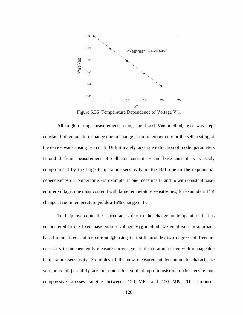
128
Figure 5.36 Temperature Dependence of Voltage VBE
Although during measurements using the fixed VBE method, VBE was kept
constant but temperature change due to change in room temperature or the self-heating of
the device was causing IC to drift. Unfortunately, accurate extraction of model parameters
IS and β from measurement of collector current IC and base current IB is easily
compromised by the large temperature sensitivity of the BJT due to the exponential
dependencies on temperature.For example, if one measures IC and IB with constant base-
emitter voltage, one must contend with large temperature sensitivities, for example a 1˚ K
change at room temperature yields a 15% change in IS.
To help overcome the inaccuracies due to the change in temperature that is
encountered in the fixed base-emitter voltage VBE method, we employed an approach
based upon fixed emitter current IEbiasing that still provides two degrees of freedom
necessary to independently measure current gain and saturation currentwith manageable
temperature sensitivity. Examples of the new measurement technique to characterize
variations of β and IS are presented for vertical npn transistors under tensile and
compressive stresses ranging between -120 MPa and 150 MPa. The proposed
T
0 5 10 15 20 25
V
BE
/VB
E
-0.05
-0.04
-0.03
-0.02
-0.01
0.00
VBE/VBE= -2.112E-03T

129
measurement technique forces a current from the emitter while keeping base and
collector terminals grounded as shown in Fig. 5.37. This measurement technique has only
two degrees of freedom (IB and VBE), so we can obtain and IS/IS data from this
measurement.
Figure 5.37 The Emitter Current IE Biasing of the
npn (Right) and pnp (Left) Transistor
Forcing current through the emitter causes IC to be nearly fixed, so the change in
IB determines the change in :
B
B
B
B
C
C
I
I0
I
I
I
I
(5.8)
Current gain is shown to be a quasi-temperaturecompensated quantity relative to
either the individual collector or base currents, with the residual temperature coefficient
limited by the bandgap difference between the base and emitter regions of the transistor
as discussed in the previous section.With this method, the base-emitter voltage is allowed
to change and by carefully recording the temperature data at each measurement point, the
temperature related change in VBE can be compensated. We can also correct for small IC
variations as changes by measuring, or calculating, IC/IC.
If there is no change in IC, we can obtain normalized change in IS using the
following equation:
IC
IB
C
B
E
IC
IB
C
B
E

130
T
T
V
V
kT
E6.1
V
V
I
I
T
BEGB
T
BE
S
S
(5.9)
Through careful measurement of temperature in a controlled oven, we can correct
for any temperature errors in Eq. (5.9) which effectively becomes:
T
BE
S
S
V
V
I
I
(5.10)
Figure 5.38 Change in Current Gain of an npn Transistor on (100)
Silicon using IE Sweep Method
By carefully monitoring any temperature change during measurements using a
thermistor we were able to correct for the variation in base emitter voltage VBE for any
error due to thermal drift. Examples of the emitter current biasing method to characterize
variations of saturation current IS and current gain under stress are presented in Figs.
5.38 and 5.39 for an npn transistor under tensile and compressive stresses ranging
between -120 MPa and 150 MPa. Figure 5.40 provides a comparison between a fixed
base emitter voltage VBE measurement and constant emitter current biasing. Both
methods yield almost identical results for of approximately -490 (1/TPa). Figure
5.41 shows the normalized change in saturation current IS for pnp transistors. The
Stress, (MPa)
-200 -100 0 100 200
Change in G
ain
,
-0.10
-0.05
0.00
0.05
0.10
npn # 2
Tension
Compression
S =- 482 (1/TPa)IC
IB
C
B
E

131
advantage of this method is we can obtain the variation of saturation current IS with
applied stress which were not possible with the previous methods.
Figure 5.39 Change in Saturation Current IS of an npn Transistor on (100)
Silicon using IE Sweep Method
Figure 5.40 Comparison Between Fixed VBE and Emitter
Current IE Biasing Method
Stress, (MPa)
-200 -100 0 100 200
Satu
ration C
urr
ent
Change, S
S
-0.10
-0.05
0.00
0.05
0.10
S/S = 6.94E-072
- 5.43E-04
Tension
Compression
IC
IB
C
B
E
npn # 2
IC
IB
C
B
E
IC
IB
C
B
E
VBE Fixed
(Max Gain)
VCE = 1 V
VB E Fixed
(Max Gain)
VC E =-1 V
Stress, (MPa)
-200 -100 0 100 200
Change in G
ain
,
-0.10
-0.05
0.00
0.05
0.10
Stress, (MPa)
-200 -100 0 100 200
Cha
ng
e in
Ga
in,
-0.10
-0.05
0.00
0.05
0.10
Tension
Compression
S =- 492 (1/TPa)
npn # 2
Tension
Compression
S =- 482 (1/TPa)
Fixed VBE Method IE Biasing Method
npn # 2

132
Figure 5.41 Change in Saturation Current IS of an pnp Transistor on
(100) Silicon using IE Sweep Method
5.5 Summary and Conclusions
In this chapter, we have characterized the response of bipolar junction transistors
(BJT) due to the application of mechanical stress. Test structures have been utilized to
characterize the stress sensitivity of vertical npn and pnp bipolar devices fabricated on
(100) and (111) silicon wafers. Uniaxial normal stresses were applied to silicon wafer
strips using a four-point-bending fixture to observe the stress-induced changes in the
electrical performance of the BJTs. The collector current and DC current gain were both
found to decrease with stress, while the base current was found to increase with stress for
npn transistors on (100) and (111) silicon. For pnp transistors the collector current and
base current were both found to decrease with stress, while the current gain was found to
increase with stress.The slope of the normalized current gain vs. stress response for both
Stress, (MPa)
-200 -100 0 100 200
Sa
tura
tio
n C
urr
en
t C
ha
ng
e, S
S
-0.10
-0.05
0.00
0.05
0.10
S/S = 8.59E-072 -2.72E-04
Tension
Compression
IC
IB
C
B
E
pnp # 1

133
npn and pnp transistors was found to be fairly constant for a variety of bipolar transistor
designs. For an npn transistor, the variation of current gain with stress demonstrates a
linear trend, but the corresponding collector current and base current shows nonlinearity
because of the presence of 2i
2i nn term present in the current expressions. For pnp
transistors the current gain variation shows a nonlinear trend, but one thing to be noticed
is that the response of a pnp transistor is very small compared to the npn transistor and
from a practical point of view, we can neglect the curvature terms in the plot.
Different methods of electrical measurements such as base emitter voltage VBE
sweep method, fixed VBEmethod, emitter current IE sweep method was discussed and the
corresponding advantages and the disadvantages of these methods were addressed. It has
been shown that accurate measurements can be done using non temperature-compensated
techniques with careful attention to the experimental measurements. We have developed
a new non-temperature compensated approach based upon fixed emitter current biasing
that still provides two degrees of freedom necessary to independently measure current
gain and saturation current, but with manageable temperature sensitivity.
All these experimentally obtained results using various measurement methods
guided us towards the development of theoretical formulations to accurately calculate the
electrical characteristics of these bipolar devices when subjected to fabrication and
packaging induced stress. This will help the circuit designers to include stress induced
changes in their designs hence helping them to correctly predict the response of the
bipolar devices in a circuit in a particular stress condition.

134
CHAPTER 6
THEORETICAL MODELING OF MECHANICAL STRESS EFFECT ON THE
PERFORMACE OF PRECISION ANALOG DEVICES
6.1 Introduction
It is well known that mechanical strains and stresses developed during the
fabrication, wafer level and BEOL processing, and subsequent packaging of precision
analog devices cause parametric shifts in their electrical performance. The stress/strain
destroys the crystal symmetry of the silicon lattice that causes shift in the energy bandgap
which results in changes in electron and hole carrier concentrations and their mobilities.
The changes in the carrier concentration and their mobilities are manifested through
modulation of currents or voltages at the terminals of these devices as discussed in the
previous chapter. In MOS devices, mobility variations primarily affect transistor
transconductance parameters which are related to the mobilities of the carriers whereas
bandgap changes affect threshold voltages. In bipolar junction transistors (BJTs), both
bandgap and the attendant minority carrier mobility variations affect various parameters
including saturation current, base-emitter voltage, and current gain. Additionally, long-
term strain/stress can lead to crystal lattice damage (defects and dislocations), creating
additional generation-recombination centers and leading to changes in minority carrier
lifetimes and interface charge that affect behavior of both MOS and bipolar transistors.
Stress affects the reliability and performance of stress sensitive circuits adversely.
Stress-induced device parametric shifts will affect the performance of analog circuits that

135
depend upon precise matching of bipolar and/or MOS devices, and can cause them to
operate out of specifications. Stresses can be induced by fabrication and assembly
processes such as shallow trench isolation, wafer backgrinding and dicing, TSV
formation, die attachment, and first level packaging (e.g. encapsulation). The resulting
stresses alter the relative characteristics of the transistors and the parametric shifts
ultimately reduce overall circuitmanufacturing yield and increase manufacturing cost.
The analog devices are usually more affected by stresses, therefore the circuits containing
these analog devices demonstrates more stress sensitivity. Circuits that are affected
include phase-locked loops (PLLs), digital analog converters (DACs), analog-digital
converters (ADCs), precision voltage references, op-amps, regulators, filters etc. which
have applications in electronics field such as cellular phones, wireless application
modules, PDAs, hand held devices and image capturing devices.MEMS transducer
structures and interface circuits can also be adversely influenced.
One thing to acknowledge is that the determination of stress sensitive circuits are
highly dependent on the technology used in the fabrication of these circuits and also the
end user requirement. As an example, in an application where high performance is
required, small modulation of the electrical output of the circuit is more likely to be a
serious design problem compared to a low performance requirement. That is why the
older generation circuits with larger device sizes and low performance, were not affected
as strongly by stress related issues. With the trend of device size scaling down by the
semiconductor industry, the stress related problems are more important since fabrication
and package induced stresses are problematic in small feature size devices. Moreover the

136
tendency of the industry towards high performance circuits make the circuits more
susceptible to stress.
In the previous chapter, endeavors have been made to characterize experimentally
the variations in current gain β, collector current IC, base current IB and saturation current
IS of npn and pnp bipolar transistors with the application of uniaxial stress. Using these
experimentally obtained data we attempt to develop a theoretical model that fits the
experimental data. In literature there are a few detailed investigations by Creemer et al.
to develop a theoretical model to characterize the stress effects on analog devices [154-
159]. Their proposed model was based on determining piezojunction coefficients by
fitting their theoretical model (similar to that for the piezoresistance effect) to the
experimentally obtained data. Although characterization of the piezojunction coefficients
that describe the variation of transistor saturation currents under stress has been explored,
there has not been a comprehensive modeling effort for use in circuit simulation. Here we
discuss a basic charge-control model for the transistor that adequately captures the
macroscopic impact of stresses on the BJT device characteristics and demonstrates its use
in exploring the behavior of analog circuits employing these devices. This leads to an
understanding of the dominant effects of stress on the basic BJT model parameters and
elucidates the roles of mobility and intrinsic carrier concentration.
The performance of a circuit in any mechanical stress environment should be well
known by a circuit designer so that during designing the circuit he/she can design the
circuits to minimize stress related variations. Therefore, the objective of this chapter is to
develop theoretical formulations for stress induced variations in the electrical
characteristics of the analog devices so that these formulations can be applied to

137
theoretically optimize transistor design, placement, orientation, and processing to
minimize the impact of fabrication and packaging induced die stresses.
6.2 Bipolar Junction Transistor Modeling
To develop a more fundamental understanding of the variation of the electrical
performance of bipolar transistors under mechanical stress, a theory has been developed
to model uniaxial stress-induced changes in the current gain of vertical bipolar junction
transistors on (100) and (111) silicon. The developed expressions are based on the
standard one-dimensional theory for a uniformly doped bipolar junction transistor as
shown in Fig. 6.1. For the bipolar transistor depicted in Fig. 6.1, the collector and base
currents, IC and IB, are related to the base-emitter and base-collector voltages VBE and
VCE in the forward-active region using a basic transport model,
B
C
A
CEBESBC
I
I and
V
V11
kT
qVexpIII
(6.1)
where βrepresents the current gain, VA is the Early voltage, k is the Boltzmann constant,
and T is absolute temperature.
Figure 6.1 Simplified Cross-Section of a Vertical npn Bipolar Transistor
pn
Collector
C B
n
Base
E
Active Base Region
Emitter
Emitter-Base
Junction Collector-Base
Junction IC IE IB
IC
IB
C
B
E
IC
IB
C
B
E
pn
Collector
C B
n
Base
E
Active Base Region
Emitter
Emitter-Base
Junction Collector-Base
Junction IC IE IB
pn
Collector
C B
n
Base
E
Active Base Region
Emitter
Emitter-Base
Junction Collector-Base
Junction IC IE IB
IC
IB
C
B
E
IC
IB
C
B
E
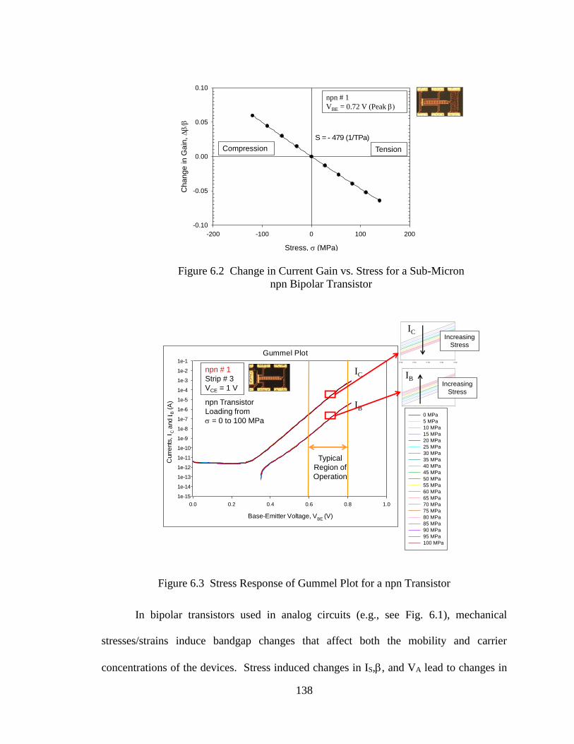
138
Figure 6.2 Change in Current Gain vs. Stress for a Sub-Micron
npn Bipolar Transistor
Figure 6.3 Stress Response of Gummel Plot for a npn Transistor
In bipolar transistors used in analog circuits (e.g., see Fig. 6.1), mechanical
stresses/strains induce bandgap changes that affect both the mobility and carrier
concentrations of the devices. Stress induced changes in IS,, and VA lead to changes in
Stress, (MPa)
-200 -100 0 100 200
Change in G
ain
,
-0.10
-0.05
0.00
0.05
0.10
TensionCompression
npn # 1
VBE = 0.72 V (Peak
S =- 479 (1/TPa)
Increasing
Stress
IB
0.718 0.719 0.720 0.721 0.722
Gummel Plot
Base-Emitter Voltage, VBE
(V)
0.0 0.2 0.4 0.6 0.8 1.0
Curr
ents
, C
and
B (
A)
1e-15
1e-14
1e-13
1e-12
1e-11
1e-10
1e-9
1e-8
1e-7
1e-6
1e-5
1e-4
1e-3
1e-2
1e-1
npn # 1
Strip # 3
VCE = 1 V
npn Transistor
Loading from
= 0 to 100 MPa
Typical
Region of
Operation
IB
IC
Increasing
Stress
IC
0 MPa
5 MPa
10 MPa
15 MPa
20 MPa
25 MPa
30 MPa
35 MPa
40 MPa
45 MPa
50 MPa
55 MPa
60 MPa
65 MPa
70 MPa
75 MPa
80 MPa
85 MPa
90 MPa
95 MPa
100 MPa

139
the I-V characteristics of the transistor (parametric shifts), and ultimately affect the
performance of analog circuits that depend upon precise matching of devices, causing
them to operate out of specifications. Fractional changes in collector current and current
gain based upon Eq. (6.1) at a given operating point are
B
B
C
C
A
A
CEA
CE
S
S
C
C
I
I
I
I and
V
V
VV
V
I
I
I
I
(6.2)
As examples, Figs. 6.2-6.5 illustrate data we have measured for variations of the
parameters of various vertical npn transistors subjected to moderate levels of uniaxial
stress. Fig.6.2 presents a typical change in npn current gain as a function of tensile stress
giving a 4.3% change for a 100 MPa tensile stress, corresponding to an effective
piezoresistive coefficient of -430/TPa. Fig.6.3 shows the changes in the Gummel plot for
the same BJT, and Fig. 6.4 presents further measurements of current gain versus tensile
stress over a wide range of bias conditions.
Figure 6.4 Current Gain vs. Base-Emitter Voltage and Stress for a npn Transistor
Base-Emitter Voltage, VBE
(V)
0.4 0.5 0.6 0.7 0.8 0.9
DC
Curr
ent g
ain
,
0
50
100
150
200
250 0 MPa
5 MPa
10 MPa
15 MPa
20 MPa
25 MPa
30 MPa
35 MPa
40 MPa
45 MPa
50 MPa
55 MPa
60 MPa
65 MPa
70 MPa
75 MPa
80 MPa
85 MPa
90 MPa
95 MPa
100 MPa
0.68 0.70 0.72 0.74 0.76 0.78
180
185
190
195
200
205
210
Increasing
Stress
npn # 1
Strip # 3
VCE = 1 V
Loading = 0 to 100 MPa
B
C
I
I

140
Fig.6.5 presents measured data for the stress dependence of Early Voltage. For the
case in which VCE is typically much less than VA as in low voltage submicron scale
devices, Eq. (6.2) indicates that we can neglect the impact of Early voltage changes on
collector current since VCE<< VA. Thus we focus here upon variations in ISand and
neglect changes in VA in the subsequent discussions.
Figure 6.5 Measured Early Voltage for an npn Transistor
Stress effects in p-n junction diodes and bipolar transistors, such as those depicted
above, have been reported by many investigators over the past 40 years [4, 136-146, 148,
150-159]. Such stress-induced phenomena in bipolar transistors have been collectively
referred to as the piezojunction effect in which the mechanical stresses/strains induce
bandgap changes that affect both the mobility and carrier concentrations of the device.
These effects cause variations in the saturation current SI of bipolar transistors:
2iS nI where µ represents the minority carrier mobility, and ni is the intrinsic carrier
concentration.
kT
EexpNNn wherenI G
VC2i
2iS (6.3)
Uniaxial Stress (MPa)
0 20 40 60 80 100 120
Early V
oltage,
VA
(V
)
0
20
40
60
80
100
120
IC = 50 A
Theil-Sen Estimator
y = -5.055E-02x+5.899E+01
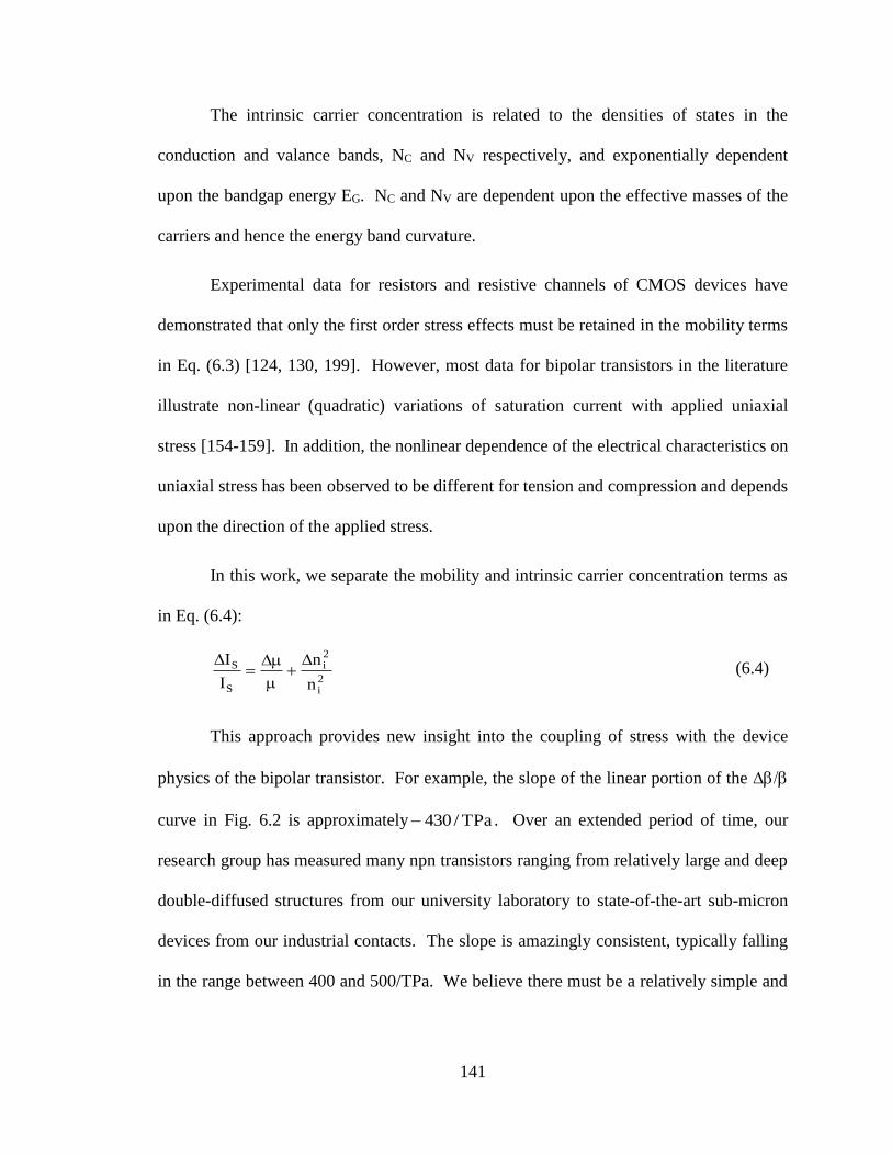
141
The intrinsic carrier concentration is related to the densities of states in the
conduction and valance bands, NC and NV respectively, and exponentially dependent
upon the bandgap energy EG. NC and NV are dependent upon the effective masses of the
carriers and hence the energy band curvature.
Experimental data for resistors and resistive channels of CMOS devices have
demonstrated that only the first order stress effects must be retained in the mobility terms
in Eq. (6.3) [124, 130, 199]. However, most data for bipolar transistors in the literature
illustrate non-linear (quadratic) variations of saturation current with applied uniaxial
stress [154-159]. In addition, the nonlinear dependence of the electrical characteristics on
uniaxial stress has been observed to be different for tension and compression and depends
upon the direction of the applied stress.
In this work, we separate the mobility and intrinsic carrier concentration terms as
in Eq. (6.4):
2i
2i
S
S
n
n
I
I
(6.4)
This approach provides new insight into the coupling of stress with the device
physics of the bipolar transistor. For example, the slope of the linear portion of the
curve in Fig. 6.2 is approximately TPa/430 . Over an extended period of time, our
research group has measured many npn transistors ranging from relatively large and deep
double-diffused structures from our university laboratory to state-of-the-art sub-micron
devices from our industrial contacts. The slope is amazingly consistent, typically falling
in the range between 400 and 500/TPa. We believe there must be a relatively simple and

142
fundamental explanation for this behavior. The theory developed in this chapter explains
these observations.
6.3 Piezoresistive Theory
Piezoresistance causes modulation of the electrical resistance of the material due
to the application of mechanical stress. In the past our group extensively investigated the
stress effects on resistors embedded on integrated chips. The relationship between resistor
sensor response and applied stress is fully developed [82, 84, 88] and explained in
Appendix A. The resistance of a conductor can be expressed in terms of resistivity ρ and
conductively σ as
punuq whereA
L1
A
LR pn
(6.5)
where L is the length of the resistor and A is its cross-sectional area. Piezoresistance is
caused by changes in the majority carrier mobility terms in Eq. (6.5) and the stress
dependencies are expressed differently on different silicon surfaces. Two surfaces of
primary interest here are depicted in Fig. 6.6. (100) silicon is now the most widely
utilized material for IC fabrication, whereas (111) silicon has been historically utilized
for bipolar transistor fabrication but is in more limited use today. In the following
sections, discussions on the basic piezoresistive formulations used on those surfaces are
presented.
6.3.1 (100) Silicon
The surface of the wafer is an (001) plane, and the [100] direction is normal to the
wafer surface. The primed coordinate system are along [110] and [110] directions which

143
are parallel and perpendicular to the primary flat of the wafer respectively. The
crystallographic axes for the wafer are along the unprimed axes whereas the primed
coordinate system is rotated 45˚ from the principal crystallographic axes. Eq. (6.6)
represents the standard theory for piezoresistive behavior of conductors in (100) silicon in
which the stresses in the resistance change equation are expressed as values in the
principal (crystallographic) coordinate system in Fig. 6(a) as presented in Appendix A
[77, 88].
2 2
11 11 12 22 22 11 22 12 11 33
2
11 33 12 11 22
2
44 12 13 23 1 2
Rl m
R
n
2 l m l n m n T T
(6.6)
(a) (b)
Figure 6.6 Principal and Primed Coordinate System for
(a) (100) silicon and (b) (111) Silicon
Note that the crystallographic axes are not in the plane of the (111) wafer.
Parameters π11, π12, and π44 are the three basic piezoresistive coefficients of
silicon, and l, m, and n are the direction cosines describing the orientation of the
conductor with respect to the [100] axis. The values of piezoresistive coefficients π11, π 12,
and π 44 are different for n- and p-type silicon.
x1 110[ ]
[100]
(100) Plane
x2 110[ ]
x2 010[ ]
x1 100[ ]
[111]
(111) Plane
]011[x1
]211[x2

144
6.3.2 (111) Silicon
The surface of the wafer is a (111) plane, and the [111] direction is normal to the
wafer plane. For (111) silicon, the crystallographic axes are not in the plane of the wafer,
so the changes in resistance are cast in terms of the primed coordinate system in Fig.
6.6(b). As mentioned previously, the resistance change of an arbitrarily oriented in-plane
resistor on the (111) surface can be expressed in terms of the stress components resolved in
this natural wafer coordinate system as described below:
2
1 11 2 22 3 33 2 3 23
2
2 11 1 22 3 33 2 3 23
2
2 3 13 1 2 12 1 2
1 11 12 44 2
RB B B 2 2 B B cos
R
B B B 2 2 B B sin
2 2 B B B B sin 2 T T ...
where
1 1 B ( ) B (
2 6
f
f
f
11 12 44 3 11 12 44
15 ) B ( 2 )
3
(6.6)
in which the “B” coefficients are convenient recurring combinations of the three basic
piezoresistive coefficients. In this case, the direction cosines are calculated relative to the
[110]axis.
6.4 Transistor Theory
We have found that the classic one-dimensional transistor model in Fig. 6.7 well
characterizes the basic behavior of a bipolar transistor and yields the desired insights into
the various stress dependencies. Fig. 6.7 includes the important currents in an npn device
including collector current IC and the two dominant components of base current: IBE
representing back injection into the emitter, and IBR representing recombination in the
base. As noted in Eq. (6.1), we are most interested in modeling collector current and

145
current gain, or equivalently collector current and base current, and to a lesser extent the
Early voltage.Note that the “horizontal” currents are all actually directed normal to the
wafer surface as in the transistor in Fig. 6.1.
The electrical conduction through the bipolar transistor is due to the minority
carriers. In case of a vertical npn transistor, electrons from the n-type emitter are injected
in the p-type base and diffuse to collector forming the collector current. Holes from base
get injected into the n-type emitter and form the base current. Some of the holes ended up
in combining with the electrons in the base forming the recombination current. Both
electrons and holes are minority carriers for both base and emitter respectively. The
diffusion current density is expressed by Eq. 6.8, where q is the charge, Dn and Dp are
the diffusion coefficient and dn/dx and dp/dx are the carrier gradients.
Figure 6.7 One Dimensional npn Transistor
+ -
+
+
-
-
-
-
-
+
+
+
+
+
+
VBE VBC
npn
E CB
+ ++ - -
nb0
nb
pe
pe0
IC
IBE IBR
WEWB
BRBEB
B
C
BR
BE
C
IIIgain with current I
I
ionrecombinat toduecurrent base I
emitter theinto
injectionback toduecurrent base I
currentcollector I
IBEIBR
Emitter Base
0
WEWB
ICpe
nb

146
dx
dpqDJ,Emittersiden
;dx
dnqDJ,Basesidep
pp
nn
(6.8)
For this diffusion process of electrons or holes to occur the diffusion current
density Jn or Jp should be constant which means the minority carrier concentration
gradient dn/dx or dp/dx must be constant or minority carrier distribution n or p must be
linear. Therefore in Fig. 6.7 the minority carrier distribution is shown as a linear
distribution, which is high at the injection point and gets low at the other boundary due to
diffusion.
6.4.1 npn Transistors on (100) Silicon
Using the classical bipolar transistor theory, the collector and base currents for the
npn transistor are expressed in the equations that follow in which GB and GE represent the
Gummel numbers in the base and emitter.
Collector Current
Base
A
Base
B2inB
B
BT
2inB
B
BC dx)x(Ndx)x(pG with n
G
qAVnD
G
qAI (6.9)
Base Current due to Back Injection
Emitter
D
Emitter
E2iEpE
E
TE2iE
E
pE
EBE dx)x(Ndx)x(nG and nG
VqAn
G
DqAI (6.10)
Base Current due to Recombination
nB
2iB
Base nB
0BBBR
nnnqAI
(6.11)
147
The normalized changes in the collector and base currents in Eq. (6.12) are found
from Eqs. (6.9- 6.11).
)T(fn
n
)T(fn
n
I
I
)T(f n
n
)T(fn
n
I
I
)T(fn
n
)T(fn
n
I
I
32iB
2iB
3
nB
nB
2iB
2iB
BR
BR
22iE
2iE
33pE112211
pE12
22iE
2iE
pE
pE
BE
BE
12iB
2iB
33nB112211
nB12
12iB
2iB
nB
nB
C
C
T
BE
T
BE
T
BE
T
BE
V
V
V
V
V
V
V
V+
(6.12)
The f1(T), f2(T) and f3(T) are the temperature terms associated with the
expressions of the transistor currents which will be discussed later in this chapter. The
coupling of stresses σ11 and σ22 on the chip surface into the vertical transistor currents are
characterized by π12, whereas the coupling of normal stress σ33 is characterized by π11.
The values of niE and niB may in fact differ due to bandgap narrowing in the emitter, and
it is possible that the fractional changes in intrinsic carrier concentrations in the base and
emitter under stress are not identical. This work actually indicates that they do appear to
be slightly different due to the effects of heavy doping. Thus the deformation potentials
may be different in the base and emitter.
6.4.2 pnp Transistors on (100) Silicon
The collector and base current expressions for the pnp transistors are similar to
those of the npn transistors with appropriate changes in the piezoresistive coefficients for
holes and electrons.

148
Collector Current
2BC T ipB
B
2pBC iB BE
52C pB TiB
2pB pB iB BE12 11 22 11 33 52
TiB
qAI V n
G
I n Vf (T)
I Vn
n Vf (T)
Vn
(6.13)
Base Current due to Back Injection
2E TBE iEnE
E
2
BE nE iE BE62
BE nE TiE
2nE nE iE BE12 11 22 11 33 62
TiE
qA VI n
G
I n V f (T)
I Vn
n Vf (T)
Vn
(6.14)
Base current due to recombination
2
B0 iBBR B
nB nBBase
2
BR iB nB72
BR nBiB
2
iB72
iB
p p nI qA
I n f (T)
I n
nf (T)
n
(6.15)
6.4.3 Current Gain
The overall current gains for both npn and pnp transistors can now be written as
II
I
BRBE
C
(6.16)
and

149
C CB BE BR
C B C BE BR
BE
BR BE
I II I I1
I I I I I
Iwhere 1
I I
(6.17)
Parameter δ represents the fraction of current gain that is determined by back
injection into the emitter. δ = 1 corresponds to 100% back injectionand δ = 0 corresponds
to 100% recombination.
The behavior of the base current IBwith collector-base voltage VBC changes can be
used to determine δ.Base current has two parts, back injection into the emitter IBE and
recombination current IBR. To understand the base current transport mode, the
experimental method applied was to modulate base width WB by increasing the reverse
collector-base voltage VCB while keeping either IBor VBEconstant as can be seen from Fig.
6.8. Therefore increase of the reverse bias increases the depletion region in the base
collector junction, that causes the base width to shrink, and as a result the minority carrier
concentration gradient changes slope. Since CI is proportional to minority carrier
concentration gradient, the shift in carrier concentration gradient causes collector current
to increase as can be seen from Eq. (6.8).This effect is known as the Early effect and is
characterized by Early voltage VA discussed earlier.
Figure 6.8 (Left) Demonstration of Early Effect in an 1D npn Transistor
(Right), The Biasing Used for Early Effect
Collector
IBEIBR
Emitter Base
0
WEWB
ICpe
ne
W ̒B
IC
IB
C
B
E
+
-VCE
+
-
VBE

150
At the same time, if the base width decreases there will be less recombination and if
the transistor is transport limited or the base current mainly comprises of recombination
current IBR then the change in base current IBwill be significant. Therefore, IBR should
show a dependence upon VCB since the recombination current is proportional to the total
minority carrier concentration in the base, whereas base current IBE, injected back into the
emitter, should be independent of VCB.
Figure 6.9 presents the normalized variations of npn and pnp currents and/or
voltages versus collector-base voltage. With constant IB in Fig. 6.9(a), the npn base-
emitter voltage dependence upon collector voltage is very small, yielding ≈ 1. For the
pnp transistor in Fig. 6.9(b), the results show approximately a 6:1 difference in the slopes
of the changes of the collector and base currents yielding 6/7. Therefore, in our
experiments the base current in the npn transistors on (100) silicon is mainly due to the
back injection of the holes and in case of pnp transistors it is due to the combination of
both back injection and some recombination, with the back injection current still
dominating.
Figure 6.9 Measured npn IC and VBE versus VCE(Left)
Measured pnp IC and IB versus VCE (Right)
Collector-Emitter Voltage (V)
-0.2 0.0 0.2 0.4 0.6 0.8 1.0 1.2 1.4
Norm
aliz
ed
Cha
ng
e
0.998
1.000
1.002
1.004
1.006
1.008
1.010
1.012
1.014
1.016
npn Collector Current
npn Base-Emitter Voltage
0.102x-1.229Ey
1.0 5x --4.01Ey
Collector-Emitter Voltage (V)
0.0 0.2 0.4 0.6 0.8 1.0 1.2 1.4 1.6
Norm
aliz
ed C
hange
0.98
0.99
1.00
1.01
1.02
1.03
1.04
1.05
pnp Base Current
pnp Collector Current
0.1x2E035.3y
0.1x3E267.5y

151
6.4.4 Overall npn and pnp Stress Dependencies
The stress dependencies resulting from the theory above for the npn and pnp
transistors on (100) silicon are consolidated in Table 6.1, and similar results appear in
Table 6.2 for transistors on the (111) surface in which the appropriate “B” coefficients
have been substituted in the expressions.
Table 6.1 Vertical Transistor Stress Dependencies for (100) Silicon
Parameter npn pnp
**
S
S
C
C
I
I and
I
I
)T(f
n
n
1
2iB
2iB
33nB112211
nB12
T
BE
V
V
2
pB pB iB12 11 22 11 33 2
iB
BE5
T
n
n
Vf (T)
V
BE
BE
I
I
)T(f
n
n
2
2iE
2iE
33pE112211
pE12
T
BE
V
V
2
nE nE iE12 11 22 11 33 2
iE
BE6
T
n
n
Vf (T)
V
BR
BR
I
I
)T(f
n
n32
iB
2iB
2
iB72
iB
nf (T)
n
nB pE nB pE
12 12 11 22 11 11 33
2 2
iB iE42 2
iB iE
n n f (T)
n n
pB nE pB nE
12 12 11 22 11 11 33
2 2
iB iE82 2
iB iE
n n f (T)
n n
Notes
removed. termTV/BEV with theCICI as same theisSISIfor expression The**
T
T
V
V
V
V
I
I
I
I
V
VexpII
II
I
I
I1
I
I
I
I
T T AA 0V
V
T
BE
T
BE
C
C
S
S
T
BESC
BRBE
BE
BR
BR
BE
BE
S
S
2.2p
4.2nBE
A
A
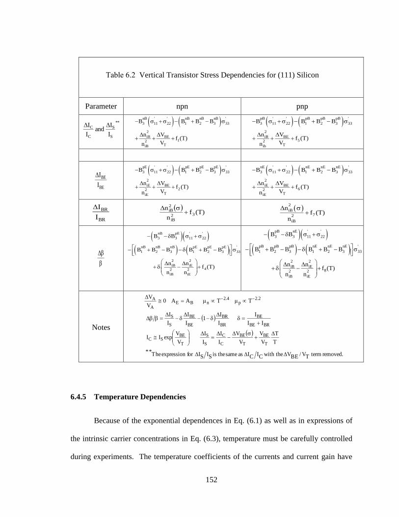
152
6.4.5 Temperature Dependencies
Because of the exponential dependences in Eq. (6.1) as well as in expressions of
the intrinsic carrier concentrations in Eq. (6.3), temperature must be carefully controlled
during experiments. The temperature coefficients of the currents and current gain have
Table 6.2 Vertical Transistor Stress Dependencies for (111) Silicon
Parameter npn pnp
**
S
S
C
C
I
I and
I
I
nB ' ' nB nB nB '
3 11 22 1 2 3 33
2
iB BE12
TiB
B B B B
n Vf (T)
Vn
pB ' ' pB pB pB '
3 11 22 1 2 3 33
2
iB BE52
Tib
B B B B
n Vf (T)
Vn
BE
BE
I
I
pE ' ' pE pE pE '
3 11 22 1 2 3 33
2
iE BE22
TiE
B B B B
n Vf (T)
Vn
nE ' ' nE nE nE '
3 11 22 1 2 3 33
2
iE BE62
TiE
B B B B
n Vf (T)
Vn
BR
BR
I
I
)T(f
n
n32
iB
2iB
2
iB72
iB
nf (T)
n
nB pE ' '
3 3 11 22
nB nB nB pE pE pE '
1 2 3 1 2 3 33
2 2
iB iE42 2
iB iE
B B
B B B B B B
n n f (T)
n n
pB nE ' '
3 3 11 22
pB pB pB nE nE nE '
1 2 3 1 2 3 33
2 2
iB iE82 2
iB iE
B B
B B B B B B
n n f (T)
n n
Notes
removed. termTV/BEV with theCICI as same theisSISIfor expression The**
T
T
V
V
V
V
I
I
I
I
V
VexpII
II
I
I
I1
I
I
I
I
T T AA 0V
V
T
BE
T
BE
C
C
S
S
T
BESC
BRBE
BE
BR
BR
BE
BE
S
S
2.2p
4.2nBE
A
A

153
been summarized in Table 6.3. Current gain has a much lower (30X) temperature
dependence than either the collector or base currents, and thus is much easier to
measure accurately.
6.4.6 Simplifications and Numerical Estimates
In order to understand and predict the expected transistor behavior from the
results in Tables 6.1 and 6.2, we need values for the piezoresistive coefficients for the
Table 6.3 Vertical Transistor Theory Temperature Dependencies
Paramete
r npn pnp
C
C
I
I
T
T18
T
T
V
V
kT
E6.1)T(f
T
BEGB1
GB BE5
T
E V Tf (T) 1.8
kT V T
BE
BE
I
I
T
T18
T
T
V
V
kT
E8.1)T(f
T
BEGE2
GE BE6
T
E V Tf (T) 1.6
kT V T
BR
BR
I
I
T
T19
T
T
V
V
kT
E3)T(f
T
BEGB3
GB BE7
T
E V Tf (T) 3
kT V T
GBE4
E Tf (T) 1.4 1.2
kT T
T0.6
T
GBE8
E Tf (T) 1.2 1.4
kT T
Notes
T
T
V
V
V
V
I
I
I
I
V
VexpII
II
I
I
I1
I
I
I
I
T T AA 0V
V
T
BE
T
BE
C
C
S
S
T
BESC
BRBE
BE
BR
BR
BE
BE
S
S
2.2p
4.2nBE
A
A

154
minority carriers and for the normalized changes in intrinsic carrier concentration versus
applied stress.
6.5 Intrinsic Carrier Concentration (ni)
At thermodynamic equilibrium, the product of the concentration of conduction
band electrons n and the concentration of the valence band holes p is equal to the square
of intrinsic carrier concentration (pn = ni2).. The intrinsic carrier concentration (ni) is a
constant for a semiconductor material. As can be seen from Eq. (6.3), nihas an
exponential dependence on bandgap and temperature of the material. The thermal
excitation will cause more electrons to get free from the valence band into the conduction
band causing the intrinsic carrier concentration to increase, the larger the bandgap, the
less thermally excited carriers will be able to get into conduction band from valence band.
The intrinsic carrier concentration is a function of densities of states in the conduction
and valance bands, NC and NV respectively. NC and NV are dependent upon the effective
masses of the carriers and hence the energy band curvature.
The intrinsic carrier concentration is significant in bipolar junction transistors
since electrical conduction in the BJTs happens due to the minority carriers, and the
intrinsic carrier concentration is used to determine the minority carrier concentrations as
can be seen from the from Eq. (6.18)
kT
BEqV
D
2i
ekT
BEqV
A
2i
b eN
npe
N
nn (6.18)
in which nb is electron concentration in the base and pe is the hole concentration in the
emitter. In Eq (6.18) NA is the doping in the p-type base and ND is the doping in n-type

155
emitter of an npn transistor. nband pe are both minority carriers in base and emitter
respectively.
Mechanical stress causes a shift in the conduction band and valence band edges of
the semiconductor and also in the density of states due to the redistribution of the carriers
which result in changes in intrinsic carrier concentration with stress. Creemer et al [154-
159] have calculated 2i
2i nn for uniaxial and shear stresses along different crystal
directions. They used kp̂ method based upon solid-state physics incorporating full
stress/strain relationship with deformation potentials from the theory of Bir and
Pikus[171]. Fig. 6.10 represents our quadratic fits to their data with the coefficients listed
in Table 6.4.
6.6 Minority Carrier Piezoresistive Coefficients
The expressions in Tables 6.1 and 6.2 involve piezoresistive coefficient data for
minority carrier mobilities, whereas the bulk of the available literature data piezoresistive
coefficient data is for majority carriers. This issue is addressed in Fig. 6.11 which
compares the majority and minority carrier mobilities from recent research results [200,
201]. As shown in the boxes in the Fig. 6.11, the emitter doping concentration is in the
range of the 1021/cm3 and the base doping is in the range of 10 17 to 10 18 /cm3. For typical
base and emitter doping levels, we observe that the pairs of majority and minority
electron and hole mobilities are very similar to each other. Since piezoresistive
coefficeints are proportional to mobilities of the carriers, so we assume here that the
piezoresistive properties of minority carriers are the same as those of majority carriers for
equivalent doping levels.

156
Figure 6.10 Calculations done by Creemer, et al. using kp̂ method
Employing Bir and Pikus Deformation Potential Theory
Table 6.4 Quadratic Fits to Theoretical Plots of Creemer [171]
Stress Orientation 2i
2i nn
[100] 426 10x755.210x644.1
[110] 427 10x403.310x873.8
[111] 427 10x387.310x285.5
Shear 2710x353.6
Stress (MPa)
-300 -200 -100 0 100 200 300
ni2/ni
2
-0.10
-0.05
0.00
0.05
0.10
0.15
0.20
Uniaxial (100)
Uniaxial (110)
Uniaxial (111)
Shear

157
Figure 6.11 Comparison of Majority and Minority Carrier Mobilities
versus Impurity Concentration
6.6.1 Piezoresistive Coefficient Simplifications
Table 6.6-A presents our best estimates of the complete set of piezoresistive
coefficients for use with npn and pnp bipolar junction transistors on (100) and (111)
silicon. These are based upon the original results of Smith [23], the work of Kanda[149],
and Cho[104].Table 6.6-B presents coefficient simplifications to help understand the
results and predict stress dependent behavior. First-order solid-state theory predicts
electrons to have a significant response to normal stress components and no response to
shear stress. In contrast, holes are predicted to have negligible response to normal
Carrier Mobilities: Majority and Minority Carriers
Lightly Doped Base
Heavily Doped Emitter

158
stresses and a large response to shear stresses. In addition, theory indicates that11 = -
212for electrons. The classical results of Smith [23]for lightly doped coefficients
support these theoretical results in which11 and 22are large for electrons, whereas44is
by far the largest coefficient for holes (Table 6.5). The other coefficients are much
smaller. It is also well known from the literature that the coefficients are significantly
reduced with moderate to heavy doping, and we can get estimates from the data of Cho
[104]regarding the magnitudes of the piezoresistive coefficients.
Table 6.5 Piezoresistive Coefficients in Lightly-Doped Silicon [41]
Coefficient n-type Si
(x 10-12 Pa-1)
p-type Si
(x 10-12 Pa-1)
11 -1020 +66
12 +534 -11
44 -136 +1380
S 11 12 -488 +55
1211D -1560 +77
B1 -311 +718
B2 +298 -228
B3 +61 -442
B1 - B2 -609 +946
3
2B
6
5B
2B 441211
3441211
2441211
1
The simplified coefficients in Table 6.6 result from application of the above
results for the basic dependence of holes and electrons due to stress:
1. Electrons have negligible response to shear stress. Thus 44≅ 0 in n-type silicon.
2. Holes only respond to shear stress. Thus 11and 12≅0 in p-type silicon.
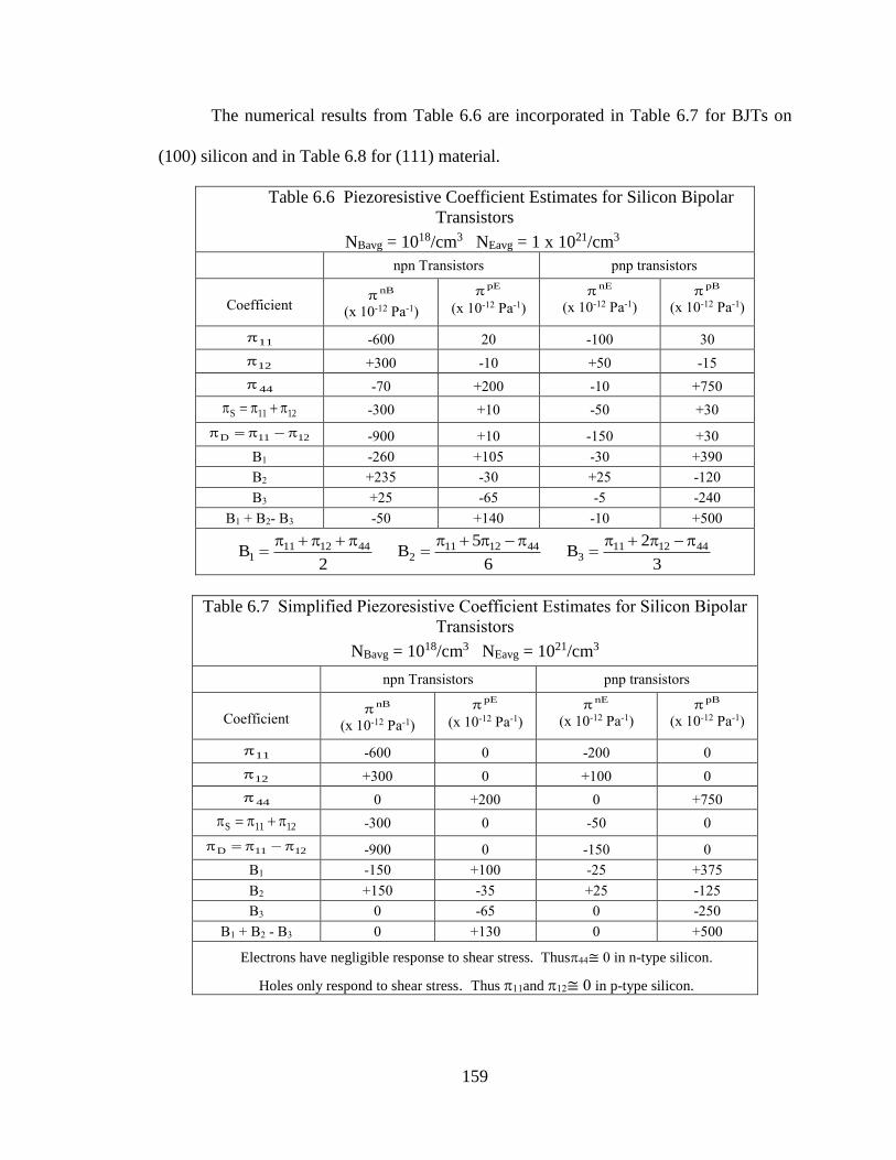
159
The numerical results from Table 6.6 are incorporated in Table 6.7 for BJTs on
(100) silicon and in Table 6.8 for (111) material.
Table 6.6 Piezoresistive Coefficient Estimates for Silicon Bipolar
Transistors
NBavg = 1018/cm3 NEavg = 1 x 10²¹/cm3
npn Transistors pnp transistors
Coefficient nB
(x 10-12 Pa-1)
pE
(x 10-12 Pa-1)
nE
(x 10-12 Pa-1)
pB
(x 10-12 Pa-1)
11 -600 20 -100 30
12 +300 -10 +50 -15
44 -70 +200 -10 +750
1211S -300 +10 -50 +30
1211D -900 +10 -150 +30
B1 -260 +105 -30 +390
B2 +235 -30 +25 -120
B3 +25 -65 -5 -240
B1 + B2- B3 -50 +140 -10 +500
3
2B
6
5B
2B 441211
3441211
2441211
1
Table 6.7 Simplified Piezoresistive Coefficient Estimates for Silicon Bipolar
Transistors
NBavg = 1018/cm3 NEavg = 1021/cm3
npn Transistors pnp transistors
Coefficient nB
(x 10-12 Pa-1)
pE
(x 10-12 Pa-1)
nE
(x 10-12 Pa-1)
pB
(x 10-12 Pa-1)
11 -600 0 -200 0
12 +300 0 +100 0
44 0 +200 0 +750
1211S -300 0 -50 0
1211D -900 0 -150 0
B1 -150 +100 -25 +375
B2 +150 -35 +25 -125
B3 0 -65 0 -250
B1 + B2 - B3 0 +130 0 +500
Electrons have negligible response to shear stress. Thus44≅ 0 in n-type silicon.
Holes only respond to shear stress. Thus 11and 12≅ 0 in p-type silicon.

160
6.6.2 Theoretical Model for Uniaxial Stress
It is much easier to understand what to expect based upon the simplified results in
Table 6.7. Equivalent arguments correspond to Table 6.8.
Table 6.8 Simplified Stress Dependencies – (100) silicon
Uniaxial Stress 11 22( ) .Vertical Transistors
Constant VBE – See Table 6.3 for Temperature Dependencies
Parameter npn Pnp
C
C
I
I
2iB
2iB
n
n
TPa
300
2iB
2iB
n
n
BE
BE
I
I
2iE
2iE
n
n
2iE
2iE
11n
n
TPa
100
BR
BR
I
I
2iB
2iB
n
n
2iB
2iB
n
n
2 2
iB iE
2 2
iB iE
n n300
TPa n n
2 2
iB iE
2 2
iB iE
n n100
TPa n n
Notes
76 pnp ; 1npn :storsour transifor of valuesMeasured
1II
I
I
I
I
I
I
I
BRBE
BE
BR
BR
BE
BE
C
C
6.6.2.1 pnp Transistors
Collector current variation in the pnp transistor is dominated by to variations
in intrinsic carrier concentration in the lightly doped base. Thus it provides a
direct test of the 2i
2i nn results of Creemer et al. [154-159].

161
pnp base current characterization is completed by adding a weak
pieozresistive term (100/ TPa) to the intrinsic carrier concentration variation.
Note that the expressions for niE and niB variations will both be present in the
total base current expression and may not be equal. Current gain would be
expected to have a linear response if the two intrinsic carrier concentration
terms were to cancel out. However our work shows that they do not cancel.
Table 6.9 Simplified Stress Dependencies – (111) Silicon
11 22( ) - Vertical Transistors - Silicon
Constant VBE – See Table 6.3 for Temperature Dependencies
Parameter npn pnp
C
C
I
I
2iB
2iB
n
n
2iB
2iB'
11n
n
TPa
250
BE
BE
I
I
2iE
2iE
n
n
TPa
65
2iE
2iE
n
n
BR
BR
I
I 2
iB
2iB
n
n
2iB
2iB
n
n
2 2
iB iE
2 2
iB iE
n n65
TPa n n
2 2
iB iE
2 2
iB iE
n n250
TPa n n
Notes 1
II
I
I
I
I
I
I
I
BRBE
BR
BR
BR
BE
BE
C
C
6.6.2.2 npn Transistors
Collector current variation in the npn transistor is similar to base current in the
pnp, with a substantial linear mobility term added to variations in intrinsic
carrier concentration in the lightly doped base.

162
npn base current is almost entirely due to back injection into the emitter and
provides direct look at intrinsic carrier concentration variations in the heavily
doped emitter.
Current gain would be expected to have a linear response from mobility
variations if the two intrinsic carrier concentration terms cancel out. Again,
our work indicates they often do not cancel. See discussion concerning Fig.
6.12 in next section.
Similar simplification results appear in Table 6.8 for (111) silicon.
6.7 Correlation of Theory with Experimental Results
6.7.1 (100) Silicon
Our test transistors come from a complementary bipolar technology with npn and
pnp transistor test devices in close proximity to each other, so we expect the intrinsic
carrier changes in emitter and base to be similar both both npn and pnp transistor.
Therefore, our work provides a unique chance to explore the differences between the
stress behavior of the intrinsic carrier concentrations in the base and emitter.
pnp Transistors:
According to Table 6.7, the collector current of the pnp transistor will directly
mirror the changes of intrinsic carrier concentration in the base. In Fig. 6.12, the
comparison between the theory and the experimental data of the pnp collector current is
presented. The solid line represent fits of the numerical results in Fig. 6.10 and Table 6.6
to the data. As evident from the plot, the pnp collector current data is almost an exact fit
to numerical values in Table 6.4 verifying the calculations of Creemer et al. [170-175].

163
Figure 6.12 Comparison of pnp Collector Current with Theory
As mentioned earlier in this chapter that base current in pnp transistor has
combination of both the back injection current and the recombination current and
indicated a δ ≈ 6/7. The base current expression for pnp transistor is shown in Eq. 6.19.
2 2 2
B nEpnp iB iE iB12 2 2 2
Bpnp iB iE iB
I n n n
I n n n
(6.19)
Fig. 6.13 shows the correlation between the pnp base current experimental data
and that of theory. The theoretical fit shown in the plot is achieved with a 100/TPa
piezoresistive coefficient and assuming intrinsic carrier concentration change in both
emitter and base to be equal. The base current fit with theory shows a good correlation
with some discrepancies at the extremities. This discrepancies can be due to the fact that
the intrinsic carrier changes with stress in base and emitter are not same. This is because
there may be some bandgap narrowing due to the heavy doping in the emitter.
Uniaxial Stress [110] (MPa)
-200 -100 0 100 200
Norm
aliz
ed C
hange o
f pnp C
olle
cto
r C
urr
ent C
/C
-0.06
-0.04
-0.02
0.00
0.02
0.04
0.06
0.08
pnp Collector Current Expt. Data
Intrinsic Carrier Conc.

164
Figure 6.13 Comparison of pnp Base Current with Theory
Figure 6.14 Comparison of pnp Current Gain with Theory
In Fig. 6.14 the comparison between the theoretical and experimental results of
the pnp current gain is presented. The plot shows that the experimental current gain plot
Uniaxial Stress [110] MPa
-200 -100 0 100 200
Norm
aliz
ed C
hange o
f pnp C
olle
cto
r C
urr
ent
/
-0.08
-0.06
-0.04
-0.02
0.00
0.02
0.04
0.06
0.08
0.10
pnp Base Current Expt. Data
pnp Base Current from Theory
Uniaxial Stress [110] MPa
-200 -100 0 100 200
No
rmaliz
ed C
han
ge
in
Cu
rre
nt
Ga
in
-0.08
-0.06
-0.04
-0.02
0.00
0.02
0.04
0.06
0.08
pnp Current Gain Expt. Data
pnp Current gain from Theory

165
is almost a pure quadratic plot. The theoretical fit is again without considering the
changes in intrinsic carrier concentration due to bandgap narrowing. If both the intrinsic
carrier changes were same the plot would have showed a linear trend as can be seen from
the theoretical fit. As mentioned earlier the reason for this divergence may be due to the
bandgap narrowing under stress.
npn Transistors:
In case of npn, measurements results of δ in Fig. 6.9(a) indicate that the base
current of the npn is all due to back injection into the emitter so that the npn base current
will provide a view of the changes of intrinsic carrier concentration in the emitter, but
may exhibit differences due to heavy doping effects in the emitter.
Figure 6.15 Comparison of npn Currents with Theory
Fig. 6.15 compares our experimental data with theoretical results for npn collector
and base current. The solid line in Fig. 6.15 corresponds to the combination of the
theoretical results in Fig. 6.10 and Table 6.6, and the data points are the experimentally
Stress, MPa)
-200 -100 0 100 200
Curr
ent C
ha
ng
e,
-0.10
-0.05
0.00
0.05
0.10
C - Experiment
- Experiment
C - Theory
- Theory

166
obtained values. As the theory predicts, the npn transistor base current should match with
the changes of intrinsic carrier concentration as in Fig. 6.10, and adding a linear
piezoresistive term to the base current change should give the change in collector current.
But Fig. 6.15 shows that the experimental data and the theoretical predictions are not
quite matching. However for the base current of the npn, the same numerical results of
the change in intrinsic carrier concentration with stress provide an excellent fit to the data,
when the curve is shifted to account for a built-in stress in the emitter of 150 MPa. The
procedure to obtain the built-in stress is discussed in the following,
The change in intrinsic carrier concentration from Creemer can be expressed as:
22B iE
2B Theory iE
I nA B
I n
(6.20)
This change in intrinsic carrier concentration in Eq. (6.20) should match with the
change in base current in npn transistor in absence of any built-in stress in the emitter.
However, presence on any built-n stress will cause the change in intrinsic carrier
concentration in Eq. (6.20) to shift by
2 2BS S
B Theory
IA( ) B( )
I
(6.21)
where σS is the built-in stress. Now to find out the required shift of the theoretical plot to
match with the experimental data, least square method was applied. The required shift
minimizes the least square error between the data points and theory as shown in Eq. 6.22.
2
n2 2 B
i S i S
i 1 B i
IA( ) B( )
I
(6.22)

167
Minimizing Eq. (6.22) yields the value of the required shift σS of the theoretical intrinsic
carrier change that needs to be incorporated to match with the experimental data.
Figure 6.16 Comparison of npn Currents with Theory
A Matlab code was written to find out the required shift in the theoretical plot to
match the experimental data provides the built-in stress to be 150 MPa. The correlation of
the theory and experimental results with the built-in stress is presented in Fig. 6.16. The
red solid line is the theoretical change in intrinsic carrier concentration with the built-in
stress shift, whereas the blue line utilizes the same data as the pnp collector current along
with an added piezoresistive term of 200/TPa. Both collector current and base current
experimental data show excellent agreement with the theoretically obtained plots. The fit
of the curve is highly sensitive to the value of the shift, and we believe this measurements
represent an excellent method for quantifying built-in stress due to a combination of
heavy doping effects and fabrication processes such as in the shallow trench isolation,
polysilicon emitter processes, etc.
Stress, (MPa)
-200 -100 0 100 200
Curr
ent C
ha
ng
e,
-0.10
-0.05
0.00
0.05
0.10
C/ C
B/ B
.vsI
I
B
B
.vsI
I
C
C
Built in Stress = +150 MPa

168
Figure 6.17 Comparison of npn Current Gain with Theory
Fig. 6.17 compares theory and experiment for the current gain of the npn
transistor. The experimentally obtained current gain variation is quite linear with a small
curvature. For theoretical evaluation of the current gain, the base current variation is
subtracted from the collector current variations obtained from theoretical fits. This
subtraction yields a strictly linear curve since both the collector current and base current
variation is quadratic in nature. The yielding of a linear plot from the subtraction of the
quadratic plots can be explained as shown in the following. The simplified numerical
expressions for base current variation with the built-in stress and collector current can be
expressed as
22C iB
2 12C iB
22B iE
2 S 1 S2B iE
2 22C B iB iE
2 S 2 S 1 S2 2C B iB iE
I nC C
I n
I nC C
I n
I I n n2C C C
I I n n
(6.23)
Uniaxial Stress [110] (MPa)
-200 -100 0 100 200
Norm
aliz
ed C
hange
in
Cu
rre
nt G
ain
-0.10
-0.05
0.00
0.05
0.10Current Gain Expt. Data
Current Gain from Theory

169
where σS is the built-in stress. Therefore from Eq. 6.23, it is evident that subtracting two
equal quadratic terms will yield a straight line. As a result the variation of npn current
gain is found out to show a linear trend. Any curvature in the current gain plot
corresponds to a slight difference in the quadratics due to heavy doping.
6.6.3 (111) Silicon
We have limited access to devices on the (111) surface. However, we have been
able to operate one of our van der Pauw structures as a vertical npn transistor.
Figure 6.18 (111) Transistors Under Uniaxial Stress: npn Normal-Mode
Current Gain. Straight Line Represents Least Square Fit to the Data.
The current gain fits the theory for the npn device on (111) silicon. The structure
utilized has similar sheet resistances for the base and emitter diffusions and hence the
intrinsic carrier concentration terms should cancel out leaving only the mobility term
equal to the slope in Fig. 6.18 (-53/TPa). has not been determined for this device but is
expected to be ˂ 1.
Uniaxial Stress [110] (MPa)
0 20 40 60 80 100 120
Norm
aliz
ed C
hange in C
urr
ent G
ain
/
-0.006
-0.005
-0.004
-0.003
-0.002
-0.001
0.000
y = -5.25E-05x

170
(111) npn current gain theory:
2 2
iB iE
2 2
iB iE
n n65
TPa n n
(6.25)
6.6.4 Systematic Approach to Parameter Extraction
The list below represents an extraction process that can be used to fit the theory to
the data.
npn
1. Use validated theoretical result for 2iB
2iB
n
n
2. Determine value of nB
12 needed to fit collector current data.
3. Determine “built-in” stress necessary to fit
and hence
B
B
I
I
pnp
1. Use validated theoretical result for 2iB
2iB
n
n
2. Determine value of pB
12 and “built-in” stress needed to fit current gain and base
current data.
6.7 Conclusions
We have demonstrated that classic one-dimensional bipolar junction transistor
adequately models the stress dependent behavior of BJTs and provided a systematic
approach to extraction of the necessary stress dependent parameters in the model for npn
and pnp transistors. Collector current and base current variations are dominated by

171
intrinsic carrier concentration variations, whereas current gain tends to be nearly linear
with a small quadratic term. It has been shown that Early voltage variations can be
neglected.
Theoretical results for variations of intrinsic carrier concentration under stress
provide excellent fits to data related to base transport, whereas those for heavily doped
emitters require the assumption of a built-in stress. In fact, measurements versus applied
uniaxial stress appear to provide a highly sensitive means of measuring the built-in stress
in the emitter since the moderately doped base regions show no indication of built-in
stress. Stress measurements also indicate an apparent change in the deformation
potentials in heavily doped silicon.

172
CHAPTER 7
MECHANICAL STRESS EFFECTS ON BIPOLAR ANALOG CIRCUITS
7.1 Introduction
In this chapter, the impact of mechanical stress on several bipolar basic analog IC
building blocks is demonstrated and discussed. In previous chapters, the focus was on
how the device parameters of bipolar transistors change due to mechanical stress and the
development of theoretical formulation by incorporating the stress induced changes in
device characteristics based on the experimentally obtained data. The understanding of
the stress induced device parameter modulations of individual npn and pnp transistors can
be utilized to predict the changes in the circuit output containing these transistors.
This chapter deals with the experimental investigation of the impact of stress on
few basic bipolar analog circuits such as PTAT (Proportional-to-Absolute-Temperature)
voltage generators, offset voltage of differential pairs and current mirrors. Stress response
of these circuits are presented in this chapter and furthermore correlation of the stress
dependent transistor models with the measurements of these circuits are established.
7.2 Stress Induced Changes in Circuit Output
The basic building block of bipolar ICs usually consist of resistors, standard npn
and pnp transistors, substrate pnp’s and diodes (diode connected transistors). The
performance of the circuits is affected due to the stress induced parametric shifts of the

173
circuit elements due to the piezo effects experienced by these elements.
In this section, experimental study of the changes in some basic bipolar analog
circuit outputs are reported due to application of mechanical stress. These basic circuits
were constructed by connecting adjacent npn or pnp transistors situated on the (100)
silicon wafer strips as shown in Fig. 7.1. A total of 15 different npn and pnp transistors
with various transistor area sizes were present in the (100) wafer strip. Uniaxial normal
stress was then applied along the ]101[ direction to the silicon strips cut from the
processed wafers containing the bipolar circuits using a four point bending loading
fixture as shown in Fig. 7.2. The same method was used to apply the uniaxial stress on
the circuits as that was used for individual npn and pnp transistors on wafer strips as
explained in Chapter 5. In the following subsections the stress induced changes PTAT
voltage generators, differential pair offset voltages and the mirror ratio of current mirrors
are explored and discussed.
Figure 7.1 Bipolar Transistor Wafer Strip on (100) Silicon
Vertical BJT Test Structures
BJT Stress Cell
(15 Different BJT Designs)
(100) Silicon

174
Figure 7.2 Application of Uniaxial Stress to Bipolar Circuits
7.2.1 Stress Response of the Offset Voltage of Differential Pairs
One of the most common and important circuits in bipolar ICs is an npn or pnp
differential pair. Fig. 7.3 shows a simple npn differential pair. Q1 and Q2 are two npn
transistors with the best matching of VBE where the collectors of both the devices are
connected together so that the collector-emitter voltages are equal. The base of Q1 is
connected to a voltage supply whereas the base of the Q2 is grounded. The emitters of
Q1and Q2 share a commonconnection through which current is pulled out of the circuit as
shown in Fig. 7.3.
Figure 7.3 npn Differential Pair
Applied Stress
Direction
Transistor
Structure
Wafer Strip
]110[x
]101[y
Applied Stress
Direction
Transistor
Structure
Wafer Strip
]110[x
]101[y
In-Plane
Uniaxial Stress
In-Plane
Uniaxial Stress
V1
50µA
Q1Q2
npn 1npn 2
IC1 IC2
VBE1 VBE2
+
-
+
-
IE

175
Considering the npn differential pair,also referred to as emitter-coupled pair, as
shown in Fig. 7.3, from Kirchhoff's voltage law for the input loop, it can be written:
1 BE1 BE2V V V 0 (7.1)
For the bipolar transistor, the collector current ICis related to the base-emitter voltage VBE
in forward bias region as shown in Eq. (7.2).
BEC S
T
VI I exp
V
(7.2)
where IS saturation current and VT is the thermal voltage. Therefore for both npn
transistors it can be written as,
BE1C1 S1
T
VI I exp
V
(7.3)
and
BE2C2 S2
T
VI I exp
V
(7.4)
Offset voltage is defined as the voltage required to set IC2= IC1 in the circuit in Fig
7.3. Setting IC1 = IC2 yields:
S1 BE2 BE1
S2 T
S1O S T
S2
I V Vexp
I V
which becomes
IV V ln
I
(7.5)
where VOS = VBE1-VBE2, which is the offset voltage between two transistors.
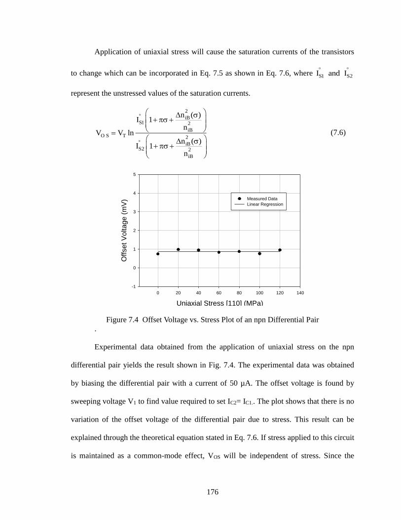
176
Application of uniaxial stress will cause the saturation currents of the transistors
to change which can be incorporated in Eq. 7.5 as shown in Eq. 7.6, where S1 S2I and I
represent the unstressed values of the saturation currents.
2
iBS1 2
iBO S T 2
iBS2 2
iB
n ( )I 1
nV V ln
n ( )I 1
n
(7.6)
Figure 7.4 Offset Voltage vs. Stress Plot of an npn Differential Pair
.
Experimental data obtained from the application of uniaxial stress on the npn
differential pair yields the result shown in Fig. 7.4. The experimental data was obtained
by biasing the differential pair with a current of 50 µA. The offset voltage is found by
sweeping voltage V1 to find value required to set IC2= IC1.. The plot shows that there is no
variation of the offset voltage of the differential pair due to stress. This result can be
explained through the theoretical equation stated in Eq. 7.6. If stress applied to this circuit
is maintained as a common-mode effect, VOS will be independent of stress. Since the
Offset Voltage vs. Stress
Uniaxial Stress [110] (MPa)
0 20 40 60 80 100 120 140
Off
se
t V
olta
ge (
mV
)
-1
0
1
2
3
4
5
Measured Data
Linear Regression

177
stress was applied along ]101[ direction and current flow through both the transistors in
the circuit are perpendicular to the direction of stress, the saturation currents in both the
transistor should be affected by stress in similar way, hence no significant change in the
offset voltage of the circuit should occur.
7.2.2 Stress Response of PTAT Circuit
In this section, the uniaxial stress effect on a PTAT circuit is discussed. Fig. 7.4
shows a typical configuration of a PTAT circuit. The two transistors in a PTAT circuits are
operated at different current densities, which effectively produces a voltage difference
between two transistors (an offset voltage). The difference in voltage is proportional to
absolute temperature (PTAT) and depends on the emitter area ratio and the collector
currents of the devices
Figure 7.5 PTAT Circuit
The expression for PTAT voltage can be written following the same procedure
explained in previous section. Similar expression can be written for PTAT circuit as in
Eq. 7.5 for perfectly matched npn transistors,
C2 S1PTAT BE1 BE1 T
C1 S2
I IV V V V ln
I I (7.7)
50µA
Q1Q2
npn 1 npn 2
IC1 IC2
VBE1 VBE2
+
-
+
-
10µA

178
Introduction of stress induced changes in Eq. 7.7, we can write
2
iBS1 2
iBC2PTAT T 2
C1 iBS2 2
iB
n ( )I 1
nIV V ln
I n ( )I 1
n
(7.8)
Since the stress state is the same in both transistors, the change in saturation current for
the transistors should be same, as in the npn differential pair. Therefore for
1 2 S1 S2 1 2 PTAT TFor I 5I with I I and ,V V ln(5) 0.0259V 1.609 41.7 mV
.Th
e theoretical evaluation shows that the PTAT output voltage should not change with
stress and if the collector current ratio between both the transistors is 1:5 then VPTAT
should be 41.7 mV.
Figure 7.6 PTAT Output Voltage vs. Uniaxial Stress
To obtain a correlation between theory and experiments, we have performed
experimental measurements on a PTAT circuit as shown in Fig. 7.4 by applying uniaxial
stress. Transistor Q1 was supplied with a collector current of 10 µA current whereas Q2
was supplied with a current of 50 µA. The resultant plot is shown in Fig. 7.5. The
PTAT Cell Output Voltage
Uniaxial Stress [110] (MPa)
0 20 40 60 80 100 120
PT
AT
Cell
Outp
ut V
oltage (
mV
)
36
38
40
42
44
Measured Data

179
experimental data shows that PTAT output voltage is around 41.5 mV and that the PTAT
voltage does not change with stress which agrees with what theory has predicted.
7.2.3 Stress Response of Current Mirror
The current mirror is another important building block of bipolar integrated
circuits that we have investigated in this chapter. A current mirror is a current source that
provides fixed bias current and/or active loads to other analog circuits. The devices in the
ideal current mirror should be identical so the output current of the circuit (IO) replicates
the collector current (IC1) of Q1.
Figure 7.7 Current Mirror Circuit
The basic bipolar current mirror\ shown in Fig. 7.5 consists of two npn identical
transistors Q1 and Q2 whose bases are connected and the base and collector of Q1
transistor is joined to provide a negative feedback. If the two transistors Q1 and Q2are
properly matched, then mirror circuit output current IO will be same as the collector
current of Q1.
IC(1+1/β)
Q2Q1npn 2npn 1
ICIO=IC
IREF
IC/β
IC(1+1/β)
IC/β
2IC/β
V0

180
Applying Kirchhoff's current law at node Q1,
REF C B C
2I I 2I I 1
(7.9)
where β is the current gain of the transistors in which both Q1 and Q2 are matched
perfectly. If the emitter area of both the transistors are not same, i.e.; S1 S2I mI then Eq.
7.9 can be written as:
REF C
(m 1)1
I Im
(7.10)
In a current mirror, the output current follows the collector current of Q1
transistor, i.e.; IC = IO, hence,
O
REF
I m
I (m 1)1
(7.11)
Due to mechanical stress, there will be changes in the output current of the current
mirror circuit due to the changes in current gain of the device as evident from Eq. 7.11.
Incorporating the stress induced changes in the current gain in Eq. 7.11, the change in
output current of the current mirror circuit due to stress can be written as,
O
O 0 0
I
I (m 1)
(7.12)
where β0 is the stress free current gain. Substituting 2 2
iB iE
2 2
iB iE
n ( ) n ( )
n n
, m
= 3 and using appropriate values for the piezoresistance coefficient π and the intrinsic
carrier concentration, ni in Eq. 7.12, Fig 7.6 can be obtained. From the plot it is evident
that for a 30 µA of output current in stress free case, an application of 100 MPa stress will

181
cause the output current of the circuit to change approximately 23 nA. This change in
output current will affect the performance of the current mirror circuit that is usually used
in analog IC to provide a fixed bias current or load to other circuits. Note that changes in
the saturation currents cancel out just as in the previous two circuits, as long as the stress
is the same in both transistors.
Figure 7.8 Output Current Change Vs. Stress of Current Mirror Circuit (Theory)
Figure 7.9 Output Current Change vs. Stress of Current Mirror Circuit (Experiment)
Uniaxial Stress [110] (MPa)
0 20 40 60 80 100 120 140
Change in O
utp
ut C
urr
ent,
-0.0010
-0.0008
-0.0006
-0.0004
-0.0002
0.0000
Output Current Change from Theory
O
O
I7.711E 06
I
Uniaxial Stress [110] (MPa)
0 20 40 60 80 100 120 140
Change in O
utp
ut
Curr
ent,
-0.0012
-0.0010
-0.0008
-0.0006
-0.0004
-0.0002
0.0000
Output Current Change from Experiment
O
O
I8.362E 06
I

182
For experimental investigation of the uniaxial stress effect on an npn current
mirror circuit, the circuit configuration shown in Fig. 7.5 was assembled in a wafer strip
and an uniaxial stress of 0 to 120 MPa was applied. The emitter area ratio m between two
npn transistors in the circuit was 3 and the input current IREF was set to 10 µA, which
resulted in an output current of approximately 30 µA. The plot of the experimentally
obtained data is shown in Fig. 7.7. The theoretically result in Fig. 7.8 shows excellent
agreement with the experimentally obtained data presented in Fig. 7.9.
7.3 Conclusion
In this chapter, the impact of uniaxial stress on several basic analog circuits are
investigated. The stress dependent transistor models are correlated with the
experimentally obtained stress response of the circuits to demonstrate the impact of stress
on basic analog IC building blocks.Measurements agree well with the theoretical model
for PTAT voltage generators, the offset voltage of differential pairs and the mirror ratio
of current mirrors. Therefore, the theoretical model can be effectively implemented to
obtain the impact of stress on bipolar analog circuits.

183
CHAPTER 8
CONCLUSIONS
In this thesis, the effect of mechanical stresses in several electronic devices have
been explored and discussed. The stress sensor aspect of some devices such as resistors
and field effect transistors, are discussed and research related to that topic is addressed.
For bipolar junction transistor the stress induced changes in the electrical characteristics
are characterized experimentally and a related theoretical work has also been discussed in
this thesis to address the stress related shifts in bipolar transistors.
In Chapter 1, an overview of the sources of mechanical stress generation due to
the fabrication, processing and packaging of the integrated circuit chips are discussed in
detail. The thermal expansion coefficient mismatch and the mechanical property
mismatch between the materials used in IC processing are the causes of stress generation.
Stress can also be generated due to the intrinsic stress on the deposited film, thermal
oxidation of silicon and, lattice mismatch between different implanting material in silicon
etc. The scaling down of the devices and increase in circuit density are causing more
complicated stress patterns in IC chips. The impact of stress on silicon chip is also
presented in Chapter 1.
The stresses and strain in the integrated circuit chips cause parametric shifts in the
electrical performance of the electrical devices in the circuit and affects their output
184
performance. The reason behind these parametric shifts are attributed to the
piezoressistance and piezojunction effects of semiconductor devices. Silicon being a
cubic crystal, the stress and strain causes the crystal symmetry of the silicon to alter and
that causes the electrical characteristics such as the resistivity or the saturation current of
the devices to change. The piezoresistance effect causes alterations of the resistivity of
the resistors and field effect transistors and this effect is due to the changes in majority
carrier mobility. This effect is extensively studied by various researchers and the physics
behind the changes in mobility of the carriers due to the changes in the band structure of
the silicon is very well understood. The piezojunction effect is attributed to the variations
in saturation current of p-n junctions and bipolar transistors and the variation in minority
carrier mobility and the changes in the intrinsic carrier concentration causes this effect
since this devices operate due to the conduction of minority carriers. There are few
researchers who studied this effect in details. The literature review on piezoresistive
effect and piezojunction effect is discussed in Chapter 2.
Chapter 3 focuses on the piezoresistive effect of multi element resistor stress
sensor rosettes capable of measuring die stresses in packaged electronic modules. The
piezoresistive theory for resistor sensors are fully developed and a review of that theory is
presented in Appendix A. The piezoresistive theory for various rosette design in various
silicon wafer surface is also discussed in Chapter 3. To extract stress distribution on a
silicon die, the change in resistance values of the resistor elements, piezoresistance
coefficients and the change in temperatures are needed to be known. For stress
characterization, the parameters required are obtained from experimental data. There can
be uncertainties in acquiring these parameters due to the errors made during the
185
experiments and due to these uncertainties in measured values there can be significant
errors in the extracted stress values. To determine the effect of these uncertainties in the
extracted stress values, a sensitivity of the stresses to these parameters are explored. For
that reason, the stress distribution over the die of a flip chip package is obtained from
finite element analysis and using those stresses the sensitivity analysis is performed. The
results show that the sensitivities are stress dependent and that temperature compensated
measurements should be performed because they are associated with low sensitivities.
Chapter 4 deals with the piezoresitive effect on field effect transistors (FETs) and
the operation of this device as a potential stress sensor. The smaller geometrical size of
the device and also its lighter doing of the resistive channel makes it advantageous over
the resistor sensors. In this chapter the dependence of the piezoresistive coefficients on
the operating point of the device is discussed. The calibration of the piezoresistance
coefficients are performed by applying uniaxial stress. The piezoresistance coefficients
are expressed as a function of drain current to demonstrate its dependence to operating
point. Piezoresistance coefficients corresponding to the PMOS devices exhibit linear
dependence on the drain current whereas for NMOS devices shows a nonlinear trend.
The piezoresistance coefficients are also expressed as a function of carrier mobility in the
channel region. At low currents high sensitivity can be obtained but at subthreshold
region the FET temperature coefficients become very large. As a future work on this
topic, an extraction of the piezoresistance coefficients in the subthreshold region will be
attempted.
In Chapter 5 and 6 the piezojunction effect on bipolar junction transistors (BJTs)
are explored. The objective of this work is to characterize the effect of mechanical stress

186
on these devices and then develop a theoretical model based on the experimental data to
obtain an understanding of the influence of stress on precision analog devices/circuits. To
experimentally characterize, both npn and pnp bipolar transistors fabricated on (100) and
(111) silicon wafers were utilized. Uniaxial stress was applied on the wafer strips
containing these devices to obtain changes in device parameters due to uniaxial stress. In
Chapter 5, the mechanical setup used for the experiments is discussed. Different
electrical measurement techniques that were used to the electrically characterize these
devices are also presented and advantages and limitations of each measurement
techniques are discussed as well. The experimentally obtained changes in the current gain,
collector and base current due to the application of uniaxial stress are shown in Chapter 5.
In Chapter 6, a theoretical model is developed to predict the stress induced
changes in the electrical parameters of a bipolar junction transistor. The experimental
data that is presented in Chapter 5 acted as a guide to develop this model. Our theory is
based on basic charge-control model for the transistor and using that charge control
model we obtained expressions for changes current gain, collector current and base
current due to mechanical stress. The expressions for stress induced changes in electrical
parameters indicated that the variations are due to change in minority carrier mobility and
also the change in intrinsic carrier concentration of the device. These expressions helped
us towards developing an understanding of the dominant effects of stress on the basic
BJT model parameters. The validity of the model was verified by correlating it with the
experimentally obtained data. The modeling steps to have a good correlation is presented
step by step in this chapter. The correlations show few inconsistencies which can be
attributed due to the bandgap narrowing due to heavy doping in the emitter and also due
187
to variation in bandgap due variation to stress. The overall comparison yielded a good
correlation. The developed formulations can be applied to theoretically optimize
transistor design, placement, orientation and processing to both maximize and minimize
the impact of induced die stresses to utilize these devices either as stress sensors or to
incorporate them in stress insensitive precision analog circuits respectively.

188
REFERENCES
1. Moore, G. E., "Cramming More Components onto Integrated Circuits," in
Electronics, pp. 114–117, 1965.
2. Thompson, S. E., and Parthasarathy, S., "Moore's Law: The Future of Si
Microelectronics," Materials Today, Vol. 9(6), pp. 20-25, June, 2006.
3. Wong, B., Zach, F., Moroz, V., Mittal, A., Starr, G., and Kahng, A., Nano-CMOS
Design for Manufacturabililty: Robust Circuit and Physical Design for Sub-65 nm
Technology Nodes, John Wiley & Sons, 2008.
4. Fruett, F., The Piezojunction Effect in Silicon Integrated Circuits and Sensors,
DUP Science, Delft University Press, Netherlands, September, 2001.
5. Chaudhry, A., Roy, J. N., and Joshi, G., "Nanoscale Strained-Si MOSFET Physics
and Modeling Approaches: A Review," Journal of Semiconductors, Vol. 31(10),
pp. 104001-1-104001-5, 2010.
6. Smeys, P., Griffin, Peter B., Rek, Z. U., De Wolf, I., and Saraswat, K. C.,
"Influence of Process-Induced Stress on Device Characteristics and its Impact on
Scaled Device Performance," IEEE Transactions on Electron Devices, Vol. 46(6),
pp. 1245-1252, June, 1999.
7. Knickerbocker, J. U., Andry, P. S., Dang, B., Horton, R. R., Interrante, M. J.,
Patel, C. S., Polastre, R. J., Sakuma, K., Sirdeshmukh, R., Sprogis, E. J., Sri-
Jayantha, S. M., Stephens, A. M., Topol, A. W., Tsang, C. K., Webb, B. C., and
Wright, S. L., "Three-Dimensional Silicon Integration," IBM Journal of Research
and Development, Vol. 52(6), pp. 553-569, November, 2008.
8. Ryu, S. K., Jiang, T., Lu, K. H., Im, J., Son, H. -Y., Byun, K. -Y., Huang, R., and
Ho, P. S., "Characterization of Thermal Stresses in Through-Silicon Vias for
Three-Dimensional Interconnects by Bending Beam Technique," Applied Physics
Letters, Vol. 100(4), pp. 041901-1-041901-4, 2012.

189
9. Jung, M., Mitra, J., Pan, D. Z., and Lim, S. K., "TSV Stress-Aware Full-Chip
Mechanical Reliability Analysis and Optimization for 3-D IC," IEEE
Transactions on Computer-Aided Design of Integrated Circuits and Systems, Vol.
31(8), pp. 1194-1207, August 2012.
10. Takagi, S., "Strained-Si CMOS Technology," in Advanced Gate Stacks for High-
Mobility Semiconductors, Springer Berlin Heidelberg, 2007.
11. Welser, J., Hoyt, J. L., and Gibbons, J. F., "NMOS and PMOS Transistors
Fabricated in Strained Silicon/Relaxed Silicon-Germanium Structures,"
International Electron Devices Meeting, pp. 1000-1002, December 13-16, 1992.
12. Hu, S. M., "Stress Related Problems in Silicon Technology," Journal of Applied
Physics, Vol. 70, pp. R53-R80, 1991.
13. Tomescu, C. C., Low Cost Sensor Packaging, Ph.D. Dissertation, Technische
Universitiet Delft, January, 2001.
14. Pecht, M., Handbook of Electronic Package Design, CRC Press, 1991.
15. Theodore, N. D., Arney, S. C., Carter, C. B., and MacDonald, N. C., "A
Transmission Electron Microscopy Study of Process – Induced Defects in
Submicron SOI Structures," Journal of Electrochemical Society, Vol. 139(1), pp.
290-296, 1992.
16. Tsai, H. L., "Structural Integrity and Crystal Defect Generation in VLSI/ULSI
Devices," Journal of Electrochemical Society, Vol. 137 (1), pp. 309-313, 1990.
17. Hu, S. M., "Stress from Isolation Trenches in Silicon Substrates," Journal of
Applied Physics, Vol. 67(2), pp. 1092-1101, January, 1990.
18. Rim, K., Hoyt, J. L., and Gibbons, J. F., "Transconductance Enhancement in Deep
Submicron Strained Si n-MOSFETs," International Electron Devices Meeting, pp.
707-710, December 6-9, 1998.
19. Ito, S., Namba, H., Yamaguchi, K., Hirata, T., Ando, K., Koyama, S., Kuroki, S.,
Ikezawa, N., Suzuki, T., Saitoh, T., and Horiuchi, T., "Mechanical Stress Effect of
Etch-Stop Nitride and its Impact on Deep Submicron Transistor Design,"
International Electron Devices Meeting, pp. 247-250, December 10-13, 2000.
20. Ghani, T., Armstrong, M., Auth, C., Bost, M., Charvat, P., Glass, G., Hoffmann,
T., Johnson, K., Kenyon, C., Klaus, J., McIntyre, B., Mistry, K., Murthy, A.,
Sandford, J., Silberstein, M., Sivakumar, S., Smith, P., Zawadzki, K., and

190
Thompson, S., and Bohr, M., "A 90nm High Volume Manufacturing Logic
Technology Featuring Novel 45nm Gate Length Strained Silicon CMOS
Transistors," International Electron Devices Meeting, pp. 11.6.1 -11.6.3,
December 8-10, 2003.
21. Pidin, S., Mori, T., Inoue, K., Fukuta, S., Itoh, N., Mutoh, E., Ohkoshi, K.,
Nakamura, R., Kobayashi, K., Kawamura, K., Saiki, T., Fukuyama, S., Satoh, S.,
Kase, M., and Hashimoto, K., "A Novel Strain Enhanced CMOS Architecture
Using Selectively Deposited High Tensile and High Compressive Silicon Nitride
Films," International Electron Devices Meeting, pp. 213-216, December 13-15,
2004.
22. Thompson, S., Anand, N., Armstrong, M., Auth, C., Arcot, B., Alavi, M., Bai, P.,
Bielefeld, J., Bigwood, R., Brandenburg, J., Buehler, M., Cea, S., Chikarmane, V.,
Choi, C., Frankovic, R., Ghani, T., Glass, G., Han, W., Hoffmann, T., Hussein,
M., Jacob, P., Jain, A., Jan, C., Joshi, S., Kenyon, C., Klaus, J., Klopcic, S., Luce,
J., Ma, Z., Mcintyre, B., Mistry, K., Murthy, A., Nguyen, P., Pearson, H.,
Sandford, T., Schweinfurth, R., Shaheed, R., Sivakumar, S., Taylor, M., Tufts, B.,
Wallace, C., Wang, P., Weber, C., and Bohr, M., "A 90 nm Logic Technology
Featuring 50 nm Strained Silicon Channel Transistors, 7 Layers of Cu
Interconnects, Low k ILD, and 1 /spl mu/m/sup 2/ SRAM Cell," International
Electron Devices Meeting, pp. 61-64, December 8 -11, 2002.
23. Smith, C. S., "Piezoresistance Effect in Silicon and Germanium," Physical Review,
Vol. 94(1), pp. 42-49, 1954.
24. Manasevit, H. M., Gergis, I. S., and Jones, A. B., "Electron Mobility
Enhancement in Epitaxial Multilayer Si–Si1−xGex Alloy Films on (100) Si,"
Applied Physics Letters, Vol. 41(5), pp. 464-466, 1982.
25. People, R. , Bean, J. C. , Lang, D. V., Sergent, A. M., Stormer, H. L., Wecht, K.
W., Lynch, R. T., and Baldwin, K., "Modulation Doping in GexSi1−x/Si Strained
Layer Heterostructures," Applied Physics Letters, Vol. 45(11), pp. 1231-1233,
December, 1984.
26. Welser, J., Hoyt, J. L., and Gibbons, J. F., "Electron Mobility Enhancement in
Strained-Si n-type Metal-Oxide-Semiconductor Field-Effect Transistors," IEEE
Electron Device Letters, Vol. 15(3), pp. 100-102, March, 1994.
27. Gannavaram, S., Pesovic, N., and Ozturk, C., "Low Temperature (800/spl deg/C)
Recessed Junction Selective Silicon-Germanium Source/Drain Technology for
Sub-70 nm CMOS," International Electron Devices Meeting, pp. 437-440,
December 10-13, 2000.

191
28. Matsumoto, T., Maeda, S., Dang, H., Uchida, T., Ota, K., Hirano, Y., Sayama, H.,
Iwamatsu, T., Ipposhi, T., Oda, H., Maegawa, S., Inoue, Y., and Nishimura, T.,
"Novel SOI Wafer Engineering Using Low Stress and High Mobility CMOSFET
with <100>-Channel for Embedded RF/Analog Applications," International
Electron Devices Meeting, pp. 663-666, December 8-11, 2002.
29. Sheraw, C., Yang, M., Fried, D., Costrini, G., Kanarsky, T., Lee, W., Chan, V.,
Fischetti, M., and Holt, J., "Dual Stress Liner Enhancement in Hybrid Orientation
Technology," Symposium on VLSI Technology, pp. 12-13, June, 2005.
30. Sverdlov, V., Strain-Induced Effects in Advanced MOSFETs, Springer-
Verlag/Wien, Germany, 2011.
31. Horstmann, M., Wei, A., ammler, T., Hontschel, J., Bierstedt, H., Feudel, T.,
Frohberg, K., Gerhardt, M., Hellmich, A., Hempel, K., Hohage, J., Javorka, P.,
Klais, J., Koerner, G., Lenski, M., Neu, A., Otterbach, R., Press, P., Reichel, C.,
Trentsch, M., Trui, B., Salz, H., Schaller, M., Engelmann, H.-J., Herzog, O.,
Ruelke, H., Hubler, P., Stephan, R., Greenlaw, D., Raab, M., Kepler, N., Chen, H.,
Chidambarrao, D., Fried, D., Holt, J., Lee, W., Nii, H., Panda, S., Sato, T., Waite,
A., Liming, S., Rim, K., Schepis, D., Khare, M., Huang, S.F., Pellerin, J., and Su,
L.T., "Integration and Optimization of Embedded-SiGe, Compressive and Tensile
Stressed Liner Films, and Stress Memorization in Advanced SOI CMOS
Technologies," International Electron Devices Meeting, pp. 233-236, December,
2005.
32. Kanda, Y., Kanazawa, Y., Terada, T., and Maki, M., "Improved Si Piezo-
Transistors for Mechano-Electrical Transducers," IEEE Transactions on Electron
Devices, Vol. 25(7), pp. 813-817, July, 1978.
33. Wilner, L. B., "A Diffused Silicon Pressure Transducer with Stress Concentrated
at Transverse Gauges," ISA Transactions, Vol. 17, pp. 83-87, 1978.
34. Puers, B., Reynaert, L., Snoeys, W., and Sansen, W. M. C., "A New Uniaxial
Accelerometer in Silicon Based on the Piezojunction Effect," IEEE Transactions
on Electron Devices, Vol. 35(6), pp. 764-770, June 1988.
35. Puers. B., and Sansen, W. M. C., "New Mechanical Sensors in Silicon by
Micromachining Piezojunction Transistors," 3rd International Conference on
Solid-State Sensors and Actuators (Transducer’87), pp. 324-327, 1987.
36. Schellin, R., and Mohr, R., "A Monolithically Integrated Transistor Microphone:
Modelling and Theoretical Behavior," Sensors and Actuators A, Vol. 37, pp. 666-
673, 1993.
192
37. Hollander, L. E., Vick, G. L., and Diesel, T. J., "The Piezoresistive Effect and its
Applications," Review of Scientific Instruments, Vol. 31(2), pp. 323-327, 1960.
38. Mason, W. P., and Thurston. R. N., "Use of Piezoresistive Materials in the
Measurement of Displacement, Force, and Torque," The Journal of the Acoustical
Society of America, Vol. 29(10), pp. 1096-1101, 1957.
39. Pfann, W. G., and Thurston, R. N., "Semiconducting Stress Transducers Utilizing
the Transverse and Shear Piezoresistance Effects," Journal of Applied Physics,
Vol. 32(10), pp. 2008-2019, 1961.
40. Kerr, O. R., and Milnes, A. G., "Piezoresistance of Diffused Layers in Cubic
Semiconductors," Journal of Applied Physics, Vol. 34(4), pp. 727-731, April
1963.
41. Tufte, O. N., Chapman, P. W., and Long, D., "Silicon Diffused Element
Piezoresistive Diaphragms," Journal of Applied Physics, Vol. 33, pp. 3322-3327,
1962.
42. Tufte, O. N., and Stelzer, E. L., "Piezoresistive Properties of Heavily Doped n-
type Silicon," Physical Review, Vol. 133, pp. A1705-A1716, 1964.
43. Colman, D., Bate, R. T., and Mize, J. P., "Mobility Anisotropy and
Piezoresistance in Silicon p-Type Inversion Layers," Journal of Applied Physics,
Vol. 39(4), pp. 1923-1931, 1968.
44. Nishihara, M., Shimada, S., Yamada, K., Tanabe, M., Matsuoka, Y., and
Yasukawa, A., "Nonlinearity Analysis of Semiconductor Pressure Sensors,"
Transactions of the Society of Instrument and Control Engineers, Vol. 17(2), pp.
274-279, 1981.
45. Wand, T. L., "Recent Developments in the Application of Semiconductor Strain
Gauges to Physical and Mechanical Measurements," Instrument Society of
America Conference, pp. 1-20, 1965.
46. Yamada, K., Nishihara, M., Shimada, S., Tanabe, M., Shimazoe, M., and
Matsuoka, Y., "Nonlinearity of the Piezoresistance Effect of p-type Silicon
Diffused Layers," IEEE Transaction Electron Devices, Vol. 29, pp. 71-77, 1982.
47. Matsuda, K., Kanda, Y., and Suzuki, K., "Second-Order Piezoresistance
Coefficients of n-type Silicon," Japanese Journal of Applied Physics, Vol.
28(10A), pp. L1676-L1677, 1989.

193
48. Matsuda, K., Kanda, Y., Yamamura, K., and Suzuki, K., "Nonlinearity of
Piezoresistance Effect in p- and n-Type Silicon," Sensors and Actuators A:
Physical, Vol. 21(1), pp. 45-48, 1990.
49. Lenkkeri, J. T., "Nonlinear Effects in the Piezoresistivity of p-type Silicon,"
Physica Status Solidi (B), Vol. 136(1), pp. 373-385, 1986.
50. Kanda, Y., "A Graphical Representation of the Piezoresistance Coefficients in
Silicon," IEEE Transactions on Electron Devices, Vol. 29(1), pp. 64-70, January,
1982.
51. Kanda, Y., "Graphical Representation of the Piezoresistance Coefficients in
Silicon-Shear Coefficients in Plane," Japanese Journal of Applied Physics, Vol.
26(7), pp. 1031-1033, July, 1987.
52. Edwards, D. R., Heinen, K. G., Groothuis, S. K., and Martinez, J. E., "Shear
Stress Evaluation of Plastic Packages," IEEE Transaction on Components,
Hybrids and Manufacturing Technology, Vol. 10(4), pp. 618-627, December,
1987.
53. Edwards, D. R., Heinen, G., Bednarz, G. A., and Schroen, W. H., "Test Structure
Methodology of IC Package Material Characterization," IEEE Transaction on
Components, Hybrids and Manufacturing Technology, Vol. 6(4), pp. 560-567,
December, 1983.
54. Spencer, J. L., Schroen, W. H., Bednarz, G. A., Bryan, J. A., Metzgar, T. D.,
Cleveland, R. D., and Edwards, D. R., "New Quantitative Measurements of IC
Stress Introduced by Plastic Packages," Proceedings 19th IEEE Annual
Reliability Physics Symposium, pp. 74 –80, Newyork, 1981.
55. Beaty, R. E., Suhling, J. C., Moody, C. A., Bittle, D. A., Johnson, R. W., Butler,
R. D., and Jaeger, R. C., "Calibration Considerations for Piezoresistive- Based
Stress Sensors," Proceedings of the 40th IEEE Electronic Components and
Technology Conference, Vol. 1, pp. 797-806, Las Vegas, NV, May 20-23, 1990.
56. Natarajan, B., and Bhattacharyya, B., "Die Surface Stresses in a Molded Plastic
Package," Proceedings of the 36th IEEE Electronic Components Conference, pp.
544-551, 1986.
57. Gee, S. A., Akylas, V. R., and Van Den Bogert, W. F., "The Design and
Calibration of a Semiconductor Strain Gauge Array," Proceedings of the 1988
IEEE International Conference on Microelectronic Test Structures, pp. 185 -191,
February 22-23, 1988.

194
58. Gee, S. A., Van Den Bogert, W. F., and Akylas, V. R., "Strain-Gauge Mapping of
Die Surface Stresses," IEEE Transactions on Components, Hybrids, and
Manufacturing Technology, Vol. 12(4), pp. 587-593, December, 1989.
59. Miura, H., Nishimura, A., Kawai, S., and Nishi, K., "Development and
Application of the Stress Sensing Test Chip for IC Plastic Packages," Proceedings
of the 64th Annual Meeting of the Japanese Society of Mechanical Engineers, pp.
1826-1832, 1987.
60. Miura, H., Nishimura, A., Kawai, S., and Nishu, K., "Residual Stress in Resin-
Molded IC Chips," Transaction of the Japan Society of Mechanical Engineers,
Vol. 55(516), pp. 1763-1770, 1989.
61. Miura, H., Nishimura, A., Kawai, S., and Murakami, G., "Structural Effect of IC
Plastic Package on Residual Stress in Silicon Chips," Proceedings of the 40th
IEEE Electronic Components and Technology Conference, pp. 316-321, Las
Vegas, NV, May 20-23, 1990.
62. Usell, R. J., and Smiley, S. A., "Experimental and Mathematical Determination of
Mechanical Strains within Plastic IC Packages and their Effect on Devices During
Environmental Tests," Proceedings of 19th Annual Reliability Physics Symposium,
pp. 65 -73, April, 1981.
63. Schroen, W. H., Spencer, J. L., Bryan, J. A., Cleveland, R. D., Metzgar, T. D.,
and Edwards, D. R., "Reliability Tests and Stress in Plastic Integrated Circuits,"
19th Annual Reliability Physics Symposium, pp. 81-87, 1981.
64. Nguyen, L. T., Gee, S. A., and Van Den Bogert, W. F., "Effects of Configuration
on Plastic Package Stress," Journal of Electronic Pachaging, Vol. 113(4), pp.
397-404, 1991.
65. van Gestel, H. C. J. M., van Gemert, L., and Bagerman, E., "On-Chip
Piezoresistive Stress Measurement and 3D Finite Element Simulations of Plastic
DIL 40 Packages using Different Materials," Proceedings of 44th IEEE
Electronic Components and Technology Conference, pp. 124-133, June 1-4, 1993.
66. Gustafsson, K., "Mechanical Stress and Life for Plastic Encapsulated Large-Area
Chip," Proceedings of 38th Electronic Components Conference, pp. 396-405,
May 9-11, 1988.
67. Miura, H., Kitano, M., Nishimura, A., and Kawai, S., "Thermal Stress
Measurement in Silicon Chips Encapsulated in IC Plastic Packages Under
Thermal Cycling," Journal of Electronic Packaging, Vol. 115(1), pp. 9-15, 1993.

195
68. Peterson, D. W., Sweet, J. N., Burchek S. N., and Hsia A. H., "Stresses from FIip-
Chip Assembly and Underfill; Measurements with the ATC4. 1 Assembly Test
Chip and Analysis by Finite Eiement Method," IEEE Proceedings of 47th
Electronics Components & Technology Conference, pp. 134-143, May 18-21,
1997.
69. Sweet, J. N., “Die Stress Measurement Using Piezoresistive Stress Sensors,” in
Thermal Stress and Strain in Microelectronics Packaging, Edited by J. Lau, Von
Nostrand Reinhold, 1993.
70. Sweet, J. N., Burchett, S. N., Peterson, D. W., and Hsia A. H., "Piezoresistive
Measurement and FEM Analysis of Mechanical Stresses in 160L PQFPs,"
Proceedings of InterPACK ‘97, pp. 1731-1740, 1997.
71. Sweet, J. N., Peterson, D. W., and Hsia, A. H., "Design and Experimental
Evaluation of a 3rd Generation Addressable CMOS Piezoresistive Stress Sensing
Test Chip," Proceedings of InterPACK '99, Maui, HI, 1999.
72. Sweet, J. N., "Assembly Test Chips and Circuits for Detecting and Measuring
Mechanical Damage in Packaged ICs," 1994 International Integrated Reliability
Workshop, Final Report, pp. 30-36, Lake Tahoe, CA, October 16-19, 1994.
73. Sweet, J. N., Peterson, D. W., Emerson, J. A., and Burchett, S. N., "Experimental
Measurements and Finite Element Calculations for Liquid Encapsulated ATC04
Assembly Test Chips," Proceedings of 1995 ASME International Mechenical
Engineering Congress, Vol. EPP-13, pp. 61-71, 1995.
74. Sweet, J. N., Peterson, D. W., Emerson, J. A., and Mitchell, R. T., "Liquid
Encapsulant Stress Variations as Measured with the ATC04 Assembly Test
Chip," IEEE Proceedings of 45th Electronic Components and Technology
Conference, pp. 300-304, May 21-24, 1995.
75. Sweet, J. N., and Peterson, D. W., "High Accuracy Die Mechanical Stress
Measurement with the ATC04 Assembly Test Chip," International Integrated
Reliability Workshop Final Report, Vol. 1, pp. 90-97, October 24-27, 1993.
76. Sweet, J. N., Peterson, D. W., and Emerson, J. A., "Liquid Encapsulant and
Uniaxial Calibration Mechanical Stress Measurement with the ATC04 Assembly
Test Chip," IEEE Proceedings of 44th Electronic Components and Technology
Conference, pp. 750-757, Washington, DC, May 1-4, 1994.
77. Bittle, D. A., Suhling, J. C., Beaty, R. E., Jaeger, R. C., and Johnson, R. W.,
"Piezoresistive Stress Sensors for Structural Analysis of Electronic Packages,"
Journal of Electronic Packaging, Vol. 113(3), pp. 203-215, 1991.

196
78. Cordes, R. A., Suhling, J. C., Kang, Y., and Jaeger, R. C., "Optimal Temperature
Compensated Piezoresistive Stress Sensor Rosettes," Proceedings of the
Symposium on Applications of Experimental Mechanics to Electronic Packaging,
Vol. 13, pp. 109-116, San Francisco, CA, November 12-17, 1995.
79. Jaeger, R. C., Suhling, J. C., and Ramani, R., "Errors Associated with the Design,
Calibration of Piezoresistive Stress Sensors in (100) Silicon," IEEE Transactions
on Components, Packaging and Manufacturing Technology- Part B: Advanced
Packaging, Vol. 17(1), pp. 97-107, February, 1994.
80. Jaeger, R. C., Suhling, J. C., Carey, M. T., and Johnson, R. W., "Off-Axis
Piezoresistive Sensors for Measurement of Stress in Electronic Packaging," IEEE
Transactions on Components, Packaging, and Manufacturing Technology
(Advanced Packaging), Vol. 16(8), pp. 925-931, August, 1993.
81. Jaeger, R. C., Suhling, J. C., and Ramani, R., "Thermally Induced Errors in the
Application of Silicon Piezoresistive Stress Sensors," Proceedings of the 1993
ASME International Electronic Packaging Conference, pp. 457-470, Binghamton,
NY, September 29-October 2, 1993.
82. Suhling, J. C., Jaeger, R. C., Lin, S. T., Mian, A. K. M., Cordes, R. A., and
Wilamowski, B. M., "Design and Calibration of Optimized (111) Silicon Stress
Sensing Test Chips," Proceedings of InterPACK '97, pp. 1721-1729, Kohala, HI,
June 15-19, 1997.
83. Suhling, J. C., Beaty, R. E., Jaeger, R. C., and Johnson, A. W., "Piezoresistive
Stress Sensors for Measurement of Thermally-Induced Stresses in
Microelectronics," Proceedings of the Spring Conference of Society for
Experimental Mechanics, pp. 683-694, Milwaukee, WI, June 10-13, 1991.
84. Suhling, J. C., Jaeger, R. C., Lin, S. T., Moral, R. J., and Zou, Y., "Measurement
of the Complete Stress State in Plastic Encapsulated Packages," Proceedings of
InterPACK ’97, pp. 1741-1750, Kohala, HI, June 15-19, 1997.
85. Suhling, J. C., Jaeger, R. C., and Ramani, R., "Stress Measurement Using 0-90
Piezoresistive Rosettes on (111) Silicon," Proceedings of the 1994 International
Mechanical Engineering Congress and Exposition, Vol. 195, pp. 65-73, Chicago,
IL, 1994.
86. Suhling, J. C., Cordes, R. A., Kang, Y. L., and Jaeger, R. C., "Wafer-Level
Calibration of Stress Sensing Test Chips," Proceedings of the 44th Electronic
Components and Technology Conference, pp. 1058-1070, May 1-4, 1994.
197
87. Suhling, J. C., Johnson, R., Mian, A. K. M., Rahim, M. K., Zou, Y., Ellis, C.,
Ragam, S., Palmer, M., and Jaeger, R. C., "Measurement of Backside Flip Chip
Die Stresses using Piezoresistive Test Die," 32nd International Symposium on
Microelectronics, IMAPS, pp. 298-303, Chicago, IL, October 26-28, 1999.
88. Suhling, J. C., and Jaeger R. C., "Silicon Piezoresistive Stress Sensors and Their
Application in Electronic Packaging," IEEE Sensors Journal, Vol. 1(1), pp. 14-30,
2001.
89. Kang, Y., Piezoresistive Stress Sensors for Advanced Semiconductor Materials,
Ph.D. Dissertation, Auburn University, Auburn, AL, 1997.
90. Beaty, R. E., Jaeger, R. C., Suhling, J. C., Johnson, R. W., and Butler, R. D.,
"Evaluation of Piezoresistive Coefficient Variation in Silicon Stress sensors Using
a Four-Point Bending Test Fixture," IEEE Transactions on Components, Hybrids,
and Manufacturing Technology, Vol. 15(5), pp. 904-914, October, 1992.
91. Kang, Y., Mian, A. K. M., Suhling, J. C., and Jaeger, R. C., "Hydrostatic
Response of Piezoresistive Stress Sensors," ASME International Mechanical
Engineering Congress and Exposition, Vol. 22, pp. 29-36, Dallas, TX, November
16-21, 1997.
92. Zou, Y., Suhling, J. C., Jaeger, R. C., Lin, S. T., Nguyen, L., and Gee, S.,
"Characterization of Plastic Packages Using (100) Silicon Stress Test Chips,"
ASME International Mechanical Engineering Congress and Exposition, Vol. 22,
pp. 15-21, Dallas, TX, November 16-21, 1997.
93. Zou, Y., Suhling, J. C., Johnson, R. W., and Jaeger, R. C., "Complete Stress State
Measurements in Chip on Board Packages," Proceedings of Multichip Modules
and High Density Packaging, 1998, pp. 405-415, Denver, CO, April 15-17, 1998.
94. Zou, Y., Suhling, J. C., Jaeger, R. C., and Ali, H., "Three-Dimensional Die
Surface Stress Measurements in Delaminated and Nondelaminated Plastic
Packaging," Proceedings of the 48th Electronic Components and Technology
Conference, pp. 1223–1234, Seattle, WA, May 25–28, 1998.
95. Zou, Y., Suhling, J. C., Johnson, R. W., Jaeger, R. C., and Mian, A. K. M., "In-
Situ Stress State Measurements During Chip-on-Board Assembly," IEEE
Transactions on Electronics Packaging Manufacturing, Vol. 22(1), pp. 38-52,
1999.
96. Zou, Y., Lin, S. T., Suhling, J. C., Jaeger, R. C., Lin, S. T., Benoit, J. T., and
Grzybowski, R. R., "Die Surface Stress Variation During Thermal Cycling and
Thermal Aging Reliability Tests," Proceedings of the 49th Electronic

198
Components and Technology Conference, pp. 1249-1260, San Diego, CA, June 1-
4, 1999.
97. Mian, A. K. M., Suhling, J. C., and Jaeger, R. C., "The van der Pauw Stress
Sensor," IEEE Sensors Journal, Vol. 6(2), pp. 340-356, 2006.
98. Mian, A. K. M., Suhling, J. C., and Jaeger, R. C., "A High Sensitive
Piezoresistive Sensor for Stress Measurements in Packaged Semiconductor Die,"
IEEE Workshop on Microelectronics and Electron Devices, WMED'06, pp. 19-20,
2006.
99. Rahim, K., Suhling, J., Jaeger, R., Islam, S., Ma, H., Lin, C., Lall, P., and Knight,
R., "Measurement of Electronic Packaging Material Behavior and Flip Chip Die
Stresses At Extreme Low Temperatures," ASME 2005 Pacific Rim Technical
Conference and Exhibition on Integration and Packaging of MEMS, NEMS, and
Electronic Systems, pp. 1253-1262, San Francisco, CA, July 17-22, 2005.
100. Rahim, K., Suhling, J., Jaeger, R., Lall, P., and Knight, R., "Reliability of Flip
Chip Assemblies Subjected To Extreme Low Temperatures," The Tenth
Intersociety Conference on Thermal and Thermomechanical Phenomena in
Electronics Systems, ITherm 2006, pp. 1379-1389, San Diego, CA, May 30-June
2, 2006.
101. Rahim, M. K., Suhling, J. C., Copeland, D. S., Islam, M., Jaeger, R. C., Lall, P.,
and Johnson, R. W., "Measurement of Thermally Induced Die Stresses in Flip
Chip on Laminate Assemblies," The Ninth Intersociety Conference on Thermal
and Thermomechanical Phenomena in Electronic Systems, ITherm 2004, Vol. 2,
pp. 219-230, Las Vegas, NV, June 1-4, 2004.
102. Rahim, M. K., Suhling, J. C., Jaeger, R. C., and Lall, P., "Fundamentals of
Delamination Initiation and Growth in Flip Chip Assemblies," Proceedings of the
55th IEEE Electronic Components and Technology Conference, ECTC2005, pp.
1172-1186, Orlando, FL, June 1-3, 2005.
103. Rahim, M. K., Suhling, J. C., Copeland, D. S., Islam, M., Jaeger, R. C., Lall, P.,
and Johnson, R. W., "Die Stress Characterization in Flip-Chip Assemblies," IEEE
Transactions on Components and Packaging Technologies, Vol. 28(3), pp. 415-
429, September, 2005.
104. Cho, C. H., Jaeger, R. C., and Suhling, J. C., "Characterization of the Temperature
Dependence of the Piezoresistive Coefficients of Silicon From -150oC to
+125oC," IEEE Sensors Journal, Vol. 8(8), pp. 1455-1468, 2008.

199
105. Roberts, J. C., Rahim, M. K., Hussain, S., Suhling, J. C., Jaeger, R. C., and Lall,
P., "Die Stress Variation in Area Array Components Subjected to Accelerated
Life Testing," 11th Intersociety Conference on Thermal and Thermomechanical
Phenomena in Electronic Systems, ITherm 2008, pp. 705-713, Orlando, FL, May
28-31, 2008.
106. Roberts, J. C., Rahim, M. K., Suhling, J. C., Jaeger, R. C., and Lall, P.,
"Characterization of Stress in High Performance Server Microprocessors,"
Proceedings of the XIth International Congress and Exposition, Orlando, FL,
June 2-5, 2008.
107. Roberts, J. C., Rahim, M. K., Suhling, J. C., Jaeger, R. C., and Lall, P., "Stress
Measurements in Large Area Array Flip Chip Microprocessor Chips," 58th
Electronic Components and Technology Conference, ECTC 2008, pp. 1462-1471,
Orlando, FL, May 27-30, 2008.
108. Roberts, J. C., Rahim, M. K., Hussain, S., and Suhling, J. C., "Stresses in Area
Array Assemblies Subjected To Thermal Cycling," ASME 2009 International
Mechanical Engineering Congress and Exposition, pp. 267-278, Lake Buena
Vista, FL, November 13-19, 2009.
109. Roberts, J. C., Rahim, M. K., Suhling, J. C., Jaeger, R. C., Lall, P., and Zhang, R.,
"Characterization of Die Stress Distributions In Area Array Flip Chip Packaging,"
Proceedings of InterPACK 2009, pp. 977-988, San Francisco, CA, July 19-23,
2009.
110. Roberts, J. C., Hussain S., Rahim M. K., Motalab M., Suhling J. C., Jaeger R. C.,
and Lall P., "Measurement of Die Stress Distributions in Flip Chip CBGA
Packaging," 12th IEEE Intersociety Conference on Thermal and
Thermomechanical Phenomena in Electronic Systems, ITherm 2010, pp. 1-13,
Las Vegas, NV, June 2 -5, 2010.
111. Roberts, J. C., Hussain, S., Rahim, M. K., Motalab, M. A., Suhling, J. C., Jaeger,
R. C., Lall, P., and Zhang, R., "Characterization of Microprocessor Chip Stress
Distributions During Component Packaging and Thermal Cycling," Proceedings
of 60th Electronic Components and Technology Conference, ECTC 2010 pp.
1281-1295, Las Vegas, NV, June 1-4, 2010.
112. Roberts, J. C., Motalab, M. A., Hussain, S., Suhling, J. C., Jaeger, R. C., and Lall,
P., "Characterization of Die Stresses in CBGA Packages Due to Component
Assembly and Heat Sink Clamping," ASME 2011 Pacific Rim Technical
Conference and Exhibition on Packaging and Integration of Electronic and
Photonic Systems, InterPACK 2011, pp. 493-506, Portland, OR, July 6-8, 2011.
200
113. Roberts, J. C., Motalab, M. A., Hussain, S., Suhling, J. C., Jaeger, R. C., and Lall,
P., "Measurement of Die Stresses in Microprocessor Packaging due to Thermal
and Power Cycling," IEEE 62nd Electronic Components and Technology
Conference, ECTC 2012, pp. 756-770, San Diego, CA, May 29-June 1, 2012.
114. Roberts, J. C., Hussain, S., Suhling, J. C., Jaeger, R. C., and Lall, P.,
"Characterization of Die Stresses in Microprocessor Packages Subjected to
Thermal Cycling," 13th IEEE Intersociety Conference on Thermal and
Thermomechanical Phenomena in Electronic Systems, ITherm 2012, pp. 1003-
1014, San Diego, CA, May 30-June 1, 2012.
115. Roberts, J. C., Motalab, M., Hussain, S., Suhling, J. C., Jaeger, R. C., and Lall, P.,
"Characterization of Compressive Die Stresses in CBGA Microprocessor
Packaging Due to Component Assembly and Heat Sink Clamping," Journal of
Electronic Packaging, Vol. 134(3), pp. 031005-031005, September 2012.
116. Hussain, S., Jaeger, R. C., Suhling, J. C., Roberts, J. C., Motalab, M. A., and Cho
C.-H., "Error Analysis for Piezoresistive Stress Sensors Used in Flip Chip
Packaging," 12th IEEE Intersociety Conference on Thermal and
Thermomechanical Phenomena in Electronic Systems, ITherm 2010, pp. 1-12,
Las Vegas, NV, June 2-5, 2010.
117. Jaeger, R. C., Cho C.-H., Hussain, S., and Suhling, J. C., "Impact of Piezoresistive
Coefficient Uncertainty on Stress Measurement Using Silicon Multi-Resistor
Sensor Rosettes," ASME 2008 International Mechanical Engineering Congress
and Exposition, Vol. 6, pp. 125-136, Boston, MA, October 31-November 6, 2008.
118. Jaeger, R. C., Suhling, J. C., Hussain, S., Roberts, J. C., and Motalab, M., "Stress
Measurement Errors in Flip Chip Packages Using Multi-Element Sensor Rosettes
on (111) Silicon," Proceedings of InterPACK 2009, pp. 15-25, San Francisco, CA,
July 19-23, 2009.
119. Gee, S., Doan, T., and Gilbert, K., "Stress Related Offset Voltage Shift in a
Precision Operational Amplifier," Proceedings of 43rd IEEE Electronic
Components and Technology Conference, pp. 755-764, June 1-4, 1993.
120. Miura, H., and Nishimura, A., "Device Characteristic Changes Caused by
Packaging Stress," ASME Applied Mechanics Division - AMD, Vol. 195, pp. 101-
109, 1994.
121. Bastos, J., Steyaert, M., Graindourze, B., and Sansen, W., "Influence of Die
Attachment on MOS Transistor Matching," Proceedings of IEEE International
Conference on Microelectronic Test Structures, ICMTS 1996, pp. 27-31, March
25-28, 1996.
201
122. Ali, H., "Stress-Induced Parametric Shift in Plastic Packaged Devices," IEEE
Transactions on Components, Packaging, and Manufacturing Technology - Part
B: Advanced Packaging, Vol. 20(4), pp. 458-462, 1997.
123. Jaeger, R. C., Ramani, R., and Suhling, J. C., "Effects of Stress-Induced
Mismatches on CMOS Analog Circuits," Proceedings of the International
Symposium on VLSI Technology, Systems, and Applications, pp. 354-360, Taipei,
Taiwan, May 31-June 2, 1995.
124. Jaeger, R. C., Bradley, A. T., Suhling, J. C., and Zou, Y., "FET Mobility
Degradation and Device Mismatch due to Packaging Induced Die Stress,"
Proceedings of the 23rd European Solid-State Circuits Conference (ESSCIRC),
pp. 272-275, September, 1997.
125. Dorey, A. P., and Maddern, T. S., "The Effect of Strain on MOS Transistors,"
Solid-State Electronics, Vol. 12(3), pp. 185-189, 1969.
126. Hamada, A., Furusawa, T., Saito, N., and Takeda, E., "A New Aspect of
Mechanical Stress Effects in Scaled MOS Devices," IEEE Transactions on
Electron Devices, Vol. 38(4), pp. 895-900, April, 1991.
127. Mikoshiba, H., "Stress-Sensitive Properties of Silicon-Gate MOS Devices," Solid-
State Electronics, Vol. 24(3), pp. 221-232, 1981.
128. Wang, Z. Z., Suski, J., Collard, D., and Dubois, E., "Piezoresistivity Effects in N-
MOSFET Devices," International Conference on Solid-State Sensors and
Actuators, TRANSDUCERS '91, pp. 1024-1027, June 24-27, 1991.
129. Jaeger, R. C., Ramani, R., Suhling, J. C., and Kang, Y., "CMOS Stress Sensor
Circuits Using Piezoresistive Field-Effect Transistors (PIFETs)," Digest of
Technical Papers of the 1995 International Symposium on VLSI Circuits, pp. 43-
44, 1995.
130. Jaeger, R. C., Suhling, J. C., Ramani, R., Bradley, A. T., and Xu, J., "CMOS
Stress Sensors on (100) Silicon," IEEE Journal of Solid-State Circuits, Vol. 35(1),
pp. 85-95, 2000.
131. Bradley, A. T., Jaeger, R. C., Suhling, J. C., and Zou, Y., "Test Chips for Die
Stress Characterization Using Arrays of CMOS Sensors," Proceedings of the
IEEE Custom Integrated Circuits, pp. 147-150, 1999.

202
132. Bradley, A. T., Jaeger, R. C., Suhling, J. C., and O'Connor, K. J., "Piezoresistive
Characteristics of Short-Channel MOSFETs on (100) Silicon," IEEE Transactions
on Electron Devices, Vol. 48(9), pp. 2009-2015, 2001.
133. Chen, Y., Jaeger, R. C., and Suhling, J. C., "Multiplexed CMOS Sensor Arrays
for Die Stress Mapping," Proceedings of the 32nd European Solid-State Circuits
Conference. ESSCIRC 2006, pp. 424-427, September 19-21, 2006.
134. Chen, Y., Jaeger, R. C., and Suhling, J. C., "CMOS Sensor Arrays for High
Resolution Die Stress Mapping in Packaged Integrated Circuits," IEEE Sensors
Journal, Vol. 13, pp. 2066-2076, 2013.
135. Hussain, S., Jaeger, R. C., and Suhling, J. C., "Current Dependence of the
Piezoresistive Coefficients of CMOS FETs on (100) Silicon," 44th European
Solid State Device Research Conference (ESSDERC), pp. 74-77, September 22-26,
2014.
136. Hall, H., Bardeen, J., and Pearson, G., "The Effects of Pressure and Temperature
on the Resistance of p-n Junctions in Germanium," Physical Review, Vol. 84, pp.
129-132, 1951.
137. Rindner, W., "Resistence of Elastically Deformed Shallow p-n Junctions,"
Journal of Applied Physics, Vol. 33, pp. 2479-2480, 1962.
138. Rindner, W., "Effects of Uniaxial and Inhomogeneous Stress in Germanium and
Silicon p-n Junctions," Journal of Applied Physics, Vol. 36, pp. 2513-2518, 1965.
139. Rindner, W., and Braun, I., "Resistance of Elastically Deformed Shallow p-n
Junctions, II," Journal of Applied Physics, Vol. 34, pp. 1958-1970, 1963.
140. Wortman, J. J., and Monteith, L. K., "Semiconductor Mechanical Sensors," IEEE
Transactions on Electron Devices, Vol. 16(10), pp. 855-860, 1969.
141. Imai, T., Uchida, M., Sato, H., and Kobayashi, A., "Effect of Uniaxial Stress on
Germanium p-n Junctions," Japanese Journal of Applied Physics, Vol. 4(2), pp.
102-113, 1965.
142. Bulthuis, K., "Effect of Local Pressure on Germanium p-n Junctions," Journal of
Applied Physics, Vol. 37, pp. 2066-2068, 1966.
143. Bulthuis, K., "Effect of Uniaxial Stress on Silicon and Germanium," Physics
Letters, Vol. 25A(7), pp. 512-514, 1967.

203
144. Mattson, R. H., Yau, L. D., and DuBois, J. R., "Incremental Stress Effects in
Transistors," Solid-State Electronics, Vol. 10(3), pp. 241-251, 1967.
145. Jayaraman, A., Sikorski, M. E., Irvin, J. C., and Yates, G. H., "Effect of
Hydrostatic Pressure on pn Junction Characteristics and the Pressure Variation of
the Band Gap," Journal of Applied Physics, Vol. 38, pp. 4454-4459, 1967.
146. Monteith, L. K., and Wortman, J. J., "Characterization of p-n Junctions Under the
Influence of a Time Varying Mechanical Strain," Solid-State Electronics, Vol.
16(2), pp. 229-237, 1973.
147. Matukura, Y., and Miura, Y., "Minority Carrier Lifetime in Uniaxially Stressed
Germanium," Japanese Journal of Applied Physics, Vol. 4, pp. 72-72, 1965.
148. Kanda, Y., "Effect of Stress on Germanium and Silicon p-n Junctions," Japanese
Journal of Applied Physics, Vol. 6, pp. 475-486, 1967.
149. Kanda, Y., "Effect of Compressive Stress on Silicon Bipolar Devices," Japanese
Journal of Applied Physics, Vol. 44(1), pp. 389-394, 1973.
150. Fruett, F., The Piezojunction Effect in Silicon, its Consequences and Applications
for Integrated Circuits and Sensors, Ph.D. Dissertation, Technical University of
Delft, September 24, 2001.
151. Fruett, F., Meijer, G. C. M., and Bakker, A., "Low-Drift Bandgap Voltage
Reference," Proceedings of the 28th European Solid-State Circuits Conference,
ESSCIRC 2002, pp. 383-386, Florence, Italy, September 24-26, 2002.
152. Fruett, F., Wang, G., and Meijer, G. C. M., "The Piezojunction Effect in npn and
pnp Vertical Transistors and its Influence on Silicon Temperature Sensors,"
Sensors and Actuators A: Physical, Vol. 85(1-3), pp. 70–74, 2000.
153. Fruett, F., and Meijer, G. C. M., "Experimental Investigation of Piezojunction
Effect in Silicon and its Temperature Dependence," Electronics Letters, Vol.
37(22), pp. 1366-1367, 2001.
154. Creemer, J. F., and French, P. J., "The Piezojunction Effect in Bipolar Transistors
at Moderate Stress Levels: A Theoretical and Experimental Study," Sensors and
Actuators A: Physical, Vol. 82(1-3), pp. 181-185, 2000.
155. Creemer, J. F., and French, P. J., "The Orientation Dependence of the
Piezojunction Effect in Bipolar Transistors," Proceedings of the 30th European
Solid State Devices Research Conference, pp. 416-419, September 11-13, 2000.

204
156. Creemer, J. F., Fruett, F. Meijer, G. C. M., and French, P. J., "The Piezojunction
Effect in Silicon Sensors and Circuits and its Relation to Piezoresistance," IEEE
Sensors Journal, Vol. 1(2), pp. 98-108, 2001.
157. Creemer, J. F., The Effect of Mechanical Stress on Bipolar Transistor
Characteristics, Ph.D. Dissertation, Technical University of Delft, 2002.
158. Creemer, J. F., and French, P. J., "A New Model of the Effect of Mechanical
Stress on the Saturation Current of Bipolar Transistors," Sensors and Actuators A:
Physical, Vol. 97-98, pp. 289-295, 2002.
159. Creemer, J. F., and French, P. J., "Anisotropy of the Piezojunction Effect in
Silicon Transistors," The Fifteenth IEEE International Conference on Micro
Electro Mechanical Systems, pp. 316-319, Las Vegas, NV, USA, January 20-24,
2002.
160. Sikorski, M. E., "Transistors Microphones," Journal of Audio Engineering Society,
Vol. 13, pp. 207-217, 1965.
161. Legat, W. H., and Russell, L. K., "A Silicon p-n Junction Transducer,"
International Electron Devices Meeting, Vol. 10, pp. 100-100, 1964.
162. Toussaint, H.-N, "A Piezo-Mesh-Diode Pressure Transducer," Proceedings of the
IEEE, Vol. 55(7), pp. 1234-1235, July, 1967.
163. Toussaint, H.-N., and Krieger, F, "Three Layer Piezo Diode," Proceedings of the
IEEE, Vol. 53(7), pp. 728, 1967.
164. Wortman, J. J., and Monteith, L. K, "Semiconductor Mechanical Sensors," IEEE
Transaction of Electron Devices, Vol. 16(10), pp. 855 -860, 1969.
165. Wlodarski, W., and Pintara, J., "Application of the Semiconductor p-n Junction to
Measurements of Rapidly Varying Pressures," Academie Polonaise des Sciences,
Bulletin, Serie des Sciences Techniques, Vol. 21(5), pp. 65, 1973.
166. Sansen, W., Vandeloo, P., and Puers, B., "A Force Transducer Based on Stress
Effects in Bipolar Transistors," Sensors and Actuators, Vol. 3, pp. 34-354, 1983.
167. Bardeen, J., and Shockley, W., "Deformation Potentials and Mobilities in Non-
Polar Crystals," Physical Review, Vol. 80(1), pp. 72-80, 1950.

205
168. Herring, C., and Vogt, E., "Transport and Deformation-Potential Theory for
Many-Valley Semiconductors with Anisotropic Scattering," Physical Review, Vol.
101(3), pp. 944-961, 1956.
169. Adams, E. N., "Elastostoresistance in p-type Ge and Si," Physical Review, Vol. 96,
pp. 803 -804, 1954.
170. Kleiner, W. H., and Roth, L. M., "Deformation Potential in Germanium from
Optical Absorption Lines for Exciton Formation," Physical Review Letters, Vol. 2,
pp. 334-336, 1959.
171. Bir, G. L., and Pikus, G. E., Symmetry and Strain-Induced Effects in
Semiconductors, Halsted Press, John Wiley, 1974.
172. Pikus, G. E., and Bir, G. L., "Cyclotron and Paramagnetic Resonance in Strained
Crystals," Physical Review Letters, Vol. 6, pp. 103-105, 1961.
173. Luttinger, J. M., and Kohn, W., "Motion of Electrons and Holes in Perturbed
Periodic Fields," Physical Review, Vol. 97(4), pp. 869 -883, 1955.
174. Dresselhaus, G., Kip, A. F., and Kittle, C., "Cyclotron Resonance of Electrons
and Holes in Silicon and Germanium Crystals," Physical Review, Vol. 98(2), pp.
368-384, 1955.
175. Hasegawa, H., "Theory of Cyclotron Resonance in Strained Silicon Crystals,"
Physical Review, Vol. 129, pp. 1029-1040, 1963.
176. Hensel, J. C., Hasegawa, H., and Nakayama, M., "Cyclotron Resonance in
Uniaxially Stressed Silicon. II. Nature of the Covalent Bond," Physical Review,
Vol. 138, pp. A225–A238, 1965.
177. Hensel, J. C., and Feher, G., "Valence Band Parameters in Silicon from Cyclotron
Resonances in Crystals Subjected to Uniaxial Stress," Physical Review Letter, Vol.
5, pp. 307-310, 1960.
178. Hensel, J. C., and Feher, G., "Cyclotron Resonance Experiments in Uniaxially
Stressed Silicon: Valence Band Inverse Mass Parameters and Deformation
Potentials," Physical Review, Vol. 129, pp. 1041-1062, 1963.
179. Hensel. J. C., and Suzuki, K., "Quantum Resonances in the Valence Bands of
Germanium. II. Cyclotron Resonances in Uniaxially Stressed Crystals," Physical
Review, Vol. 9, pp. 4219-4257, 1974.

206
180. Lax, B., Zeiger, H. J., and Dexter R. N., "Cyclotron Resonance Experiments in
Silicon and Germanium," Physical Review, Vol. 104(3), pp. 637-644, 1956.
181. Bhargava, R. N., and Nathan, M. I., "Stress Dependence of Photoluminescence in
GaAs," Physical Review, Vol. 161(3), pp. 695-698, 1967.
182. Balslev, I., "Influence of Uniaxial Stress on the Indirect Absorption Edge in
Silicon and Germanium," Physical Review, Vol. 143, pp. 636-647, 1966.
183. Pollak, F. H., and Cardona M., "Piezo-Electroreflectance in Ge, GaAs, and Si,"
Physical Review, Vol. 172(3), pp. 816-837, 1968.
184. Fischetti, M. V., Gámiz, F., and W. Hänsch, W., "On the Enhanced Electron
Mobility in Strained-Silicon Inversion Layers," Journal of Applied Physics, Vol.
92(12), pp. 7320-7324, 2002.
185. Fischetti, M. V., Ren, Z., Solomon, P. M., Yang, M., and Rim, K., "Six-Band k.p
Calculation of the Hole Mobility in Silicon Inversion Layers: Dependence on
Surface Orientation, Strain, and Silicon Thickness," Journal of Applied Physics,
Vol. 94(2), pp. 1079-1095, 2003.
186. Fischetti, M. V., and Laux, S. E., "Band Structure, Deformation Potentials, and
Carrier Mobility in Strained Si, Ge and SiGe Alloys," Journal of Applied Physics,
Vol. 80(4), pp. 2234-2252, 1996.
187. Lim, J. S., Yang, X., Nishida, T., and Thompson, S. E., "Measurement of
Conduction Band Deformation Potential Constants Using Gate Direct Tunneling
Current in n-type Metal Oxide Semiconductor Field Effect Transistors Under
Mechanical Stress," Applied Physics Letters, Vol. 89(7), pp. 073509-1-073509-3,
2006.
188. Kanda, Y., "Piezoresistance Effect of Silicon," Sensors and Actuators A, Vol. 28,
pp. 83-91, 1991.
189. Kanda, Y., and Matsuda, K., "Piezoresistance Effect in p-Type Silicon," 27th
international conference on the Physics of Semiconductors, American Institute of
Physics, pp. 79-80, Arizona, USA, July 26-30, 2004.
190. Kanda, Y., and Matsuda, K., "Piezoresistance Effect of n-type Silicon;
Temperature and Concentration Dependencies, Stress Dependent Effective
Masses," 28th International Conference on the Physics of Semiconductors, ICPS
2006, Vol. 893(1), pp. 173-174, Vienna, Austria, July 24-28, 2006.

207
191. Kanda, Y., and Suzuki, K., "Origin of the Shear Piezoresistance Coefficient of n-
type Silicon," Physical Review B, Vol. 43, pp. 6754-6756, 1991.
192. Matsuda, K., Kanda, Y., Yamamura, K., and Suzuki, K., "Nonlinearity of
Piezoresistance Effect in p- and n-type Silicon," Sensors and Actuators A:
Physical, Vol. 21(1), pp. 45-48, February, 1990.
193. Suzuki, K., Hasegawa, H., and Kanda, Y., "Origin of the Linear and Nonlinear
Piezoresistance Effects in p-type Silicon," Japanese Journal of Applied Physics,
Vol. 23, pp. L871-L874, 1984.
194. Toriyama, T., and S. Sugiyama, S., "Analysis of Piezoresistance in p-type Silicon
for Mechanical Sensors," Journal of Microelectromechanical Systems, Vol. 11(5),
pp. 598-604, October, 2002.
195. Doelle, M., Field Effect Transistor Based CMOS Stress Sensors, Der Andere
Verlag, Germany, 2006.
196. Sen, P. K., "Estimates of the Regression Coefficient Based on Kendall’s Tau,"
Journal of the American Statistical Association, Vol. 63(324), pp. 1379-1389,
1968.
197. Theil, H., "A Rank-Invariant Method of Linear and Polynomial Regression
Analysis," Nederlandse Akademie Wetenschappen Series A, Vol. 53, pp. 386–392,
1950.
198. Chen, K., Hu, C., Fang, P., Lin, M. R., and Wolleson, D. L., "Predicting CMOS
Speed with Gate Oxide and Voltage Scaling and Interconnect Loading Effects,"
IEEE Transaction on Electron Devices, Vol. 44(11), pp. 1951-1957, November,
1997.
199. Jaeger, R. C., Suhling, J. C., Bradley, A. T., and Xu, J., "Silicon Piezoresistive
Stress Sensors using MOS and Bipolar Transistors," Proceedings of InterPACK
'99, pp. 219-226, June 13-19, 1999.
200. Klaassen, D., "A Unified Mobility Model for Device Simulation – I, Model
Equations and Concentration Dependence," Solid State Electronics, Vol. 35(7), pp.
953-959, 1992.
201. Masetti, G., Severi, M., and Solmi, S., "Modeling of Carrier Mobility Against
Carrier Concentration in Arsenic-, Phosphorus-, and Boron-Doped Silicon," IEEE
Transaction on Electron Devices, Vol. 30(7), pp. 764-769, July, 1983.
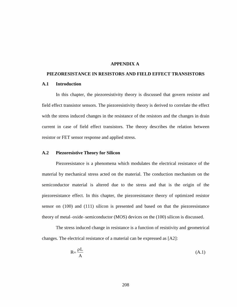
208
APPENDIX A
PIEZORESISTANCE IN RESISTORS AND FIELD EFFECT TRANSISTORS
A.1 Introduction
In this chapter, the piezoresistivity theory is discussed that govern resistor and
field effect transistor sensors. The piezoresistivity theory is derived to correlate the effect
with the stress induced changes in the resistance of the resistors and the changes in drain
current in case of field effect transistors. The theory describes the relation between
resistor or FET sensor response and applied stress.
A.2 Piezoresistive Theory for Silicon
Piezoresistance is a phenomena which modulates the electrical resistance of the
material by mechanical stress acted on the material. The conduction mechanism on the
semiconductor material is altered due to the stress and that is the origin of the
piezoresistance effect. In this chapter, the piezoresistance theory of optimized resistor
sensor on (100) and (111) silicon is presented and based on that the piezoresistance
theory of metal–oxide–semiconductor (MOS) devices on the (100) silicon is discussed.
The stress induced change in resistance is a function of resistivity and geometrical
changes. The electrical resistance of a material can be expressed as [A2]:
A
LR
(A.1)

209
In (A.1) ρ is the resistivity, L is the length and A is the average cross-sectional
area. The normalized change is resistance of a material due to small fractional changes in
stress can be defined by
A
A
L
L
R
R (A.2)
For resistors made of metal the change in geometrical dimensions in L and A are
main reason for the change in resistance of the material with stress whereas for
semiconductor resistors, the resistivity change is the dominant effect for the stress
induced changes with only a very small percent change is attributed to the change in
dimensions. The strain induced change in dimensions is negligible compared to the
resistivity change of the semiconductor material based on the fact that the resistance
change due to stress is large and also semiconductor materials have high elastic modulus.
The conductivity of a semiconductor material is a function of the carrier
concentrations, n and p, and carrier mobilities µn and µp.
pn pnq (A.3)
where q is the electric charge. For silicon those are doped either n type or p type, the
majority carriers are either electrons or holes. For example, for n type silicon the majority
carrier is electron and the concentration of electron is much higher that the concentration
of holes which is the minority carrier. So for n type silicon the minority carrier can be
neglected and the conductivity equation can be written as
nq n (A.4)

210
Now the resistivity of the material is inversely proportional to the conductivity,
hence based on Eq. (A.4) the normalized change in resistivity of the resistivity of the
material can be expressed as
(A.5)
Therefore the stress induced change in resistance of a semiconductor material can
be written in terms of the change in the mobility of the carrier.
R
R (A.6)
FigureA.1 Arbitrarily Oriented Silicon Filamentary Conductor
A.3 Piezoresistive Theory for Resistors
Silicon being an anisotropic material, the piezoresistance in silicon is also
anisotropic and depends on the wafer surface in which the resistor it is fabricated and also
the resistor direction on the surface.
A filamentary conductor as shown in Fig: A.1 is oriented arbitrarily with
reference to the unprimed axes x1 = [100], x2 = [010] and x3 = [001] that represents the

211
principal crystallographic directions of the cubic silicon crystal. The primed coordinate
system is at arbitrary angle with the unprimed coordinate system. For this filament in Fig.
A.1, the normalized change in resistance can be expressed in terms of the primed
components using [A1] [A2]:
...])T(T[
ml)(2nm)(2nl)(2
n)(m)(l)(R
R
221
654
23
22
21
(A.7)
where l′, m′ and n′ are the direction cosines of the conductor orientation with respect to
the primed axes x1′ , x2
′ and x3′ . παβ
′ (α,β = 1,2,….6) are thetemperature dependent
piezoresistance components along the off-axes, α1 and α2 are the temperature coefficients
of resistance and ΔT is the difference between the reference and measurement
temperature. If the principal coorodinate system [100], [010] and [001] is considered as
the reference axes, the cubic symmetry reduces the total number of unique
piezoresistance components from thirty six to three π11, π12and π44using the
transformation
TT (A.8)
where
44
44
44
111212
121112
121211
ij
00000
00000
00000
000
000
000
][ (A.9)
and the transformation matrix has the form

212
122112211221212121
233223322332323232
133113311331313131
33333323
23
23
22222222
22
22
11111121
21
21
mlmlnmnmnlnlnnmmll
mlmlnmnmnlnlnnmmll
mlmlnmnmnlnlnnmmll
ml2nm2nl2nml
ml2nm2nl2nml
ml2nm2nl2nml
]T[(A.10)
where l, m, n are the direction cosines of the primed coordinate system with respect to the
unprimed coordinate system and are given by
333
222
111
333231
232221
131211
ij
nml
nml
nml
aaa
aaa
aaa
]a[ (A.11)
The transformation matrix is reduced to 6 × 6 identity matrix when the unprimed
axes coincides with the primed axes. Thus Eq. (A.7) then becomes
...])T(T[
mnnllm[2n)]([
m)]([l)]([R
R
221
231312442
2211123311
23311122211
23322121111
(A.12)
Thus stress induced resistance change in an arbitrarily oriented silicon resistor is a
function of all six stress components, three unique piezoresistive coefficients and
temperature difference. By fabricating the resistor sensors in certain silicon wafer planes
that allows to take the advantage of the property of that wafer plane and as a result certain
stress components can be extracted from the resistance change measurements due to
stress.
A.4 Piezoresistance Equations for Silicon Wafer Planes
For an arbitrarily oriented resistor, Eq. (A.7) can be used to determine the change
in resistance for any wafer plane. In the current microelectronics industry, the commonly

213
used silicon wafer plane is (100) as depicted in Fig. A.2. We will discuss the resistance
change equations of resistors on (100) as well as on (111) wafer planes since the later
provides the advantage of extracting all six stress components by using optimized sensor
rosettes on that wafer surface [A1] [A2].
(100) Silicon
FigureA.2 (100) Silicon Wafer
Fig. A.2 shows the orientation of the principal (unprimed) and primed coordinate
system on (100) silicon wafer. Since it is a (100) silicon wafer so the direction
perpendicular to the surface is [001] direction. The [110] and [110] directions are the
unprimed axes which are at an angle 45˚ with the principal crystallographic axes and are
along and perpendicular to the primary flat of the wafer respectively.
In Fig. A.2, the direction cosines between the primed and the unprimed axes can
be obtained from Eq. (A.11)
100
02
1
2
1
02
1
2
1
nml
nml
nml
]a[
333
222
111
ij (A.13)
x1 110[ ]
[100]
(100) Plane
x2 110[ ]
x2 010[ ]
x1 100[ ]

214
Using theses direction cosines, the off-axis piezoresistive coefficients are
calculated using Eq. (A.8) and substituting that to Eq. (A.7) gives
T2sin
sin22
cos22
0,0R
0,0RT,R
R
R
1'121211
'3312
2'22
441211'11
441211
2'22
441211'11
441211
f
f
f
(A.14)
where l′ = cosφ, m′ = sinφ and n′ = 0 and angle ϕ represents the angle between the x'1
- axis and the resistor orientation. From Eq. (A.14) it is evident that, due to the absence of
σ'13 and σ '23in the equation, a sensor rosette on (100) silicon can be used to measure four of
the six unique components of the stress state at a point on the surface of the silicon.
A four-element dual-polarity sensor rosette on (100) is shown in Fig. A.3 that is
optimized for reducing thermal errors in measurements. The rosette contains a 0-90o p-type
resistor pair and a +45o n-type resistor pair.
FigureA.3 A Four-Element Rosette for (100) Silicon
x [100]1
x [010]2
x« [110]1
x« [110]2
45
R1,p
R2,p
R4,nR3,n

215
Application of Eq. (A.14) to the four resistor orientations gives the following
relations between the resistance changes and the stresses at the rosette site, where πS =
(π11+ π12)and πD = (π11- π12) has been introduced for expressing the equations for
notational convenience,
T2R
R
T2R
R
T22R
R
T22R
R
n
1
'
33
n
12
'
12
n
D
'
22
'
11
n
S
4
4
n
1
'
33
n
12
'
12
n
D
'
22
'
11
n
S
3
3
p
1
'
33
p
12
'
22
p
44
p
S'
11
p
44
p
S
2
2
p
1
'
33
p
12
'
22
p
44
p
S'
11
p
44
p
S
1
1
(A.15)
(111) Silicon
The second common silicon crystal orientation used in semiconductor fabrication is
(111) material, and a general (111) silicon wafer is shown in Fig. A.4. The direction [111]
is at a perpendicular direction on the (111) silicon surface. The principal crystallographic
axes x1 = [100], x2 = [010], and x3 = [001] does not lie on this (111) wafer surface. In Fig.
A.4, the direction cosines between the primed and the crystallographic direction can be
obtained from Eq. (11) similar to that for shown for (100) silicon.
3
1
3
1
3
16
2
6
1
6
1
02
1
2
1
nml
nml
nml
]a[
333
222
111
ij (A.16)

216
The resistance change of an arbitrarily oriented in-plane resistor on the (111)
surface can be expressed in terms of the stress components resolved in this natural wafer
coordinate system as described below :
T2sinBBBB22
sinBB22BBB
cosBB22BBBR
R
1'1221
'1332
2'2332
'333
'221
'112
2'2332
'333
'222
'111
f
f
f
(A.17)
FigureA.4 (111) Silicon Wafer
whereϕ is again the angle between the x'1-axis and the resistor orientation. The B
coefficients
3
2B
6
5B
2B 441211
3441211
2441211
1
(A.18)
represent a set of linearly independent temperature dependent combined parameters that are
convenient for characterization of piezoresistance on the (111) surface. From Eq. (A.17) it
is evident that, a sensor rosette on (111) silicon can be used to measure all six unique
components of the stress state at a point on the surface of the silicon die due to the presence
of all 6 stress components in the equation.
f
[111]
(111) Plane
n
x1 110[ ]
x2 1 12[ ]

217
Figure A.5 Top: An Eight-Element Rosette for (1110) Silicon. Bottom: Microphotograph
of an Eight-Element Complete Stress State Sensor on (111) Silicon
The eight-element dual-polarity rosette on (111) silicon illustrated in Fig. 5
contains p-type and n-type sensor sets, each with resistor elements making angles of ϕ =
0, ±45, and 90 degrees with respect to the horizontal x'1-axis. This sensor has been
developed for measurement of the complete state of stress at points on the surface of a
packaged semiconductor die. It has been optimized to measure four stress components in
a temperature compensated manner, and the “B” coefficients can be measured using a
combination of uniaxial and hydrostatic testing
Repeated application of Eq. (A.17) to each of the piezoresistive sensing elements
leads to the expressions in Eq. (A.19) for the stress-induced resistance changes.
45
R4,n
R7,pR8,p
R1,n
R2,nR3,n
x [112]2
x [110]1
R6,p
R5,p
45

218
Superscripts n and p are used on the combined piezoresistive coefficients to denote n-type
and p-type resistors, respectively.
T +)B B( )B - B(22 + B + ) + (2
B + B =
R
R
T +)B B(22 + B + B + B = R
R
n112
n2
n113
n3
n233
n32211
n2
n1
2
2
n123
n3
n233
n322
n211
n1
1
1
T + )B B( )B B(22 B + ) + (2
B + B =
R
R
T +)B B(22 B + B + B = R
R
T + )B B( +)B B(22 + B + ) + (2
B + B =
R
R
T +)B B(22 + B + B + B = R
R
T +)B B( )B B(22 B+ ) + (2
B + B =
R
R
T +)B B(22 B + B + B = R
R
p112
p2
p113
p3
p233
p32211
p2
p1
8
8
p123
p3
p233
p322
p111
p2
7
7
p112
p2
p113
p3
p233
p32211
p2
p1
6
6
p123
p3
p233
p322
p211
p1
5
5
n112
n2
n113
n3
n233
n32211
n2
n1
4
4
n123
n3
n233
n322
n111
n2
3
3
(A.19)
A.5 Piezoresistive Theory for Field Effect Transistors (FETs)
Fig. A.6 shows a schematic of a field effect transistor where S is the source, D is
the drain and G is the gate of the transistor. It has been observed that the current in the
field effect transistor is controlled by the resistive channel region when the transistor is
functioned in strong inversion in either the linear or saturation regions of operation.
Therefore, the application of stress can change the resistance of the channel region in
strong inversion, hence can demonstrate the piezoresistive behavior similar to that of a
resistor along the channel region [A3][A4][A5]. As a result of the change in resistance of

219
the channel region, the drain current changes. Since the channel region is lightly doped so
the lightly doped values of the piezoresistive coefficients can be used for FET’s.
Figure A.6: Cross-section of a Field Effect Transistor
The drain-source current expression for NMOS and PMOS transistors in the
saturation region is shown in the following.
2n
DN GS TN n DS
KI V V (1 V )
2 (A.20)
2p
DP GS TP p SD
KI V V (1 V )
2 (A.21)
where Kn and Kpare the transconduction parameters that is defined as
L
W
TL
WCK
ox
oxnoxnn
(A.22)
L
W
TL
WCK
ox
oxnoxpp
(A.23)
where VTN and VTP are the NMOS and PMOS threshold voltages of the transistor, VGS is
the gate to source voltage, VDS is the drain to source voltage, oxC is the gate oxide
capacitance per unit area, μn and μp are the electron mobility and hole mobility
respectively, Toxis the oxide thickness, n
and p
are the channel length modulation
n+ n+
S DG
Gate
Oxide
Channel
p type substrate

220
parameters,εoxis the dielectric constant of the oxide layer and W and L are the width and
length of the channel, respectively. It is obvious from the above equation is that the stress
induced change in drain current of the transistor can be caused by modulation of the
mobility, threshold voltage or change in device dimensions.
It has been discussed by Bradley that the strain-induced device geometry changes
in silicon can be neglected since the modulation of channel-length and width W and L,
are generally small compared to the stress induced changes in carrier mobility which is an
order or two larger in magnitude than the dimensional changes [A4]. Therefore the
modulation in drain current in NMOS in the saturation region can be written as
disregarding the dimensional change terms
TN TN n DSD n n
D n TN GS TN n n DS
V V VI K2
I K V V V 1 V
(A.24)
Similar expression can be written for PMOS. The stress induced changes in
threshold voltage demonstrate that this quantity is independent of stress . Therefore the
variation in drain current can be conveniently expressed by neglecting the second term and
only considering the stress induced mobility variation term alone.
The CMOS optimized sensor consists of pairs of NMOS and PMOS transistors
with orthogonal channel orientations as shown in Fig. A.7. The resistive channels of PMOS
transistor pair is oriented along 0˚ and 90˚ and for NMOS along ± 45˚. For an arbitrary
stress state, the drain current through a MOSFET by neglecting the effect of threshold
voltage variation can be written as
1I
I
I1III D
D
DDDD (A.25)
where

221
R
R
(A.26)
Figure A.7 CMOS Sensor Rosette in (100) Silicon
The stress induced variation in mobility depend on the orientation of wafer surface
and the current direction through the channel of the MOS device. The normalized change in
drain current due to stress for a MOSFET on (100) silicon in strong inversion can be
written [5] as
)T(f2sin
sin22
cos22I
I
12D3312
222
44S11
44S
222
44S11
44S
D
D
f
f
f
(A.27)
Fig. A.8: PMOS (Left) & NMOS (Right) Sensor Circuits
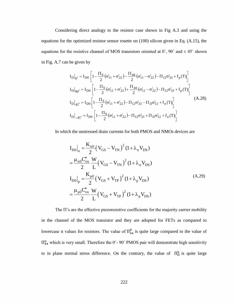
222
Considering direct analogy to the resistor case shown in Fig A.3 and using the
equations for the optimized resistor sensor rosette on (100) silicon given in Eq. (A.15), the
equations for the resistive channel of MOS transistors oriented at 0˚, 90˚ and ± 45˚ shown
in Fig. A.7 can be given by
)T(f
21II
)T(f2
1II
)T(f22
1II
)T(f22
1II
n12D33122211S
0D45D
n12D33122211S
0D45D
p3312221144
2211S
0D90D
p3312221144
2211S
0D0D
(A.28)
In which the unstressed drain currents for both PMOS and NMOs devices are
2n0D0 GS TN n DSn
2n0 oxGS TN n DS
2p0
D0 GS TP p DSp
2p0 ox
GS TP p DS
KI V V (1 V )
2
C WV V (1 V )
2 L
KI V V (1 V )
2
C WV V (1 V )
2 L
(A.29)
The П’s are the effective piezoresistive coefficients for the majority carrier mobility
in the channel of the MOS transistor and they are adopted for FETs as compared to
lowercase π values for resistors. The value of П44p
is quite large compared to the value of
П44n which is very small. Therefore the 0˚- 90˚ PMOS pair will demonstrate high sensitivity
to in plane normal stress difference. On the contrary, the value of ПDn is quite large

223
compared to the value of ПDP , therefore the ± 45˚ NMOS pair should be highly sensitive to
in-plane shear stress.
The MOSFET sensor for normal stress difference (PMOS) and for in-plane shear
stress (NMOS) are shown in Fig. A.8. One of the main considerations during the utilization
of piezoresistive stress sensors are the temperature compensation of the measured stress
terms since the temperature causes significant change in the measurements. On the (100)
surface, there are two basic temperature compensated rosette configurations. If the
normalized drain current variation for the orthogonal pair of devices are subtracted from
each other, which results in temperature compensated expressions and only the effect of
stress on the drain current remain.
12nD12
n12
n11
45D
45D
45D
45D
2211p44
0D
0D
90D
90D
22I
I
I
I
I
I
I
I
(A.30)
Due to the high values П44p
and ПDn , the orthogonal pair of PMOS devices is
elected for in-plane normal stress sensors and the orthogonal pair of NMOS devices is
taken as the in plane shear stress sensor.
A.6 Reference
[A1] Suhling, J. C. and Jaeger R.C. Silicon Piezoresistive Stress Sensors and Their
Application in electronic Packaging. IEEE Sensors Journal.pp. 14-30, 2001..
[A2] Bittle, D. A., Suhling, J. C., Beaty, R. E., Jaeger, R. C., and Johnson, R.W. .
Piezoresistive stress sensors for structural analysis of electronic packages,.
Journal of Electronic Packaging. 113(3): p. 203–215, 1991.

224
[A3] R. Ramani, "Piezoresistive Behaviour of MOSFET and FET-based Stress Sensor
Circuits," PhD Dissertation, Auburn University, 1996.
[A4] A. Bradley, “Piezoresistive Behavior of MOSFETS and MOS Circuits”’ PhD
Dissertation, Auburn University, 1999.
[A5] A. T. Bradley, R. C. Jaeger, J. C. Suhling, and K. J. O’Connor, “Stress sensitivity
of short-channel MOSFETs on (100) silicon,” IEEE Transaction Electron
Devices, vol. 48, no. 9, pp. 2009–2015, Sep. 2001.

225
APPENDIX B
Table B.1 Derivatives of Stress with respect to Resistor Values
p p n p p n p p n n n p p p n
1 2 1 3 1 3 2 3 2 1 2 1 2 3 1 2 3
1 1 2 2 3 3 4 4 5 5 6 6 7 7 8 8
p p p p p p n n
3 2 3 3 2 3 3 211
1 2 1 2
D B B B B B B B B B D B B B B B B
R R R R R R R R R R R R R R R R
B B B B B B B B0 0
2D 2D 2D 2D 2D
n n n n
3 3 2 3
1 2 1 2
p p p p p p n n n n n n
3 2 3 3 2 3 3 2 3 3 2 322
1 2 1 2 1 2 1 2
p p p p n n n n
1 2 1 2 1 2 1 233
2 2 2 2
p p p p n n
2 1 2 1 2 113
1 1
B B B B0 0
2D 2D 2D
B B B B B B B B B B B B0 0 0 0
2D 2D 2D 2D 2D 2D 2D 2D
B B B B B B B B0 0 0 0
2D 2D 2D 2D
B B B B B B2 2 20 0 0
8 D 8 D 8 D
n n
2 1
1 1
p p p p n n n n
2 1 2 1 2 1 2 123
1 1 1 1
p p p p n n n n
3 2 3 2 3 2 3 212
1 1 1 1
p p p p n n n n
3 2 3 2 3 2 3 211 22
1 1 1 1
B B20
8 D
B B B B B B B B2 2 2 20 0 0 0
8 D 8 D 8 D 8 D
B B B B B B B B0 0 0 0
2D 2D 2D 2D
B B B B B B B B
D D D D

226
Table B.2 Derivatives of Stress with respect to Temperature
o
n p p n
1 3 1 311
2
n p p n
1 3 1 322
2
n p p p n n
1 1 2 1 1 2
33
2
13
23
12
11 22
T Value (MPa/ C)
B B113
D
B B113
D
B B B B93.7
D
0 0
0 0
0 0
0 0
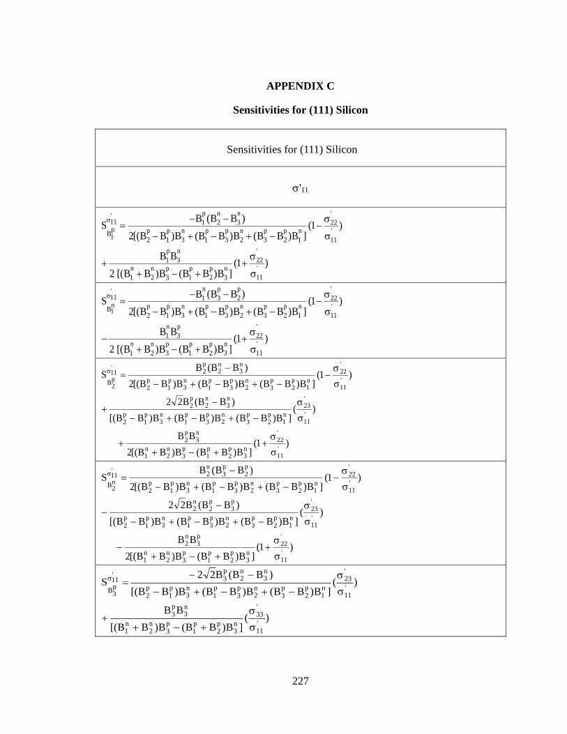
227
APPENDIX C
Sensitivities for (111) Silicon
Sensitivities for (111) Silicon
'11
p n n ''
11 1 2 3 22p p p n p p n p p n 'B1 2 1 3 1 3 2 3 2 1 11
p n '
1 3 22
n n p p p n '
1 2 3 1 2 3 11
B (B B )S (1 )
2[(B B )B (B B )B (B B )B ]
B B(1 )
2 [(B B )B (B B )B ]
n p p ''11 1 3 2 22n p p n p p n p p n 'B1
2 1 3 1 3 2 3 2 1 11
n p '
1 3 22
n n p p p n '
1 2 3 1 2 3 11
B (B B )S (1 )
2[(B B )B (B B )B (B B )B ]
B B(1 )
2 [(B B )B (B B )B ]
)1(]B)BB(B)BB[(2
BB
)(]B)BB(B)BB(B)BB[(
)BB(B22
)1(]B)BB(B)BB(B)BB[(2
)BB(BS
'11
'22
n3
p2
p1
p3
n2
n1
n3
p2
'11
'23
n1
p2
p3
n2
p3
p1
n3
p1
p2
n3
n2
p2
'11
'22
n1
p2
p3
n2
p3
p1
n3
p1
p2
n3
n2
p2
'11p2
B
)1(]B)BB(B)BB[(2
BB
)(]B)BB(B)BB(B)BB[(
)BB(B22
)1(]B)BB(B)BB(B)BB[(2
)BB(BS
'11
'22
n3
p2
p1
p3
n2
n1
p3
n2
'11
'23
n1
p2
p3
n2
p3
p1
n3
p1
p2
p3
p2
n2
'11
'22
n1
p2
p3
n2
p3
p1
n3
p1
p2
p2
p3
n2
'11n2
B
)(]B)BB(B)BB[(
BB
)(]B)BB(B)BB(B)BB[(
)BB(B22S
'11
'33
n3
p2
p1
p3
n2
n1
n3
p3
'11
'23
n1
p2
p3
n2
p3
p1
n3
p1
p2
n3
n2
p3
'11p3
B

228
)(]B)BB(B)BB[(
BB
)( ]B)BB(B)BB(B)BB[(
)BB(B22S
'11
'33
n3
p2
p1
p3
n2
n1
p3
n3
'11
'23
n1
p2
p3
n2
p3
p1
n3
p1
p2
p3
p2
n3
'11n3
B
'22
)1(]B)BB(B)BB[(2
BB
)1(]B)BB(B)BB(B)BB[(2
)BB(BS
'22
'11
n3
p2
p1
p3
n2
n1
n3
p1
'22
'11
n1
p2
p3
n2
p3
p1
n3
p1
p2
n3
n2
p1
'22p1
B
n p p n p' ''22 1 3 2 1 311 11n p p n p p n p p n ' n n p p p n 'B1
2 1 3 1 3 2 3 2 1 22 1 2 3 1 2 3 22
B (B B ) B BS (1 ) (1 )
2[(B B )B (B B )B (B B )B ] 2[(B B )B (B B )B ]
p n n ''
22 2 2 3 11p p p n p p n p p n 'B2 2 1 3 1 3 2 3 2 1 22
p n n ' p n '
2 2 3 23 2 3 11
p p n p p n p p n ' n n p p p n '
2 1 3 1 3 2 3 2 1 22 1 2 3 1 2 3 22
B (B B )S (1 )
2[(B B )B (B B )B (B B )B ]
2 2B (B B ) B B( ) (1 )
[(B B )B (B B )B (B B )B ] 2[(B B )B (B B )B ]
n p p ''22 2 3 2 11n p p n p p n p p n 'B2
2 1 3 1 3 2 3 2 1 22
n p p ' n p '
2 2 3 23 2 3 11
p p n p p n p p n ' n n p p p n '
2 1 3 1 3 2 3 2 1 22 1 2 3 1 2 3 22
B (B B )S (1 )
2[(B B )B (B B )B (B B )B ]
2 2B (B B ) B B( ) (1 )
[(B B )B (B B )B (B B )B ] 2[(B B )B (B B )B ]
)(]B)BB(B)BB[(
BB
)(]B)BB(B)BB(B)BB[(
)BB(B22S
'22
'33
n3
p2
p1
p3
n2
n1
n3
p3
'22
'23
n1
p2
p3
n2
p3
p1
n3
p1
p2
n3
n2
p3
'22p3
B
)(]B)BB(B)BB[(
BB
)(]B)BB(B)BB(B)BB[(
)BB(B22S
'22
'33
n3
p2
p1
p3
n2
n1
p3
n3
'22
'23
n1
p2
p3
n2
p3
p1
n3
p1
p2
p3
p2
n3
'22n3
B
σ'33
)(23.0)(]B)BB(B)BB[(2
)BB(BS
'33
'22
'11
'33
'22
'11
n3
p2
p1
p3
n2
n1
n2
n1
p1
B
'33p1

229
)(30.3)(]B)BB(B)BB[(2
)BB(BS
'33
'22
'11
'33
'22
'11
n3
p2
p1
p3
n2
n1
p2
p1
n1
B
'33n1
)(074.0)(]B)BB(B)BB[(2
)BB(BS
'33
'22
'11
'33
'22
'11
n3
p2
p1
p3
n2
n1
n2
n1
p2
B
'33p2
)(14.3)(]B)BB(B)BB[(2
)BB(BS
'33
'22
'11
'33
'22
'11
n3
p2
p1
p3
n2
n1
p2
p1
n2
B
'33n2
29.0)BB(]B)BB(B)BB[(2
B2S n
2n1n
3p2
p1
p3
n2
n1
p3
B
'33p3
29.1)BB(]B)BB(B)BB[(2
B2S
p2
p1n
3p2
p1
p3
n2
n1
n3
B
'33n3
σ'13
)
(]B)BB(B)BB(B)BB[(4
)BB(B2S
'13
'12
n1
p2
p3
n2
p3
p1
n3
p1
p2
n2
n1
p1
'13p1
B
)(]B)BB(B)BB(B)BB[(4
B)BB(2S
'13
'12
n1
p2
p3
n2
p3
p1
n3
p1
p2
n1
p2
p1
'13n1
B
]B)BB(B)BB(B)BB[(4
)22)(BB(B2
Sn1
p2
p3
n2
p3
p1
n3
p1
p2
'13
'12n
2n1
p2
'13p2
B
]B)BB(B)BB(B)BB[(4
)22)(BB(B2
Sn1
p2
p3
n2
p3
p1
n3
p1
p2
'13
'12p
1p2
n2
'13n2
B
]B)BB(B)BB(B)BB[(
)BB(BS
n1
p2
p3
n2
p3
p1
n3
p1
p2
n2
n1
p3
'13p3
B
]B)BB(B)BB(B)BB[(
)BB(BS
n1
p2
p3
n2
p3
p1
n3
p1
p2
p2
p1
n3
'13n3
B
σ'23
)(]B)BB(B)BB(B)BB[(8
)BB(B2S
'23
'22
'11
n1
p2
p3
n2
p3
p1
n3
p1
p2
n2
n1
p1
'23p1
B
)(]B)BB(B)BB(B)BB[(8
)BB(B2S
'23
'22
'11
n1
p2
p3
n2
p3
p1
n3
p1
p2
p2
p1
n1
'23n1
B
)24(]B)BB(B)BB(B)BB[(8
)BB(B2S
'23
'22
'11
n1
p2
p3
n2
p3
p1
n3
p1
p2
n2
n1
p2
'23p2
B

230
)24(]B)BB(B)BB(B)BB[(8
)BB(B2S
'23
'22
'11
n1
p2
p3
n2
p3
p1
n3
p1
p2
p1
p2
n2
'23n2
B
]B)BB(B)BB(B)BB[(
)BB(BS
n1
p2
p3
n2
p3
p1
n3
p1
p2
n2
n1
p3
'23p3
B
]B)BB(B)BB(B)BB[(
)BB(BS
n1
p2
p3
n2
p3
p1
n3
p1
p2
p2
p1
n3
'23n3
B
σ'12
]B)BB(B)BB(B)BB[(
B)BB(S
n1
p2
p3
n2
p3
p1
n3
p1
p2
p1
n2
n3
'12p1
B
]B)BB(B)BB(B)BB[(
B)BB(S
n1
p2
p3
n2
p3
p1
n3
p1
p2
n1
p3
p2
'12n1
B
)221(]B)BB(B)BB(B)BB[(
B)BB(S
'12
'13
n1
p2
p3
n2
p3
p1
n3
p1
p2
p2
n3
n2
'12p2
B
)221(]B)BB(B)BB(B)BB[(
B)BB(S
'12
'13
n1
p2
p3
n2
p3
p1
n3
p1
p2
n2
p2
p3
'12n2
B
)(]B)BB(B)BB(B)BB[(
B)BB(22S
'12
'13
n1
p2
p3
n2
p3
p1
n3
p1
p2
p3
n3
n2
'12p3
B
)(]B)BB(B)BB(B)BB[(
B)BB(22S
'12
'13
n1
p2
p3
n2
p3
p1
n3
p1
p2
n3
p3
p2
'12n3
B
σ'11- σ'22
]B)BB(B)BB(B)BB[(
)BB(BS
n1
p2
p3
n2
p3
p1
n3
p1
p2
n3
n2
p1
'22
'11p1
B
]B)BB(B)BB(B)BB[(
)BB(BS
n1
p2
p3
n2
p3
p1
n3
p1
p2
p2
p3
n1
'22
'11n1
B
)(]B)BB(B)BB(B)BB[(
)BB(B24
]B)BB(B)BB(B)BB[(
)BB(BS
'22
'11
'23
n1
p2
p3
n2
p3
p1
n3
p1
p2
n3
n2
p2
n1
p2
p3
n2
p3
p1
n3
p1
p2
n3
n2
p2
'22
'11p2
B

231
)(]B)BB(B)BB(B)BB[(
)BB(B24
]B)BB(B)BB(B)BB[(
)BB(BS
'22
'11
'23
n1
p2
p3
n2
p3
p1
n3
p1
p2
p3
p2
n2
n1
p2
p3
n2
p3
p1
n3
p1
p2
p2
p3
n2
'22
'11n2
B
)(]B)BB(B)BB(B)BB[(
)BB(B24S
'22
'11
'23
n1
p2
p3
n2
p3
p1
n3
p1
p2
n3
n2
p3
'22
'11p3
B
)( ]B)BB(B)BB(B)BB[(
)BB(B24S
'22
'11
'23
n1
p2
p3
n2
p3
p1
n3
p1
p2
p3
p2
n3
'22
'11n3
B
σ'11 + σ'22
]B)BB(B)BB[(
BBS
n3
p2
p1
p3
n2
n1
n3
p1
'22
'11p1
B
]B)BB(B)BB[(
BBS
n3
p2
p1
p3
n2
n1
p3
n1
'22
'11n1
B
]B)BB(B)BB[(
BBS
n3
p2
p1
p3
n2
n1
n3
p2
'22
'11p2
B
]B)BB(B)BB[(
BBS
n3
p2
p1
p3
n2
n1
p3
n2
'22
'11n2
B
)(]B)BB(B)BB[(
BB2S
'22
'11
'33
n3
p2
p1
p3
n2
n1
n3
p3
'22
'11p3
B
)(]B)BB(B)BB[(
BB2S
'22
'11
'33
n3
p2
p1
p3
n2
n1
p3
n3
'22
'11n3
B