Embed Size (px)
Citation preview
This content has been downloaded from IOPscience. Please scroll down to see the full text.
Download details:
IP Address: 134.151.40.2
This content was downloaded on 11/01/2014 at 11:36
Please note that terms and conditions apply.
The electronic band structure of Pb1-xSnxTe alloys. III. Implications for the Fermi surface of
SnTe
View the table of contents for this issue, or go to the journal homepage for more
1985 J. Phys. F: Met. Phys. 15 363
(http://iopscience.iop.org/0305-4608/15/2/011)
Home Search Collections Journals About Contact us My IOPscience
J. Phys. F: Met. Phys. 15 (1985) 363-376. Printed in Great Britain
The electronic band structure of Pb,,, Sn, Te alloys. 111: Implications for the Fermi surface of SnTe
He Yusheng and A D C Grassie Physics Laboratory, University of Sussex, Brighton BNI 9QH, UK
Received 24 April 1984
Abstract. Band-structure parameters derived for Pb, -,Sn,Te in paper I of this series from a Shubnikov-de Haas study are shown to give good agreement with the carrier concentration dependence observed for the anisotropy and the transverse effective mass in p-type PbTe. The parameters are also capable of yielding the x dependence of the anisotropy of the Fermi surfaces in Pb,-,Sn,Te in the cubic phase at low temperatures. With regard to the band structures deduced for the rhombohedral phase of Pb, -,Sn,Te, these are found to be capable of explaining the hitherto unexplained de Haas-van Alphen measurements of SnTe at low carrier concentration. The complexity of the Fermi surface for such low-carrier- concentration SnTe is discussed.
1. Introduction
In the preceding papers in this series, hereafter referred to as papers I and 11, band- structure parameters for samples of Pb,-,Sn,Te with x=O.32 and 0.37 for the cubic and rhombohedral phases were derived from the orientation dependence of the Shubnikov-de Haas (SDH) effect at 4.2 K. They were obtained by fitting the six-band model of Dimmock (1971) to the cubic-phase data and the six-band model of Bangert (1981) to the rhombohedral-phase data. These parameters were found to form a consistent set and to agree reasonably with the range of parameters reported previously for the cubic phase. Additional temperature-dependent parameters were obtained from the experimental data relating to the changes in crystallographic structure at the cubic-rhombohedral phase transition and values for the electron-transverse-optic-phonon matrix element were derived from a fit to the temperature dependences reported for the energy gaps of IV-VI alloys. These additional parameters, when taken into account in the finite-temperature band- structure calculation of Bangert (1 984), gave good agreement with the variations observed with temperature in the cross-sectional areas and effective masses through the structural and band inversion transitions for the two alloys concerned.
However, the important question is whether the band-structure parameters obtained in this way have any relevance to other compounds in the Pb,-.Sn,Te system. We shall show in this paper that this is in fact the case.
In the case of Pb,-,Sn,Te in the cubic phase, in which nearly all of the Fermi-surface studies have been carried out to date, we will show that our band-structure parameters derived from the samples with x=O.32 and 0.37 fit a wide range of the data reported for these materials. Furthermore, by taking our parameters in conjunction with the Bangert
0305-4608/85/020363 + 14%02.25 0 1985 The Institute of Physics 363
364 He Yusheng and A D C Grassie
model we are able to resolve the long-standing problem of the nature of the Fermi surface in low-carrier-concentration SnTe.
2. Experimental data
In place of a detailed review of work on the Pb,-,Sn,Te system in the cubic and rhombohedral phases with normal and inverted band ordering, table 1 assembles for p-type material the experimental results which we will discuss in this paper. The vast range of work on PbTe itself is summarised in table 2, where the results are presented as a function of the carrier concentration for p-type material.
3. The band-structure properties of the whole Pb, -, Sn, Te system
From the experimental results of our six samples of Pb, --x Sn, Te, the band-structure models have been examined in papers I and I1 and the parameters have been established for both the cubic and the rhombohedral phases. Now we are in a position to extend our models to see if they can cover the whole range of x in Pb, -, Sn, Te. The discussion will be divided into three parts.
Table I . Experimental Fermi-surface parameters for p-type Pb, -,Sn,Te
Carrier Composition concentration Anisotropy, Effective mass. Y ( 1 0 ~ * ~ m - ? K m*Jmg Reference
0 3.0 13 0.036 i 0.002 Burke et a1(1970) 0.13 0.45 12.5 0.0197 Burke et a1 (1970) 0.18 0.03 I 11.8i 1 0.0142 i 0.002 0.18 0.059 11.8i 1 0.0 149 i 0.002 0.18 0.060 1 3 . 0 i 1 0.0149 i 0.002 1 0. I8 0.18
0.125 0.180
0'0157i0'002 } Dmitrievetal(1977) 0.0167 i 0.002 1 2 . 0 i I 11.3 i 1
Melngailis etal(1971) Melngailis et a1 (197 1) Burke et al(1970)
0.18 0.250 11.8 + 1 0.0177 i 0.003 0. I8 0.324 11.0* I 0.0 184 i 0.003 0.18 6.55 l I . 3 * 1 0.0398 i 0.005 0. I85 0.03 1 - 0.0 120 i 0.001 5 0.186 0.26 10.5 i 1.0 0.0160 i 0.001 5 0.19 0.43 - 0.0195 0.216 0.85 11.2 i 0.5 0.0225 i 0.0015 Melngailis et a1 (197 1) 0.25 0.67 12.0 0.02 Kawamura et a1 (1978) 0.30 1.3 1 1 0.0257 Burkeetal(1970) 0.310 0.22 10.5 i 1.0 0.0140 i 0.001 S Melngailis et a1 (197 1) 0.315 1.8 10.5 * 1.0 0.0275 i 0.002 Burke et a1 ( 1 970) 0.32 1.0 10.5 i 0.8 0.049 i 0.001 Paper I 0.35 2.86 9 . s 0.0298 Kawamura et a1 (1978) 0.40 1.2 10.5t 0.0246 Kawamura et a1 (1978) 1 .o 3.7 6 .2 t - Nishiyama (1 975) 1 .o 6.0 - 0.125 f 0.012 Savage er a1 (1972)
f Possibly in rhombohedral phase.
I
Band structure of Pb, -, Sn,Te allo-vs. I I I 3 6 5
Table 2. Experimental Fermi-surface parameters for p-type PbTe. Data from Thomson et ai (1971). Coste (1967) and Cuff er a/ (1962) are omitted following the suggestion of Jensen er al(1978).
Carrier concentration Anisotropy, F,,, Effective mass. (10’8cm--’) K U) mi/nio Reference
Band edge 0.2 0.3 0.37 0.40 0.5 1 0.57 0.92 1.3 2.0 2.14 2.3 3.0 3.5 4 6 6.2 7.3
1 1 45
14 * 2 12.2 14.5 I 2 T 1
12.5 T 2 1 2 1 I
-
1 3 1 1 1 2 * 1 13 I 2 C I 13
-
- 13.0 i- 0.5 13.5 0.5 13.5 * 0.5 Non-ellipsoid
- 3. I O
3.55
6.54 8.50
10.00
-
-
-
- - - 18.0 21.9 25.1 53.3
0.022 1 0.003 0.03 1 0.029 0.022 z 0.003 -
0.024 1 0.003
0.027 i 0.003
0.035 0.002
0.035 0.002 0.036 + 0.002 0.038 1 0.002 0.040 1 0.008 0.044 c 0.009 0.050 T 0.002 0.048 i 0.002 0.050 + 0.002 0.072 f 0.002
-
-
-
Cuff er ai ( I 964) Nii (1964) Stiles et ai ( 1962) Cuff e! a l ( 1961) Jensen et ai (1978) Cuffetal(1961) Jensen er ai (1978) Burke ( I 97 I ) Jensen er ai (1 978) Jensen er a / (1978) Schilz (1969) Jensen et al(1978) B u r k e e t d ( 1 9 7 0 ) Burke ( l971) Schilz (1969) Schilz (1969)
Jensen et ai (1978)
3.1. x = 0: the case of PbTe
All the band models used derive originally from the Mitchell-Wallis (1966) scheme which is based on the band structure of PbTe. Thus, there ought to be no problem in applying all the models to PbTe. In the past twenty years, Fermi-surface studies of the Pb, -, Sn, Te system have concentrated on this material and many results for the carrier-concentration dependence of the Fermi-surface anisotropy K and the effective mass m* are available. This enables us to test our models thoroughly.
We have already shown in 0 4 of paper I that in the ellipsoidal non-parabolic Kane model the anisotropy factor K , defined as the square of the ratio of the maximum and minimum cross-sectional areas of the Fermi surface, is determined by the direct conduction-valence band interaction parameters Q- and Q, as
K = (Amu /A, , , )’ =(e, le, 1’ which implies that K is unaffected in this model by variation of the carrier concentration. The Dimmock model (see equation (2) in paper I) gives different results. To reduce the complication of the explicit analytical expression for K in the Dimmock model, consider
A k i - + Bkg, ~ ( 1 -X)E,.
For the case of sample H32, X= 0.142 z 4. The dispersion relation of the Dimmock model at the Fermi level can then be simplified to read
XE,(E, + E , -Ck;- -Dk$, )=Q?kg, +Qfk;,
366 He Yusheng and A D C Grassie
and hence
h2E,(1 + 2E,/E,)-h2Ck:, my = X.
2Q: + ~ C E F X
Under the same assumptions, the anisotropy coefficient K has the form
m* my
(2Qi + ~ C X E F ) ( ~ E F + E , - Dk;,) (2Qt + 2DXEF)(2EF + Eg - Ck;,) *
K =L= m
Since Qf % XDEF and 2EF + E, 9 I Dk;, I + lCk:, 1, we have
Q' +CXE, K x K , s
Q f It is clear that for the Dimmock model the anisotropy factor K is not only dominated by Q, and Q,, but is also affected by the Fermi level E,, i.e. by the carrier concentration. Now, from table 2 in paper I, we find that C= -4.1 1 x 10-l2 meV cm2 to give meV cm2 and the Fermi energy is less than zero for the p-type material (EF < 0) ; hence K increases approximately linearly with increasing concentration. However, for n-type material the opposite will be true.
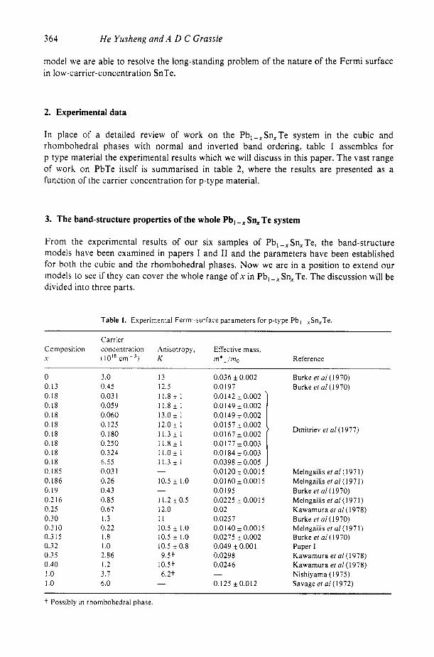
Rather than use the approximation above, we have computed the carrier-concentration dependence of the anisotropy factors K and K , for p-type material. This is plotted in figure 1 together with the experimental data taken from table 2. All the parameters used are exactly the same as in the case of sample H32, except that Q, is taken to have the value 54.0 x meV cm. The close agreement between theory and experiment suggests that this value of Q, is a good estimate and that the assumption is valid that all the other parameters A , B, C, D, Q, and Q- are carrier-concentration independent. The carrier- concentration dependence of the transverse effective mass in p-type PbTe is also examined
0 1 I 1 0 ' ~
t o r r ier concen t r n t I on, p ( cm- 3 ,
Figure 1. Carrier-concentration dependence of the anisotropy factor K (full line) and K, (broken line) of p-type PbTe. The curves are calculated from the six-band Dimmock model with the parameters taken from table 2 in paper I . The experimental data are taken from table 2 in this paper.
Band structure of Pb, -, Sn,Te alloys. III 367
ot I I I
Carrier concentrat ion p ( ~ r n - ~ ~ 10'8 1019
Figure 2. Carrier-concentration dependence of the transverse effective mass of p-type PbTe. The full curve is calculated from the six-band Dimmock model, with parameters as for figure I . The experimental data are taken from table 2.
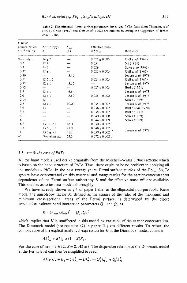
in figure 2. The agreement confirms that the band model used and its parameters are suitable for the case of PbTe, although there are small differences between the calculated m* and the experimental results. We attribute these to the mass enhancement due to electron-phonon interactions, and a value A = 0.15 0.05 was obtained which is consistent with the value deduced in 5 4 of paper 11.
3.2. 0 < x < I : rhe case of Pb, -, Sn, Te
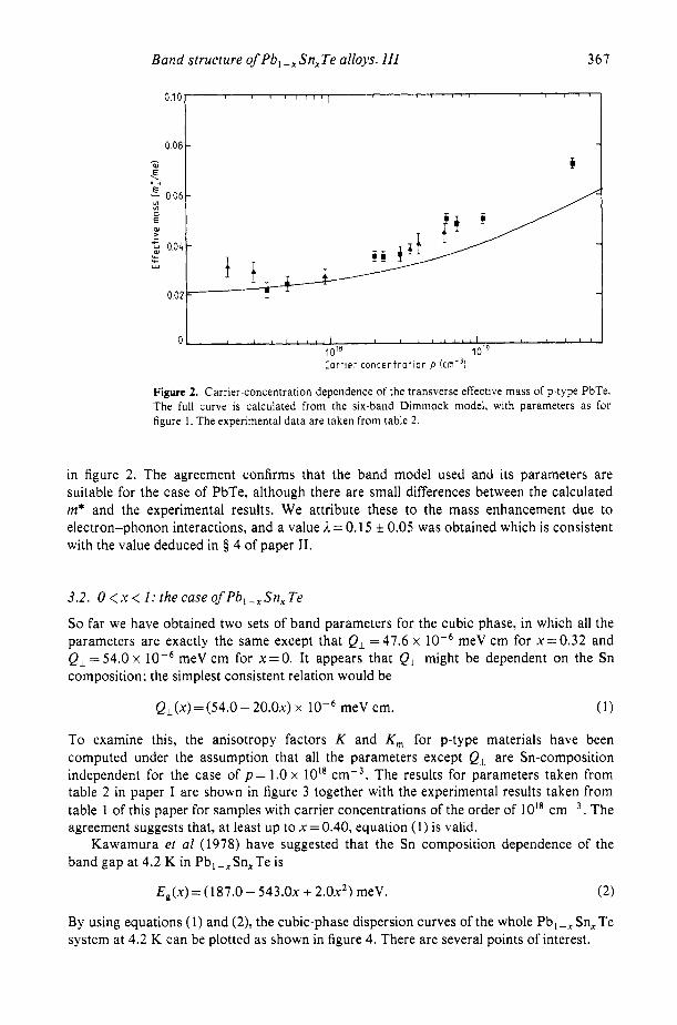
So far we have obtained two sets of band parameters for the cubic phase, in which all the parameters are exactly the same except that Q, =47.6 x meV cm for x=0.32 and Q, = 54.0 x meV cm for x = 0. It appears that Q, might be dependent on the Sn composition; the simplest consistent relation would be
QL(x)=(54.0-20.0x) x meV cm. (1)
To examine this, the anisotropy factors K and K , for p-type materials have been computed under the assumption that all the parameters except Q, are Sn-composition independent for the case of p = 1.0 x 10l8 ~ m - ~ . The results for parameters taken from table 2 in paper I are shown in figure 3 together with the experimental results taken from table 1 of this paper for samples with carrier concentrations of the order of 10'' cmP3. The agreement suggests that, at least up to x = 0.40, equation (1) is valid.
Kawamura et a1 (1978) have suggested that the Sn composition dependence of the band gap at 4.2 K in Pb,-,Sn,Te is
Eg(x)=(187.0-543.0x+ 2 . 0 ~ ~ ) meV. (2)
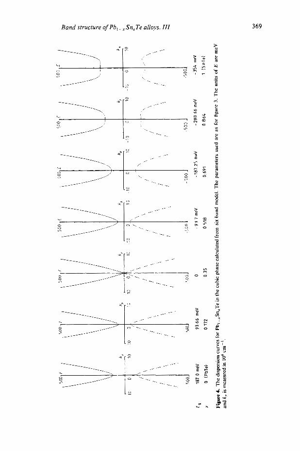
By using equations (1) and (2), the cubic-phase dispersion curves of the whole Pb, -, Sn, Te system at 4.2 K can be plotted as shown in figure 4. There are several points of interest.
368 He Yusheng and A D C Grassie
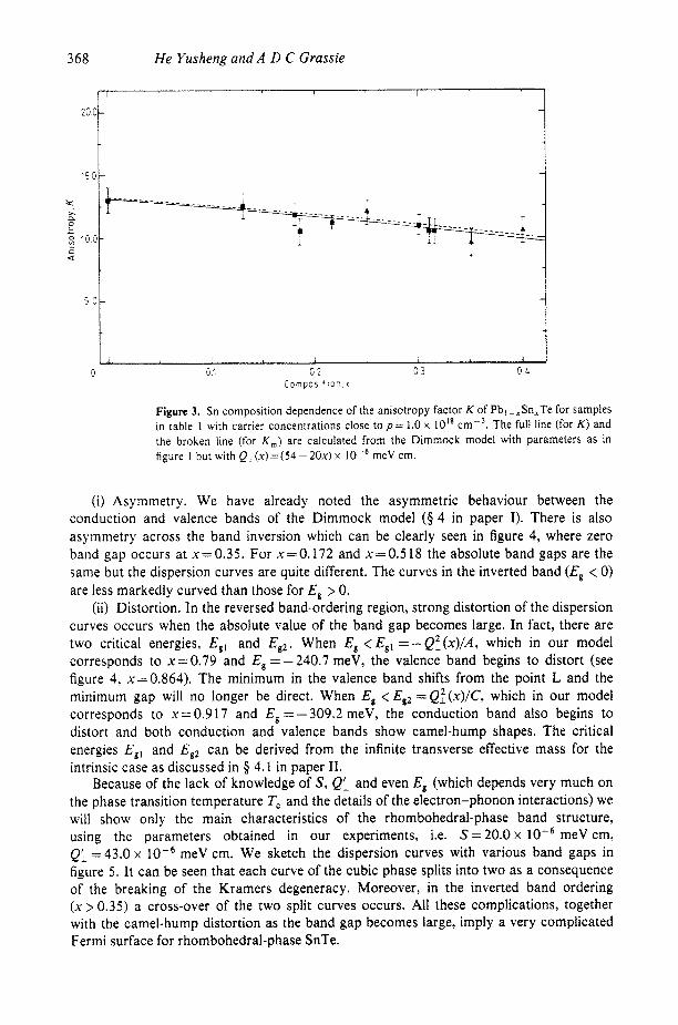
0 0 1 0 2 0 3 01, Compos1tion.x
Figure 3. Sn composition dependence of the anisotropy factor K of Pbl-,Sn,Te for samples in table 1 with carrier concentrations close t o p = 1.0 x lo'* ~ m - ~ . The full line (for K ) and the broken line (for K,) are calculated from the Dimmock model with parameters as in figure I but with QL(.~)=(54-20x)x meV cm.
(i) Asymmetry. We have already noted the asymmetric behaviour between the conduction and valence bands of the Dimmock model (5 4 in paper I). There is also asymmetry across the band inversion which can be clearly seen in figure 4, where zero band gap occurs at x=O.35. For x=O.172 and x=0.518 the absolute band gaps are the same but the dispersion curves are quite different. The curves in the inverted band (E, < 0) are less markedly curved than those for E , > 0.
(ii) Distortion. In the reversed band-ordering region, strong distortion of the dispersion curves occurs when the absolute value of the band gap becomes large. In fact, there are two critical energies, E,, and E g 2 . When E, < E,, = - Q : ( x ) / A , which in our model corresponds to x = 0.79 and E, = - 240.7 meV, the valence band begins to distort (see figure 4, x=0.864). The minimum in the valence band shifts from the point L and the minimum gap will no longer be direct. When E, < EB2 = Q: (x)/C, which in our model corresponds to x = 0.9 17 and E, = - 309.2 meV, the conduction band also begins to distort and both conduction and valence bands show camel-hump shapes. The critical energies E,, and E,, can be derived from the infinite transverse effective mass for the intrinsic case as discussed in 5 4.1 in paper 11.
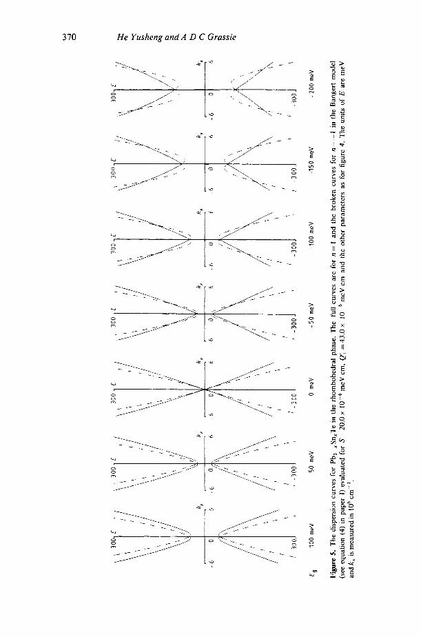
Because of the lack of knowledge of S , QI and even Eg (which depends very much on the phase transition temperature T, and the details of the electron-phonon interactions) we will show only the main characteristics of the rhombohedral-phase band structure, using the parameters obtained in our experiments, i.e. S = 20.0 x meV cm, Q: ~ 4 3 . 0 x meV cm. We sketch the dispersion curves with various band gaps in figure 5 . It can be seen that each curve of the cubic phase splits into two as a consequence of the breaking of the Kramers degeneracy. Moreover, in the inverted band ordering (x > 0.35) a cross-over of the two split curves occurs. All these complications, together with the camel-hump distortion as the band gap becomes large, imply a very complicated Fermi surface for rhombohedral-phase SnTe.
Band structure of Pb, -,Sn,Te alloys. 111 369
t-
h m
0
$ c r -
Ln m 0
W
K f .-
3 70 He Yusheng and A D C Grassie
h 0 0 N
f 0 tn
h 0
h 0 m
h
0 0
Band structure of Pb, --x Sn,Te alloys. I I I 371
3.3. x = l : thecaseofSnTe
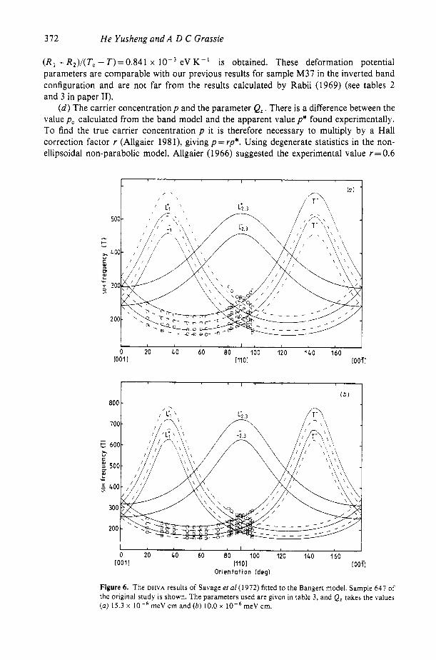
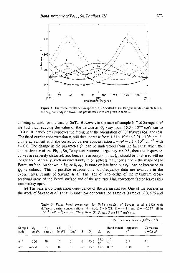
If we compare the dispersion curves of figure 4 for SnTe (x= 1) with the previously reported dispersion curves for SnTe calculated by different methods (Rabii 1969, Cohen and Tsang 1971), much agreement will be found. They all show a saddle point at L for both conduction and valence bands although there are slight differences in detail. The constant energy surface was found both by Rabii and by Cohen and Tsang to have threefold symmetry around ( 1 11) but in the present model there is only axial symmetry. Although the dispersion curves of the Bangert model for x = 1 reveal the main features of the band structure of SnTe, it is vital to see if that model of the rhombohedral band structure can effectively resolve the major mysteries about the Fermi surface of SnTe left over ten years ago, instanced by the de Haas-van Alphen (DHVA) data for SnTe obtained by Savage et a1 (1972). The four parallel frequency curves reported by Savage et a1 could imply four pieces of the Fermi surface and this is consistent with the T’ , T- , L’ and L- curves of our model if a domain structure is considered. Obviously, it is worth trying to fit the old data with the new model, using the parameters for samples L32 and M37. The fitted results are shown in figures 6 and 7; the parameters are listed in table 3 and can be seen to be essentially the same as those in table 5 in paper I. The following points are of interest relating to SnTe.
( a ) The band gap E,, Murase et a1 (1979) measured the band gap of samples of SnTe with p = 5.5 x I O l 9 cm-3 and 1.3 x 10,’ cmP3 , showing that the band gap decreases with decreasing temperature below T, = 100 K and that E, z 300 meV at about 4.2 K, which was taken as a parameter in our fitting procedure.
(b ) The tilt angle /I. Since for the cases of low and medium carrier concentration (p* < 3.5 x 10,’ cm-’, defined a s p * = 1/R,e as in Savage et a1 (1972)) the minima of the four curves are all located in the ( 1 1 1 ) direction, it appears that the L ‘apples’ of the SnTe Fermi surface are not tilted, i.e. /I=O. But this is not very clear for the samples of high carrier concentration (say p* = 6 x 10,’ ~ m - ~ ) since there are some indications (e.g., sample 652 of Savage et a1 (1972)) that the L ‘apples‘ may be tilted. More evidence is needed before a definite conclusion can be reached.
( c ) The parameters S and Q;, deformation potential 3 and energy shifts R , and R, . According to the finite-temperature Bangert model (see Q 2 in paper 11) we have
S = Q- sin 28 (3)
Q i = Q, COS 28 (4)
tan 28=22u/[lE,,I-(R1 + R,)] (5)
IE,I=[(lE,,/ + R I -R2) , + 4 Z ~ u ] ” ~ . (6)
For samples 647 and 670 of Savage et a1 (1972) we choose S= 6 x meV cm and Q: = 33.6 x meV cm. Since 6, + 33.6, = 34,, both the conditions Q, = 54.0- 2 0 . 0 ~ (equation ( I ) ) and S 2 + QF=Q; (equations (3) and (4)) are satisfied. In figure 3(b) in paper I1 we fitted equation (6) to the band-gap measurements of Murase et a1 (1979) and obtained the optical deformation potential Z = 1.27 eV, and the value ( R I -R2) / (Tc - T)=-0.528 x eV K- ’ which describes the shift of the conduction ( R I ) and the valence (R , ) bands due to the acoustical deformation potential Dd,” and the rhombohedral strain E d , since
R I , , =(3D3’ + D : ” ) E ~ + ~D:’E,
for the point T of the Brillouin zone. From equations (3), (4) and (5) a value of
372 H e Yusheng and A D C Grassie
(R, + R 2 ) / ( T c - 7')=0.841 x eV K- ' is obtained. These deformation potential parameters are comparable with our previous results for sample M37 in the inverted band configuration and are not far from the results calculated by Rabii (1969) (see tables 2 and 3 in paper 11).
( d ) The carrier concentrationp and the parameter Q, . There is a difference between the value pc calculated from the band model and the apparent value p* found experimentally. To find the true carrier concentration p it is therefore necessary to multiply by a Hall correction factor r (Allgaier 198 l), giving p = rp*. Using degenerate statistics in the non- ellipsoidal non-parabolic model, Allgaier (1 966) suggested the experimental value r = 0.6
I ,
0 20 40 60 80 100 120 140 160 [OOI I 11101 [OOTI
I I ,
0 20 40 60 80 100 120 140 160 I0011 I1101 rool1
Orientation (deg)
Figure 6. The DHVA results of Savage et a1 (1 972) fitted to the Bangert model. Sample 647 of the original study is shown. The parameters used are given in table 3, and Ql takes the values (a) 15.3 x meV cm and ( b ) 10.0 x meV cm.
Band structure of Pb,-,Sn,Te alloys. 111 373
0 20 40 60 BO 100 120 140 160 [ O O I 1 [no] [OOTI
0 r ien tot ion (degrees)
Figure 7. The D H V A results of Savage er a1 (1972) fitted to the Bangert model. Sample 670 of the original study is shown. The parameters used are given in table 3.
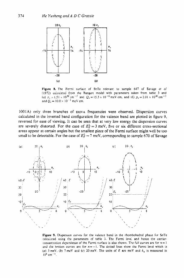
as being suitable for the case of SnTe. However, in the case of sample 647 of Savage et a1 we find that reducing the value of the parameter Q, (say from 15.3 x meV cm to 10.0 x lop6 meV cm) improves the fitting near the orientation of 90’ (figures 6(a) and (b)). The fitted carrier concentration p , will then increase from 1.5 1 x 10” to 2.01 x 10” cmp3 , giving agreement with the corrected carrier concentration p = rp* = 2.1 x 16’ cm-3 with r=0.6. The change in the parameter Q, can be understood from the fact that when the composition x of the Pb, --x Sn, Te system becomes large, say x > 0.8, then the dispersion curves are severely distorted, and hence the assumption that Q, should be unaltered will no longer hold. Actually, such an uncertainty in Q, reflects the uncertainty in the shape of the Fermi surface. As shown in figure 8, k,, is more or less fixed but kF, can be increased as Q, is reduced. This is possible because only low-frequency data are available in the experimental results of Savage et al. The lack of knowledge of the maximum cross- sectional areas of the Fermi surface and of the accurate Hall correction factor leaves this uncertainty open.
(e) The carrier-concentration dependence of the Fermi surface. One of the puzzles in the work of Savage et a1 is that in most low-concentration samples (samples 670, 676 and
Table 3. Fitted band parameters for SnTe samples of Savage ef a1 (1972) with different carrier concentrations. A = 6.06, B = 0.72 1, C = - 4.1 1 and D = -0.377 (all in I O - ’ * meV cm2) are used. The units of Q;,Qr and S are meV cm.
Carrier concentration (lo2’ cm-3)
Sample E, E , d E p Band model Apparent Corrected code (meV) (meV) (meV) (deg) S Qk Q z p e P* p = 0.6 p*
3.5 15.3 1.51
2.01 647 -300 70 17 0 6 33.6 2.1
670 -300 5 36 0 6 33.6 15.3 0.67 1.30 0.78
3 74 He Yusheng and A D C Grassie
28k, 28 k,
-28
( U )
kx 14 -14
-20
Ib)
kx 14
Figure 8. The Fermi surface of SnTe relevant to sample 647 of Savage el a1 (1972) calculated from the Bangert model with parameters taken from table 3 and (a) p C = 1 . 5 1 x 1020cm-3 and Q z = 1 5 . 3 x 1 0 - 6 m e V c m , and ( b ) p , = 2 . 0 1 x 1 0 2 0 c m - 3 and Q, = 10.0 x meV cm.
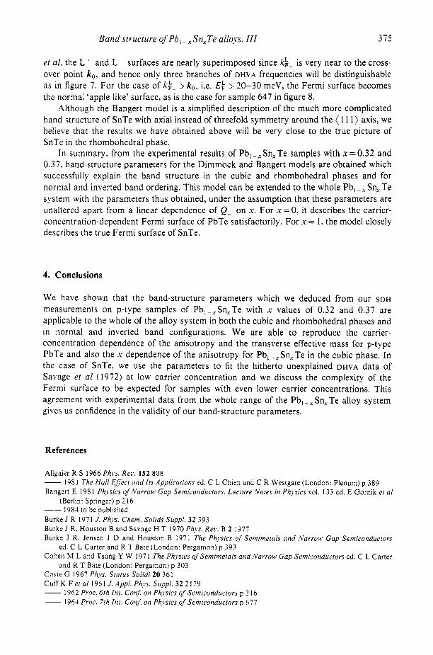
100 1 A) only three branches of DHVA frequencies were observed. Dispersion curves calculated in the inverted band configuration for the valence band are plotted in figure 9, reversed for ease of viewing. It can be seen that at very low energy the dispersion curves are severely distorted. For the case of E; = 3 meV, five or six different cross-sectional areas appear at certain angles but the smallest piece of the Fermi surface might well be too small to be detectable. For the case of E: = 7 meV, corresponding to sample 670 of Savage
-
-1 0
LOi€
~
30 I
2 0
I 1 -20
' I
\ \
\ \ / ' , ,/
3 o i 20 1 -20. i
10 IEF . , .. , . . , , .. ... , .. , . . . . . . . . . .. . . . . . . . . . . .... .. Y \ I
\ I \ /
\ i \ / \ /
'\
Figure 9. Dispersion curves for the valence band in the rhombohedral phase for SnTe calculated using the parameters of table 3. The Fermi level and hence the carrier- concentration dependence of the Fermi surface is also shown. The full curves are for n = 1 and the broken curves are for n=-1. The dotted lines show the Fermi level which is (a) 3 meV, ( b ) 7 meV and (c) 20 meV. The units of E are meV and k , is measured in lo6 cm- ' .
Band structure of Pb, -,Sn,Te alloys. 111 3 75
el al, the L' and L- surfaces are nearly superimposed since kkL is very near to the cross- over point k o , and hence only three branches of DHVA frequencies will be distinguishable as in figure 7. For the case of kk- > k o , i.e. E; > 20-30 meV, the Fermi surface becomes the normal 'apple-like' surface, as is the case for sample 647 in figure 8.
Although the Bangert model is a simplified description of the much more complicated band structure of SnTe with axial instead of threefold symmetry around the ( 11 1) axis, we believe that the results we have obtained above will be very close to the true picture of SnTe in the rhombohedral phase.
In summary, from the experimental results of Pb,-,Sn,Te samples with x=O.32 and 0.37, band-structure parameters for the Dimmock and Bangert models are obtained which successfully explain the band structure in the cubic and rhombohedral phases and for normal and inverted band ordering. This model can be extended to the whole Pb, -, Sn, Te system with the parameters thus obtained, under the assumption that these parameters are unaltered apart from a linear dependence of Q, on x. For x=O, it describes the carrier- concentration-dependent Fermi surface of PbTe satisfactorily. For x = 1, the model closely describes the true Fermi surface of SnTe.
4. Conclusions
We have shown that the band-structure parameters which we deduced from our SDH
measurements on p-type samples of Pb,-,Sn,Te with x values of 0.32 and 0.37 are applicable to the whole of the alloy system in both the cubic and rhombohedral phases and in normal and inverted band configurations. We are able to reproduce the carrier- concentration dependence of the anisotropy and the transverse effective mass for p-type PbTe and also the x dependence of the anisotropy for Pb, -, Sn, Te in the cubic phase. In the case of SnTe, we use the parameters to fit the hitherto unexplained DHVA data of Savage et a1 (1972) at low carrier concentration and we discuss the complexity of the Fermi surface to be expected for samples with even lower carrier concentrations. This agreement with experimental data from the whole range of the Pb,-,Sn,Te alloy system gives us confidence in the validity of our band-structure parameters.
References
Allgaier R S 1966 Phvs. Rec. 152 808 - 198 I The Hall ESfect and I t s .4pp/ications ed. C L Chien and C R Westgate (London: Plenum) p 389 Bangert E 1981 Phj.sics of ,\'arrow Gap Semiconductors, Leciure Notes in Physics vol. 133 ed. E Gornik er a1
__ 1984 to be published Burke J R 197 1 J . Phys. Chem. Solids Suppl. 32 393 Burke J R, Houston B and Savage H T 1970 Phys. Rev. B 2 1977 Burke J R, Jensen J D and Houston B 1971 The Physics of Semimetals and Narrou Gap Semiconductors
ed. C L Carter and R T Bate (London: Pergamon) p 393 Cohen M L and Tsang Y W 197 1 The Physics oJSemimerals and Narrow Gap Semiconductors ed. C L Carter
and R T Bate (London: Pergamon) p 303 Coste G 1967 Phys. Status Solidi 20 361 Cuff K F et a1 196 1 J . Appl. Phys. Suppl. 32 2 179 ___ 1962 Proc. 6th In t . ConJ on Physics of Semiconductors p 3 16 - 1964 Proc. 7th Int. ConJ on Physics qf Semiconduciors p 677
(Berlin: Springer) p 216
376 He Yusheng and A D C Grassie
Dimmock J 0 1971 The Physics ofSemimetals and Narrow Gap Semiconductors ed. C L Carter and R T Bate
Dmitriev A I et a1 1977 Sou. J . Low Temp. Phys. 3 213 Jensen J D, Houston B and Burke J R 1978 Phys. Rec. B 18 5567 Kawamura H et al 1978 The Application of High Magnetic Fields in Semiconductor Physics ed. J F Ryan
Melngailis J et al 1971 Phys. Rev. B 3 370 Mitchell D L and Wallis R F 1966 Phys. Rec. 151 581 Murase K et a1 1979 Physics of Semiconductors 1978 (Inst. Phys. Conf. Ser. 43) p 437 Nii R 1964 J . Phys. Soc. Japan 19 58 Nishiyama A 1975 J . Phj3s. Soc. Japan 40 47 1 Rabii S 1969 Phys. Rev. 182 821 Savage H T, Houston B and Burke J R 1972 Phys. Rev. B 6 2292 Schilz W 1969 J . Phys. Chem. Solids 30 893 Stiles P J et al 1962 Phys. Rec. Lett. 9 257 Thomson T E e f a1 1971 Phys. Rev. B 4 5 18
(London: Pergamon) p 3 19
(Oxford: Clarendon) p 170