Embed Size (px)
Citation preview
The impact of policy on technology innovation and cost reduction: a case study on crystalline silicon solar PV modules.
Working paper
November 2014
Authors: Ajay Gambhir1, Rob Gross2, and Richard Green3 1Grantham Institute, Imperial College London 2Centre for Energy Policy and Technology, Imperial College London 3Business School, Imperial College London

Table of Contents
Abstract................................................................................................................................. 5
1 Introduction ............................................................................................................... 6
2 Solar PV module manufacture ................................................................................... 8
2.1 Production of polysilicon ...................................................................................................... 9
2.2 Production of silicon wafers ................................................................................................. 9
2.3 Production of silicon cells ................................................................................................... 10
2.4 Module encapsulation ........................................................................................................ 11
3 Major innovations in PV module design and manufacture ................................................ 12
3.1 Polysilicon input prices ....................................................................................................... 12
3.2 Wafer manufacturing improvements .................................................................................. 12
3.3 Cell efficiency improvements ............................................................................................. 13
3.4 Cell encapsulation into modules ........................................................................................ 15
3.5 Automation and scale of cell and module manufacture ..................................................... 15
4 Major policy initiatives in solar PV module development and deployments ....................... 17
4.1 Summary of studies which quantify the impact of different factors on PV costs ............... 17
4.2 Identification of specific policies which have driven innovation and cost reduction ........... 24
5 Discussion ....................................................................................................................... 28
6 Conclusions ..................................................................................................................... 31
References ......................................................................................................................... 32

4
5
Abstract
The dramatic cost reduction in solar photovoltaic (PV) modules in recent years has
confounded expectations. Solar electricity generation cost is now approaching grid-parity,
with modules now costing less than $1/Wp. A key question is the extent to which different
policies have driven cost reductions, particularly when considering the different phases of
solar PV research, development, demonstration and deployment (RDD&D). Focusing on
crystalline silicon (c-Si) solar modules, which have dominated the PV market for several
decades, this study first reviews the quantitative (primarily statistical) evidence on drivers of
PV module price reductions, before considering more qualitatively which policies dominated
during periods of rapid innovation and cost reduction. Following c-Si modules’ early period of
space cell development, the mid-1970s saw the beginning of a dramatic period of innovation
in module design and manufacture, in large part driven by the US Jet Propulsion
Laboratory’s Flat-Plate Solar Array project, which achieved a more than five-fold reduction in
module production costs and which helped establish module designs not significantly
different to those produced today. Subsequently, increased demonstration and deployment
support activities helped to establish larger scale, more automated, lower cost
manufacturing, helping to achieve the current sub-$1/Wp production cost which has made
many reconsider the economics of PV. This story indicates that at relatively early stages of
technology development, governments should support targeted activities to achieve market-
ready designs, paving the way for subsequent deployment support to stimulate scale-up and
innovation in manufacturing, which could achieve equally if not more dramatic cost
reductions in the technology.
6
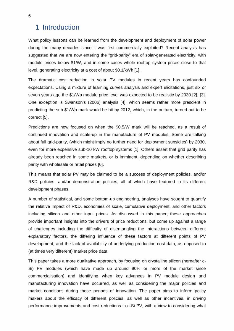
1 Introduction
What policy lessons can be learned from the development and deployment of solar power
during the many decades since it was first commercially exploited? Recent analysis has
suggested that we are now entering the “grid-parity” era of solar-generated electricity, with
module prices below $1/W, and in some cases whole rooftop system prices close to that
level, generating electricity at a cost of about $0.1/kWh [1].
The dramatic cost reduction in solar PV modules in recent years has confounded
expectations. Using a mixture of learning curves analysis and expert elicitations, just six or
seven years ago the $1/Wp module price level was expected to be realistic by 2030 [2], [3]. One exception is Swanson’s (2006) analysis [4], which seems rather more prescient in
predicting the sub $1/Wp mark would be hit by 2012, which, in the outturn, turned out to be
correct [5].
Predictions are now focused on when the $0.5/W mark will be reached, as a result of
continued innovation and scale-up in the manufacture of PV modules. Some are talking
about full grid-parity, (which might imply no further need for deployment subsidies) by 2030,
even for more expensive sub-10 kW rooftop systems [1]. Others assert that grid parity has
already been reached in some markets, or is imminent, depending on whether describing
parity with wholesale or retail prices [6].
This means that solar PV may be claimed to be a success of deployment policies, and/or
R&D policies, and/or demonstration policies, all of which have featured in its different
development phases.
A number of statistical, and some bottom-up engineering, analyses have sought to quantify
the relative impact of R&D, economies of scale, cumulative deployment, and other factors
including silicon and other input prices. As discussed in this paper, these approaches
provide important insights into the drivers of price reductions, but come up against a range
of challenges including the difficulty of disentangling the interactions between different
explanatory factors, the differing influence of these factors at different points of PV
development, and the lack of availability of underlying production cost data, as opposed to
(at times very different) market price data.
This paper takes a more qualitative approach, by focusing on crystalline silicon (hereafter c-
Si) PV modules (which have made up around 90% or more of the market since
commercialisation) and identifying when key advances in PV module design and
manufacturing innovation have occurred, as well as considering the major policies and
market conditions during those periods of innovation. The paper aims to inform policy
makers about the efficacy of different policies, as well as other incentives, in driving
performance improvements and cost reductions in c-Si PV, with a view to considering what
7
lessons could be applicable to other, more novel forms of PV, or to other low—carbon
energy technologies more generally.
The approach combines a review of literature covering the history of PV development, the
impact of policies on innovations and cost reductions in c-Si PV (and PV more generally)
and the views of industrial and academic experts involved in the development of c-Si PV
technology since the 1970s (see Acknowledgements section).
The paper is set out in 6 sections: Section 2 briefly describes the major steps in c-Si PV
module manufacture; Section 3 discusses the major innovations and cost reductions
achieved in each stage of the process; Section 4 discusses the role of policy and other
incentives in achieving these innovations; Section 5 discusses the relationship between
innovations and policy and non-policy drivers, and suggests lessons that this provides for
future PV and other low-carbon technology development; Section 6 concludes.
8
2 Solar PV module manufacture
A crystalline silicon solar PV module is essentially a thin wafer of silicon connected to two
electrodes, encapsulated in weather-proof materials. When light strikes the module, some of
the photons in the light are absorbed by the silicon, freeing electrons from the silicon bonds
and allowing them to travel through the silicon towards an electrode. An internal electrical
field exists within the silicon wafer as a result of a “p-n” junction, which separates two layers
of silicon that have been doped with boron and phosphorous respectively, giving them
different propensities to attract and release electrons. This field helps to separate the freed
electrons and the positively charged “holes” that they leave behind, before they can
recombine. The field drives electrons and holes to opposite electrodes connected to the
wafer, from where they enter an external circuit and do electrical “work” (e.g. in lighting and
appliances).
The module efficiency (i.e. the degree to which sunlight energy incident on the module is
converted to electrical energy) is improved by ensuring the maximum possible light reaches
the silicon wafer, which means the wafer surface must not be reflective, and also that the
wafer is sufficiently thick that light does not travel through it without most being absorbed. In
addition, efficiency is improved by ensuring that electrons and holes do not recombine
before they reach the electrodes. Recombination commonly occurs where there are
impurities in the silicon, particularly at silicon crystal grain boundaries where the silicon wafer
consists of many individual silicon crystals (as in multicrystalline silicon) as opposed to a
single crystal (as in monocrystalline silicon), and also where the metal electrodes are
connected to the wafer.
Many of the principal innovations in cell design have resulted in less reflective surfaces,
more absorption of light entering the wafer, and lower recombination rates of electrons and
holes. Other major innovations have resulted in cost reductions through cheaper production
of silicon, using less silicon to make a cell, and the development of larger scale, more
automated and ultimately cheaper processes to produce cells.
There are 4 major steps in the manufacture of c-Si solar PV modules, as shown in Figure 1,
and described in sections 2.1-2.4.
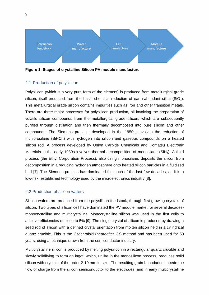
9
Figure 1: Stages of crystalline Silicon PV module manufacture
2.1 Production of polysilicon
Polysilicon (which is a very pure form of the element) is produced from metallurgical grade
silicon, itself produced from the basic chemical reduction of earth-abundant silica (SiO2).
This metallurgical grade silicon contains impurities such as iron and other transition metals.
There are three major processes for polysilicon production, all involving the preparation of
volatile silicon compounds from the metallurgical grade silicon, which are subsequently
purified through distillation and then thermally decomposed into pure silicon and other
compounds. The Siemens process, developed in the 1950s, involves the reduction of
trichlorosilane (SiHCl3) with hydrogen into silicon and gaseous compounds on a heated
silicon rod. A process developed by Union Carbide Chemicals and Komatsu Electronic
Materials in the early 1980s involves thermal decomposition of monosilane (SiH4). A third
process (the Ethyl Corporation Process), also using monosilane, deposits the silicon from
decomposition in a reducing hydrogen atmosphere onto heated silicon particles in a fluidised
bed [7]. The Siemens process has dominated for much of the last few decades, as it is a
low-risk, established technology used by the microelectronics industry [8].
2.2 Production of silicon wafers
Silicon wafers are produced from the polysilicon feedstock, through first growing crystals of
silicon. Two types of silicon cell have dominated the PV module market for several decades-
monocrystalline and multicrystalline. Monocrystalline silicon was used in the first cells to
achieve efficiencies of close to 5% [9]. The single crystal of silicon is produced by drawing a
seed rod of silicon with a defined crystal orientation from molten silicon held in a cylindrical
quartz crucible. This is the Czochralski (heareafter Cz) method and has been used for 50
years, using a technique drawn from the semiconductor industry.
Multicrystalline silicon is produced by melting polysilicon in a rectangular quartz crucible and
slowly solidifying to form an ingot, which, unlike in the monosilicon process, produces solid
silicon with crystals of the order 2-10 mm in size. The resulting grain boundaries impede the
flow of charge from the silicon semiconductor to the electrodes, and in early multicrystalline
Modulemanufacture
Cellmanufacture
Wafermanufacture
Polysiliconfeedstock
10
silicon manufacture in the 1950s efficiencies of only around 1% were achieved, although
with slower cooling to achieve larger crystals, this increased to about 6% efficiency in the
early 1970s [10] and to closer to 15% (at least at the laboratory level) as a result of a
number of other improvements by the end of the 1970s (see Section 3.3 and Figure 2).
The solid silicon (either mono or multi crystalline) is then sawn into wafers, which results in
40-50% losses of material, known as kerf losses [11].
Ribbon silicon production techniques have been experimented with since the 1970s, and a
wave of R&D in these techniques in the 1990s led to ribbon silicon cells having a market
share of almost 6% in 2001. Although there are a variety of techniques, they share the
principle of pulling a solidifying multicrystalline film of silicon from molten silicon, with film
thicknesses towards 100 micrometres achieved [11]. Ribbon silicon production finished in
2013 [8] which makes it unlikely to play a major role in crystalline silicon production going
forward.
2.3 Production of silicon cells
Commercial cell manufacture starts by taking a doped wafer (normally p-type, doped with
boron during the crystal-growing phase). The as-cut wafers are etched in alkaline or acidic
solutions to remove crystal damage caused by the sawing process [12]. Moncrystalline
wafers which are grown with a (100) (which means flat) crystal surface orientation are
alkaline-etched resulting in a (111) (pyramidal) surface texture that increases light-trapping.
Multicrystalline wafers are acid etched to generate a rough, low reflection surface. The p-n
junction is then created by doping one wafer surface with a phosphorous compound (for
example H3PO4, POCl3, or PH3) and heating to a temperature of 900-1000°C to drive the
phosphorus into the silicon surface [8]. An antireflective coating is then added, normally
through a process called plasma-enhanced chemical vapour deposition (PECVD) of
hydrogenated silicon nitride, which also “passivates” multicrystalline silicon cells – this
means it lowers rates of recombination by hydrogenating free silicon bonds in the
multicrystalline structure, which are prime points for electron and hole recombination. A front
electrode is then added typically through screen printing of a silver paste, whose simplicity
and low-cost compensate for the lower efficiencies compared to more precise laser, vacuum
evaporation and photolithographic methods. Some cell designs use lower cost copper
contacts which are buried into laser-formed grooves or surface channels and provide a
better balance between low contact resistance to the silicon whilst minimising shading
losses of incoming light. An aluminium paste is screen printed onto the back of the wafer,
which as well as acting as a rear electrode, also helps to form a back surface “field” which
reduces recombination rates [12]. Advanced cell processes have additional steps, including
further front and rear surface passivation using for example silicon oxide [13].

11
2.4 Module encapsulation
Module manufacture consists of interconnecting cells using copper ribbons, and a lamination
process which consists of placing the connected wafers between sheets of EVA (Ethylene
vinyl acetate), a transparent polymer which after heat treatment bonds to a front glass layer
and a rear fluoropolymer layer. Modules are then typically set in aluminium frames for
mounting. Finally modules are tested and qualified [12].
12
3 Major innovations in PV module design and
manufacture
A number of innovations have led to efficiency improvements, more efficient and larger-scale
manufacturing of both material inputs and the modules themselves, and less material usage,
all contributing to cost reductions in crystalline silicon PV modules, as discussed in Sections
3.1-3.5.
3.1 Polysilicon input prices
Polysilicon prices fell fairly steadily from about $300/kg (in US$2002 prices) in the late 1970s
to about $40/kg in the early 2000s [3], [4] as a result of increased scale of production, the
introduction of new processes including fluidised bed reactor processes and gradual process
improvements [8].
With the PV industry growing at around 50% per year since 2000, polysilicon supply failed
to keep pace with the growing demand. In 2000 about 4,000 tonnes (metric) of silicon were
consumed in the production of PV, which grew to 30,000 tonnes by 2007. This compared to
about 2 million tonnes of metallurgical grade silicon for all purposes [7]. Polysilicon
production was dominated by silicon chip manufacturers from Japan, Korea and the USA
until the early 2000s, with relatively little value attached to the wafer production as it
constituted a small part of the overall cost of silicon chips used in microelectronics [8].
Following the price spike around 2008, market entry from several new companies led to
significant cost reductions in polysilicon, now produced specifically for PV cells, with prices
falling to around $20/kg in 2014 [14].
3.2 Wafer manufacturing improvements
A number of developments have occurred in wafer manufacture since the 1950s, including
the increase in Cz crystal rod diameters, larger crucible sizes for multicrystalline silicon
production, and faster sawing with lower kerf losses [8]. Wafer sizes have steadily reduced
from 300 micrometres to about 180-200, but even thinner wafers present new challenges in
handling to avoid breakages. Wafers were originally cut using inner diameter (ID) saws in a
process pioneered by the microelectronics industry, but replaced by multi-wire sawing in the
early-to-mid 1980s, with lower kerf losses, higher throughput, and the ability to saw thinner
wafers [11]. In addition, wafer areas have increased twofold over the period 1979 to 2006
[4], reducing the handling required for a given power output of module.
13
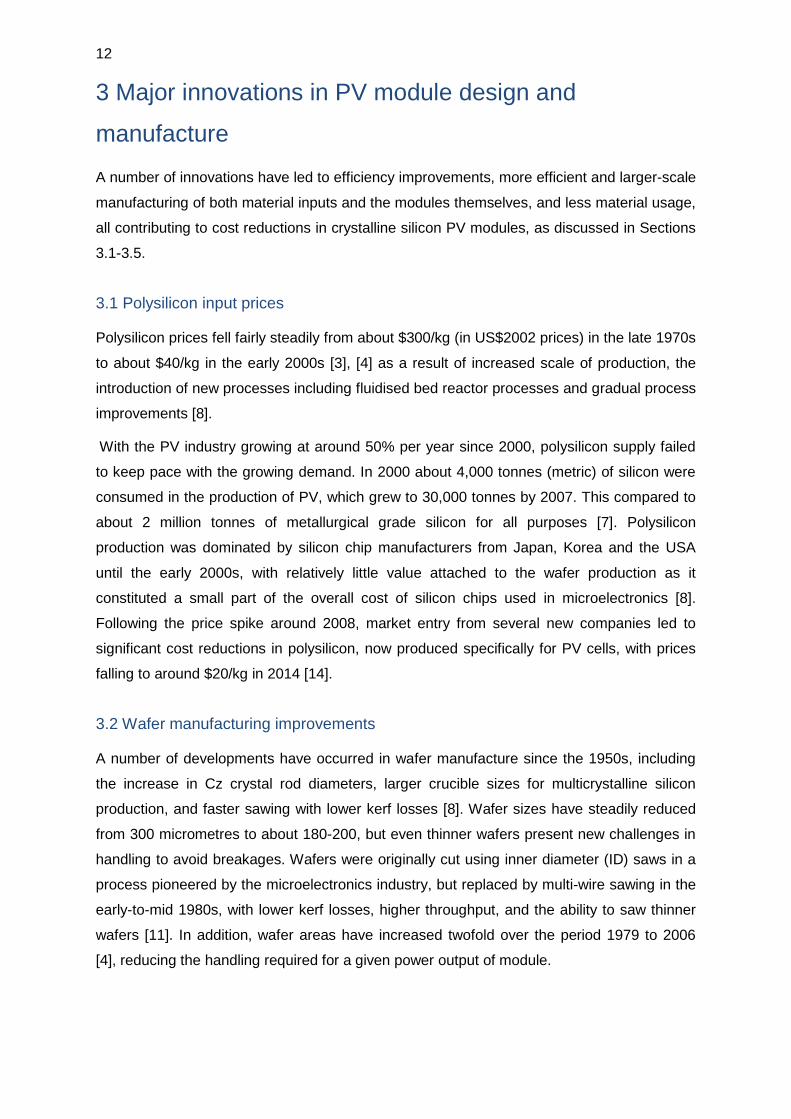
3.3 Cell efficiency improvements
Major innovations have occurred to cell designs which have increased cell efficiency and
therefore lowered the cost of modules in terms of their $/Wp figure. Figure 2 shows how the
maximum achieved laboratory efficiency of c-Si cells has developed over the past decades.
Figure 2: Evolution of mono and multicrystalline laboratory efficiencies [15]
Notes: Efficiency values are the highest reported in that year, under standard test conditions
There have been a number of drivers of laboratory-stage efficiency improvements, many of
which have eventually found their way into commercial cell manufacture. Wenham & Green
(1996) [16] outline three major periods of efficiency improvement. The first period of space
cell research in the late 1950s was driven by improvements in silicon crystal quality, as well
as using solid state diffusion to introduce dopants (boron and phosphorous) into the silicon
crystals – a superior technique compared to previous methods including helium ion
bombardment. Introduction of top metallic grid electrodes (as opposed to both electrodes at
the rear of the cell) shortened the distance travelled by electrons in the top n-type
conduction band to reach the top electrode, whilst allowing light through to the wafer.
The second period in the mid-1970s saw improvements resulting from the use of aluminium
as a rear contact, which served a “gettering” function (meaning it absorbed impurities from
the silicon) and also helped to create a back surface field to prevent recombination of
electrons and holes. In addition, further refinements to the top contacts were made (resulting
in finer, more closely spaced contacts), and titanium dioxide was introduced as an
antireflection coating. This period also saw the emergence of cells with pyramidal surfaces
0
5
10
15
20
25
30
1940 1950 1960 1970 1980 1990 2000 2010
Effic
ienc
y, % Mono (Triangles)
Multi (Squares)
Period 1 Period 2 Period 3
14
(etched in line with crystal planes inherent in the silicon crystal structure) to reduce incident
light reflection [16], [17].
Further experimentation from the mid-late 1980s led to further improved passivation at the
front of the cell by using a very thin layer of silicon oxide between the n-type silicon and front
electrodes, leading to the introduction of the Passivated Emitter Solar Cell (PESC). The
PERL (Passivated Emitter and Rear Locally diffused) cell introduced in the late 1980s/early
1990s is similar in design to the PESC cell, but with the rear aluminium replaced by a thin
silicon oxide layer (for passivation purposes, and to increase light reflection back into the
cell) and p+ doped regions in the silicon dioxide film. The mid-1980s also saw the
development of buried contact cells with copper plated front electrodes in laser-formed
grooves, to minimise contact resistance and shading losses [16]. These cells were
commercialised by BP Solar and sold from 1992-2008 (Mason, 2014).
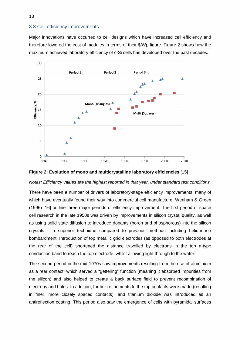
As can be seen from Figure 2, these three periods led to laboratory cell efficiencies
exceeding 20% (for multicrystalline cells) and 25% (for monocrystalline cells), made possible
by laboratory conditions for precise manufacture of prototype cells. Translating these gains
in efficiency to commercial cells has proven challenging, with efficiencies achieved in
commercial cell production considerably lagging those of laboratory cells, as shown in
Figure 3.
Figure 3: Average commercial module efficiency [18]
Notes: Average module efficiencies from survey of those in the market in given year. Best
module efficiencies now exceed 20% [19]
Nevertheless, the laboratory-stage efficiency improvements are gradually being incorporated
into cell manufacture, as techniques have been identified which can replicate the lab-stage
8
10
12
14
16
2000 2001 2002 2003 2004 2005 2006 2007 2008 2009 2010 2011 2012 2013 2014
Mod
ule
effic
einc
y, %
Mono Multi
15
process much faster and at larger-scale. Much of this innovation has come from learning-by-
doing in manufacturing.
3.4 Cell encapsulation into modules
The introduction of better lamination techniques has created more weather-resistant
modules, with glass and EVA lamination and Mylar/Tedlar fluoropolymer backings replacing
initial designs with silicone rubber lamination, achieving cost savings as well as
improvements in durability [20]. Many of these innovations were introduced in the early
1980s during the US Jet Propulsion Laboratory’s Flat Plate Array programme, and have
remained in module design to this day [21], as discussed in Section 4.
3.5 Automation and scale of cell and module manufacture
Many of the processes involved in module manufacture were performed by hand, when
factory capacities were up to ten MW per year until the early 1990s. At this stage most of the
equipment used had been developed in-house. Increased automation and increased factory
sizes led to cost reductions [4]. Throughput has also increased through the replacement of
batch processes with continuous processes, and additional cost savings have resulted from
the specialisation of equipment manufacturers now that the PV production market is large
enough. In the early decades cell manufacture borrowed heavily from the microelectronics
industry, using processes and equipment that were not specialised for PV production [11].
Figure 4 shows the major innovations in commercial c-Si PV module design and
manufacture since the 1950s breakthrough in cell efficiency.
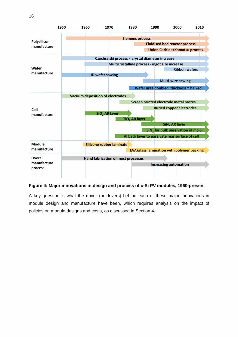
16
Figure 4: Major innovations in design and process of c-Si PV modules, 1960-present
A key question is what the driver (or drivers) behind each of these major innovations in
module design and manufacture have been, which requires analysis on the impact of
policies on module designs and costs, as discussed in Section 4.
1950 1960 1970 1980 1990 2000 2010
Siemens processPolysiliconmanufacture
Wafermanufacture
Czochralski process - crystal diameter increaseMulticrystalline process - ingot size increase
Modulemanufacture
Cellmanufacture
Fluidised bed reactor process
ID wafer sawingMulti-wire sawing
Ribbon wafers
Screen printed electrode metal pastesBuried copper electrodes
TiO2 AR layer
Union Carbide/Komatsu process
Vacuum deposition of electrodes
SiO2 AR layer
SiNX AR layerSiNX for bulk passivation of mc-Si
Al back layer to passivate rear surface of cell
Overallmanufactureprocess
EVA/glass lamination with polymer backing
Hand fabrication of most processesIncreasing automation
Silicone rubber laminate
Wafer area doubled, thickness ~ halved
17
4 Major policy initiatives in solar PV module
development and deployments
There have been a considerable number of policies across a range of countries to support
and promote the development and deployment of solar PV. In the last 10-15 years, several
countries have implemented market creation policies, most popular amongst them Feed-in-
Tariffs (FiTs), which offer guaranteed payments for each kWh of electricity generated by PV
systems. In addition, countries have experimented with capital subsidies including
investment tax credits and accelerated depreciation schemes, renewable energy certificates,
net metering and a range of other measures which have made solar PV a profitable
investment (see [22], [23] for a detailed summary of such market creation policies across
countries in which significant PV deployment has occurred).
There has also been continued public investment in solar PV R&D. However, Breyer et al
(2010) estimate that the public share of total R&D investment in solar PV has declined from
80% in the early 1980s to less than 10% in 2008, indicating that the vast majority of R&D is
now driven by private companies [24]. Furthermore, evidence suggests that R&D has
become a much less important public policy for solar PV overall than market creation
policies such as FiTs. Grau et al (2012) estimate that the value of PV R&D support
constitutes only about 1% of the value of deployment support in China and 3% of the value
of deployment support in Germany [25]. Before focusing on the specific drivers of c-Si PV
module design and manufacturing innovation (in Section 4.2), Section 4.1 first reviews the
quantitative evidence on the impact of policies on PV module prices.
4.1 Summary of studies which quantify the impact of different factors on PV costs
A number of statistical analyses have been undertaken to determine how different factors
have affected solar PV prices (as opposed to costs, where data is far less readily available).
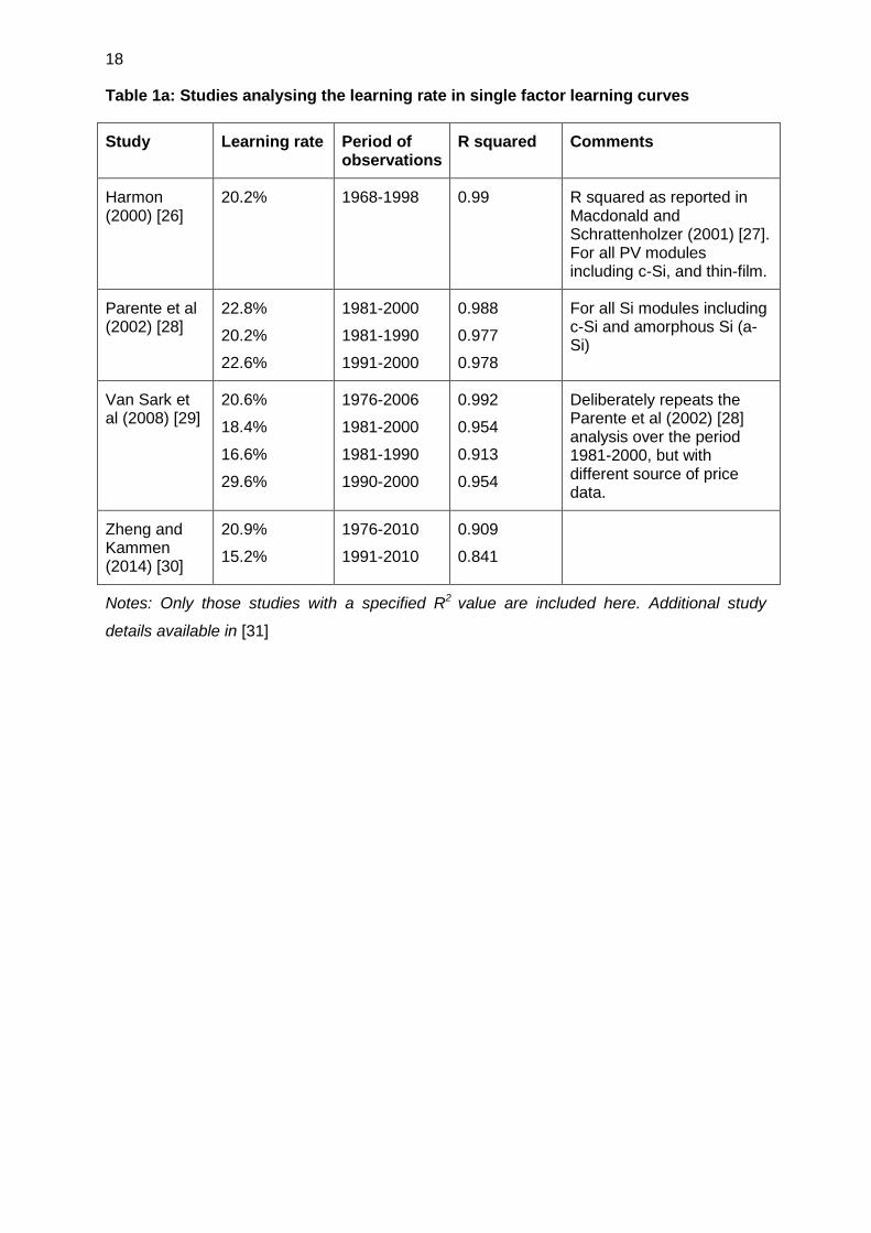
Table 1 summarises key findings from these studies. They have been categorised into three
groups: the first which analyses “learning-by-doing” as proxied by the impact of cumulative
deployment on PV module prices, which is the most common form of a single factor learning
curve; the second which adds R&D as a second factor affecting module prices; and the third
which analyses different factors such as economies of scale and silicon prices. All of these
studies relate to global c-Si PV prices and global factors unless otherwise indicated.
18
Table 1a: Studies analysing the learning rate in single factor learning curves
Study Learning rate Period of observations
R squared Comments
Harmon (2000) [26]
20.2% 1968-1998 0.99 R squared as reported in Macdonald and Schrattenholzer (2001) [27]. For all PV modules including c-Si, and thin-film.
Parente et al (2002) [28]
22.8%
20.2%
22.6%
1981-2000
1981-1990
1991-2000
0.988
0.977
0.978
For all Si modules including c-Si and amorphous Si (a-Si)
Van Sark et al (2008) [29]
20.6%
18.4%
16.6%
29.6%
1976-2006
1981-2000
1981-1990
1990-2000
0.992
0.954
0.913
0.954
Deliberately repeats the Parente et al (2002) [28] analysis over the period 1981-2000, but with different source of price data.
Zheng and Kammen (2014) [30]
20.9%
15.2%
1976-2010
1991-2010
0.909
0.841
Notes: Only those studies with a specified R2 value are included here. Additional study
details available in [31]
19
Table 1b: Studies analysing two-factor learning curves of learning-by-doing and learning-by-R&D
Study Learning-by-doing rate
Learning-by-R&D rate
Period of observations
R2 Comments
Miketa and Schrattenholzer (2004) [32]
17.5% 10.0% 1971-1997 0.80 Learning by R&D rate fixed at 10% (and assuming 2 year time lag and 3% annual R&D knowledge stock depreciation) to avoid multicolinearity between R&D and cumulative deployment data. R&D data is public spending. Data for all solar PV, not just c-Si.
Kobos et al (2006) [33]
18.4% 14.3% 1975-2000 0.990
Assumes a 3 year time lag between R&D and commercialisation, as well as an annual 10% depreciation of R&D stock. R&D data is public spending. Data for all solar PV, not just c-Si.
20
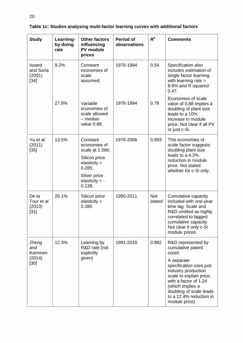
Table 1c: Studies analysing multi-factor learning curves with additional factors
Study Learning-by-doing rate
Other factors influencing PV module prices
Period of observations
R2 Comments
Isoard and Soria (2001) [34]
9.2%
27.8%
Constant economies of scale assumed;
Variable economies of scale allowed – median value 0.88.
1976-1994
1976-1994
0.54
0.78
Specification also includes estimation of single factor learning, with learning rate = 8.6% and R squared 0.47.
Economies of scale value of 0.88 implies a doubling of plant size leads to a 10% increase in module price. Not clear if all PV or just c-Si.
Yu et al (2011) [35]
13.5% Constant economies of scale at 1.066;
Silicon price elasticity = 0.285;
Silver price elasticity = -0.138.
1976-2006 0.993 This economies of scale factor suggests doubling plant size leads to a 4.2% reduction in module price. Not stated whether for c-Si only.
De la Tour et al (2013) [31]
20.1% Silicon price elasticity = 0.385
1990-2011 Not stated
Cumulative capacity included with one-year time lag. Scale and R&D omitted as highly correlated to lagged cumulative capacity. Not clear if only c-Si module prices.
Zheng and Kammen (2014) [30]
12.3%
Learning by R&D rate (not explicitly given)
1991-2010 0.882
R&D represented by cumulative patent count.
A separate specification uses just industry production scale to explain price, with a factor of 1.24 (which implies a doubling of scale leads to a 12.4% reduction in module price)
21
A number of observations can be made from these statistical analyses. There are a broad
range of learning-by-doing rates, which vary between 9 and 28% depending on the period of
analysis, the other factors included in the analysis, and the data sets used for the analysis.
The single-factor learning curves all show a learning rate close to 20%, which implies a 20%
reduction in c-Si PV module prices for each doubling of module installed capacity. However,
two analyses ([28], [29]) suggest that the single factor learning rate has been higher in the
period after 1990 when compared to the period before 1990. Zheng and Kammen’s (2014)
analysis appears to contradict this (with a lower learning rate over the period 1991-2010
compared to the whole period 1976-2010), but this includes the period after 2000 when
module prices actually increased as a result of polysilicon supply shortages [30]. As shown
in Section 3, many of the major design innovations in c-Si modules had already been made
by 1990, which could suggest that, following the emergence of this “dominant design” (as
Abernathy, Clarke and Utterback’s technology life-cycle model denotes it [36]), cost
reduction occurred at a faster rate because a large number of manufacturers began to scale-
up and refine production around a known technology (as opposed to experimenting with
several alternatives).
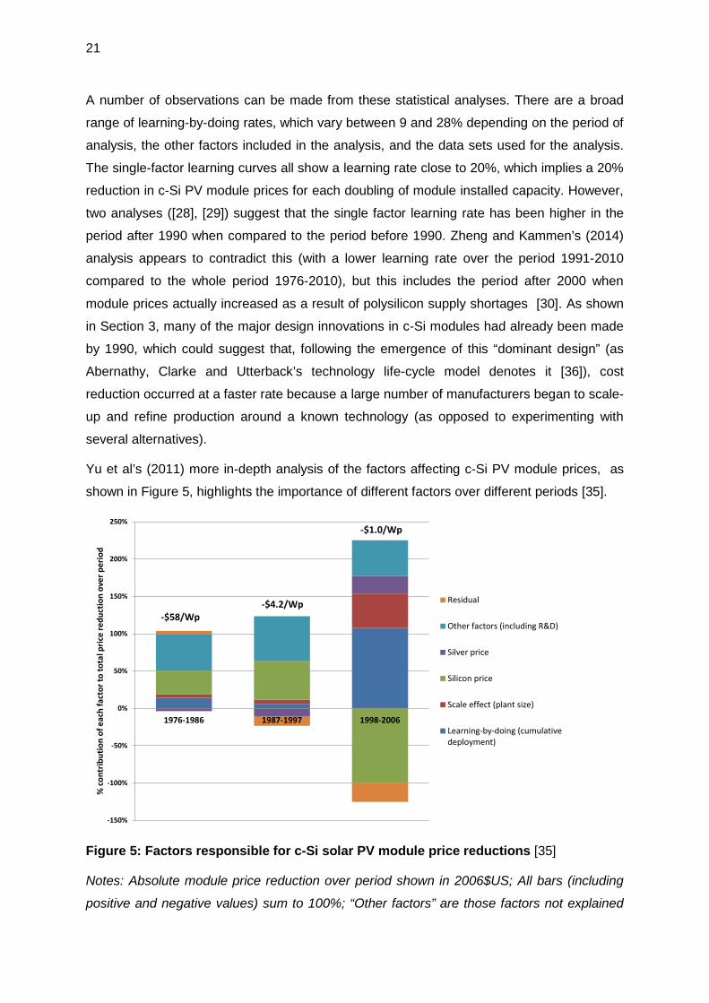
Yu et al’s (2011) more in-depth analysis of the factors affecting c-Si PV module prices, as
shown in Figure 5, highlights the importance of different factors over different periods [35].
Figure 5: Factors responsible for c-Si solar PV module price reductions [35]
Notes: Absolute module price reduction over period shown in 2006$US; All bars (including
positive and negative values) sum to 100%; “Other factors” are those factors not explained
-150%
-100%
-50%
0%
50%
100%
150%
200%
250%
1976-1986 1987-1997 1998-2006
% co
ntrib
utio
n of
eac
h fa
ctor
to to
tal p
rice
redu
ctio
n ov
er p
erio
d
Residual
Other factors (including R&D)
Silver price
Silicon price
Scale effect (plant size)
Learning-by-doing (cumulativedeployment)
-$58/Wp-$4.2/Wp
-$1.0/Wp
22
by the model; whereas the residual is the difference between the model and the actual PV
module price reductions.
In the periods 1976-1986 and 1987-1997 the primary drivers of module price reductions
were silicon input prices, and “other factors”, which Yu et al (2011) list as labour and capital
costs, subsidies, taxes and plant O&M costs, as well as R&D [35]. Although the authors do
not mention it in this context, this factor could account for the significant efficiency gains
experienced in commercial modules during this period, which may not have been picked up
in the learning-by-doing factor. The more recent period of analysis, 1998-2006, shows the
majority of price reductions coming from learning-by-doing and scale effects, although with
increased silicon prices offsetting much of these reductions, leading to relatively modest
absolute price reductions. It is likely that the significant focus on silicon production in
programmes such as the US Jet Propulsion Laboratory Flat Plate Array project of 1975-1985
(discussed in detail in Section 4.2) gave rise to the silicon price reductions experienced in
the first two periods shown, before supply bottlenecks sharply raised prices in the early
2000s [4].
The period following the mid-2000s, in which PV module prices fell to such an extent that
they “caught up” with the previous learning rate, has been examined by Zheng and Kammen
(2014), who find that a two-factor model including c-Si PV patent counts and market scale
best explains this late 2000s dramatic price reduction [30]. De la Tour et al (2013), by
contrast, find that a two-factor specification with cumulative deployment and silicon prices
provides the closest fit to prices over the period 1990-2011[31]. These two analyses,
identifying different explanatory factors, demonstrate the difficulty in producing a robust,
statistically-demonstrated assertion on the ultimate sources of change with regard to module
prices. Furthermore, neither of these specifications explicitly invokes the role of massive
Chinese module manufacturing expansion since the mid-2000s, which is discussed in further
detail in Section 4.2.
Aside from these statistical analyses, an engineering-based analysis by Nemet (2006)
attempts to explain c-Si PV module price using a detailed model of module costs accounting
for module efficiency, silicon usage, yield losses and plant scale [3]. Of these factors, plant
scale and efficiency improvements emerge as the two most important factors in driving down
PV module prices in the period 1980-2001, together accounting for about three-quarters of
all price reductions (manufacturing = 43%, efficiency = 31%). This does however rely on the
assumption that PV plant economies of scale match those from the semiconductor industry,
with a doubling of plant size resulting in a 12% reduction in module price – similar to the
industry economy of scale found statistically by Zheng and Kammen (2014) for the period
1991-2010 [30], but far greater than the 4% reduction rate found by Yu et al (2011) over the
period 1976-2006 [35], and even more divergent from the assertion by Isoard and Soria
23
(2001) that the PV industry experienced diseconomies of scale in the short run and constant
returns to scale in the long run [34]. This could imply that factors other than scale (and not
explained by Nemet’s analysis) were more significant.
As well as questioning the influence of different explanatory factors over different time
periods, it is also worth considering the degree to which the factors identified in the above
analyses are interrelated. Peters et al (2012) show that PV R&D (as represented by OECD
country patent counts) itself depends on deployment, with national R&D more strongly
dependent on PV capacity additions in the same continent than in other continents, implying
some form of geographical proximity effect [37]. Huo et al (2011) find that an increase in the
size of the PV module market in the USA, Germany and Japan led to innovation (again,
represented by patents granted) over the period 1992-2009 [38]. However, their analysis
also suggests that PV innovation caused market size increases in Germany and the USA
(the “cause” in both cases established by the Granger-causality statistical test). Bettencourt
et al (2013) find that PV patent counts are far better explained by a combination of public
R&D funding and market size, rather than by total (public and private) R&D funding [39].
They assert that public R&D funding is leveraged by market size, which allows more private
research and investments to add to and build upon this public R&D. Hoppmann et al (2013),
undertaking in-depth interviews with European, Chinese, Japanese and US firms and
experts in the PV industry, argue that over the period 2004-2010, when PV experienced very
high growth rates, policy-induced market growth led to an increase in R&D spending in
absolute terms, but the intensity of R&D (measured as R&D spend as a share of revenues)
fell, as a result of reduced exploration pressure, the need to focus management resources
on market expansion, and the increase in supply of manufacturing equipment focused on
producing the mature technology. These effects were most clearly shown by firms producing
more mature (c-Si) PV modules [40].
Analysis at a national level also suggests a complex interplay between factors. Watanabe et
al (2000) relate data on PV module production and prices in Japan to the R&D knowledge
stock (as measured by cumulative patents), temporal learning and production scale, over the
period 1976-1995 [41]. They find that price depends on production scale as well as
knowledge stock. By also demonstrating a statistical relationship between price reductions in
one year and PV production in the following year, they assert that there is a feedback loop
between PV production, R&D investment, and price reductions.
In summary, the single-factor learning curve analyses over multi-decadal periods of PV
evolution provide an apparently compelling relationship between capacity doubling and
roughly 20% module price reductions. But this learning rate varies significantly over distinct
decadal periods, with the 1980s seeing less dramatic price reductions than the 1990s, and
the 2000s seeing a slow-down as silicon prices rose, before once again falling in order to
24
“catch up” with the 20% learning curve. In each period there is evidence that different factors
(particularly silicon prices, and factors including R&D) have played a different role, which
suggests there is no intrinsic, fundamental causal relationship between deployment and
price reductions in the absence of other factors. Furthermore, the factors affecting module
prices are themselves interlinked, which suggests that the process of innovation and cost
reduction occurring in the PV module market is complex. This makes derivation of policy
lessons difficult as it does not indicate a clear strategy of how much R&D to invest in, as
opposed to deployment support.
Section 4.2 takes a more qualitative look at the major policies and market conditions during
the distinct periods of c-Si PV module design and manufacturing improvements, with a view
to identifying whether particular advances can be related to particular drivers.
4.2 Identification of specific policies which have driven innovation and cost reduction
Considering the major innovations in crystalline silicon PV in particular, a number of specific
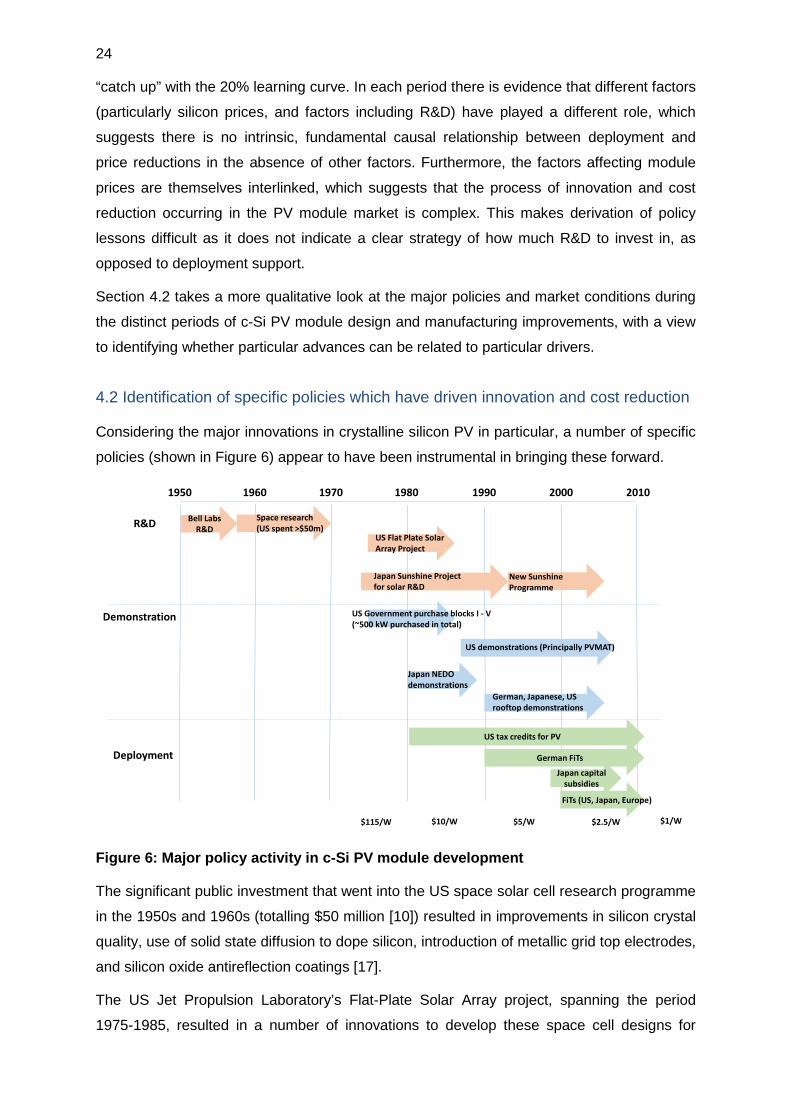
policies (shown in Figure 6) appear to have been instrumental in bringing these forward.
Figure 6: Major policy activity in c-Si PV module development
The significant public investment that went into the US space solar cell research programme
in the 1950s and 1960s (totalling $50 million [10]) resulted in improvements in silicon crystal
quality, use of solid state diffusion to dope silicon, introduction of metallic grid top electrodes,
and silicon oxide antireflection coatings [17].
The US Jet Propulsion Laboratory’s Flat-Plate Solar Array project, spanning the period
1975-1985, resulted in a number of innovations to develop these space cell designs for
1950 1960 1970 1980 1990 2000 2010
R&D
Demonstration
Space research(US spent >$50m)
US Government purchase blocks I - V(~500 kW purchased in total)
US demonstrations (Principally PVMAT)
Japan NEDOdemonstrations
German, Japanese, USrooftop demonstrations
DeploymentJapan capital
subsidies
German FiTs
US Flat Plate SolarArray Project
Japan Sunshine Projectfor solar R&D
New SunshineProgramme
Bell Labs R&D
US tax credits for PV
$115/W $10/W $5/W $2.5/W $1/W
FiTs (US, Japan, Europe)
25
terrestrial usage. The US Government’s block purchases of modules which accompanied
the project were associated with steady increases in cell efficiency (from around 5% in the
first purchase block in 1975-76, to about 10% by 1985). Successive blocks also helped to
field test and establish different module encapsulants, with silicone rubber giving way to
polyvinyl butyral (PVB) and eventually ethylene vinyl acetate (EVA) as a transparent
laminate for bonding the cells to glass on the front and fluoropolymers (such as Mylar and
Tedlar) on the back. More densely packed “quasi-square” wafers, multicrystalline square
wafers and screen printing also became established during this programme [17], [20].
Concurrent with the Flate-Plate Solar Array project was the “burst of laboratory activity” [17]
which brought about significant improvements in cell efficiency through better antireflection
coatings (based on titanium oxide rather than silicon oxide), aluminium backings to reduce
recombination, and the emergence of etching of silicon wafer surfaces to expose pyramidal
crystal surfaces which better absorbed incident light.
As O’Conner et al (2010) assert, “Modules improved so drastically from Block I (1976) to
Block V (1984) that the modules evaluated in Block V were not significantly different from
those used today.” [21]. By the middle of the 1980s commercial cells were being produced
with efficiencies of greater than 10%, with the laboratory knowledge to achieve cells with
greater than 20%, using passivating techniques which would eventually seep through to
commercial cell production and lead to c-Si module efficiencies today which range from 15-
20% [8].
During the 1980s itself an increased focus on demonstration projects allowed the field-
testing of a number of PV design aspects. In the USA, PVUSA was launched in 1986 as a
joint programme between the Department of Energy and numerous utilities, to demonstrate
utility-scale PV. PVMAT began in 1990, with the aim of reducing costs, PV Bonus in the
1990s with the aim of developing building applications, and TEAMUP in 1994, to provide
energy service provider applications. In Japan a number of demonstration programmes
aimed at testing grid connection and PV system monitoring were enacted in the 1980s and
early 1990s, including PV for Public Facilities in 1992, as well as the PV systems (roof
monitor) programme in 1994, which later became the Residential PV system demonstration
programme. The first demonstration programme in Germany was the Rational Use of Energy
and the Use of Renewable Energy Sources (REN) in 1988, to support R&D and
demonstration across a range of technologies. During the 1980s and 1990s German
municipalities and utilities installed several grid-connected systems, in which a large number
of different types of module were evaluated [42].
The mid-late 1990s heralded the period of deployment support policies. In 1997 in the USA
the Million Solar Roofs programme was launched (to be achieved by 2010). At the same
time, Federal programmes such as California’s PV Pioneer programme were introduced, to
26
trial 4kW rooftop systems in selected homes. In 1998 net metering laws were introduced in
the USA, which stimulated significant market growth. In Germany, the initial FiTs offered (in
the early 1990s) at 90% of retail electricity rates were not successful in stimulating the
market, but the much more generous rates in 1999, combined with the 100,000 roofs
programme, did stimulate rapid growth in the market [42]. Japan’s 1997 PV residential
system dissemination programme began with a 50% subsidy for residential rooftop systems,
with the subsidy rate declining as system prices fell [43]. Several other deployment support
policies have followed across the world, including notably generous tariffs (causing a boom
and bust, although with a recent market stabilisation) in Spain [44].
Any discussion of PV module price developments over recent years should of course also
include the role of Chinese manufacturers. Goodrich et al (2013) assert that the
considerable cost difference between Chinese and US-produced modules (analysing data
for the first half of 2012) is primarily the result of cheaper inputs due to scale, material
discounts, and equipment discounts, all resulting from scale-based advantages of larger
manufacturing plants, with typical US plants at 500MW per year, compared to plants
approaching 2GW per year in China [5]. These scale-based advantages in total provide a
$0.22/Wp advantage in Chinese PV module costs (at just under $0.75/Wp, compared to just
under $1/Wp in the USA) with the remaining discount the result of lower labour and financing
costs. The authors posit that the USA could achieve similar scale-based discounts to
achieve cost competitiveness with China in the long run, assuming that similar plant-based
production scale can be achieved. This scale effect approximates to a 9% reduction in
module cost for a doubling of plant size – an interesting comparator to the range of economy
of scale estimates discussed in Section 4.1 (which imply cost reduction factors from plant
size doubling ranging from a long-term value of 0% to 12%).
Considering all of these policies together, as well as the major innovations discussed in
Section 3, Figure 7 provides a high-level description of the progress made in c-Si PV module
manufacture over the past 5 decades, with a view to identifying the major drivers of cost
reductions.
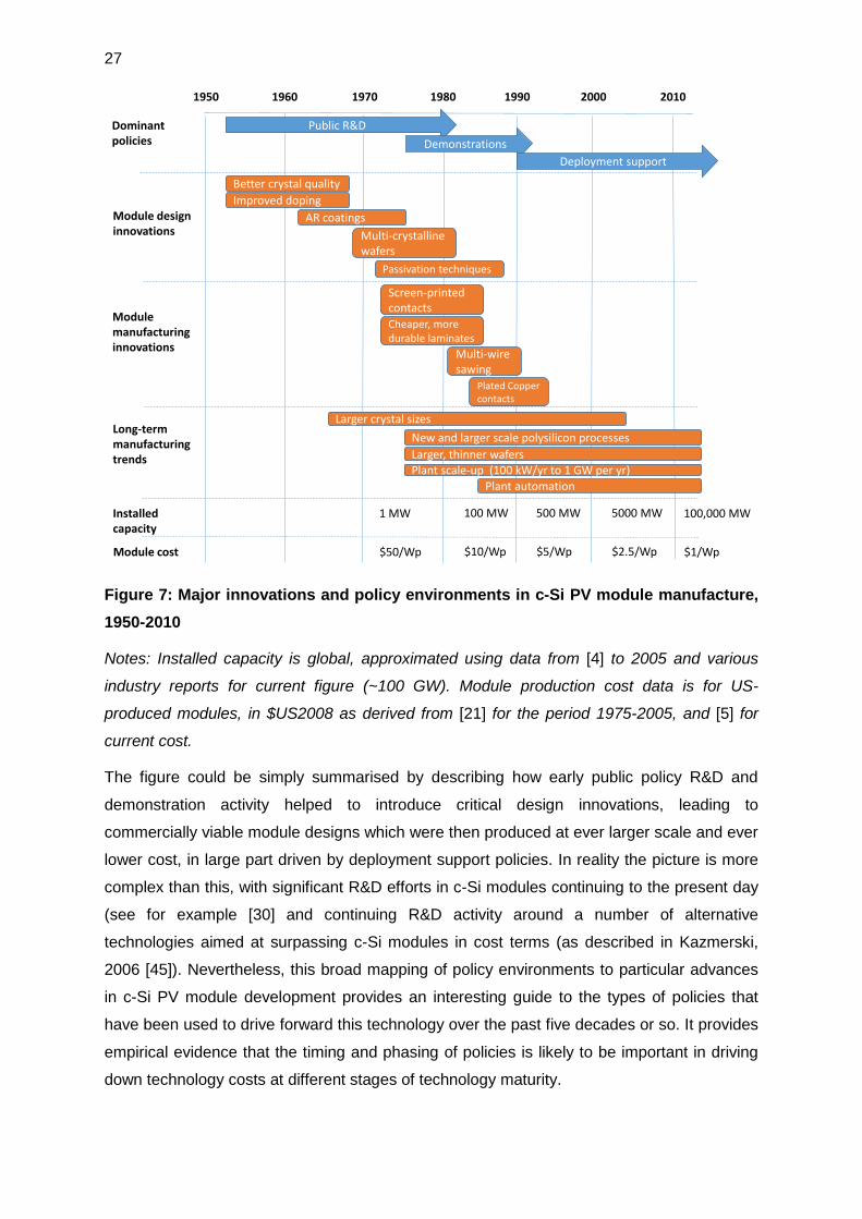
27
Figure 7: Major innovations and policy environments in c-Si PV module manufacture, 1950-2010
Notes: Installed capacity is global, approximated using data from [4] to 2005 and various
industry reports for current figure (~100 GW). Module production cost data is for US-
produced modules, in $US2008 as derived from [21] for the period 1975-2005, and [5] for
current cost.
The figure could be simply summarised by describing how early public policy R&D and
demonstration activity helped to introduce critical design innovations, leading to
commercially viable module designs which were then produced at ever larger scale and ever
lower cost, in large part driven by deployment support policies. In reality the picture is more
complex than this, with significant R&D efforts in c-Si modules continuing to the present day
(see for example [30] and continuing R&D activity around a number of alternative
technologies aimed at surpassing c-Si modules in cost terms (as described in Kazmerski,
2006 [45]). Nevertheless, this broad mapping of policy environments to particular advances
in c-Si PV module development provides an interesting guide to the types of policies that
have been used to drive forward this technology over the past five decades or so. It provides
empirical evidence that the timing and phasing of policies is likely to be important in driving
down technology costs at different stages of technology maturity.
1950 1960 1970 1980 1990 2000 2010
Dominantpolicies
Module designinnovations
Installedcapacity
Modulemanufacturinginnovations
Public R&DDemonstrations
Deployment support
Better crystal quality
AR coatingsMulti-crystallinewafers
Improved doping
Screen-printed contacts
Passivation techniques
Multi-wire sawing
Cheaper, more durable laminates
Plant automation
1 MW 100 MW 500 MW 5000 MW 100,000 MW
New and larger scale polysilicon processesLarger, thinner wafers
Long-term manufacturingtrends
Larger crystal sizes
Plant scale-up (100 kW/yr to 1 GW per yr)
Module cost $50/Wp $10/Wp $5/Wp $2.5/Wp $1/Wp
Plated Copper contacts
28
5 Discussion
Crystalline silicon PV modules have experienced significant cost-reductions since the 5%
efficiency breakthrough in the mid-1950s. A technology costing over $100/Wp in the early to
mid-1970s has fallen in cost by two orders of magnitude to reach today’s sub-$1/Wp level.
Many statistical analyses have demonstrated a close fit of module price to cumulative
deployment, with an approximate 20% price reduction in modules for each doubling of
installed module capacity (measured in Wp). It is tempting to interpret the relative
consistency of the estimated learning curves as evidence for a stable, almost intrinsic
relationship between module deployment and price reductions. This might indicate that
further price reductions could follow from continued deployment, which in turn supports
policies to further expand demand at a time when PV is still in many regions more expensive
than higher carbon alternative technologies. However, there is a well-established critique of
the use of such single factor learning curves in determining on-going relationships between
technology costs and technology deployment levels ([27], [3], [46], [47], [48], [49], [50]).
Criticisms include the differing relationship between price and underlying technology cost
depending on market dynamics, the possible existence of floors below which technologies’
costs cannot fall, the question over causality between deployment and technology price or
cost, the importance of other factors such as R&D, scale economies and input prices in
driving technology cost developments, and the difficulty of separating exogenous technical
change from that induced by deployment or technology-specific R&D.
Some of these shortcomings have been demonstrated through comparison of the statistical
studies presented in this paper, with different periods exhibiting different learning rates,
different factors (including silicon prices, scale effects and R&D) explaining price reductions
over different periods, and large variations in the impact of different explanatory factors on
price reductions depending on the other factors considered. This variety of findings does not
offer any simple policy prescriptions in terms of setting out whether further price reductions
should be achieved at least-cost through continued or even increased deployment policies,
increased public funding of innovation activities, or other public activities such as
demonstration programmes for new designs and manufacturing processes.
It is therefore important to investigate what specific innovations and improvements in module
design and manufacturing process have led to particular cost reductions, and the extent to
which these advances have been driven or supported by policies. For c-Si PV modules,
there were specific periods of module design innovation, particularly in the mid-1970s to
mid-1980s, which established the essential elements of today’s commercially-deployed PV
modules. What followed was a period of PV system monitoring, demonstration and
eventually market expansion, with the refined PV modules being produced in ever-larger
29
scale factories, and with manufacturers achieving significant reductions in key material
inputs (such as polysilicon), incremental improvements in efficiency and (as exemplified by
Chinese firms’ entry into the PV module production business) massive scale of production to
achieve cost reductions which have confounded most expectations.
Technology life-cycle analysis [36] suggests that many competitors try to introduce a variety
of designs of a new technology in an initial “fluid” phase of invention and innovation, before a
“dominant design” takes hold, heralding a “transitional” phase where innovation shifts to
manufacturing and learning by doing in the use and refinement of the technology. It appears
that c-Si PV modules with the design features exhibited in the mid-1980s (including
antireflection coatings and etched wafer surfaces to aid light absorption, wafer surface
passivation to prevent electron/hole recombination, glass and fluoropolymer lamination to
achieve durability at low cost) emerged as a dominant product design, with a further ten-fold
reduction in production cost over the next 27 years (1985-2012) following from
manufacturing scale-up, incremental design improvements (such as even greater
efficiencies through improved passivation and metal contact designs) and cost reductions in
key inputs (especially polysilicon).
Detailed roadmaps (for example Goodrich et al, 2013[51]; ITRPV, 2014 [52]) now exist for
how c-Si PV modules can begin to approach the $0.5/Wp sustainable cost production figure
which could make them truly competitive even without subsidy. These innovations include
cheaper polysilicon production using an increased share of Fluidised Bed Reactor-produced
silicon, manufacture of higher quality wafers, replacement of silicon carbide cutting fluid and
steel wires by longer lifetime, less contaminating diamond-coated steel wires for sawing
wafers, producing even thinner wafers, replacement of silver electrodes with cheaper
copper, increases in efficiency through use of thinner contacts and better passivation, and
achieving scale and bulk discounts in manufacturing equipment and processes.
A key question is what policy support, if any, will drive this further cost reduction. Zheng and
Kammen (2014) highlight the importance of patenting in explaining recent dramatic
reductions in c-Si PV modules prices [30], but as Breyer et al (2010) show, most of the R&D
in PV now comes from private, rather than public, sources [24]. Whilst analyses such as
Bettencourt et al (2013) highlight the importance of both public R&D and market size in PV
module price reductions [39], it appears that a healthy PV market is necessary to ensure that
manufacturers continue to search for ways to cost-effectively manufacture at scale the
known cell designs demonstrated in the laboratory from the mid -1980s onwards, when cell
efficiencies of 25% were exceeded (in monocrystalline Si cells). Indeed this provides an
analogue to the silicon chip market, whose “Moore’s Law” of a regular doubling of memory
capacity or computational power has been achieved through continuing investment in chip
30
improvements by manufacturers, as a result of a growing market and growing revenue
projections [53].
As well as helping to consider how to further advance innovation in c-Si PV itself, the
experience of c-Si PV may prove instructive for emerging PV technologies. The dramatic
reductions in c-Si PV module cost which resulted from the period of publicly-funded R&D
and demonstration during the mid-1970s to mid-1980s period presents the possibility that a
similar push for next-generation technologies might result in the emergence of even lower-
cost PV modules. A number of previous initiatives aimed at developing inorganic thin-film
technologies such as amorphous silicon (a-Si) and cadmium telluride (CdTe) have already
tried and failed to achieve the goal of toppling c-Si PV (see for example Braun and Skinner’s
(2007) account of BP Solar’s attempt to commercialise these technologies [54]).
Nevertheless, analysis suggests that “printable” PV (such as organic PV, perovskites, and
dye sensitised cells) presents the possibility of very low-cost PV modules [55], [56], [57],
should numerous shortcomings around stability, efficiency and in some cases material
toxicity be overcome. It may be that these challenges are best addressed through ambitious
programmes such as the US Flat-Plate Solar Array programme, which included targeted
initiatives to overcome multiple shortcomings in c-Si module design. Such programmes are
likely to require a strong “interface” function between module designers and users to ensure
that R&D and module field-testing and deployment activities interact with each-other [58].
Finally, the c-Si PV development story presents an important challenge for other forms of
low-carbon energy, particularly those which are less mature and where analysis suggests
that R&D has a very important role to play in cost reductions [59]. Such a shift has arguably
happened for other low-carbon technologies as well, such as onshore wind power during the
California “wind rush” of the early 1980s, when US patenting in several competing wind
turbine designs died down as deployment support policies incentivised a significant
acceleration in the installation of a particular design (the vertical, three-bladed, horizontal
axis, upwind turbine) which proved optimal in terms of performance and cost [60]. The
challenge for policy makers will be to understand when a dominant design has emerged,
such that focus can shift more firmly towards market creation policies in order to achieve
manufacturing scale-up and innovation to produce this “good-enough” version of the
technology.
31
6 Conclusions
This paper has reviewed the most important developments in c-Si PV module design and
manufacture since this technology was first commercially introduced in the 1950s, as well as
the major policies aimed at driving forward innovations and cost reductions. By mapping
periods of policy activity to innovations and cost reductions, as well as reviewing the
numerous quantitative analyses linking module prices to a range of factors, the paper offers
a perspective on how and why c-Si PV module prices have fallen over time.
Following c-Si modules’ early period of space cell development, the mid-1970s saw the
beginning of a dramatic period of innovation in module design and manufacture, in large part
driven by the US Jet Propulsion Laboratory’s Flat-Plate Solar Array project, which achieved
a more than five-fold reduction in module production costs and which helped establish
module designs not significantly different to those produced today. Following the emergence
of these module designs, increased demonstration and deployment support activities helped
to establish larger scale, more automated, lower cost manufacturing, helping to achieve the
current sub-$1/Wp production cost which has made many reconsider the economics of PV.
This picture of PV development contrasts with the relatively straightforward learning curve
analysis which (in its single-factor form) has equated a reasonably constant learning rate
with each doubling of cumulative installed capacity. It indicates that at relatively early stages
of technology development, intense and coordinated activity is required to achieve market-
ready designs. Subsequent deployment support is then necessary to stimulate further scale-
up and innovation in manufacturing, which could achieve equally if not more dramatic cost
reductions in the technology. The challenge remains to identify when such a dominant
design has emerged, in order that activity can shift from early design improvement to
manufacturing cost reductions.
Acknowledgements
This paper benefited greatly from detailed conversations with Nigel Mason of PV Consulting
Ltd and formerly of BP Solar, as well as input from Martin Green of UNSW, Jenny Nelson of
Imperial College London, and Chiara Candelise of Imperial College London and FEEM.
Opinions stated and any errors remain those of the authors alone.
.
32
References
[1] Fraunhofer Institute. Levelized Cost of Electricity, Renewable Energy Technologies
2013.
[2] Curtright AE, Morgan MG, Keith DW. Expert Assessments of Future Photovoltaic
Technologies. Environ Sci Technol 2008;42:9031–8.
[3] Nemet GF. Beyond the learning curve: factors influencing cost reductions in
photovoltaics. Energy Policy 2006;34:3218–32.
[4] Swanson RM. A vision for crystalline silicon photovoltaics. Prog Photovolt Res Appl
2006;14:443–53.
[5] Goodrich AC, Powell DM, James TL, Woodhouse M, Buonassisi T. Assessing the
drivers of regional trends in solar photovoltaic manufacturing. Energy Environ Sci
2013;6:2811.
[6] Bazilian M, Onyeji I, Liebreich M, MacGill I, Chase J, Shah J, et al. Re-considering
the economics of photovoltaic power. Renew Energy 2013;53:329–38.
[7] Ceccaroli B, Lohne O. Solar Grade Silicon Feedstock. Handb. Photovolt. Sci. Eng.
2nd Ed. 2nd ed., Wiley; 2010.
[8] Mason N. Personal communication with Ajay Gambhir 2014.
[9] Chapin DM, Fuller CS, Pearson GL. A New Silicon p‐n Junction Photocell for
Converting Solar Radiation into Electrical Power. J Appl Phys 1954;25:676–7.
[10] Perlin J. From Space to Earth: The Story of Solar Electricity. Earthscan; 1999.
[11] Rodriguez H, Guerrero I, Koch W, Endros AL, Franke D, Hassler C, et al. Bulk
Crystal Growth and Wafering for PV. Handb. Photovolt. Sci. Eng. 2nd Ed. 2nd ed., Wiley;
2010.
[12] Tobias I, del Canizo C, Alonso J. Crystalline Silicon Solar Cells and Modules.
Handb. Photovolt. Sci. Eng. 2nd Ed. 2nd ed., Wiley; 2010.
[13] Ghannam M, Sivoththaman S, Poortmans J, Szlufcik J, Nijs J, Mertens R, et al.
Trends in industrial silicon solar cell processes. Sol Energy 1997;59:101–10.
[14] PVInsights. PV Poly Silicon Weekly Spot Price. Pvinsights 2014.
[15] Green MA. The path to 25% silicon solar cell efficiency: History of silicon cell
evolution. Prog Photovolt Res Appl 2009;17:183–9.
[16] Wenham SR, Green MA. Silicon solar cells. Prog Photovolt Res Appl 1996;4:3–33.
33
[17] Green MA. Silicon photovoltaic modules: a brief history of the first 50 years. Prog
Photovolt Res Appl 2005;13:447–55.
[18] Hirshman WP, Knoll B. Annual Solar Module Survey. Photon Int 2014.
[19] Solar Plaza. Top 10 World’s Most Efficient Solar PV Modules (Mono-Crystalline)
2012.
[20] Christensen E. Flat-Plate Solar Array Project: 10 Years of Progress 1985.
[21] O’Connor AC, Loomis RJ, Braun FM. Retrospective Benefit-Cost Evaluation of DOE
Investment in Photovoltaic Energy Systems 2010.
[22] Byrne J, Kurdgelashvili L. The Role of Policy in PV Industry Growth; Past, Present
and Future. Handb. Photovolt. Sci. Eng. 2nd Ed. 2nd ed., Wiley; 2010.
[23] Solangi KH, Islam MR, Saidur R, Rahim NA, Fayaz H. A review on global solar
energy policy. Renew Sustain Energy Rev 2011;15:2149–63.
[24] Breyer C, Birkner C, Kersten F, Gerlach A, Goldschmidt JC, Stryi-Hipp G, et al.
Research and Development Investments in PV – a Limiting Factor for a Fast PV Diffusion?
6CV.5.22, Valencia, Spain: 2010.
[25] Grau T, Huo M, Neuhoff K. Survey of photovoltaic industry and policy in Germany
and China. Energy Policy 2012;51:20–37.
[26] Harmon C. Experience Curves of Photovoltaic Technology (Interim Report IR-00-
014) 2000.
[27] McDonald A, Schrattenholzer L. Learning rates for energy technologies. Energy
Policy 2001;29:255–61.
[28] Parente V, Goldemberg J, Zilles R. Comments on experience curves for PV
modules. Prog Photovolt Res Appl 2002;10:571–4.
[29] Van Sark WGJHM, Alsema EA, Junginger HM, de Moor HHC, Schaeffer GJ.
Accuracy of progress ratios determined from experience curves: the case of crystalline
silicon photovoltaic module technology development. Prog Photovolt Res Appl 2008;16:441–
53.
[30] Zheng C, Kammen DM. An innovation-focused roadmap for a sustainable global
photovoltaic industry. Energy Policy 2014;67:159–69.
[31] De La Tour A, Glachant M, Meniere Y. What cost for photovoltaic modules in 2020?
Lessons from experience curve models (Working Paper 13-ME-03) 2013.
34
[32] Miketa A, Schrattenholzer L. Experiments with a methodology to model the role of
R&D expenditures in energy technology learning processes; first results. Energy Policy
2004;32:1679–92.
[33] Kobos PH, Erickson JD, Drennen TE. Technological learning and renewable energy
costs: implications for US renewable energy policy. Energy Policy 2006;34:1645–58.
[34] Isoard S, Soria A. Technical change dynamics: evidence from the emerging
renewable energy technologies. Energy Econ 2001;23:619–36.
[35] Yu CF, van Sark WGJHM, Alsema EA. Unraveling the photovoltaic technology
learning curve by incorporation of input price changes and scale effects. Renew Sustain
Energy Rev 2011;15:324–37.
[36] Utterback JM. Mastering The Dynamics Of Innovation. Harvard Business Press;
1996.
[37] Peters M, Schneider M, Griesshaber T, Hoffmann VH. The impact of technology-
push and demand-pull policies on technical change – Does the locus of policies matter? Res
Policy 2012;41:1296–308.
[38] Huo M, Zhang X, He J. Causality relationship between the photovoltaic market and
its manufacturing in China, Germany, the US, and Japan. Front Energy 2011;5:43–8.
[39] Bettencourt LMA, Trancik JE, Kaur J. Determinants of the Pace of Global Innovation
in Energy Technologies. PLoS ONE 2013;8:e67864.
[40] Hoppmann J, Peters M, Schneider M, Hoffmann VH. The two faces of market
support—How deployment policies affect technological exploration and exploitation in the
solar photovoltaic industry. Res Policy 2013;42:989–1003.
[41] Watanabe C, Wakabayashi K, Miyazawa T. Industrial dynamism and the creation of
a “virtuous cycle” between R&D, market growth and price reduction: The case of
photovoltaic power generation (PV) development in Japan. Technovation 2000;20:299–312.
[42] Brown J, Hendry C. Public demonstration projects and field trials: Accelerating
commercialisation of sustainable technology in solar photovoltaics. Energy Policy
2009;37:2560–73.
[43] Jaeger-Waldau A. PV Status Report 2003: Research, Solar Cell Production and
Market Implementation in Japan, USA and the European Union 2003.
[44] Del Río P, Mir-Artigues P. Support for solar PV deployment in Spain: Some policy
lessons. Renew Sustain Energy Rev 2012;16:5557–66.
[45] Kazmerski LL. Solar photovoltaics R&D at the tipping point: A 2005 technology
overview. J Electron Spectrosc Relat Phenom 2006;150:105–35.
35
[46] Yeh S, Rubin E, Hounshell DA, Taylor MR. Uncertainties in Technology Experience
Curves for Integrated Assessment Models. Environ Sci Technol 2007;43:6907–14.
[47] Kahouli-Brahmi S. Technological learning in energy–environment–economy
modelling: A survey. Energy Policy 2008;36:138–62.
[48] Neij L. Cost development of future technologies for power generation—A study
based on experience curves and complementary bottom-up assessments. Energy Policy
2008;36:2200–11.
[49] Candelise C, Winskel M, Gross R. The dynamics of solar PV costs and prices as a
challenge for technology forecasting (forthcoming) 2013.
[50] Nordhaus WD. The Perils of the Learning Model for Modeling Endogenous
Technological Change. Energy J 2014;35.
[51] Goodrich A, Hacke P, Wang Q, Sopori B, Margolis R, James TL, et al. A wafer-
based monocrystalline silicon photovoltaics road map: Utilizing known technology
improvement opportunities for further reductions in manufacturing costs. Sol Energy Mater
Sol Cells 2013;114:110–35.
[52] ITRPV. International Technology Roadmap for Photovoltaic (2013 results) 2014.
[53] Mack CA. Fifty Years of Moore’s Law. IEEE Trans Semicond Manuf 2011;24:202–7.
[54] Braun GW, Skinner DE. Experience Scaling-Up Manufacturing of Emerging
Photovoltaic Technologies 2007.
[55] Azzopardi B, Emmott CJM, Urbina A, Krebs FC, Mutale J, Nelson J. Economic
assessment of solar electricity production from organic-based photovoltaic modules in a
domestic environment. Energy Environ Sci 2011;4:3741.
[56] Snaith HJ. Perovskites: The Emergence of a New Era for Low-Cost, High-Efficiency
Solar Cells. J Phys Chem Lett 2013;4:3623–30.
[57] Mulligan CJ, Wilson M, Bryant G, Vaughan B, Zhou X, Belcher WJ, et al. A
projection of commercial-scale organic photovoltaic module costs. Sol Energy Mater Sol
Cells 2014;120, Part A:9–17.
[58] Taylor M. Beyond technology-push and demand-pull: Lessons from California’s solar
policy. Energy Econ 2008;30:2829–54.
[59] Jamasb T. Technical Change Theory and Learning Curves: Patterns of Progress in
Electricity Generation Technologies. Energy J 2007;28.
[60] Nemet GF. Demand-pull, technology-push, and government-led incentives for non-
incremental technical change. Res Policy 2009;38:700–9.