Embed Size (px)
Citation preview
THE INSTITUTE OF SPACE AND ASTRONAUTICAL SCIENCE
YOSHINODAJ, SAGAMIHARA, KANAGAWA 229
ISAS RESEARCH NOTE
ISAS RN 636
Direct Measurements at the Sub-pixel Level of the X-ray Detection Efficiency of the CCD
on board the ASCA satellite
K. Yoshita1 , H. Tsunemi1,2,3, K. C. Gendreau4 , G. Penningto1l4
and M. \N. Bautz5
1anuary. 1998
I Osaka Univer ity, Machikaneyama, Toyonaka, Osaka, 560, Japan, 2CREST, Japan Science and Technology Corporation (JST),
3Visit,ing Professor, The Institute of Space and Astronautical Science Yoshinodai, Sagamihara, Kanagawa, 229, Japan,
4. TASA/GSFC and University of Mar Iland • N~ ....\ pI 5Massachusetts Institute of Technology (Y\ \......
To appear in IEEE Trans. tlcl. Sci., 45, in press, 1998
Direct Measurements at the Sub-pixel Level of the X-ray Detection Efficiency of the CCD on board the ASCA satellite
K. Yoshita1, H. Tsunemi1 ,2, K. C. Gendreau3 , G. Pennington3 and M. W. Bautz4
1 Osaka University, Machikaneyama, Toyonaka, 560 Japan 2 CREST, Japan Science and Technology Corporation (JST)
3 NASA/GSFC and University of Maryland 4 Massachusetts Institute of Technology
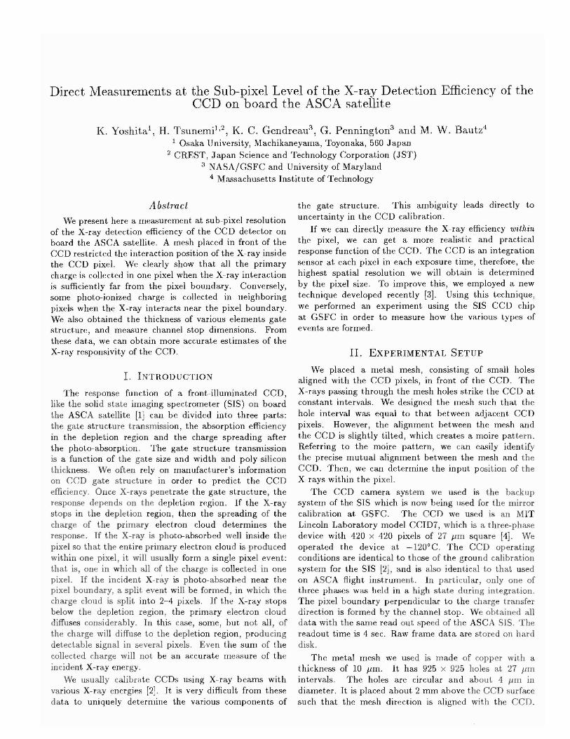
Abstract
We present here a measurement at sub-pixel resolution of the X-ray detection efficiency of the CCD detector on board the ASCA satellite. A mesh placed in front of the CCD restricted the interaction position of the X-ray inside the CCD pixel. We clearly show that all the primary charge is collected in one pixel when the X-ray interaction is sufficiently far from the pixel boundary. Conversely, some photo-ionized charge is collected in neighboring pixels when the X-ray interacts near the pixel boundary. We also obtained the thickness of various elements gate structure, and measure channel stop dimensions. From these data, we can obtain more accurate estimates of the X-ray responsivity of the CCD.
I. INTRODUCTION
The response function of a front-illuminated CCD, like the solid state imaging spectrometer (SIS) on board the ASCA satellite [1] can be divided into three parts: the gate structure transmission, the absorption efficiency in the depletion region and the charge spreading after the photo-absorption. The gate structure transmission is a function of the gate size and width and poly-silicon thickness. We often rely on manufacturer's information on CCD gate structure in order to predict the CCD efficiency. Once X-rays penetrate the gate structure, the response depends on the depletion region. If the X-ray stops in the depletion region, then the spreading of the charge of the primary electron cloud determines the response. If the X-ray is photo-absorbed well inside the pixel so that the entire primary electron cloud is produced within one pixel, it will usually form a single pixel event: that is, one in which all of the charge is collected in one pixel. If the incident X-ray is photo-absorbed near the pixel boundary, a split event will be formed, in which the charge cloud is split into 2-4 pixels. If the X-ray stops below the depletion region, the primary electron cloud diffuses considerably. In this case, some, but not all, of the charge will diffuse to the depletion region, producing detectable signal in several pixels. Even the sum of the collected charge will not be an accurate measure of the incident X-ray energy.
We usually calibrate CCDs using X-ray beams with various X-ray energies [2]. It is very difficult from these data to uniquely determine the various components of
the gate structure. This ambiguity leads directly to uncertainty in the CCD calibration.
If we can directly measure the X-ray efficiency within the pixel, we can get a more realistic and practical response function of the CCD. The CCD is an integration sensor at each pixel in each exposure time, therefore, the highest spatial resolution we will obtain is determined by the pixel size. To improve this, we employed a new technique developed recently [3]. Using this technique, we performed an experiment using the SIS CCD chip at GSFC in order to measure how the various types of events are formed.
II. EXPERIMENTAL SETUP
We placed a metal mesh, consisting of small holes aligned with the CCD pixels, in front of the CCD. The X-rays passing through the mesh holes strike the CCD at constant intervals. We designed the mesh such that the hole interval was equal to that between adjacent CCD pixels. However, the alignment between the mesh and the CCD is slightly tilted, which creates a moire pattern. Referring to the moire pattern, we can easily identify the precise mutual alignment between the mesh and the CCD. Then, we can determine the input position of the X-rays within the pixel.
The CCD camera system we used is the backup system of the SIS which is now being used for the mirror calibration at GSFC. The CCD we used is an MIT Lincoln Laboratory model CCID7, which is a three-phase device with 420 x 420 pixels of 27 J-Im square [4]. We operated the device at -120°C. The CCD operating conditions are identical to those of the ground calibration system for the SIS [2], and is also identical to that used on ASCA flight instrument. In particular, only one of three phases was held in a high state during integration. The pixel boundary perpendicular to the charge transfer direction is formed by the channel stop. We obtained all data with the same read out speed of the ASCA SIS. The readout time is 4 sec. Raw frame data are stored on hard disk.
The metal mesh we used is made of copper with a thickness of 10 J-Im. It has 925 x 925 holes at 27 J-Im intervals. The holes are circular and about 4 J-Im in diameter. It is placed about 2 mm above the CCD surface such that the mesh direction is aligned with the CCD.
.. 0...
..... § 0 0 u 0
0 I'l ... 0... 0
.<: ~
Y-L
Cu-Ka .j.
0 0...
0 4 6 6 10 Energy(keV)
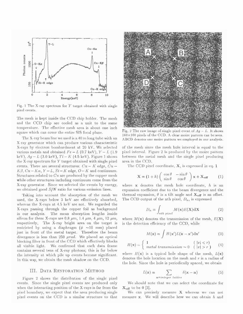
Fig. 1 The X-ray spectrum for Y target obtained with single pixel events.
The mesh is kept inside the CCD chip holder. The mesh and the CCD chip are cooled as a unit to the same temperature. The effective mesh area is about one inch square which can cover the entire SIS focal plane.
The X-ray beam line we used is a 40 m long tube with an X-ray generator which can produce various characteristic X-rays by electron bombardment at 20 kY. We selected various metals and obtained Fe - L (0.7 keY), Y - L (1.9 keV), Ag - L (3.0 keY), Ti - K (4.5 keY). Figure 1 shows the X-ray spectrum for Y target obtained with single pixel events. There are several structures: Cu - f{ edge, Cu 1(,8, Cu - J( 0', Y - L, Si - Kedge, 0 - I( and continuum. Structures related to Cu are produced by the copper mesh while other structures including continuum come from the X-ray generator. Since we selected the events by energy, we obtained good S/ N ratio for various emission lines.
Taking into account the absorption of the mesh we used, the X-rays below 3 keY are effectively absorbed, whereas the X-rays at 4.5 keY are not. We regarded the X-rays passing through the copper foil as background in our analysis. The mean absorption lengths inside silicon for these X-rays are 0.8 J1m, 1.4 J1m, 4 J1m, 12 J1m, respectively.. The X-ray bright area on the target is restricted by using a diaphragm (¢ ~10 mm) placed just in front of the metal target. Therefore the beam divergence is less than 250 J1rad. We placed an optical blocking filter in front of the CCD which effectively blocks all visible light. We confirmed that each data frame contains several tens of X-ray photons; this is far below the intensity at which pile up events become significant. In this way, we obtain the mesh shadow on the CCD.
III. DATA RESTORATION METHOD
Figure 2 shows the distribution of the single pixel events. Since the single pixel events are produced only when the interacting position of the X-rays is far from the pixel boundary, we expect that the area producing single pixel events on the CCD is a similar structur~ to that
2
Fig. 2 The raw image of single pixel event of Ag - L. It shows 160 x 160 pixels of the CCD. A clear moire pattern can be seen. ABCD denotes one moire pattern we employed in our analysis.
of the mesh since the mesh hole interval is equal to the pixel interval. Figure 2 is produced by the moire pattern between the metal mesh and the single pixel producing area in the CCD.
The CCD pixel coordinate, X, is expressed· in eq. 1
X = (1 + h) ( c?S ()() - sin()() ) x + Xoff (1)Sill cos
where x denotes the mesh hole coordinate, h is an expansion coefficient due to the beam divergence and the thermal expansion, () is a tilt angle and Xoff is an offset. The CCD output of the nth pixel, Do, is expressed
Do = ( M(x)E(X)dX (2) loth pixel
where M(x) denotes the transmission of the mesh, E(X) is the detection efficiency of the CCD, while
M(x) = JH(x')L(x - x')dx' (3)
1 ( Ixl < 7')H(x) = { (4)
metal lr'ansmission ~ 0 (Ixl > r )
where H(x) is a typical hole shape of the mesh, L(x) denotes the hole location on the mesh and 7' is a radius of the hole. Since the hole is periodically spaced, we obtain
L(x) = 8(x - n) (5) n=integer lattice
We should note that we can select the coordinate for X off to be 0 [3].
We can precisely measure X whereas we can not me~ure x. We will describe how we can obtain hand
() from the image. Figure 2 shows a grid pattern; le~ ABCD represent one element of that grid. Let AB be represented by X on the CCD coordinate and by x on the mesh coordinate, respectively. Then we obtain (1 + h)2 (X 2 + y2)/(x2 + y2) and tan() = (Yx - Xy)/(Xx + yy). Since AS denotes one element of the moire pattern, we can expect the following to hold:
In total, given the assumptions h, () ~ 0, which are true in our experiment, there are four possibilities. These are:
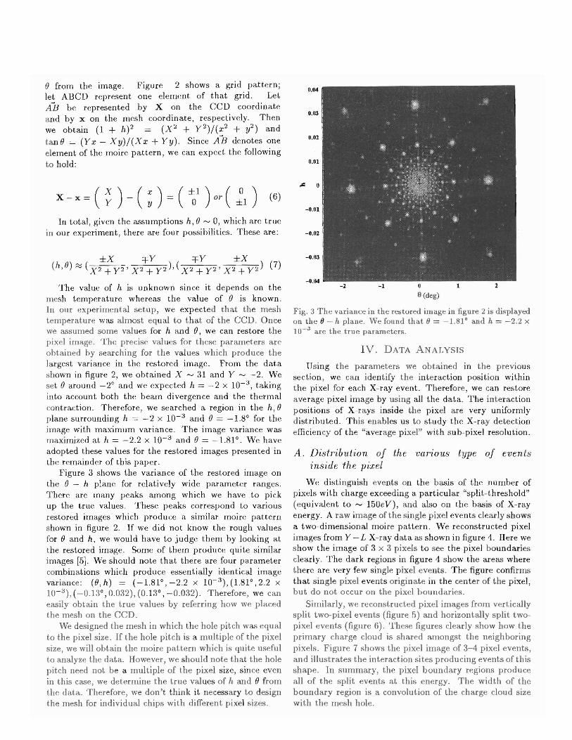
The value of h is unknown since it depends on the mesh temperature whereas the value of () is known. In our experimental setup, we expected that the mesh temperature was almost equal to that of the CCD. Once we assumed some values for hand (), we can restore the pixel image. The precise values for these parameters are obtained by searching for the values which produce the largest variance in the restored image. From the data shown in figure 2, we obtained X ~ 81 and Y ~ -2. We set () around _2° and we expected h = -2 X 10⁻³ , taking into account both the beam divergence and the thermal contraction. Therefore, we searched a region in the h, f) plane surrounding h = - 2 X 10⁻³ and () = -1.8° for the image with maximum variance. The image variance was maximized at h = -2.2 X 10⁻³ and () = -1.81°. We have adopted these values for the restored images presented in the remainder of this paper.
Figure 8 shows the variance of the restored image on the () - h plane for relatively wide parameter ranges. There are many peaks among which we have to pick up the true values. These peaks correspond to various restored images which produce a similar moire pattern shown in figure 2. If we did not know the rough values for () and h, we would have to judge them by looking at the restored image. Some of them produce quite similar images [5]. We should note that there are four parameter combinations which produce essentially identical image variance: «(),h) = (-1.81°,-2.2 x 10- 3 ),(1.81°,2.2 x 10-3 ), (-0.18°,0.032), (0.18°, -0.082). Therefore, we can easily obtain the true values by referring how we placed the mesh on the CCD.
We designed the mesh in which the hole pitch was equal to the pixel size. If the hole pitch is a multiple of the pixel size, we will obtain the moire pattern which is quite useful to analyze the data. However, we should note that the hole pitch need not be a multiple of the pixel size, since even in this case, we determine the true values of hand () from the data. Therefore, we don't think it necessary to design the mesh for individual chips with different pixel sizes.
0.04
0.03
0.02
0.01
..:=
-0.01
-0.02
-0.03
-0.04 -2 -1 0 2
9 (deg)
Fig. 3 The variance in the restored image in figure 2 is displayed on the 0 - h plane. We found that 0 = -1.81 0 and h = -2.2 X
10-3 are the trne parameters.
IV. DATA ANALYSIS
Using the parameters we obtained in the previous section, we can identify the interaction position within the pixel for each X-ray event. Therefore, we can restore average pixel image by using all the data. The interaction positions of X-rays inside the pixel are very uniformly distributed. This enables us to study the X-ray detection efficiency of the "average pixel" with sub-pixel resolution.
A. Distr'ibution of the various type of events inside the pixel
We distinguish events on the basis of the number of pixels with charge exceeding a particular "split-threshold" (equivalent to ~ 150eV), and also on the basis of X-ray energy. A raw image of the single pixel events clearly shows a two-dimensional moire pattern. We reconstructed pixel images from Y -L X-ray data as shown in figure 4. Here we show the image of 3 x 3 pixels to see the pixel boundaries clearly. The dark regions in figure 4 show the areas where there are very few single pixel events. The figure confirms that single pixel events originate in the center of the pixel, but do not occur on the pixel boundaries.
Similarly, we reconstructed pixel images from vertically split two-pixel events (figure 5) and horizontally split twopixel events (figure 6). These figures clearly show how the primary charge cloud is shared amongst the neighboring pixels. Figure 7 shows the pixel image of 3-4 pixel events, and illustrates the interaction sites producing events of this shape. In summary, the pixel boundary regions produce all of the split events at this energy. The width of the boundary region is a convolution of the charge cloud size with the mesh hole.
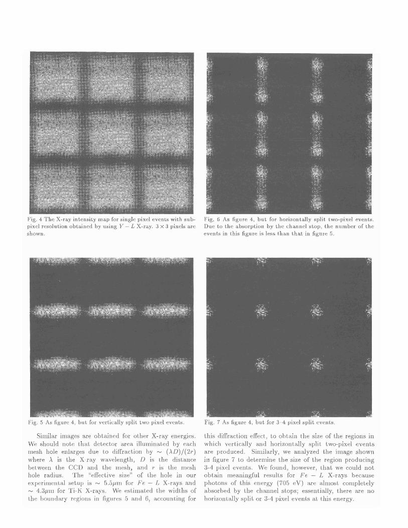
Fig. 4 The X-ray intensity map for single pixel events with subpixel resolution obtained by using Y - LX-ray. 3 x 3 pixels are shown.
Fig..5 As figure 4, but for vertically split two pixel events.
Similar images are obtained for other X-ray energies. We should note that detector area illuminated by each mesh hole enlarges due to diffraction by ~ (>.D)/(2r) where >. is the X-ray wavelength, D is the distance between the CCD and the mesh, and r is the mesh hole radius. The "effective size" of the hole in our experimental setup is ~ 5.5/lm for Fe - L X-rays and ~ 4.3/l111 for Ti-K X-rays. We estimated the widths of the boundary regions in figures 5 and 6, accounting for
Fig. 6 As figure 4, but for horizontally split two-pixel events. Due to the absorption by the channel stop, the number of the events in this figure is less than that in figure 5.
Fig. 7 As figure 4, but for 3-4 pixel split events.
this diffraction effect, to ohtain the size of tIle regions in which vertically and horizontally split two-pixel events are produced. Similarly, we analyzed the image shown in figure 7 to determine the size of the region producing 3-4 pixel events. We found, however, that we could not obtain meaningful results for Fe - L X-rays because photons of this energy (705 eV) are almost completely absorbed by the channel stops; essentially, there are no horizontally split or 3-4 pixel events at this energy.
o .... Ag-L Ti-K
* t • Horizontally split 2-pixel event
o Vertically split 2-pixel event l' Fe-L
o Height of 3-4 split event
• Width of 3-4 split event
5 10 Mean absorption length in Si v.m)
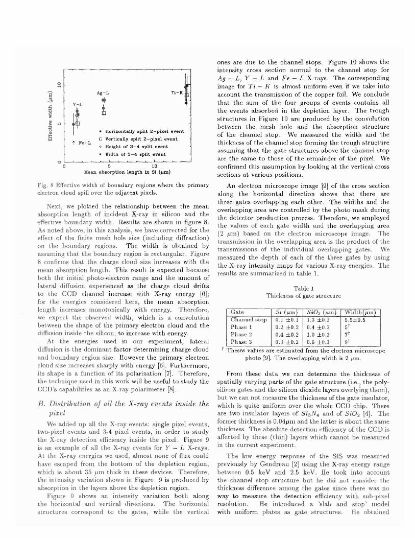
Fig. 8 Effective width of boundary regions where the primary electron cloud spill over the adjacent pixels.
Next, we plotted the relationship between the mean absorption length of incident X-ray in silicon and the effective boundary width. Results are shown in figure 8. As noted above, in this analysis, we have corrected for the effect of the finite mesh hole size (including diffraction) on the boundary regions. The width is obtained by assuming that the boundary region is rectangular. Figure 8 confirms that the charge cloud size increases with the mean absorption length. This result is expected because both the initial photo-electron range and the amount of lateral diffusion experienced as the charge cloud drifts to the CCD channel increase with X-ray energy [6]; for the energies considered here, the mean absorption length increases monotonically with energy. Therefore, we expect the observed width, which is a convolution between the shape of the primary electron cloud and the diffusion inside the silicon, to increase with energy.
At the energies llsed in our experiment, lateral diffusion is the dominant factor determining charge cloud and boundary region size. However the primary electron cloud size increases sharply with energy [6]. Furthermore, its shape is a function of its polarization [7]. Therefore, the technique used in this work will be useful to study the CCD's capabilities as an X-ray polarimeter [8].
B. Distribution of all the X-ray events inside the pixel
We added up all the X-ray events: single pixel events, two-pixel events and 3-4 pixel events, in order to study the X-ray detection efficiency inside the pixel. Figure 9 is an example of all the X-ray events for Y - LX-rays. At the X-ray energies we used, almost none of flux could have escaped from the bottom of the depletion region, which is about 35 Jjm thick in these devices. Therefore, the intensity variation shown in Figure 9 is produced by absorption in the layers above the depletion region.
Figure 9 shows an intensity variation both along the horizontal and vertical directions. The horizontal structures correspond to the gates, while the vertical
ones are due to the channel stops. Figure 10 shows the intensity cross section normal to the channel stop for Ag - L, Y - L and Fe - L X-rays. The corresponding image for Ti - K is almost uniform even if we take into account the transmission of the copper foil. We conclude that the sum of the four groups of events contains all the events absorbed in the depletion layer. The trough structures in Figure 10 are produced by the convolution between the mesh hole and the absorption structure of the channel stop. We mea.'mred the width and the thickness of the channel stop forming the trough structure assuming that the gate structures above the channel stop are the same to those of the remainder of the pixel. We confirmed this assumption by looking at the vertical cross sections at various positions.
An electron microscope image [9] of the cross section along the horizontal direction shows that there are three gates overlapping each other. The widths and the overlapping area are controlled by the photo-mask during the detector production process. Therefore, we employed the values of each gate width and the overlapping area (2 j-lm) based on the electron microscope image. The transmission in the overlapping area is the product of the transmissions of the individual overlapping gates. We measured the depth of each of the three gates by using the X-ray intensity maps for various X-ray energies. The results are summarized in table 1.
Table 1 Thickness of gate structure
Gate Si (/Lm) Si02 (/-&m) Width(/Lm) Channel stop 0.1 ±0.1 1.3 ±0.2 5.5±0.5 Phase 1 0.2 ±0.2 0.4 ±0.2 5' Phase 2 0.4 ±0.2 1.0 ±0.3 7' Phase 3 0.3 ±0.2 0.6 ±0.3 9'
t Theses values are estimated from the electron microscope photo [9]. The overlapping width is 2 /LID.
From these data we can determine the thickness of spatially varying parts of the gate structure (i.e., the polysilicon gates and the silicon dioxide layers overlying them), but we can not measure the thickness of the gate insulator, which is quite uniform over the whole CCD chip. There are two insulator layers of Si3 N4 and of Si02 [4]. The former thickness is 0.04j-lm and the latter is about the same thickness. The absolute detection efficiency of the CCD is affected by these (thin) layers which cannot be measured in the current experiment.
The low energy response of the SIS was measured previously by Gendreau [2] using the X-ray energy range between 0.5 keY and 2.5 keY. He took into account the channel stop structure but he did not consider the thickness difference among the gates since there was no way to measure the detection efficiency with sub-pixel resolution. He introduced a 'slab and stop' model with uniform plates as gate structures. He obtained
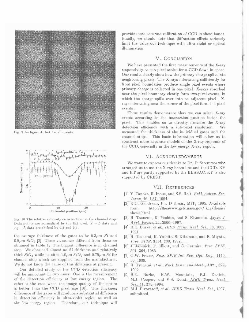
Fig. 9 As figure 4, but for all events.
~r-~~-~~--,--~~~~-.---,.-~--r-, ...
o 10 20 Horizontal position (}<m)
Fig. 10 The relative intensity cross section on the channel stop. Data points are normalized by the flat level. Y - L data and Ag - L data are shifted by 0.2 and 0.4.
the average thickness of the gates to be 0.3{lm Si and 0.5{lIn SiOz [2]. These values are different from those we obtained in table 1. The biggest difference is in channel stop. We obtained almost no Si thickness and relatively thick SiOz while he cited l.O{lm SiOz and 0.75{lm Si for channel stop which are supplied from the manufacturer. We do not know the cause of this difference at present.
Our detailed study of the CCD detection efficiency will be important in two cases. One is the measurement of the detection efficiency at low energy region. The other is the case when the image quality of the optics is better than the CCD pixel size [10]. The thickness difference of the gates will produce a substantial difference in detection efficiency in ultra-violet region as well as the low-energy region. Therefore, our technique will
provide more accurate calibration of CCD in those bands. Finally, we should note that diffraction effects seriously limit the value our technique with ultra-violet or optical illumination.
V. CONCLUSION
We have presented the first measurements of the X-ray responsivity at sub-pixel scales for a CCD flown in space. Our results clearly show how the primary charge splits into neighboring pixels. The X-rays interacting sufficiently far from pixel boundaries produce single pixel events whose primary charge is collected in one pixel. X-rays absorbed near the pixel boundary clearly form tw<rpixel events, in which the charge spills over into an adjacent pixel. Xrays interacting near the corner of the pixel form 3-4 pixel events.
These results demonstrate that we can select X-ray events according to the interaction position inside the pixel. This enables us to directly measure the X-ray detection efficiency with a sub-pixel resolution. We measured the thickness of the individual gates and the channel stops. This basic information will allow us to construct more accurate models of the X-ray response of the CCD, especially in the low energy X-ray region.
VI. ACKNOWLEDGMENTS
We want to express our thanks to Dr. P. Seremtsos who arranged us to use the X-ray beam line and the CCD. KY and HT are partly supported by the HEASAC. KY is also supported by CREST.
VII. REFERENCES
[1] Y. Tanaka, H. Inoue, and S.S. Holt, Publ. Astron. Soc. Japan, 46 L37, 1994.
[2f'"KG: Gendreau, Ph. D thesis, MIT, 1995. Available from http://lheawww .gsfc.nasa.gov/'Kcg/thesis/ thesis.html .
[3] H. Tsunemi, K. Yoshita, and S. Kitamoto, l2.pan J. A pl. P11'I "C, 36, 2906, 1997.
[4] B.E. Burke, et al., IEEE Trans. Nucl. Sci., 38, 1069, 1991.
[5] H. Tsunemi, K. Yoshita, S. Kitamoto, and E. Miyata, Proc. SPIE, 3114, 230, 1997.
[6] J. Janesick, T. Elliott, and G. Garmire, Proc. SPIE, 597,364, 1985.
[7] G.W. Fraser, Proc. SPIE Int. Soc. Opt. Eng., 1140, 50, 1989.
[8] H. Tsunemi, et al., Nucl. Instr. and Meth., A321, 629, 1992.
[9] B.E. Burke, R.W. Mountain, P.J. Daniels, M.J. Cooper, and V.S. Dolat IEEE Trans. Nucl. Sci., 41,375, 1994.
[10]~Pivovaroff, et al., IEEE Trans. Nucl. Sci., 1997, submitted.