Embed Size (px)
Citation preview
This document is downloaded from DR‑NTU (https://dr.ntu.edu.sg)Nanyang Technological University, Singapore.
The integration of InGaP LEDs with CMOS on 200mm silicon wafers
Wang, Bing; Lee, Kwang Hong; Wang, Cong; Wang, Yue; Made, Riko I.; Sasangka, WardhanaAji; Nguyen, Viet Cuong; Lee, Kenneth Eng Kian; Tan, Chuan Seng; Yoon, Soon Fatt;Fitzgerald, Eugene A.; Michel, Jurgen
2017
Wang, B., Lee, K. H., Wang, C., Wang, Y., Made, R. I., Sasangka, W. A., . . . Michel, J. (2017).The integration of InGaP LEDs with CMOS on 200 mm silicon wafers. Proceedings of SPIE ‑Smart Photonic and Optoelectronic Integrated Circuits XIX, 10107, 101070Y‑.doi:10.1117/12.2252030
https://hdl.handle.net/10356/105701
https://doi.org/10.1117/12.2252030
© 2017 SPIE. All rights reserved. This paper was published in Proceedings of SPIE ‑ SmartPhotonic and Optoelectronic Integrated Circuits XIX and is made available with permissionof SPIE.
Downloaded on 12 Mar 2022 19:15:35 SGT
The integration of InGaP LEDs with CMOS on 200 mm Silicon wafers
Bing Wang*a, Kwang Hong Leea, Cong Wanga,b, Yue Wanga, Riko I. Madea, Wardhana Aji Sasangkaa, Viet Cuong Nguyena, Kenneth Eng Kian Leea, Chuan Seng Tana,b, Soon Fatt Yoona,b,
Eugene A. Fitzgeralda,c, and Jurgen Michela,d
aLow Energy Electronic Systems IRG (LEES), Singapore-MIT Alliance for Research and Technology, 1 Create Way, Singapore 138602; bSchool of Electrical and Electronic Engineering, Nanyang Technological University, 50 Nanyang Avenue, Singapore 639798; cDept. of Materials Science and Engineering, Massachusetts Institute of Technology, 77 Mass. Ave., Cambridge, MA
02139, USA; dMicrophotonics Center, Massachusetts Institute of Technology, 77 Mass. Ave., Cambridge, MA 02139, USA
ABSTRACT
The integration of photonics and electronics on a converged silicon CMOS platform is a long pursuit goal for both academe and industry. We have been developing technologies that can integrate III-V compound semiconductors and CMOS circuits on 200 mm silicon wafers. As an example we present our work on the integration of InGaP light-emitting diodes (LEDs) with CMOS. The InGaP LEDs were epitaxially grown on high-quality GaAs and Ge buffers on 200 mm (100) silicon wafers in a MOCVD reactor. Strain engineering was applied to control the wafer bow that is induced by the mismatch of coefficients of thermal expansion between III-V films and silicon substrate. Wafer bonding was used to transfer the foundry-made silicon CMOS wafers to the InGaP LED wafers. Process trenches were opened on the CMOS layer to expose the underneath III-V device layers for LED processing. We show the issues encountered in the 200 mm processing and the methods we have been developing to overcome the problems.
Keywords: InGaP LED, CMOS integration, strain engineering, wafer bonding
1. INTRODUCTION The integration of III-V compound semiconductors with silicon CMOS circuits on a converged platform opens up new ways towards many advanced applications for photonics and electronics, e.g. photonic integrated circuits, advanced RF chips, optical interconnects, and so on. For such an integration platform the incorporation of III-V materials should follow a similar method of conventional CMOS process so that current CMOS facilities can be used, and high integration density and low cost can be achieved. In addition, the interconnections between III-V and CMOS should be done in close proximity, and any contaminations for the silicon CMOS should be avoided due to the incorporation of III-V materials. We are developing such a platform that can integrate various III-V compound semiconductors including III–As/P and GaN with silicon CMOS circuits [1]. We envision that applications of RF and optoelectronic would benefit from such integration. As an example, we report the integration of InGaP light-emitting diodes (LEDs) with silicon CMOS. InGaP red LEDs are commercially available for about two decades and the integration with CMOS was explored previously [2, 3]. Nowadays InGaP LEDs have various applications such as lighting, display, sensing, etc. The integration with CMOS control circuits would enable new functions and applications, for instance smart lighting and full-color micro-LED arrays. Another potential application is on-chip optical interconnects. Although it is usually recognized that lasers should be used to achieve high bandwidth data transfer, modeling work shows that in certain circumstances LEDs as light sources for on-chip optical interconnects in multicore processors may achieve low power consumption operation [4]. The realization of these applications relies on successful demonstration of integrated LED and CMOS chips. We report our integration scheme, the issues encountered in 200 mm wafer processing, and the methods we are developing to overcome the problems.
Smart Photonic and Optoelectronic Integrated Circuits XIX, edited by Louay A. Eldada, El-Hang Lee, Sailing He, Proc. of SPIE Vol. 10107, 101070Y · © 2017 SPIE
CCC code: 0277-786X/17/$18 · doi: 10.1117/12.2252030
Proc. of SPIE Vol. 10107 101070Y-1Downloaded From: https://www.spiedigitallibrary.org/conference-proceedings-of-spie on 05 Aug 2019Terms of Use: https://www.spiedigitallibrary.org/terms-of-use
Si CMOS Si CMOS
III -V buffer
Ge buffer
Si substrate
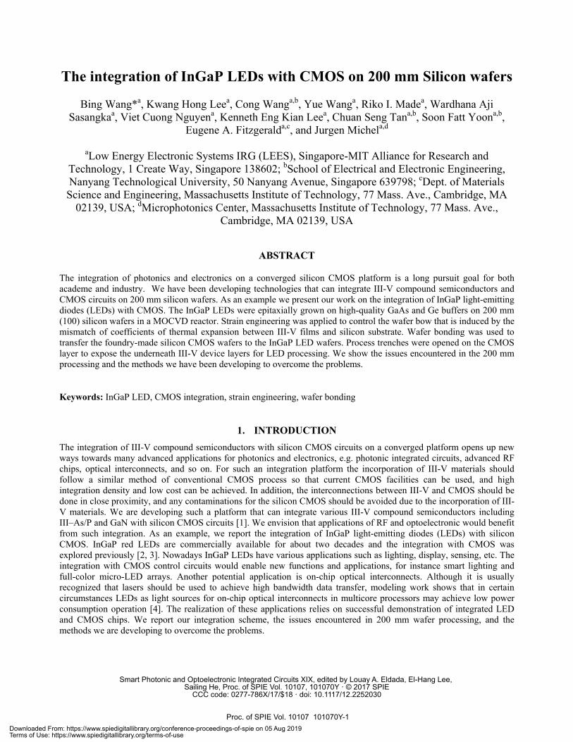
Our integration scheme is based on processing of the silicon CMOS wafers in a foundry while processing InGaP LED wafers separately. The CMOS circuit layer is then transferred to the LED wafer by a double wafer bonding process. Windows will be opened on CMOS layer to expose the underneath III-V layers. The LED processing is then done in the opened trenches. The interconnection between CMOS and LED is done afterwards in CMOS foundry. Figure 1 schematically shows an integrated InGaP LED + CMOS wafer. More detailed integration flow will be shown below.
Figure 1. Schematic drawing of integrated InGaP LED + CMOS wafer.
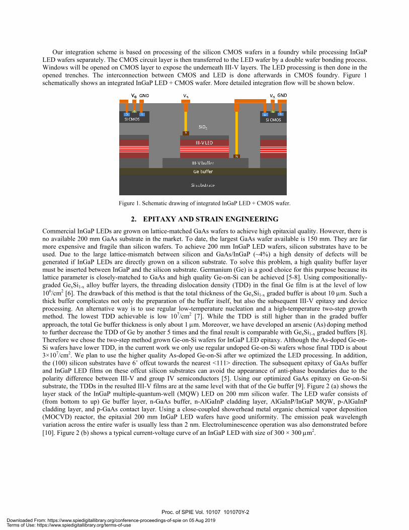
2. EPITAXY AND STRAIN ENGINEERING Commercial InGaP LEDs are grown on lattice-matched GaAs wafers to achieve high epitaxial quality. However, there is no available 200 mm GaAs substrate in the market. To date, the largest GaAs wafer available is 150 mm. They are far more expensive and fragile than silicon wafers. To achieve 200 mm InGaP LED wafers, silicon substrates have to be used. Due to the large lattice-mismatch between silicon and GaAs/InGaP (~4%) a high density of defects will be generated if InGaP LEDs are directly grown on a silicon substrate. To solve this problem, a high quality buffer layer must be inserted between InGaP and the silicon substrate. Germanium (Ge) is a good choice for this purpose because its lattice parameter is closely-matched to GaAs and high quality Ge-on-Si can be achieved [5-8]. Using compositionally-graded GexSi1-x alloy buffer layers, the threading dislocation density (TDD) in the final Ge film is at the level of low 106/cm2 [6]. The drawback of this method is that the total thickness of the GexSi1-x graded buffer is about 10 μm. Such a thick buffer complicates not only the preparation of the buffer itself, but also the subsequent III-V epitaxy and device processing. An alternative way is to use regular low-temperature nucleation and a high-temperature two-step growth method. The lowest TDD achievable is low 107/cm2 [7]. While the TDD is still higher than in the graded buffer approach, the total Ge buffer thickness is only about 1 μm. Moreover, we have developed an arsenic (As) doping method to further decrease the TDD of Ge by another 5 times and the final result is comparable with GexSi1-x graded buffers [8]. Therefore we chose the two-step method grown Ge-on-Si wafers for InGaP LED epitaxy. Although the As-doped Ge-on-Si wafers have lower TDD, in the current work we only use regular undoped Ge-on-Si wafers whose final TDD is about 3×10⁷/cm2. We plan to use the higher quality As-doped Ge-on-Si after we optimized the LED processing. In addition, the (100) silicon substrates have 6˚ offcut towards the nearest <111> direction. The subsequent epitaxy of GaAs buffer and InGaP LED films on these offcut silicon substrates can avoid the appearance of anti-phase boundaries due to the polarity difference between III-V and group IV semiconductors [5]. Using our optimized GaAs epitaxy on Ge-on-Si substrate, the TDDs in the resulted III-V films are at the same level with that of the Ge buffer [9]. Figure 2 (a) shows the layer stack of the InGaP multiple-quantum-well (MQW) LED on 200 mm silicon wafer. The LED wafer consists of (from bottom to up) Ge buffer layer, n-GaAs buffer, n-AlGaInP cladding layer, AlGaInP/InGaP MQW, p-AlGaInP cladding layer, and p-GaAs contact layer. Using a close-coupled showerhead metal organic chemical vapor deposition (MOCVD) reactor, the epitaxial 200 mm InGaP LED wafers have good uniformity. The emission peak wavelength variation across the entire wafer is usually less than 2 nm. Electroluminescence operation was also demonstrated before [10]. Figure 2 (b) shows a typical current-voltage curve of an InGaP LED with size of 300 × 300 μm2.
Proc. of SPIE Vol. 10107 101070Y-2Downloaded From: https://www.spiedigitallibrary.org/conference-proceedings-of-spie on 05 Aug 2019Terms of Use: https://www.spiedigitallibrary.org/terms-of-use
Voltage (V)
0.00 1
1
0.03 %
0.04 1
GDevice size: 0.3x0.3 mm'
/i1
aAs contact la er: 70nm C /Zn -do.ed
p- AIGaInP cladding layer: 300nm Zn -doped
AIGaInP undoped layer: 100nm
AIGaInP undoped layer: 50nm
n-AIGaInP cladding: 150nm
n-InAIP:
n -GaAs buffer: 200 nm
Ge buffer 0.711m
8" Si substrate
Figure 2. (a) Layer stack of an InGaP MQW LED on 200 mm (8 inch) silicon substrate. The InAlP, AlGaInP, and InGaP layers are lattice-matched to GaAs. (b) Current-voltage (I-V) curve of a 300 × 300 μm2 InGaP LED.
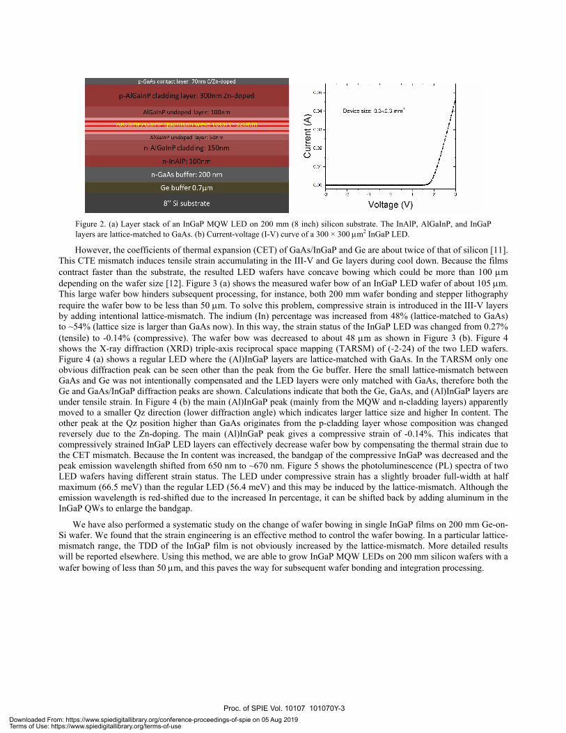
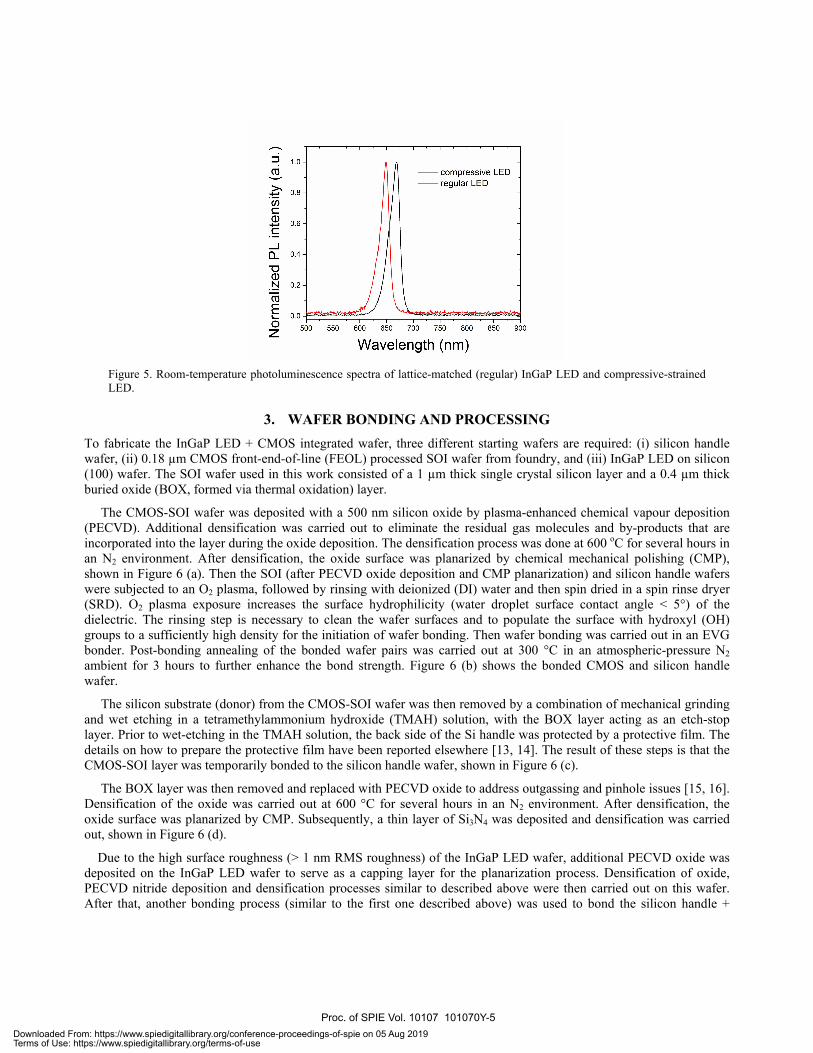
However, the coefficients of thermal expansion (CET) of GaAs/InGaP and Ge are about twice of that of silicon [11]. This CTE mismatch induces tensile strain accumulating in the III-V and Ge layers during cool down. Because the films contract faster than the substrate, the resulted LED wafers have concave bowing which could be more than 100 μm depending on the wafer size [12]. Figure 3 (a) shows the measured wafer bow of an InGaP LED wafer of about 105 μm. This large wafer bow hinders subsequent processing, for instance, both 200 mm wafer bonding and stepper lithography require the wafer bow to be less than 50 μm. To solve this problem, compressive strain is introduced in the III-V layers by adding intentional lattice-mismatch. The indium (In) percentage was increased from 48% (lattice-matched to GaAs) to ~54% (lattice size is larger than GaAs now). In this way, the strain status of the InGaP LED was changed from 0.27% (tensile) to -0.14% (compressive). The wafer bow was decreased to about 48 μm as shown in Figure 3 (b). Figure 4 shows the X-ray diffraction (XRD) triple-axis reciprocal space mapping (TARSM) of (-2-24) of the two LED wafers. Figure 4 (a) shows a regular LED where the (Al)InGaP layers are lattice-matched with GaAs. In the TARSM only one obvious diffraction peak can be seen other than the peak from the Ge buffer. Here the small lattice-mismatch between GaAs and Ge was not intentionally compensated and the LED layers were only matched with GaAs, therefore both the Ge and GaAs/InGaP diffraction peaks are shown. Calculations indicate that both the Ge, GaAs, and (Al)InGaP layers are under tensile strain. In Figure 4 (b) the main (Al)InGaP peak (mainly from the MQW and n-cladding layers) apparently moved to a smaller Qz direction (lower diffraction angle) which indicates larger lattice size and higher In content. The other peak at the Qz position higher than GaAs originates from the p-cladding layer whose composition was changed reversely due to the Zn-doping. The main (Al)InGaP peak gives a compressive strain of -0.14%. This indicates that compressively strained InGaP LED layers can effectively decrease wafer bow by compensating the thermal strain due to the CET mismatch. Because the In content was increased, the bandgap of the compressive InGaP was decreased and the peak emission wavelength shifted from 650 nm to ~670 nm. Figure 5 shows the photoluminescence (PL) spectra of two LED wafers having different strain status. The LED under compressive strain has a slightly broader full-width at half maximum (66.5 meV) than the regular LED (56.4 meV) and this may be induced by the lattice-mismatch. Although the emission wavelength is red-shifted due to the increased In percentage, it can be shifted back by adding aluminum in the InGaP QWs to enlarge the bandgap.
We have also performed a systematic study on the change of wafer bowing in single InGaP films on 200 mm Ge-on-Si wafer. We found that the strain engineering is an effective method to control the wafer bowing. In a particular lattice-mismatch range, the TDD of the InGaP film is not obviously increased by the lattice-mismatch. More detailed results will be reported elsewhere. Using this method, we are able to grow InGaP MQW LEDs on 200 mm silicon wafers with a wafer bowing of less than 50 μm, and this paves the way for subsequent wafer bonding and integration processing.
Proc. of SPIE Vol. 10107 101070Y-3Downloaded From: https://www.spiedigitallibrary.org/conference-proceedings-of-spie on 05 Aug 2019Terms of Use: https://www.spiedigitallibrary.org/terms-of-use

[001
] dire
ctio
n-.
1-.
1--
.1
61.."
'l6
is)
000)
N -
Is
7.56..7.54
C 7.52
-4.22 -4.2 -4.18 -4.16Qx (him) in [1 -1 0] direction
c7, 7.56E.,.. 7.54
C 7.52
-4.25 -4.2 -4.15Qx (/nm) in [1 -1 0] direction
[001
] dire
ctio
n--
.1-.
16
:`"A
6)6)
00a)
N
DEFLECTION MAP Di13d1 UNITS: µm
Scan CommentID: 908ag Diameter: 200
:45, R:O, M:1.0
STATISTICS:Film the -
verage: -26.44Minimum: -47.38Maximum: 0.00e +000
Std Dee: 12.58
DEFLECTION MAP UNITS: µm
Scan C'ornrnent:ID 907dkj Di meter: 200
:45, R:O, M:1.0
STATISTICS:Film the -
verage: -55.26Minimum: -105.40
Maximum: 3.77e -007
Std Dev 29.53
Figure 3. (a) Wafer bow of an InGaP LED that is lattice-matched with GaAs. The largest wafer bow is about 105 μm. (b) Wafer bow of a compressive-strained InGaP wafer, the largest wafer bow is about 48 μm.
(a) (b)
Figure 4. X-ray diffraction reciprocal space maps of a lattice-matched InGaP LED on Ge-on-Si (a), and a compressive strained InGaP LED on Ge-on-Si (b). The diffraction peaks of Ge, GaAs, and (Al)InGaP are indicated by arrows. Interference fringes are clearly seen in (b).
Proc. of SPIE Vol. 10107 101070Y-4Downloaded From: https://www.spiedigitallibrary.org/conference-proceedings-of-spie on 05 Aug 2019Terms of Use: https://www.spiedigitallibrary.org/terms-of-use
zWavelength (nm)
aN o2-
compressive LED
I I
regular LED
o0.0
I
Fnn FFn An FFn Inn ]Fn Ann Ac( Q(1f)
OA-
n
Figure 5. Room-temperature photoluminescence spectra of lattice-matched (regular) InGaP LED and compressive-strained LED.
3. WAFER BONDING AND PROCESSING To fabricate the InGaP LED + CMOS integrated wafer, three different starting wafers are required: (i) silicon handle wafer, (ii) 0.18 µm CMOS front-end-of-line (FEOL) processed SOI wafer from foundry, and (iii) InGaP LED on silicon (100) wafer. The SOI wafer used in this work consisted of a 1 µm thick single crystal silicon layer and a 0.4 µm thick buried oxide (BOX, formed via thermal oxidation) layer.
The CMOS-SOI wafer was deposited with a 500 nm silicon oxide by plasma-enhanced chemical vapour deposition (PECVD). Additional densification was carried out to eliminate the residual gas molecules and by-products that are incorporated into the layer during the oxide deposition. The densification process was done at 600 oC for several hours in an N2 environment. After densification, the oxide surface was planarized by chemical mechanical polishing (CMP), shown in Figure 6 (a). Then the SOI (after PECVD oxide deposition and CMP planarization) and silicon handle wafers were subjected to an O2 plasma, followed by rinsing with deionized (DI) water and then spin dried in a spin rinse dryer (SRD). O2 plasma exposure increases the surface hydrophilicity (water droplet surface contact angle < 5°) of the dielectric. The rinsing step is necessary to clean the wafer surfaces and to populate the surface with hydroxyl (OH) groups to a sufficiently high density for the initiation of wafer bonding. Then wafer bonding was carried out in an EVG bonder. Post-bonding annealing of the bonded wafer pairs was carried out at 300 °C in an atmospheric-pressure N2 ambient for 3 hours to further enhance the bond strength. Figure 6 (b) shows the bonded CMOS and silicon handle wafer.
The silicon substrate (donor) from the CMOS-SOI wafer was then removed by a combination of mechanical grinding and wet etching in a tetramethylammonium hydroxide (TMAH) solution, with the BOX layer acting as an etch-stop layer. Prior to wet-etching in the TMAH solution, the back side of the Si handle was protected by a protective film. The details on how to prepare the protective film have been reported elsewhere [13, 14]. The result of these steps is that the CMOS-SOI layer was temporarily bonded to the silicon handle wafer, shown in Figure 6 (c).
The BOX layer was then removed and replaced with PECVD oxide to address outgassing and pinhole issues [15, 16]. Densification of the oxide was carried out at 600 °C for several hours in an N2 environment. After densification, the oxide surface was planarized by CMP. Subsequently, a thin layer of Si3N4 was deposited and densification was carried out, shown in Figure 6 (d).
Due to the high surface roughness (> 1 nm RMS roughness) of the InGaP LED wafer, additional PECVD oxide was deposited on the InGaP LED wafer to serve as a capping layer for the planarization process. Densification of oxide, PECVD nitride deposition and densification processes similar to described above were then carried out on this wafer. After that, another bonding process (similar to the first one described above) was used to bond the silicon handle +
Proc. of SPIE Vol. 10107 101070Y-5Downloaded From: https://www.spiedigitallibrary.org/conference-proceedings-of-spie on 05 Aug 2019Terms of Use: https://www.spiedigitallibrary.org/terms-of-use
Si Handle Waf-
(a)
Si Handle removal
F'tCvD SiO2SiN
InGaP LED
Si (001) Wafer
(f)
Sí02 (BO
SOI-CM OS
(Donor)
(b)
2nd Bonding
bBottom Si substrate
removal
Si Handle Wafer
(c)
irBOX removal and PECVD
Si02 + SiN deposition
Si Handle Wafe
InGaP LED
Si (001) Wafer
(e)
110(d)
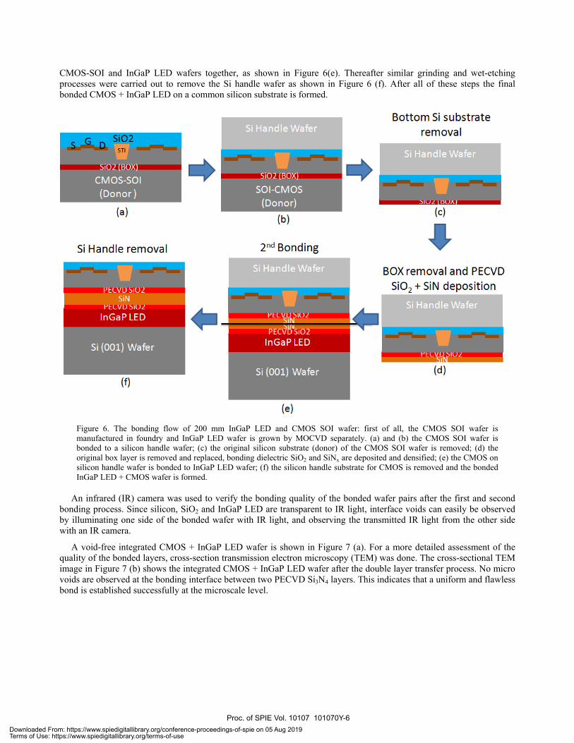
CMOS-SOI and InGaP LED wafers together, as shown in Figure 6(e). Thereafter similar grinding and wet-etching processes were carried out to remove the Si handle wafer as shown in Figure 6 (f). After all of these steps the final bonded CMOS + InGaP LED on a common silicon substrate is formed.
Figure 6. The bonding flow of 200 mm InGaP LED and CMOS SOI wafer: first of all, the CMOS SOI wafer is manufactured in foundry and InGaP LED wafer is grown by MOCVD separately. (a) and (b) the CMOS SOI wafer is bonded to a silicon handle wafer; (c) the original silicon substrate (donor) of the CMOS SOI wafer is removed; (d) the original box layer is removed and replaced, bonding dielectric SiO2 and SiNx are deposited and densified; (e) the CMOS on silicon handle wafer is bonded to InGaP LED wafer; (f) the silicon handle substrate for CMOS is removed and the bonded InGaP LED + CMOS wafer is formed.
An infrared (IR) camera was used to verify the bonding quality of the bonded wafer pairs after the first and second bonding process. Since silicon, SiO2 and InGaP LED are transparent to IR light, interface voids can easily be observed by illuminating one side of the bonded wafer with IR light, and observing the transmitted IR light from the other side with an IR camera.
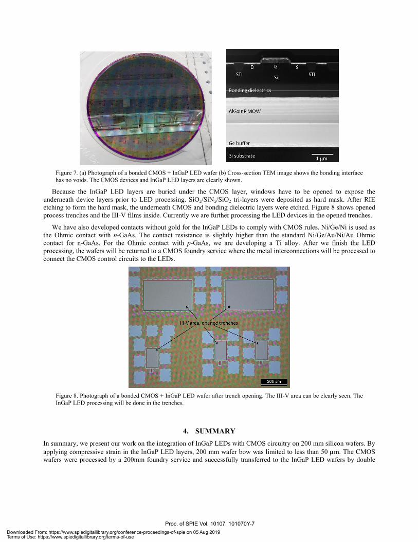
A void-free integrated CMOS + InGaP LED wafer is shown in Figure 7 (a). For a more detailed assessment of the quality of the bonded layers, cross-section transmission electron microscopy (TEM) was done. The cross-sectional TEM image in Figure 7 (b) shows the integrated CMOS + InGaP LED wafer after the double layer transfer process. No micro voids are observed at the bonding interface between two PECVD Si3N4 layers. This indicates that a uniform and flawless bond is established successfully at the microscale level.
Proc. of SPIE Vol. 10107 101070Y-6Downloaded From: https://www.spiedigitallibrary.org/conference-proceedings-of-spie on 05 Aug 2019Terms of Use: https://www.spiedigitallibrary.org/terms-of-use
*)'`
200 pm
D G S
STI STI
Bonding dielectrics
AIGaInP MQW
Ge buffer
Si substrate1 µm
\ 7III -V area, opened trenches
Figure 7. (a) Photograph of a bonded CMOS + InGaP LED wafer (b) Cross-section TEM image shows the bonding interface has no voids. The CMOS devices and InGaP LED layers are clearly shown.
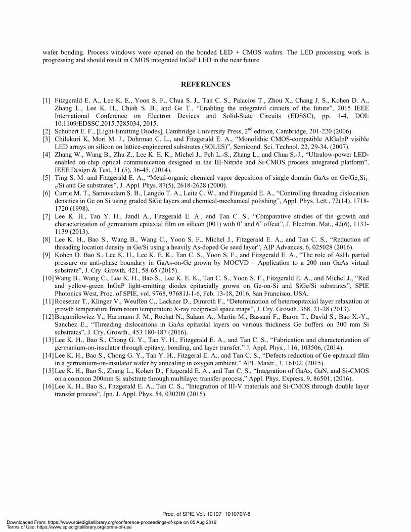
Because the InGaP LED layers are buried under the CMOS layer, windows have to be opened to expose the underneath device layers prior to LED processing. SiO2/SiNx/SiO2 tri-layers were deposited as hard mask. After RIE etching to form the hard mask, the underneath CMOS and bonding dielectric layers were etched. Figure 8 shows opened process trenches and the III-V films inside. Currently we are further processing the LED devices in the opened trenches.
We have also developed contacts without gold for the InGaP LEDs to comply with CMOS rules. Ni/Ge/Ni is used as the Ohmic contact with n-GaAs. The contact resistance is slightly higher than the standard Ni/Ge/Au/Ni/Au Ohmic contact for n-GaAs. For the Ohmic contact with p-GaAs, we are developing a Ti alloy. After we finish the LED processing, the wafers will be returned to a CMOS foundry service where the metal interconnections will be processed to connect the CMOS control circuits to the LEDs.
Figure 8. Photograph of a bonded CMOS + InGaP LED wafer after trench opening. The III-V area can be clearly seen. The InGaP LED processing will be done in the trenches.
4. SUMMARY In summary, we present our work on the integration of InGaP LEDs with CMOS circuitry on 200 mm silicon wafers. By applying compressive strain in the InGaP LED layers, 200 mm wafer bow was limited to less than 50 μm. The CMOS wafers were processed by a 200mm foundry service and successfully transferred to the InGaP LED wafers by double
Proc. of SPIE Vol. 10107 101070Y-7Downloaded From: https://www.spiedigitallibrary.org/conference-proceedings-of-spie on 05 Aug 2019Terms of Use: https://www.spiedigitallibrary.org/terms-of-use
wafer bonding. Process windows were opened on the bonded LED + CMOS wafers. The LED processing work is progressing and should result in CMOS integrated InGaP LED in the near future.
REFERENCES
[1] Fitzgerald E. A., Lee K. E., Yoon S. F., Chua S. J., Tan C. S., Palacios T., Zhou X., Chang J. S., Kohen D. A., Zhang L., Lee K. H., Chiah S. B., and Ge T., “Enabling the integrated circuits of the future”, 2015 IEEE International Conference on Electron Devices and Solid-State Circuits (EDSSC), pp. 1-4, DOI: 10.1109/EDSSC.2015.7285034, 2015.
[2] Schubert E. F., [Light-Emitting Diodes], Cambridge University Press, 2nd edition, Cambridge, 201-220 (2006). [3] Chilukuri K, Mori M. J., Dohrman C. L., and Fitzgerald E. A., “Monolithic CMOS-compatible AlGaInP visible
LED arrays on silicon on lattice-engineered substrates (SOLES)”, Semicond. Sci. Technol. 22, 29-34, (2007). [4] Zhang W., Wang B., Zhu Z., Lee K. E. K., Michel J., Peh L.-S., Zhang L., and Chua S.-J., “Ultralow-power LED-
enabled on-chip optical communication designed in the III-Nitride and Si-CMOS process integrated platform”, IEEE Design & Test, 31 (5), 36-45, (2014).
[5] Ting S. M. and Fitzgerald E. A., “Metal-organic chemical vapor deposition of single domain GaAs on Ge/GexSi1-
x/Si and Ge substrates”, J. Appl. Phys. 87(5), 2618-2628 (2000). [6] Currie M. T., Samavedam S. B., Langdo T. A., Leitz C. W., and Fitzgerald E. A., “Controlling threading dislocation
densities in Ge on Si using graded SiGe layers and chemical-mechanical polishing”, Appl. Phys. Lett., 72(14), 1718-1720 (1998).
[7] Lee K. H., Tan Y. H., Jandl A., Fitzgerald E. A., and Tan C. S., “Comparative studies of the growth and characterization of germanium epitaxial film on silicon (001) with 0˚ and 6˚ offcut”, J. Electron. Mat., 42(6), 1133-1139 (2013).
[8] Lee K. H., Bao S., Wang B., Wang C., Yoon S. F., Michel J., Fitzgerald E. A., and Tan C. S., “Reduction of threading location density in Ge/Si using a heavily As-doped Ge seed layer”, AIP Advances, 6, 025028 (2016).
[9] Kohen D. Bao S., Lee K. H., Lee K. E. K., Tan C. S., Yoon S. F., and Fitzgerald E. A., “The role of AsH3 partial pressure on anti-phase boundary in GaAs-on-Ge grown by MOCVD – Application to a 200 mm GaAs virtual substrate”, J. Cry. Growth. 421, 58-65 (2015).
[10] Wang B., Wang C., Lee K. H., Bao S., Lee K. E. K., Tan C. S., Yoon S. F., Fitzgerald E. A., and Michel J., “Red and yellow-green InGaP light-emitting diodes epitaxially grown on Ge-on-Si and SiGe/Si substrates”, SPIE Photonics West, Proc. of SPIE, vol. 9768, 97681J-1-6, Feb. 13-18, 2016, San Francisco, USA.
[11] Roesener T., Klinger V., Weuffen C., Lackner D., Dimroth F., “Determination of heteroepitaxial layer relaxation at growth temperature from room temperature X-ray reciprocal space maps”, J. Cry. Growth. 368, 21-28 (2013).
[12] Bogumilowicz Y., Hartmann J. M., Rochat N., Salaun A., Martin M., Bassani F., Baron T., David S., Bao X.-Y., Sanchez E., “Threading dislocations in GaAs epitaxial layers on various thickness Ge buffers on 300 mm Si substrates”, J. Cry. Growth., 453 180-187 (2016).
[13] Lee K. H., Bao S., Chong G. Y., Tan Y. H., Fitzgerald E. A., and Tan C. S., “Fabrication and characterization of germanium-on-insulator through epitaxy, bonding, and layer transfer,” J. Appl. Phys., 116, 103506, (2014).
[14] Lee K. H., Bao S., Chong G. Y., Tan Y. H., Fitzgeral E. A., and Tan C. S., “Defects reduction of Ge epitaxial film in a germanium-on-insulator wafer by annealing in oxygen ambient,” APL Mater., 3, 16102, (2015).
[15] Lee K. H., Bao S., Zhang L., Kohen D., Fitzgerald E. A., and Tan C. S., “Integration of GaAs, GaN, and Si-CMOS on a common 200mm Si substrate through multilayer transfer process,” Appl. Phys. Express, 9, 86501, (2016).
[16] Lee K. H., Bao S., Fitzgerald E. A., Tan C. S., "Integration of III-V materials and Si-CMOS through double layer transfer process", Jpn. J. Appl. Phys. 54, 030209 (2015).
Proc. of SPIE Vol. 10107 101070Y-8Downloaded From: https://www.spiedigitallibrary.org/conference-proceedings-of-spie on 05 Aug 2019Terms of Use: https://www.spiedigitallibrary.org/terms-of-use