Embed Size (px)
Citation preview
J.1
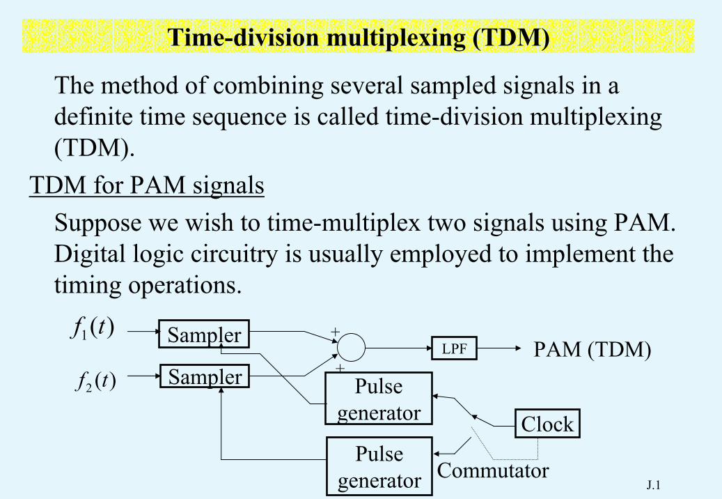
Time-division multiplexing (TDM)
The method of combining several sampled signals in a definite time sequence is called time-division multiplexing (TDM).
TDM for PAM signalsSuppose we wish to time-multiplex two signals using PAM. Digital logic circuitry is usually employed to implement the timing operations.
Sampler
Sampler Pulsegenerator
Pulsegenerator
LPF
Clock
PAM (TDM))(1 tf
)(2 tf
+
+
Commutator

J.2
The time-multiplexed PAM output is
Sampling rateThe sampling rate depends on the bandwidth of the signals. For example, if the signals are low-pass and band-limited to 3kHz. The sampling theorem states that each must be sampled at a rate no less than 6kHz. This requires a 12kHz minimum clock rate for the two-channel system.
t
)(1 tf)(2 tf
xT
T

J.3
Transmission bandwidth– The time-multiplexed PAM signal can be sent out on a
line (baseband communications) or used to modulate a transmitter (passband communications).
Theoretically, the bandwidth occupied by a pulse is infinite.

J.4
However, we are transmitting the information of the signals ( ), not the information of the pulses.
If the time spacing between adjacent samples is (In thisexample, ), the minimum bandwidth is
.
)(),( 21 tftf
xT2/TTx =
)2/(1 xx TB =

J.5
For example, if the time-multiplexed PAM signal described in J.4 is filtered with a low-pass filter with bandwidth
, the impulses become sinx/x terms.
Because we have chosen the spacing between successive samples to be , contributions from all adjacent channels are exactly zero at the correct sampling instant. Therefore, by sampling the output at the correct instant, one can exactly reconstruct the original sampled values
LPFt t
)2/(1 xB
)2/(1 xx BT =
)2/(1 xB

J.6
t
)(1 tf
)(2 tf
xT
T
tLPF
The results refer to the case in which impulse sampling and ideal filtering. In practice, neither of these conditions can beachieved and wider bandwidth is required.
The required bandwidth depends on the allowable cross-talk (interference) between channels.

J.7
Receiver
Synchronization of the the clock and the commutator in the time-multiplex receiver can be achieved by sending some pre-assigned code which, when identified at the receiver, serves to synchronize the timing.
Sampler
Sampler
Pulsegenerator
Clock
)(tfPAM
Commutator
LPF
LPF
)(1 tf
)(2 tf
Pulsegenerator

J.8
After time multiplexing and filtering, the pulse-modulated waveform may be transmitted directly on a pair of wire lines
For long distance transmission, the multiplexed signal is used as the modulating signal to modulate a carrier.– For example, PAM/AM
PAMmultiplexer
Clock
AMmodulator
tcωcos
AMdemodulator
tcωcos
PAMmultiplexer
Clock

J.9
Advantages of TDM– high reliability and efficient operation as the circuitry
required is digital.– Relatively small interchannel cross-talk arising from
nonlinearities in the amplifiers that handle the signals in the transmitter and receiver.
Disadvantages of TDM– timing jitter

J.10
ExampleChannel 1 of a two-channel PAM system handles 0-8 kHz signals; the second channel handles 0-10kHz signals. The two channels are sampled at equal intervals of time using very narrow pulses at the lowest frequency that is theoretically adequate.
Sampler
Sampler
Pulsegenerator
Pulsegenerator
LPF
Clock
PAM (TDM))(1 tf
)(2 tf
+
+
Commutator

J.11
a) what is the minimum clock frequency of the PAM signal ?The minimum sampling rate for channel 1 is 2B = 16kHz.The minimum sampling rate for channel 2 is 20kHz.
In order to sample channel 2 adequately, we must take samples at a 20kHz rate. Therefore the commutator clock rate is 40kHz.

J.12
b) What is the minimum cutoff frequency of the low-pass filter used before transmission that will preserve the amplitude information on the output pulses ?
c) What would be the minimum bandwidth if these channel were frequency multiplexed, using normal AM techniques and SSB techniques ?AM: 2*(bandwidth of channel 1) + 2*(bandwidth of
channel 2) = 2*8kHz + 2*10kHz = 36kHz
SSB: bandwidth of channel 1 + bandwidth of channel 2 = 8kHz + 10kHz = 18kHz
kHzTB xx 20)2/(1 =≥

J.13
d) Assume the signal in channel 1 is sin(5000πt) and that in channel 2 is sin(10000πt). Sketch these signals; sketch the waveshapes at the input to the first low-pass filter, at the filter output, and at the output of the sample-and-hold circuit and output of the low-pass filter in channel 2.
t
ms4.0
)5000sin( tπt
ms2.0
)10000sin( tπ

J.14
Sampling period = 1/(2*10kHz)=0.05ms
Multiplexed PAM:
Output of filter:
t
ms4.0
ms05.0tms05.0
ms2.0
t
t

J.15
Output of holding circuitfor channel 2:
Output of low-pass filter:
t
t

J.16
Return-to-bias (RB) method– Three levels are used: 0,1, and a bias level.– Bias level may be chosen either below or between the
other two levels.– The waveform returns to the bias level during the last half
of each bit interval.– The RB method has an advantage in being self-clocking.
1 1 1 0 0 1 PCM code
RB
Example:1 ==> A volts0 ==> -A volts
Line coding

J.17
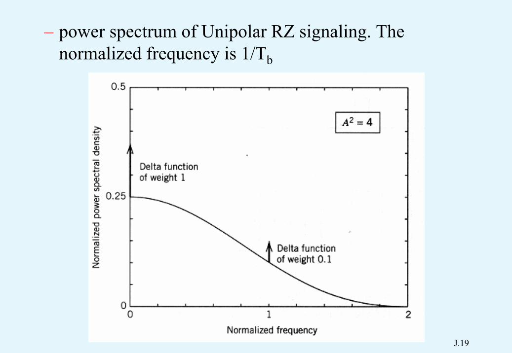
Unipolar Return-to-zero (RZ) method– Digit ‘1’ is represented by a change to the 1 level for one-half the
bit interval, after which the signal returns to the reference level for the remaining half-bit interval.
– Digit ‘0’ is indicated by no change, the signal remaining at thereference level.
– Its disadvantage is that it requires 3dB more power than RB signaling (or AMI) for the same probability of symbol error.
– An attractive feature of this line code is the presence of deltafunction at f=1/Tb in the power spectrum of the transmitted signal, which can be used for bit-timing recovery at the receiver.

J.18
1 1 1 0 0 1 PCM code
RZ
RB
Tb :Bit duration
Decision boundary
J.19
– power spectrum of Unipolar RZ signaling. The normalized frequency is 1/Tb

J.20
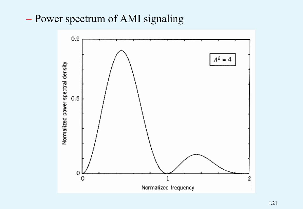
Alternate Mark Inversion (AMI)– The first ‘1’ is represented by +1, the second ‘1’ by -1,
the third ‘1’ by +1, etc.– has zero average value and relatively insignificant low-
frequency components– used in telephone PCM systems.– Also referred to as a bipolar return-to-zero (BRZ)
representation.
1 1 1 0 0 1 PCM code
AMI
J.21
– Power spectrum of AMI signaling

J.22
Spilt phase– eliminates the variation in average value using symmetry.– In the Manchester split-phase method
• A ‘1’ is represented by a 1 level during the first half-bit interval, then shifted to 0 level for the latter half-bit interval
• A ‘0’ is indicated by the reverse representation.
– The manchester code suppresses the DC component and has relatively insignificant low-frequency components.
– In the split-phase (mark) method, a similar symmetric representation is used except that a phase reversal relative to the previous phase indicates a ‘1’ and no change is used to indicate a ‘0’.

J.23
1 1 1 0 0 1 PCM code
Split-phase (Manchester)
Split-phase (mark)

J.24
– Power spectrum of Manchester code signaling

J.25
Nonreturn-to-zero– reduce the bandwidth needed to send the PCM code.– In the NRZ(L) representation, a bit pulse remains in one of its two
levels for the entire bit interval. – In the NRZ(M) method a level change is used to indicate a ‘1’ and
no level change for a ‘0’.– In the NRZ(S) method a level change is used to indicate a ‘0’ and
no level change for a ‘1’.– NRZ representations require added receiver complexity to
determine the clock frequency.1 1 1 0 0 1 PCM code
NRZ (L)
NRZ (M)
NRZ (S)
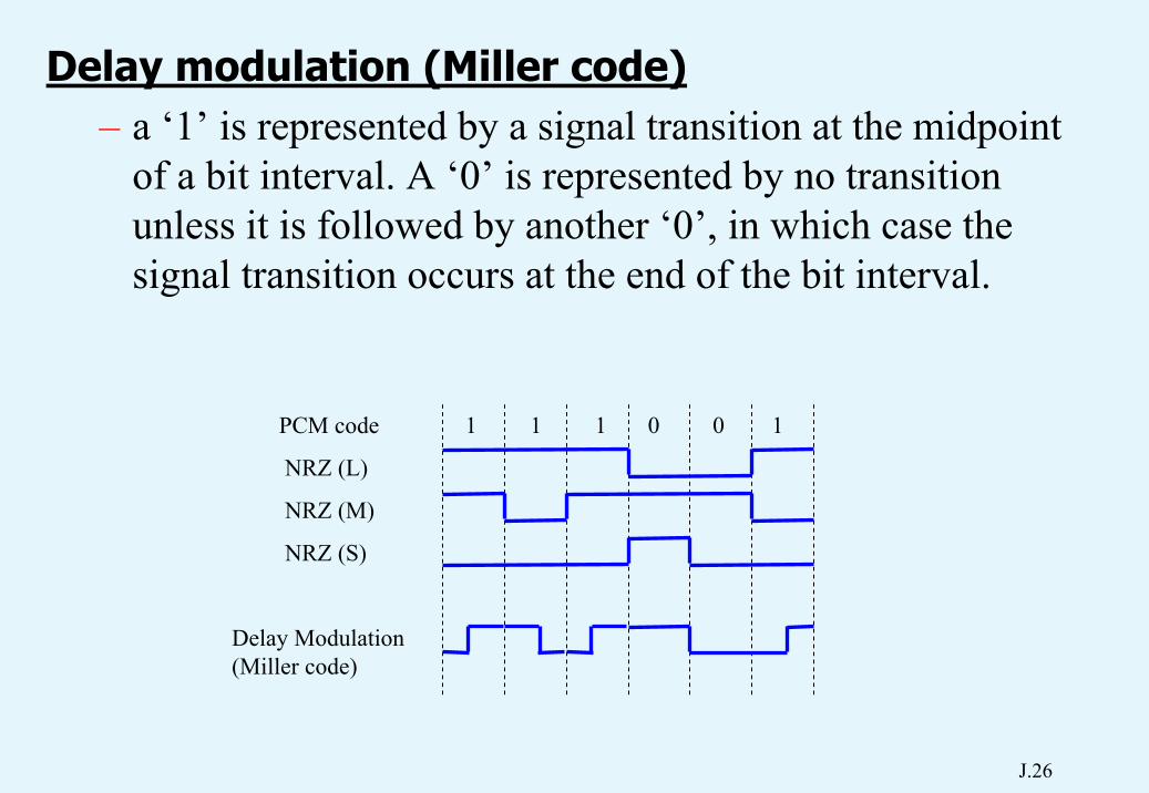
Delay Modulation (Miller code)
J.26
Delay modulation (Miller code)– a ‘1’ is represented by a signal transition at the midpoint
of a bit interval. A ‘0’ is represented by no transition unless it is followed by another ‘0’, in which case the signal transition occurs at the end of the bit interval.
1 1 1 0 0 1 PCM code
NRZ (L)
NRZ (M)
NRZ (S)
Delay Modulation (Miller code)

J.27
– Power spectrum of NRZ(L)

J.28
Transmission bandwidth– The fundamental frequency of a binary code stream depends on its most rapidly varying
pattern.– Example: ‘111’ for RZ and NRZ(M)
– For a binary PCM system with n quantization levels, the number of bits per sample is
– If the sample rate be 1/T, then the number of bits per second to be sent is
– The minimum bandwidth is
(NRZ) (RZ)
1 1 1 1 1 1
bT bTbo Tf /1= bo Tf 2/1=
[ ]n2log (the brackets indicate the next higher integer to be taken, e.g. if n=7, we use 3 bits)
[ ] Tn /log2
[ ]
≥
TnB 2log
21 [ ]
TnB 2log
≥
J.29
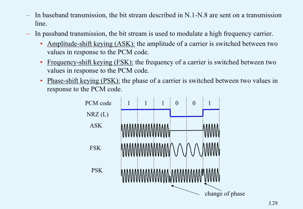
– In baseband transmission, the bit stream described in N.1-N.8 are sent on a transmission line.
– In passband transmission, the bit stream is used to modulate a high frequency carrier.• Amplitude-shift keying (ASK): the amplitude of a carrier is switched between two
values in response to the PCM code.• Frequency-shift keying (FSK): the frequency of a carrier is switched between two
values in response to the PCM code.• Phase-shift keying (PSK): the phase of a carrier is switched between two values in
response to the PCM code.
1 1 1 0 0 1 PCM code
NRZ (L)
ASK
FSK
PSK
change of phase

J.30
– PSK and FSK are preferred to ASK signals for passbanddata transmission over nonlinear channel such as micorwave link and satellite channels.
Coherent and Noncoherent
– Digital modulation techniques are classified into coherent and noncoherent techniques, depending on whether the receiver is equipped with a phase-recovery circuit or not.
– The phase-recovery circuit ensures that the local oscillator in the receiver is synchronized to the incoming carrier wave (in both frequency and phase).
J.31
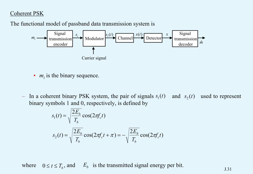
Coherent PSK
The functional model of passband data transmission system is
• mi is the binary sequence.
– In a coherent binary PSK system, the pair of signals and used to represent binary symbols 1 and 0, respectively, is defined by
where , and is the transmitted signal energy per bit.
ModulatorSignal
transmission encoder
im
Carrier signal
)(tsi Channel)(tx
Detectoris x Signal transmission
decoder m̂
)(1 ts )(2 ts
)2cos(2)(1 tfTEts cb
b π=
)2cos(2)2cos(2)(2 tfTEtf
TEts c
b
bc
b
b πππ −=+=
bTt ≤≤0 bE

J.32
For example,
To ensure that each transmitted bit contains an integral number of cycles of the carrier wave, the carrier frequency is chosen equal to for some fixed integer n.
The transmitted signal can be written as
and
where
[ ] bb
b
bT
cb
bT
ETTEdttf
TEdttsE
bb=⋅=== ∫∫ 2
2)2(cos2)(0
2
0
21 π
cf bTn /
)()(1 tEts bφ=
)()(2 tEts bφ−=
bcb
b TttfT
t <≤= 0 )2cos(2)( πφ
)2cos(2)(
)2cos(2)2cos(2)(
1
1
π
ππ
nTETs
tTn
TEtf
TEts
b
bb
bb
bc
b
b
=∴
==
J.33
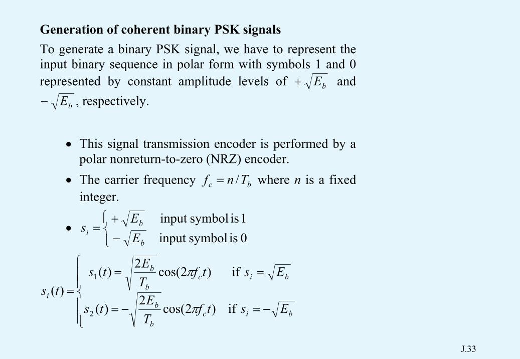
Generation of coherent binary PSK signalsTo generate a binary PSK signal, we have to represent theinput binary sequence in polar form with symbols 1 and 0represented by constant amplitude levels of bE+ and
bE− , respectively.
• This signal transmission encoder is performed by apolar nonreturn-to-zero (NRZ) encoder.
• The carrier frequency bc Tnf /= where n is a fixedinteger.
•
−+
=0 is symbolinput 1 is symbolinput
b
bi E
Es
−=−=
===
bicb
b
bicb
b
i
EstfTEts
EstfTEts
ts if)2cos(2)(
if)2cos(2)()(
2
1
π
π

J.34
ProductModulator
Signal transmission
encoder
10101 is
)2cos(2)( tfT
t cb
πφ =
)(tsi

J.35
Detection of coherent binary PSK signalsTo detect the original binary sequence of 1s and 0s, weapply the noisy PSK signal to a correlator. The correlatoroutput is compared with a threshold of zero volts.
∫bT
0)(tx
)(tφ
Correlator
X1x Decision
device
0
if 0 if 1
1
1
xx

J.36
Example: If the transmitted symbol is 1,
)2cos(2)( tfTEtx cb
b π=
and the correlator output is
b
T
cb
b
T
cb
cb
b
T
E
dttfT
E
dttfT
tfTE
dtttxx
b
b
b
=
⋅=
⋅=
=
∫
∫
∫
0
2
0
01
)2(cos2
)2cos(2)2cos(2
)()(
π
ππ
φ
Similarly, If the transmitted symbol is 0, bEx −=1 .

J.37
Delta Modulation (DM) and Differential Pulse Code Modulation (DPCM)
Reference– Stremler, Communication Systems, Chapter 9.7
Delta Pulse Code Modulation (DPCM)– In the transmission of messages having repeated sample values, the repeated
transmission represents a waste of communication capability because there is little information content in the repeated values.
– In DPCM, only the digitally encoded difference between successive sample values. Therefore, the number of bit can be reduced.
– Example: a picture that has been quantized to 6 bits can be transmitted with comparable quality using 4-bit DPCM.

J.38
LPF)(tf
Decoder
Clock/Sampler
Quantizer-encoder
∫
+-
DPCM
Decoder ∫ LPFDPCM )(tf≈
)(tf)(tfLP
)(tfLP
t t
)(tg
)(tfdelay
)()( Ttftf LPdelay −≈
)()()( tftftg delayLP −=
t
Range of > Range of )(tf )(tg

J.39
Delta Modulation (DM)– In delta modulation (DM), an incoming signal is oversampled (i.e. at a rate much
higher than the Nyquist rate) to purposely increase the correlation between adjacent samples of the signal.
– The difference between the input and the approximation is quantized into two levels:
∆±
>+∆−>+∆+
=+)()( if)()()( if)(
)(nTfTnTfnTfnTfTnTfnTf
TnTfqq
qqq
)( TnTf +
Delay T
Quantizer+
-+
+
Encoder
)(nTfq
)( TnTfq +
DM
Accumulator

J.40
– Disadvantages• If the input signal level remains constant, the reconstructed DM waveform
exhibits a hunting behavior known as idling noise.• Slope-overload
)(tf
t
t
0 1 0 1 1 0 1 0 1 1 1 1 1 0 1
Idling noiseSlope-overload


![WorkinProgress: ANewApproachtoStudentLearningofReal ......DigiScope are a library of sampled ECG signals from the PhysioNet ECG database [1]. Once a filter is designed in DigiScope](https://img.pdfslide.net/doc/110x75/5e8eb63b10d1c91b4836c19d/workinprogress-anewapproachtostudentlearningofreal-digiscope-are-a-library.jpg)


![FlexStylus: Leveraging Bend Input for Pen Interaction FlexStylus: Leveraging Bend Input for Pen Interaction ... [13] created Twend, a planar, cellphone- ... signals are sampled by](https://img.pdfslide.net/doc/110x75/5b49c20c7f8b9a691e8b9f02/flexstylus-leveraging-bend-input-for-pen-flexstylus-leveraging-bend-input-for.jpg)