Embed Size (px)
Citation preview
07) 2000–2003www.elsevier.com/locate/matlet
Materials Letters 61 (20
The optical properties of ZnO sheets electrodeposited on ITO glass
Feifei Wang a,b, Ruibin Liu a,b, Anlian Pan a,b, Li Cao a,b, Ke Cheng a,b, Bofei Xue a, Geng Wang c,Qingbo Meng a, Jinghong Li c, Qi Li b, Yanguo Wang a,b,
Taihong Wang a,b, Bingsuo Zou a,b,⁎
a Institute of Physics, Chinese Academy of Sciences, Beijing 100080, Chinab Micro–Nano Technologies Research Center, Hunan University, Changsha 410082, China
c Department of chemistry, Tsinghua University, Beijing 100084, China
Received 13 February 2006; accepted 1 August 2006Available online 28 August 2006
Abstract
Large-scale hexagonal ZnO sheets were grown on ITO glass by cathodic electrodeposition in an aqueous zinc nitrate/potassium chloride solution at60 °C and annealing at 350 °C for an hour. The sheets are about 3μm indimension and 100–300 nm in thickness. TheZnO sheets showmany nano-pits onthe surface and produce intense green luminescence at room temperature under femtosecond (fs) pulse ultraviolet (UV) light excitation. Both power-dependent photoluminescence spectra and time-resolved spectra weremeasuredwith varied excitation powers. Lasing phenomena occur at above 500 μJ/cm2 and the stimulated emission occurs with lifetime of less than 30 ps over 600 μJ/cm2. Additionally, the open-circuit photovoltage spectra indicate thatthe light-absorbing dye of RuL2(NCS)2 (N3) can be well adsorbed on the surface of ZnO sheets, which is useful for the dye-sensitized solar cells(DSSC).© 2006 Elsevier B.V. All rights reserved.
1. Introduction
With large band gap (3.3–3.6 eV) and high exciton bindingenergy (60meV), ZnOhas been recognized as an excellentmaterialfor UV lasers. Besides, ZnO has many potential applications insensors, photocatalysis, field emission, and solar cells [1–5]. Inrecent years, different patterns of ZnO [6–13], such as nanojunctionarrays, nanobelt, nanospring, nanoring, nanosheets, etc, have beenreported. The methods used to prepare ZnO nanostructures includePLD, MBE, CVD, MOCVD, and wet chemical technique, butsome of these equipments are expensive and the operationprocedures are rather complicated. Electrodeposition presentsseveral advantages over the above techniques with low cost,simple operation, and wide compatibility. The deposition processcan be carried out on various substrates [14], such as glass,polymer, semiconductor, and template. There is no more specialrequirement needed for the substrate, except that it's conductive, sothis technique is well adapted for industrial procedures. Further-more, the thickness, alignment and morphology of the deposited
⁎ Corresponding author. Institute of Physics, Chinese Academy of Sciences,Beijing 100080, China.
E-mail address: [email protected] (B. Zou).
0167-577X/$ - see front matter © 2006 Elsevier B.V. All rights reserved.doi:10.1016/j.matlet.2006.08.007
films/sheets can be controlled to a certain degree by altering theexperimental conditions and substrate structure. In electrodeposi-tion, the growth proceeds by electron injection from the electrode;therefore, a reasonable electronic contact was formed at theinterface of the deposited film and the electrode, which isadvantageous for specific applications.
In this paper, we report on the preparation of ZnO nanosheetson ITO glass by cathodic electrodeposition in an aqueous zincnitrate solution and studied their optical properties. Thestimulated emission of ZnO thin films, nanowires, single nano-belts, nanorod arrays have been reported [15–21], however, thestimulated emission behavior of ZnO sheets prepared byelectrodeposition procedure are rather sparsely studied. Further-more, N3 shows strong adsorption on the annealed ZnO surfacewithmany nano-pits andwhichmakes ZnO possible to be appliedto the dye-sensitized solar cells. The experiment data indicatesthat the as-developed ZnO sheets might have significantapplications in photonics and photoelectric devices.
2. Experiments
ZnO nanosheets were grown by electrodeposition on ITOglass. The electrodeposition procedure involved a standard three-
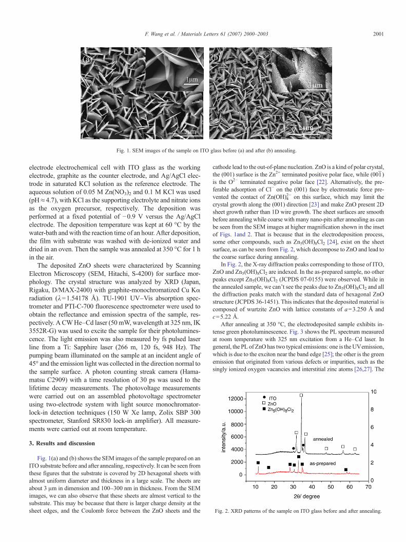
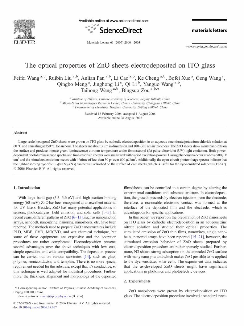
Fig. 1. SEM images of the sample on ITO glass before (a) and after (b) annealing.
Fig. 2. XRD patterns of the sample on ITO glass before and after annealing.
2001F. Wang et al. / Materials Letters 61 (2007) 2000–2003
electrode electrochemical cell with ITO glass as the workingelectrode, graphite as the counter electrode, and Ag/AgCl elec-trode in saturated KCl solution as the reference electrode. Theaqueous solution of 0.05 M Zn(NO3)2 and 0.1 M KCl was used(pH≈4.7), with KCl as the supporting electrolyte and nitrate ionsas the oxygen precursor, respectively. The deposition wasperformed at a fixed potential of −0.9 V versus the Ag/AgClelectrode. The deposition temperature was kept at 60 °C by thewater-bath andwith the reaction time of an hour. After deposition,the film with substrate was washed with de-ionized water anddried in an oven. Then the sample was annealed at 350 °C for 1 hin the air.
The deposited ZnO sheets were characterized by ScanningElectron Microscopy (SEM, Hitachi, S-4200) for surface mor-phology. The crystal structure was analyzed by XRD (Japan,Rigaku, D/MAX-2400) with graphite-monochromatized Cu Kαradiation (λ=1.54178 Å). TU-1901 UV–Vis absorption spec-trometer and PTI-C-700 fluorescence spectrometer were used toobtain the reflectance and emission spectra of the sample, res-pectively. A CWHe–Cd laser (50 mW, wavelength at 325 nm, IK3552R-G) was used to excite the sample for their photolumines-cence. The light emission was also measured by fs pulsed laserline from a Ti: Sapphire laser (266 m, 120 fs, 948 Hz). Thepumping beam illuminated on the sample at an incident angle of45° and the emission light was collected in the direction normal tothe sample surface. A photon counting streak camera (Hama-matsu C2909) with a time resolution of 30 ps was used to thelifetime decay measurements. The photovoltage measurementswere carried out on an assembled photovoltage spectrometerusing two-electrode system with light source monochromator-lock-in detection techniques (150 W Xe lamp, Zolix SBP 300spectrometer, Stanford SR830 lock-in amplifier). All measure-ments were carried out at room temperature.
3. Results and discussion
Fig. 1(a) and (b) shows the SEM images of the sample prepared on anITO substrate before and after annealing, respectively. It can be seen fromthese figures that the substrate is covered by 2D hexagonal sheets withalmost uniform diameter and thickness in a large scale. The sheets areabout 3 μm in dimension and 100–300 nm in thickness. From the SEMimages, we can also observe that these sheets are almost vertical to thesubstrate. This may be because that there is larger charge density at thesheet edges, and the Coulomb force between the ZnO sheets and the
cathode lead to the out-of-plane nucleation. ZnO is a kind of polar crystal,the (001) surface is the Zn2+ terminated positive polar face, while (001̄)is the O2− terminated negative polar face [22]. Alternatively, the pre-ferable adsorption of Cl− on the (001) face by electrostatic force pre-vented the contact of Zn(OH)4
2− on this surface, which may limit thecrystal growth along the (001) direction [23] and make ZnO present 2Dsheet growth rather than 1D wire growth. The sheet surfaces are smoothbefore annealing while coarse with many nano-pits after annealing as canbe seen from the SEM images at higher magnification shown in the insetof Figs. 1and 2. That is because that in the electrodeposition process,some other compounds, such as Zn5(OH)8Cl2 [24], exist on the sheetsurface, as can be seen from Fig. 2, which decompose to ZnO and lead tothe coarse surface during annealing.
In Fig. 2, the X-ray diffraction peaks corresponding to those of ITO,ZnO and Zn5(OH)8Cl2 are indexed. In the as-prepared sample, no otherpeaks except Zn5(OH)8Cl2 (JCPDS 07-0155) were observed. While inthe annealed sample, we can't see the peaks due to Zn5(OH)8Cl2 and allthe diffraction peaks match with the standard data of hexagonal ZnOstructure (JCPDS 36-1451). This indicates that the deposited material iscomposed of wurtzite ZnO with lattice constants of a=3.250 Å andc=5.22 Å.
After annealing at 350 °C, the electrodeposited sample exhibits in-tense green photoluminescence. Fig. 3 shows the PL spectrum measuredat room temperature with 325 nm excitation from a He–Cd laser. Ingeneral, the PL of ZnO has two typical emissions: one is theUVemission,which is due to the exciton near the band edge [25]; the other is the greenemission that originated from various defects or impurities, such as thesingly ionized oxygen vacancies and interstitial zinc atoms [26,27]. The
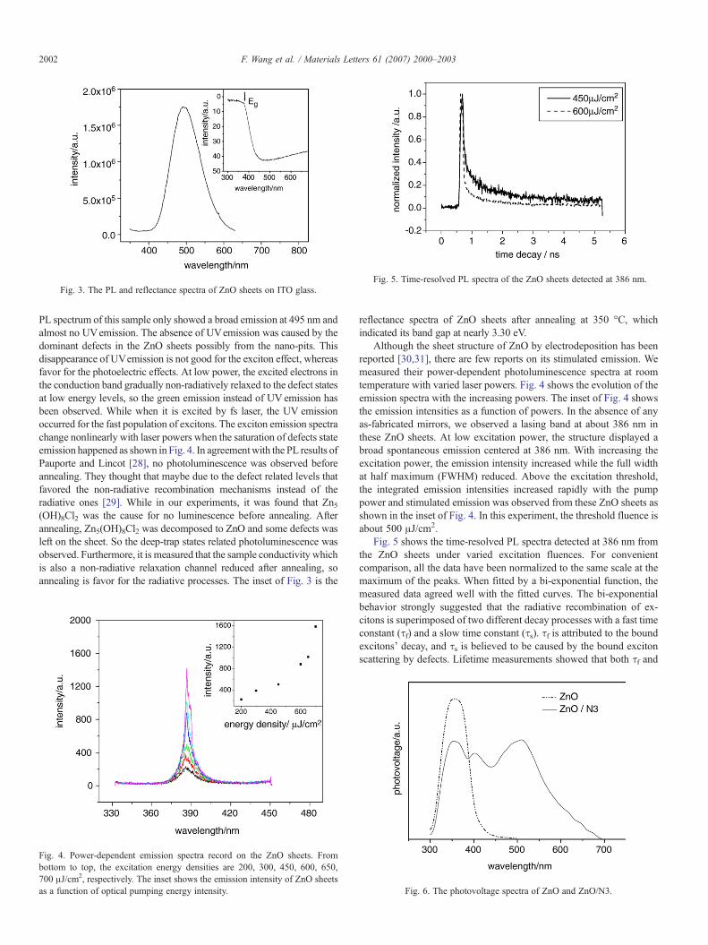
Fig. 5. Time-resolved PL spectra of the ZnO sheets detected at 386 nm.Fig. 3. The PL and reflectance spectra of ZnO sheets on ITO glass.
2002 F. Wang et al. / Materials Letters 61 (2007) 2000–2003
PL spectrum of this sample only showed a broad emission at 495 nm andalmost no UVemission. The absence of UVemission was caused by thedominant defects in the ZnO sheets possibly from the nano-pits. Thisdisappearance of UVemission is not good for the exciton effect, whereasfavor for the photoelectric effects. At low power, the excited electrons inthe conduction band gradually non-radiatively relaxed to the defect statesat low energy levels, so the green emission instead of UV emission hasbeen observed. While when it is excited by fs laser, the UV emissionoccurred for the fast population of excitons. The exciton emission spectrachange nonlinearly with laser powers when the saturation of defects stateemission happened as shown in Fig. 4. In agreementwith the PL results ofPauporte and Lincot [28], no photoluminescence was observed beforeannealing. They thought that maybe due to the defect related levels thatfavored the non-radiative recombination mechanisms instead of theradiative ones [29]. While in our experiments, it was found that Zn5(OH)8Cl2 was the cause for no luminescence before annealing. Afterannealing, Zn5(OH)8Cl2 was decomposed to ZnO and some defects wasleft on the sheet. So the deep-trap states related photoluminescence wasobserved. Furthermore, it is measured that the sample conductivity whichis also a non-radiative relaxation channel reduced after annealing, soannealing is favor for the radiative processes. The inset of Fig. 3 is the
Fig. 4. Power-dependent emission spectra record on the ZnO sheets. Frombottom to top, the excitation energy densities are 200, 300, 450, 600, 650,700 μJ/cm2, respectively. The inset shows the emission intensity of ZnO sheetsas a function of optical pumping energy intensity.
reflectance spectra of ZnO sheets after annealing at 350 °C, whichindicated its band gap at nearly 3.30 eV.
Although the sheet structure of ZnO by electrodeposition has beenreported [30,31], there are few reports on its stimulated emission. Wemeasured their power-dependent photoluminescence spectra at roomtemperature with varied laser powers. Fig. 4 shows the evolution of theemission spectra with the increasing powers. The inset of Fig. 4 showsthe emission intensities as a function of powers. In the absence of anyas-fabricated mirrors, we observed a lasing band at about 386 nm inthese ZnO sheets. At low excitation power, the structure displayed abroad spontaneous emission centered at 386 nm. With increasing theexcitation power, the emission intensity increased while the full widthat half maximum (FWHM) reduced. Above the excitation threshold,the integrated emission intensities increased rapidly with the pumppower and stimulated emission was observed from these ZnO sheets asshown in the inset of Fig. 4. In this experiment, the threshold fluence isabout 500 μJ/cm2.
Fig. 5 shows the time-resolved PL spectra detected at 386 nm fromthe ZnO sheets under varied excitation fluences. For convenientcomparison, all the data have been normalized to the same scale at themaximum of the peaks. When fitted by a bi-exponential function, themeasured data agreed well with the fitted curves. The bi-exponentialbehavior strongly suggested that the radiative recombination of ex-citons is superimposed of two different decay processes with a fast timeconstant (τf) and a slow time constant (τs). τf is attributed to the boundexcitons' decay, and τs is believed to be caused by the bound excitonscattering by defects. Lifetime measurements showed that both τf and
Fig. 6. The photovoltage spectra of ZnO and ZnO/N3.
2003F. Wang et al. / Materials Letters 61 (2007) 2000–2003
τs became shorter while the amplitude of τf became larger withincreasing excitation power. The τf, τs and the amplitude of τf were0.086 ns, 1.0682 ns, and 85% for 450 μJ/cm2, and 0.053 ns, 0.9587 ns,and 92.8% for 600 μJ/cm2. This variation clearly shows that the boundexcitons were the origin of stimulated emission, which is different fromthe excitons emission reported in ZnO nanowire [32]. In furtherincreasing the excitation power, the decay time exceeded the streakcamera time resolution limit (30 ps). The ultra-short lifetime (b30 ps)and enhanced emission intensity with excitation fluences also indicatethat the giant oscillator strength [33,34] of bound excitons was thecause of stimulated emission. In contrast to the laser emission of ZnOnanowire [32], we can only observe the dominant emission at about386 nm in our sample, that is a clear indication of dominant metastablebound excitons. The high excitation threshold and long lifetime tailalso indicate a strong lattice scattering with these bound excitons.
The sample after annealing had much larger surface area due tonano-pits than the usual flat surface. This made it has potential appli-cation in dye-sensitized solar cell. We immersed the ZnO film in a N3ethanol solution for 10 h then let it dry naturally. The photovoltagespectra of both pure ZnO film and ZnO/N3 film were measured. Asshown in Fig. 6, the ZnO film showed an obvious photovoltage band at300–425 nm, which was due to the transition from valence band toconduction band. When the film was sensitized by N3, two additionalphotovoltage bands at about 402 nm and 514 nm appeared which weresimilar to the photoresponse of N3 [35]. It can be seen that the dye-sensitized film extended the photovoltaic signal to the whole visiblespectral range. This result together with its hardly observed excitonemission indicated that the ZnO/N3 film may be a good material fordye-sensitized solar cells. Further studies are underway.
4. Conclusions
In summary, hexagonal ZnO sheets with almost uniform sizewere obtained on ITO glass by electrodeposition and annealing.Its structure and composition is characterized, the sheet wasalmost vertical to the substrate and contains many nano-pits on itssurface. Stimulated emission, related to the bound excitons, wasobserved with increasing excitation powers at room temperature.Above the threshold power density (500 μJ/cm2), the emissionintensities increase quickly and lead to stimulated emission. Inaddition, the ZnO film adsorbed by N3 showed well-structuredphotovoltage responses in the visible range, and that made itpotentially applicable in dye-sensitized solar cells.
Acknowledgments
The authors thank the financial supports of NSFC of China(Term no. 20173073), National 973 project (2002CB713802),and Nanodevice key project of CAS.
References
[1] K. Hara, T. Horiguchi, T. Kinoshita, K. Sayama, H. Sugihara, H. Arakawa,Sol. Energy Mater. Sol. Cells 64 (2000) 115.
[2] J.A. Rodriguez, T. Jirsak, J. Dvorak, S. Sambasivan, D. Fischer, J. Phys.Chem., B 104 (2000) 319.
[3] H. Yumoto, T. Inoue, S.J. Li, T. Sako, K. Nishiyama, Thin Solid Films 345(1999) 38.
[4] C. Liu, J.A. Zapien, Y. Yao, X. Meng, C.S. Lee, S. Fan, Y. Lifshitz, S.T. Lee,Adv. Mater. 15 (2003) 838.
[5] E. Hosono, S. Fujihara, I. Honma, H. Zhou, Adv. Mater. 17 (2005) 2091.[6] P.X. Gao, Z.L. Wang, J. Phys. Chem., B 106 (2002) 12653.[7] J.Y. Lao, J.G. Wen, Z.F. Ren, Nano Lett. 2 (2002) 1287.[8] P.X. Gao, Y. Ding, Z.L. Wang, Nano Lett. 3 (2003) 1315.[9] X.Y. Kong, Z.L. Wang, Nano Lett. 3 (2003) 1625.[10] X.Y. Kong, Y. Ding, R.S. Yang, Z.L. Wang, Science 303 (2004) 1348.[11] C.X. Xu, X.W. Sun, Z.L. Dong, M.B. Yu, Appl. Phys. Lett. 85 (2004)
3878.[12] F. Li, Y. Ding, P.X. Gao, X.Q. Xin, Z.L. Wang, Angew. Chem., Int. Ed.
Engl. 43 (2004) 5238.[13] B.Q. Cao, W.P. Cai, Y. Li, F.Q. Sun, L.D. Zhang, Nanotechnology 16
(2005) 1734.[14] R. Könenkamp, K. Boedecker, M.C. Lux-Steiner,M. Poschenrieder, F. Zenia,
C. Leavy-Clement, Appl. Phys. Lett. 77 (2000) 2575.[15] D.M. Bagnall, Y.F. Chen, Z. Zhu, T. Yao, S. Koyama, M.Y. Shen, T. Goto,
Appl. Phys. Lett. 70 (1997) 2230.[16] Z.K. Tang, G.K.L. Wong, P. Yu, M. Kawasaki, A. Ohtomo, H. Koinuma,
Y. Segawa, Appl. Phys. Lett. 72 (1998) 3270.[17] H. Cao, Y.G. Zhao, H.C. Ong, S.T. Ho, J.Y. Dai, J.Y. Wu, R.P.H. Chang,
Appl. Phys. Lett. 73 (1998) 3656.[18] M.H. Huang, S. Mao, H. Feick, H.Q. Yan, Y.Y. Wu, H. Kind, E. Weber,
R. Russo, P.D. Yang, Science 292 (2001) 1897.[19] C.H. Liu, J.A. Zapien, Y. Yao, X.M. Meng, C.S. Lee, S.S. Fan, Y. Lifshitz,
S.T. Lee, Adv. Mater. 15 (2003) 838.[20] H.Q. Yan, J. Johnson, M. Law, R.R. He, K. Knutsen, J.R. McKinney,
J. Pham, R. Saykally, P.D. Yang, Adv. Mater. 15 (2003) 1907.[21] X.H. Han, G.Z. Wang, Q.T. Wang, L. Cao, R.B. Liu, B.S. Zou, J.G. Hou,
Appl. Phys. Lett. 86 (2005) 223106.[22] Z.L. Wang, X.Y. Kong, J.M. Zou, Phys. Rev. Lett. 91 (2003) 185502.[23] L.F. Xu, Y. Guo, Q. Liao, J.P. Zhang, D.S. Xu, J. Phys. Chem., B 109
(2005) 13519.[24] M.H. Wong, A. Berenov, X. Qi, M.J. Kappers, Z.H. Barber, B. Illy, Z.
Lockman, M.P. Ryan, J.L. MacManus-Driscoll, Nanotechnology 14(2003) 968.
[25] Y.C. Kong, D.P. Yu, B. Zhang, W. Fang, S.Q. Feng, Appl. Phys. Lett. 78(2001) 407.
[26] K. Vanheusden, W.L. Warren, C.H. Seager, D.R. Tallant, J.A. Voigt, B.E.Gnade, J. Appl. Phys. 79 (1996) 7983.
[27] E.G. Bylander, J. Appl. Phys. 49 (1978) 1188.[28] T. Pauporte, D. Lincot, Appl. Phys. Lett. 75 (1999) 2861.[29] J. Cembrero, A. Elmanouni, B. Hartiti, M. Mollar, B. Mar, Thin Solid
Films 451 (2004) 198.[30] L.F. Xu, Y. Guo, Q. Liao, J.P. Zhang, D.S. Xu, J. Phys. Chem., B 109
(2005) 13519.[31] B. Illy, B.A. Shollock, J.L. MacManus-Driscoll, M.P. Ryan, Nanotech-
nology 16 (2005) 320.[32] L. Cao, B.S. Zou, C.R. Li, Z.B. Zhang, S.S. Xie, G.Z. Yang, Europhys.
Lett. 68 (2004) 740.[33] E. Hanamura, Phys. Rev., B 37 (1988) 1273.[34] T. Takagahara, E. Hanamura, Phys. Rev. Lett. 56 (1986) 2533.[35] M.K. Nazeeruddin, A. Kay, I. Rodicio, R. Humpbry-Baker, E. Miiller, P.
Liska, N. Vlachopoulos, M. Gratzel, J. Am. Chem. Soc. 115 (1993) 6382.