Embed Size (px)
Citation preview

The Spin Field-Effect Transistor: Can It Be Realized?
Hiwa Modarresi* * Zernike Institute for Advanced Materials, University of Groningen, Nijenborgh 4, 9747 AG Groningen, the Netherlands
Supervisor: Caspar van der Wal
(Submitted to Erik Van der Giessen: June 1st, 2009)
Abstract
If it is realized, the proposed spin field-effect transistor can revolutionize the way all existing
transistor-based devices work through the implementation of a faster and a more efficient
performance accompanied by other advantages like non-volatility of data storage, less heat
generation, and smaller space occupation. It is now more than two decades that the question
“can the spin field-effect transistor be realized or not?” has been directed to the scientific
community. In this article we discuss the fundamental concepts needed in the realization of spin
field-effect transistor and challenges facing this newly born field of study. We then deduce our
conclusion based on some remarkable progresses made during the last two years which give
hope that the realization of spin field-effect transistor is within reach despite the significant
challenges that lay ahead.
Contents
Page Number
1 Introduction ......................................................................................................................................... 1 1.1 Introduction to Spin Field-Effect Transistor ....................................................................1
1.2 Concepts of Electron’s Spin.............................................................................................1
1.3 Data and Das’ Proposed Spin Field-Effect Transistor .....................................................3
1.4 Spin Injection, Transport, and Detection .........................................................................4 2 Spin Field-Effect Transistor: Concepts from a Device Point of View ............................................ 7
2.1 Benefits of Utilizing Spin Field-Effect Transistor ...........................................................7
2.2 Energy Band Diagram of Spin Field-Effect Transistor....................................................8
2.3 Device Structures of Spin Field-Effect Transistor .........................................................10 3 Some Recent Advances in Spin Injection, Transport, and Detection ........................................... 13
3.1 Spin Injection into Silicon..............................................................................................13
3.2 Tunable Spin Tunnel Contacts on Silicon......................................................................14
3.3 Spin Transport in GaAs..................................................................................................16
3.4 Spin Transport in Silicon................................................................................................18 4 Conclusion.......................................................................................................................................... 21 5 Acknowledgments.............................................................................................................................. 21 6 References .......................................................................................................................................... 22

Introduction
1
1 Introduction
1.1 Introduction to Spin Field-Effect
Transistor
Over the past few decades, size of transistors
has been tremendously reduced from a few
centimeters to a few tens of nanometers.
This trend in down scaling the device size
has almost reached its ultimate physical
limitation, challenging Moore’s Law which
has been valid for almost half a century. This
fact rings a bell for the scientific society to
pursue other alternative options to continue
the miraculous trend of improving electronic
devices. One of the most promising
alternatives is to introduce electrons’ spin
into a new transistor configuration which
can give high or low output current
according to the relative orientation of its
ferromagnet contacts and spin direction of
electrons.
The idea of spin field-effect transistor
sparked after Fert et al. [1] and Grunberg et
al. [2] discovered the giant magneto
resistance effect in magnetic multilayer
systems in 1988. They found huge
differences in current coming out of a
magnetic and metallic multilayer system
when the magnetic layers had the same or
different directions of magnetization due to
spin-dependent scattering of electrons.
Shortly thereafter room temperature
magnetic field sensors were made [3] using
spin property which had much better
performance than previously used
anisotropic magneto resistance property.
Following the preliminary realization of the
potential benefits of utilizing spin property,
Datta and Das proposed an electron wave
analog of the electro-optic light modulator in
the late 1989 [4]. Most of the today’s interest
in this newly born field of study is motivated
by their well-known proposed device which
is now known as spin field-effect transistor.
Since the very basics of this new field are
based on spin of electrons in electronic
devices, the name Spintronics which is the
combination of the words spin and
electronics is also sometimes used to refer to
it.
However, despite almost two decades of
comprehensive effort dedicated to the
realization of the proposed spin field-effect
transistor, it has not been made yet. This
article aims at answering the question “why
spin field-effect transistor has not been made
yet? Or is it possible at all to make it?”
We start with an introduction to the concepts
of electron spin and proposed spin field-
effect transistor in the first chapter. In the
second chapter, we look more into details of
spin field-effect transistor from a device
point of view. In the third chapter, we
discuss some significant experiments done in
the last two years. Finally in the conclusion
we argue the prospective of making spin
field-effect transistor considering all
different efforts dedicated to it and obstacles
ahead of it.
1.2 Concepts of Electron’s Spin
Spin of electron is a fundamental property
which originates from electron’s spinning
around its axis. Depending on the direction
of the angular momentum that this spinning
causes we can call them spin-up (↑) when
the angular momentum is pointed up or spin-
down (↓) when it is pointed downwards.
In giant magneto resistance effect which we
mentioned shortly before, a huge change is
observed in the amount of resistance facing
current passing through a metal which is
sandwiched between two ferromagnets.
Namely, the following ratio for devices
showing giant magneto resistance effect is
huge.

Introduction
2
100R
RRGMR ×
−=
↑↑
↑↑↑↓ (1)
In this equation GMR represents giant
magneto resistance ratio, R↑↓ is the resistance
of the device when polarization of
ferromagnets are anti-parallel, and R↑↑ is the
resistance of the device when polarization of
ferromagnets are parallel.
Figure 1 (a) shows the configuration by
which we can see the giant magneto
resistance effect (when the spacer between
two ferromagnets is metal). Here the current
is flowing in x-direction through the device
which in this case is a metal that is
sandwiched between two ferromagnets. If
the magnetizations of both ferromagnets are
directed to one side, electrons encounter
minimum resistance while they are scattered
from the edges of metal-ferromagnet
interfaces. On the other hand, if the
magnetizations of ferromagnets are directed
in opposite directions, electrons face a
greater resistance because of more spin-
dependent scattering.
Figure 1 (b) shows two different magneto
resistance states (i.e., when the
magnetization directions of ferromagnets are
the same or opposite) in a simplified way. A
big magneto resistance ratio (which
corresponds to a large gap between maxima
and minima in Figure 1 (b)) is vital for better
detection of spin-polarized current.
After successful experiments on giant
magneto resistance, another configuration
later was introduced in which current passed
through the device of Figure 1 (a) in y-
direction. In this configuration the spacer is
an insulator and the effect seen is called
tunneling magneto resistance. If the
directions of magnetization of two
ferromagnets are the same, device resistance
would be smaller than when the directions of
magnetization of two ferromagnets are
opposite to each other.
In this effect unlike the giant magneto
resistance configuration (in which the spin-
dependent scattering of electrons from the
metal-ferromagnet interfaces are the main
cause of big magneto resistance ratio in
equation 1) the dominant cause of difference
between two different states (i.e., when the
magnetization directions are the same or
opposite to each other) is the spin-dependent
tunneling through the insulator. Tunneling
magneto resistance yields three times bigger
magneto resistance values at room
temperature with respect to giant magneto
resistance [5] and therefore it is a good
choice in making room temperature
electronic devices.
Figure 1 │ (a) Device configuration of either giant
magneto resistance or tunneling magneto resistance
if the current is passed in x-direction (for a metal
spacer) or y-direction (for an insulator spacer),
respectively (b) A simplified picture showing the
magneto resistance ratio for different
magnetization directions (depending on the
variation of external magnetic field).
In both giant magneto resistance and
tunneling magneto resistance configurations,
one ferromagnetic layer is usually made
more susceptible to the external applied
magnetic field than the other ferromagnetic
layer via using different ferromagnets or
a)
Ferromagnet
Ferromagnet
Parallel Anti- parallel
Metal/Insulator
x
y
0 Applied magnetic field
b)
Magneto resistance

Introduction
3
through shape anisotropy [6]. This allows us
to control magnetization directions of
different ferromagnetic layers with the
applied magnetic field. Figure 1 (b) shows a
simplified representation of dependence of
magneto resistance on external applied
magnetic field for both giant magneto
resistance and tunneling magneto resistance.
In the far left of this figure, magnetization
directions of both ferromagnets are pointed
to the left and therefore resistance of the
device shows a minimum. We follow the
blue arrows by decreasing the magnetic field
down to zero and then switch the direction
of the applied magnetic field and increase it
until we change the magnetization direction
of one of the ferromagnetic layer. At this
moment we see a huge resistance in the
device. By further increasing the external
magnetic field we change the magnetization
direction of the other ferromagnetic layer
and we see again a small resistance in the
device. We can repeat the same kind of
experiment by following the red arrows from
the far right in this figure i.e., by reducing
and then reversing the direction of applied
magnetic field. Doing this we would get a
mirror like image of what we got in previous
case.
Considering the fact that this device can
show a large or small resistance for anti-
parallel or parallel orientations of the
magnetizations of ferromagnets, respectively,
it can work as a valve and that is why this
device is sometimes called Spin Valve.
1.3 Data and Das’ Proposed Spin Field-
Effect Transistor
In the late 1989 Supriyo Datta and Biswajit
Das from Purdue University proposed an
electron wave analog of the electro-optic
light modulator [4]. Most of the today’s
interest in spintronics is motivated by their
well-known proposed device which is now
known as the spin field-effect transistor.
The idea was to extend the on-off states of
light beam which depends on the direction of
polarizer and analyzer and can be switched
by manipulating an electro-optic cell (as it is
shown in Figure 2) to the spin-dependent
current of electrons. They proposed that a
transistor can be made in which spin
direction of electrons plays the most
prominent role in the device output current.
In their proposed transistor, electrons pass
through ferromagnetic source and drain
contacts and a semiconductor channel in
which the spin direction of electrons can be
manipulated (using the gate bias) to get the
desired on-off states of the device.
Figure 2 │ Wave modulator can work as both
light transmitter and light blocker depending on
the voltage bias of the electro-optic cell. Two
perpendicularly located polarizer and analyzer
plates are located in both sides of the electro-optic
cell. After light is polarized by polarizer it goes
trough electro-optic cell and finally it meets the
analyzer.
In a wave modulator if the incoming beam is
polarized and then is passed through an
electro-optic cell to reach the analyzer in a
configuration which is shown in Figure 2,
depending on the existence of electric field
in electro-optic cell, light can pass the
analyzer or can be blocked. This happens
because electro-optic cell can rotate the
angle of polarization of the light beam if it is
biased by the proper voltage.
Datta and Das proposed that one can make
an analogous device in which the electron’s
spin property is used instead of beam
Polaryzer
Electro-Optic Cell
VG
Analyzer
Introduction
4
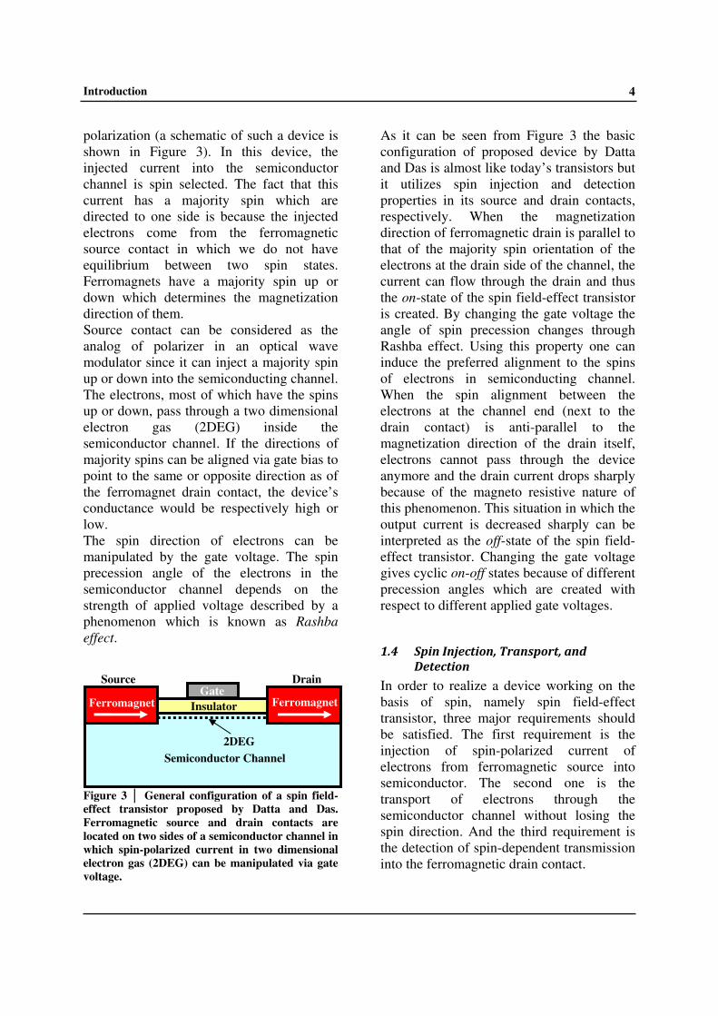
polarization (a schematic of such a device is
shown in Figure 3). In this device, the
injected current into the semiconductor
channel is spin selected. The fact that this
current has a majority spin which are
directed to one side is because the injected
electrons come from the ferromagnetic
source contact in which we do not have
equilibrium between two spin states.
Ferromagnets have a majority spin up or
down which determines the magnetization
direction of them.
Source contact can be considered as the
analog of polarizer in an optical wave
modulator since it can inject a majority spin
up or down into the semiconducting channel.
The electrons, most of which have the spins
up or down, pass through a two dimensional
electron gas (2DEG) inside the
semiconductor channel. If the directions of
majority spins can be aligned via gate bias to
point to the same or opposite direction as of
the ferromagnet drain contact, the device’s
conductance would be respectively high or
low.
The spin direction of electrons can be
manipulated by the gate voltage. The spin
precession angle of the electrons in the
semiconductor channel depends on the
strength of applied voltage described by a
phenomenon which is known as Rashba
effect.
Figure 3 │ General configuration of a spin field-
effect transistor proposed by Datta and Das.
Ferromagnetic source and drain contacts are
located on two sides of a semiconductor channel in
which spin-polarized current in two dimensional
electron gas (2DEG) can be manipulated via gate
voltage.
As it can be seen from Figure 3 the basic
configuration of proposed device by Datta
and Das is almost like today’s transistors but
it utilizes spin injection and detection
properties in its source and drain contacts,
respectively. When the magnetization
direction of ferromagnetic drain is parallel to
that of the majority spin orientation of the
electrons at the drain side of the channel, the
current can flow through the drain and thus
the on-state of the spin field-effect transistor
is created. By changing the gate voltage the
angle of spin precession changes through
Rashba effect. Using this property one can
induce the preferred alignment to the spins
of electrons in semiconducting channel.
When the spin alignment between the
electrons at the channel end (next to the
drain contact) is anti-parallel to the
magnetization direction of the drain itself,
electrons cannot pass through the device
anymore and the drain current drops sharply
because of the magneto resistive nature of
this phenomenon. This situation in which the
output current is decreased sharply can be
interpreted as the off-state of the spin field-
effect transistor. Changing the gate voltage
gives cyclic on-off states because of different
precession angles which are created with
respect to different applied gate voltages.
1.4 Spin Injection, Transport, and
Detection
In order to realize a device working on the
basis of spin, namely spin field-effect
transistor, three major requirements should
be satisfied. The first requirement is the
injection of spin-polarized current of
electrons from ferromagnetic source into
semiconductor. The second one is the
transport of electrons through the
semiconductor channel without losing the
spin direction. And the third requirement is
the detection of spin-dependent transmission
into the ferromagnetic drain contact.
Semiconductor Channel
Ferromagnet Insulator
Source Drain Gate
2DEG
Ferromagnet

Introduction
5
Even overcoming the first requirement is by
itself a big challenge and it is not so
straightforward to inject spin-polarized
current into semiconductor by making a
contact between a ferromagnetic metal and a
semiconductor. A ferromagnetic metal
contains an excess of electrons whose spins
are directed to one side that forms the
magnetization direction of the ferromagnet.
One may expect that these imbalanced spin-
polarized electrons can be injected into the
semiconductor by applying a voltage to the
ferromagnet metal-semiconductor contact.
But in reality spin-polarized electrons cannot
be injected from ferromagnetic metal into
semiconductor in this way. This arises from
the fact that conduction of ferromagnetic
metal is by far bigger than that of
semiconductor and any voltage applied to
the ferromagnetic metal-semiconductor
contact falls on the edges of semiconductor.
Since the origin of this problem arises from
the fact that conductance of different layers
in the contact are different, this problem is
known as conductivity mismatch [7]. In
order to overcome this problem one can
introduce a thin layer of insulator at the
boundary between the ferromagnetic metal
and semiconductor. This barrier provides a
spin-dependent tunnel resistance that allows
the spin injection into the semiconductor.
Figure 4 │ A schematic representation of spin
field-effect transistor consisting of a ferromagnetic
source, a Semiconductor channel, and a
ferromagnetic drain. An insulator is incorporated
between different contacts and semiconductor
channel. Cyan arrows show possible routs of
electrons.
A schematic representation of different
contacts to the semiconductor along with
direction of spin-polarized current in spin
field-effect transistor is shown in Figure 4.
Arrow number (1) in this figure shows the
direction of successfully injected spin-
polarized electrons from ferromagnetic
source contact into semiconductor channel
through tunneling.
Meeting the second requirement that was
mentioned in the beginning of this section
(which deals with transport inside
semiconductor channel) necessitates the
transport of electrons in the channel while
their spin direction is maintained (arrow
number (2) in Figure 4 shows the spin-
polarized current inside the semiconductor
channel). If spin-polarized current moves
through the semiconductor in a diffusive
transport regime (in this kind of transport,
electrons scatter continuously on their way
through the lattice), we expect electrons to
lose their spin direction after a short distance.
This happens because of the fact that after
each scattering it is more likely that
electrons adopt a new spin direction and lose
their original spin direction. In order to
maintain the spin direction, electrons should
travel through the semiconductor in a
ballistic transport regime (in this kind of
transport, electrons move inside the channel
without any scatterings). This means that
electrons should have the minimum number
of scatterings as possible while moving from
the source contact to the drain contact.
The rules governing the spin-dependent
transmission (third condition) are almost the
same as rules applied to spin-dependent
injection that was explained earlier. Those
common rules include the conductivity
mismatch problem which should be
addressed here again. Besides, in order to
have a good output signal, one should raise
the probability by which the spins are going
from semiconductor channel into the
ferromagnetic drain contact (arrow number
Semiconductor
Channel
Insulator
Gate Drain
Ferro-
magnet
Source
Insulator
(1) (2) (3) (4)
Ferro-
magnet

Introduction
6
(3) in Figure 4). Otherwise, back scattered
electrons (arrow number (4)) are more likely
to lose their spin property and decrease the
spin-up, spin-down ratio when electrons try
again to pass through the barrier towards the
ferromagnetic drain contact.

Spin Field Effect Transistor: Concepts from a Device Point of View
7
2 Spin Field-Effect Transistor: Concepts from a Device Point of View
2.1 Benefits of Utilizing Spin Field-Effect
Transistor
It is now several decades that human effort
has been focused on optimizing the size,
speed, and power consumption of existing
metal-oxide-semiconductor field-effect
transistors (MOSFETs) or the so called
charge based transistors. But why after all
the progresses made in the field of charge
based transistors, we are now pursuing to
improve devices which work on the basis of
spin transfer technology?
The first answer to this question can be
discussed from an energy point of view
when transistors are working in dynamic
(active) mode. In order to continue
marvelous progress in improving the device
performance, the predicted switching energy
(energy which is needed to switch between
on and off states) by international
technology roadmap for semiconductors in
2018 is 1500 eV/µm [8]. The switching
energy required for devices which work on
the basis of charge transfer even for an
imaginary gate width of 10 nm (the smallest
gate width reached so far is about 40 nm),
would be approximately three orders of
magnitude larger than this amount [9]. On
the other hand, the minimum switching
energy for the spin field-effect transistor that
Datta and Das proposed is only 23 meV [10].
These numbers show a huge advantage of
spin based transistors over present charge
based devices.
The second reasoning is again from an
energy point of view but this time for a
situation in which transistors are working in
their static mode (this time they are not
switched between on and off states but they
have to keep their on-off states). In spin
based transistors the static power dissipation
is reduced to zero due to their magnetic
nature of data storage, while in present
charge based devices the static power
dissipation is a major challenge in improving
transistor performance. Static power
dissipation in charge based devices is due to
source drain leakage and can be minimized
by increasing the barrier (for example by
increasing channel length). However, we
now that this solution which aims at
decreasing the static power dissipation, at
the same time increases the dynamic power
consumption of the device. This happens
because when there is a higher barrier in the
device, there should be a higher voltage
applied to the contacts of the device that
leads to higher power consumption.
In addition, spin based transistors can further
down scale the transistor devices while the
charge based devices already have reached
their minimum limit of gate length which is
approximately 40 nm. This gives the third
reason to the question made in the beginning
of this section.
In order to better compare spin transfer
devices with its currently mature charge
transfer rival, here we explain the
fundamental differences between the two
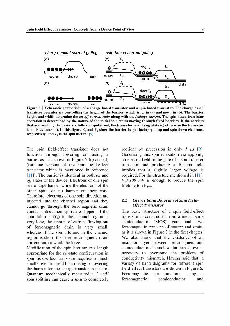
devices in Figure 5. The left side of this
figure shows the operation mechanism of a
charge based transistor. In part (a) of the
Figure 5 a barrier is raised to turn the drain
current off while in part (b) of the Figure 5
this barrier is removed to have the current
flowing to drain. Barrier has to be
sufficiently high and thick to maintain a
large on-off ratio for the drain current. A
problem which arises in this kind of devices
stems from the fact that the higher and
thicker this barrier is the larger the threshold
voltage, and thus, the larger the gate
switching energy will be.
Spin Field Effect Transistor: Concepts from a Device Point of View
8
Figure 5 │ Schematic comparison of a charge based transistor and a spin based transistor. The charge based
transistor operates via controlling the height of the barrier, which is up in (a) and down in (b). The barrier
height and width determine the on-off current ratio along with the leakage current. The spin based transistor
operation is determined by the nature of the initial spin states moving through fixed barriers. If the carriers
that are reaching the drain are fully spin-polarized, the transistor is in its off state (c) otherwise the transistor
is in its on state (d). In this figure E↑ and E↓ show the barrier height facing spin-up and spin-down electrons,
respectively, and T1 is the spin lifetime [9].
The spin field-effect transistor does not
function through lowering or raising a
barrier as it is shown in Figure 5 (c) and (d)
(for one version of the spin field-effect
transistor which is mentioned in reference
[11]). The barrier is identical in both on and
off states of the device. Electrons of one spin
see a large barrier while the electrons of the
other spin see no barrier on their way.
Therefore, electrons of one spin direction are
injected into the channel region and they
cannot go through the ferromagnetic drain
contact unless their spins are flipped. If the
spin lifetime (T1) in the channel region is
very long, the amount of current flowing out
of ferromagnetic drain is very small,
whereas if the spin lifetime in the channel
region is short, then the ferromagnetic drain
current output would be large.
Modification of the spin lifetime to a length
appropriate for the on-state configuration in
spin field-effect transistor requires a much
smaller electric field than raising or lowering
the barrier for the charge transfer transistor.
Quantum mechanically measured a 1 meV
spin splitting can cause a spin to completely
reorient by precession in only 1 ps [9].
Generating this spin relaxation via applying
an electric field to the gate of a spin transfer
transistor and producing a Rashba field
implies that a slightly larger voltage is
required. For the structure mentioned in [11],
Vth≈100 mV is enough to reduce the spin
lifetime to 10 ps.
2.2 Energy Band Diagram of Spin Field-
Effect Transistor
The basic structure of a spin field-effect
transistor is constructed from a metal oxide
semiconductor (MOS) gate and two
ferromagnetic contacts of source and drain,
as it is shown in Figure 3 in the first chapter.
We also know that the existence of an
insulator layer between ferromagnets and
semiconductor channel so far has shown a
necessity to overcome the problem of
conductivity mismatch. Having said that, a
variety of band diagrams for different spin
field-effect transistors are shown in Figure 6.
Ferromagnetic p-n junctions using a
ferromagnetic semiconductor and

Spin Field Effect Transistor: Concepts from a Device Point of View
9
ferromagnetic Schottky junctions using a
ferromagnetic metal all can be employed as
the source or drain of spin field-effect
transistors. The on-off operation states of the
spin field-effect transistor are based on the
modification induced through the gate
voltage by which the height or width of the
barrier structure at the source-channel
junction is slightly changed. Examples of
these kinds of junctions are shown in Figure
6 (a) and Figure 6 (b). Here, the
ferromagnetic source and drain act as spin
injector and spin detector, respectively, and
therefore the output current depends on the
magnetization configurations of the source
and drain and also on spin relaxation length
(an average distance up to which electrons
keep their spin directions intact).
Half-metallic ferromagnets are also useful
for the ferromagnetic source and drain. The
band structure of half-metallic ferromagnets
is comprised of metallic and insulating or
semiconducting spin bands and thus half-
metallic ferromagnets show one hundred
percent spin-polarization at the Fermi energy
[12]. The spin band of metallic part of half-
metallic ferromagnet contacts forms a
Schottky junction with the semiconductor
channel, and the spin band of insulating part
forms an energy barrier that its barrier height
is proportional to the band gap of the
insulating spin band. Thus, the spin-
dependent barrier structure appears at the
source and drain junctions as it is shown in
Figure 6 (c). Another way to realize spin
field-effect transistor is to employ tunnel
junctions for the ferromagnetic source and
drain [13]. So far different kinds of
ferromagnetic semiconductors,
ferromagnetic metals, and half-metallic
ferromagnets have been used for the
ferromagnetic electrodes of the tunnel
junctions.
Figure 6 │ Band diagrams of spin field-effect transistor with (a) ferromagnetic semiconductor source/drain,
(b) ferromagnetic metal source/drain, (c) half-metallic ferromagnet source/drain, and (d) ferromagnetic
tunnel contact source/drain [12].

Spin Field Effect Transistor: Concepts from a Device Point of View
10
When a metallic ferromagnet or a half-
metallic ferromagnet is used for the
ferromagnetic electrodes of the source or
drain, the energy difference between the
Fermi energy of the metallic or half-metallic
ferromagnet and the conduction band edge
of the channel act as an effective Schottky
barrier ( SB
effϕ shown in Figure 6 (d)).
Therefore, control of the effective Schottky
barrier height instead of tunnel barrier height
or thickness is very essential even for the
tunnel junction contacts in order to tune the
junction contact resistance. A spin field-
effect transistor can also be comprised of a
metal oxide semiconductor gate with a
ferromagnetic semiconductor channel and
ferromagnetic Schottky junctions for both
the source and drain [14].
2.3 Device Structures of Spin Field-Effect
Transistor
Ferromagnetic metals are the best candidates
for making room temperature spin field-
effect transistor source and drain contacts.
However, as it was discussed earlier,
conductivity mismatch between
ferromagnetic metal contacts for source and
drain hampers the spin injection into the
channel and spin detection in drain. When
we are dealing with diffusive electron
transport in the channel, the much lower
resistivity of the ferromagnetic metal in
source or drain compared to that of the
channel causes the almost same drop of the
electrochemical potentials over the channel
for both spin-up and spin-down electrons
which cannot ensure efficient spin injection.
Therefore, spin-dependent interfacial contact
resistance (at the source or drain junctions)
which is sufficiently larger than the channel
resistance is required for efficient spin
injection [15]. This increase in interfacial
contact resistance decreases the overall
device performance as it lowers the total
conductance of the transistor device. Since
the channel resistance in the on-state can be
reduced with decreasing the channel length,
the spin-dependent contact resistance should
also be reduced with decreasing the channel
length. Schottky junctions that use very thin
low work function interfacial layers are
promising junctions [16] since they can be
further down scaled while still maintaining
contact resistance character necessary for
spin-dependent current injection.
Conductivity mismatch problem in the
ballistic transport regime is considered to be
non-relevant, because the resistance of the
channel can be assumed zero. But we know
that there is a large contact resistance at the
source and drain junctions in the ballistic
transport regime. This contact resistance
deals with the output current and not that of
the channel resistance, and hence the
conductivity mismatch problem exists even
in the ballistic regime [17]. Therefore, spin-
dependent contact resistance is required for
both diffusive transport and ballistic
transport regimes. Since the resistivity of the
ferromagnets is comparable to that of the
channel, it rules out conductivity mismatch
problem [12] and therefore ferromagnetic
semiconductors are attractive candidates for
source and drain materials. Other possible
candidates may are half-metallic
ferromagnet contacts with the spin-
polarization of 100 % [12] for the source and
drain contacts. Although in this case the
tuning of the contact resistance would not be
needed, the reduction of the Schottky barrier
height is still required in order to have a
good device performance.
Two device structures for spin field-effect
transistors are shown in Figure 7. We call
these structures bulk spin field-effect
transistor and silicon on insulator (SOI) spin
field-effect transistor corresponding with
their configurations. Low production cost for
bulk spin field-effect transistors and

Spin Field Effect Transistor: Concepts from a Device Point of View
11
excellent device performance for SOI spin
field-effect transistors is expected [12]. In
the bulk spin field-effect transistor, the
ferromagnetic source or drain act as
electrical contacts to the channel when the
transistor is working in its on-state, and they
work as blocking contacts for leakage
current between the source and drain when
the transistor is in its off-state.
Figure 7 │ Possible device structures of (a) bulk
spin field-effect transistor and (b) Silicon on
insulator (SOI) spin field-effect transistor [12].
Again considering the problem of
conductivity mismatch, we see that p-n
junctions which use a ferromagnetic
semiconductor are the most suitable
structures for the ferromagnetic source and
drain configurations. On the other hand,
Schottky junctions that use a ferromagnetic
metal are also applicable to the
ferromagnetic source or drain structures. We
should note that in the bulk spin field-effect
transistor, relatively high junction leakage
current would be problematic for the
Schottky junction contacts. Since the SOI
spin field-effect transistor structure
considerably minimize the junction area of
the source and drain, this device structure is
preferable for Schottky junction contacts.
The dopant segregation effect during the
formation of ferromagnetic silicides and the
auto doping effect of epitaxial ferromagnetic
metals which are grown on Si [18] are also
effective to a large extent in reducing the
junction leakage current of the ferromagnetic
metal source and drain even in the bulk spin
field-effect transistor structures.
One possible device structure of a spin field-
effect transistor using nonmagnetic p-n
junctions for the source and drain, where
ferromagnetic metal or half-metallic
ferromagnet contacts are formed on or inside
the source and drain regions is shown in
Figure 7 (a) (in this figure n+ means highly
n-doped). Tunnel contacts due to the
Schottky junctions between the
ferromagnetic metal and n+ region can be
used to remove the conductivity mismatch
problem. Work function engineering using
both an ultrathin interfacial insulating layer
and an ultrathin low work function metal
layer deposited on it to control the Schottky
barrier height [16] is more likely to achieve
the ferromagnetic contacts of source and
drain. Since, SiO2, Si3N4, and Al2O3 induce
only a small density of interface states [12],
these materials are promising candidates for
interfacial insulating layers. Other
prospective materials for the realization of
an efficient, high spin injection rate are
CoFe/MgO, CoFeB/MgO, and Heusler-
alloy/MgO with a low work-function metal
layer [12] placed at interfacial barrier to
control barrier height.
Another possible device structure of a spin
field-effect transistor which uses a thin
semiconductor on insulator (SOI) structure is
schematically shown in Figure 7 (b). The p-n
junction based on ferromagnetic source or
drain structures shown in Figure 7 (a) can be
also applied to the SOI spin field-effect
transistor structure while ferromagnetic
Schottky junctions are themselves an
alternative candidate. The thin body SOI
Spin Field Effect Transistor: Concepts from a Device Point of View
12
spin field-effect transistor structure provides
several adjustable options in order to
improve the device performance. In this
configuration even when the ferromagnetic
source and drain are in the form of Schottky
junctions, the junction leakage current can
be considerably reduced due to the
extremely small junction area. Furthermore,
a lower degree of doping for the channel or
an intrinsic channel can be used in this
device structure, which plays an essential
role to exclude or minimize scattering of
spin-polarized electrons that are transported
through the channel. These characteristics
show that in short SOI channels the ballistic
transport of spin-polarized electrons can be
expected.
To tune the contact resistance, silicidation
reaction can be used to form the
ferromagnetic source and drain [19]. In other
words the dopant segregation effect during
the silicidation in this case is helpful. The
other promising way to control the contact
resistance is to create Schottky junctions
using low work function materials which are
placed next to interfacial insulating layer.

Some Recent Advances in Spin Injection, Transport, and Detection
13
3 Some Recent Advances in Spin Injection, Transport, and Detection
3.1 Spin Injection into Silicon
One of the successful works on injecting
spin-polarized electrons from a ferromagnet
into the silicon channel has been done by B.
T. Jonker et al. [20]. They could successfully
inject spin-polarized current from a
ferromagnetic iron film through an Al2O3
tunnel barrier into Si (001) n-i-p doped
hetero-structure.
Figure 8 │ (a, and b) When electrons are injected
from the Fe contact under electrical bias, radiative
recombination is observed as the electrons
recombine with unpolarized holes in either the Si
(n-i-p structure) (a) or the GaAs quantum well,
Si/AlGaAs/GaAs/AlGaAs structure (b). (c) Band
diagram showing the exchange split bands of the
Fe contact, with majority spin electron states
highlighted in red (up arrow) and minority spin
states highlighted in blue (down arrow). (d)
Photograph of processed light emitting diode
(LED) structures. The circular plates are the
active light emitting areas, the contact
metallization appears in yellow and the wire
contacts appear to the right [20].
The circular polarization of the
electroluminescence resulting from radiative
recombination in Si and GaAs structures was
a signature of the existence of spin-
polarization current in semiconductor
originating from Fe magnetization.
They determined a 30% difference between
majority and minority spins before radiative
recombination with unpolarized holes in Si
happens at 5 K. they observed the difference
in majority and minority spin-polarization at
temperatures of up to 125 K. These results
were confirmed by repeating the same
experiments on Fe/Al2O3/Si/AlGaAs/GaAs
quantum well structures in which the spin-
polarized electrons flow under applied field
from the Si, and recombine later in the GaAs
quantum well, where the polarized
electroluminescence can be quantitatively
analyzed (the schematic representation of
these two structures are shown in Figure 8).
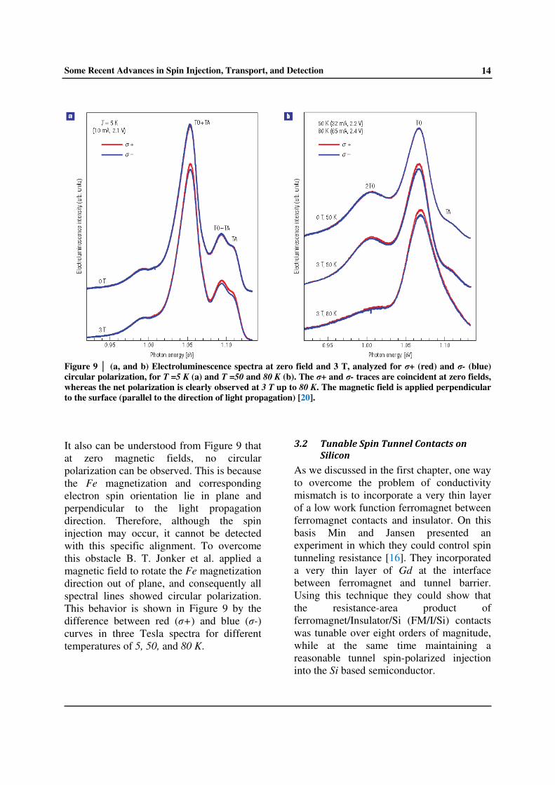
In Figure 9 electroluminescence spectra
from a Fe/Al2O3/Si n–i–p structure are
shown for 5, 50, and 80 K. these
electroluminescence data are analyzed for
both σ+ (right handed) and σ- (left handed)
circular polarizations. At 5 K, three peaks
can be seen which arise from electron hole
recombination accompanied by transverse
acoustic (TA) or transverse optical (TO)
phonon emission in the p-doped Si layers.
These peaks are detected at 1.105 meV
associated with transverse acoustic, 1.09
meV associated with TO-TA, and finally
1.05 meV associated with TO+TA. At higher
temperatures transverse acoustic related
features are diminished as it can be seen in
Figure 9 (b). Here we can see that the
transverse optical feature occurring at 1.07
meV dominates both temperatures of 50 and
80 K.
Some Recent Advances in Spin Injection, Transport, and Detection
14
Figure 9 │ (a, and b) Electroluminescence spectra at zero field and 3 T, analyzed for σ+ (red) and σ- (blue)
circular polarization, for T =5 K (a) and T =50 and 80 K (b). The σ+ and σ- traces are coincident at zero fields,
whereas the net polarization is clearly observed at 3 T up to 80 K. The magnetic field is applied perpendicular
to the surface (parallel to the direction of light propagation) [20].
It also can be understood from Figure 9 that
at zero magnetic fields, no circular
polarization can be observed. This is because
the Fe magnetization and corresponding
electron spin orientation lie in plane and
perpendicular to the light propagation
direction. Therefore, although the spin
injection may occur, it cannot be detected
with this specific alignment. To overcome
this obstacle B. T. Jonker et al. applied a
magnetic field to rotate the Fe magnetization
direction out of plane, and consequently all
spectral lines showed circular polarization.
This behavior is shown in Figure 9 by the
difference between red (σ+) and blue (σ-)
curves in three Tesla spectra for different
temperatures of 5, 50, and 80 K.
3.2 Tunable Spin Tunnel Contacts on
Silicon
As we discussed in the first chapter, one way
to overcome the problem of conductivity
mismatch is to incorporate a very thin layer
of a low work function ferromagnet between
ferromagnet contacts and insulator. On this
basis Min and Jansen presented an
experiment in which they could control spin
tunneling resistance [16]. They incorporated
a very thin layer of Gd at the interface
between ferromagnet and tunnel barrier.
Using this technique they could show that
the resistance-area product of
ferromagnet/Insulator/Si (FM/I/Si) contacts
was tunable over eight orders of magnitude,
while at the same time maintaining a
reasonable tunnel spin-polarized injection
into the Si based semiconductor.

Some Recent Advances in Spin Injection, Transport, and Detection
15
Figure 10 │ (a) Cross-sectional transmission electron micrograph of Si/Al2O3/Co contacts. (b) Resistance-area
product of the tunnel contact at the reverse bias of +0.2 V versus the thickness of the Al2O3 tunnel barrier.
The red data is for the Si/Al2O3/Co (Ni80Fe20) (15nm) contacts, the blue data is for the Si/Al2O3s/Gd (15 nm)
contacts. (c) Absolute value of current density versus bias voltage of Si/Al2O3 (0.5nm)/Ni80Fe20 (15 nm),
Si/Al2O3 (0.5nm)/Gd (15 nm) and Si/Al2O3 (0.5nm)/Gd (0.3–5 nm)/Ni80Fe20 contacts. The minus voltage is the
forward bias (the spin detection condition); the positive voltage is the reverse bias (the spin injection
condition). (d) Resistance-area product of the Si/Al2O3 (0.5nm)/Gd/Ni80Fe20 (10 nm) contacts at a reverse bias
of +0.2 V versus the thickness of the Gd interlayer. The inset shows the Schottky barrier height of the contact
versus the thickness of the Gd interlayer. The error bars denote the accuracy of the determination of the Gd
thickness [16].
The Schottky barrier height of a FM/I/Si
contact is determined by the work function
of the metal, the electron affinity of Si and
the number of surface states at the Si surface
[21]. The Schottky barrier height can be
decreased using a material with a work
function lower than that of Co, Ni, or Fe [22],
while the material should still be
ferromagnetic to have the ability to inject
spin-polarized electrons into the Si channel.
They used Gd as the low work function
ferromagnetic material to control the
resistance-area product of spin tunnel
contacts.
In their experiment ferromagnet-insulator-
semiconductor (FM/I/Si) contacts were
fabricated with well-known ferromagnetic
materials, Co and Ni80Fe20. Figure 10 (a)
shows a cross-sectional transmission
electron micrograph of a Si/Al2O3/Co
Some Recent Advances in Spin Injection, Transport, and Detection
16
contact on low doped n-type Si substrates.
The resistance-area product of the contact is
defined as the voltage, V, divided by the
current density, I/A, at a particular value of V.
The resulting resistance-area product for this
configuration was about eight orders of
magnitude higher than the value needed for
efficient spin injection.
When an ultrathin layer of Gd is used
between ferromagnet and insulator, the
resistance-area product of the Si/Al2O3/Gd
contact reaches the optimum range in Figure
10 (b) for both spin injection and spin
detection contacts. The resistance-area
product of the contact with a Gd layer shows
an exponential dependence on the barrier
thickness as it can be seen in this figure. It
means that the dominant transport
mechanism across the Al2O3 barrier in this
case is the tunnel transport.
Figure 10 (c) shows the I–V characteristics
of a Si/Al2O3(0.5 nm)/Ni80Fe20 and a
Si/Al2O3(0.5nm)/Gd tunnel contact on low
doped Si. As it is shown in this figure, the
current density of the Si/Al2O3/Ni80Fe20
contact is very small in the reverse bias
range and it only has a small dependence on
the voltage. In contrast, the current density
of the Si/Al2O3/Gd tunnel contact in the
reverse bias range is more than seven orders
of magnitude larger than the current density
for Si/Al2O3/Ni80Fe20. We can also see from
this figure that the current density of the
Si/Al2O3/Gd tunnel contact in the forward
bias range is considerably increased.
Therefore, the I–V curves of contacts with
Gd show symmetric behavior, which is
important in obtaining the same resistance-
area product for source and drain contacts.
The resistance area product of the tunnel
contacts decreases suddenly by increasing
the thickness of the Gd interlayer and
saturates to the resistance area product of the
FM/I/Si contact when Gd interlayer is 15 nm.
This situation is shown in Figure 10 (d) and
as it can be seen the resistance-area product
for a 1 nm Gd interlayer, for the case of spin
injection condition (V =+0.2 V), is reduced
by about eight orders of magnitude. Similar
behavior occurs for the resistance area
product in the case of spin detection
(negative bias). When the thickness of the
Gd layer is more than about 1 nm, the
resistance area product of the contact at a
constant value saturates. This is because
when the thickness of Gd is 1 nm, the
surface coverage of the Gd is complete [16]
(we know that the work function is sensitive
to the outermost surface layers of a material).
Also it can be seen that temperature
dependence still remains for the tunnel
contacts with a Gd interlayer thinner than
0.7 nm. At the same time we see that, this
temperature dependence disappears for the
tunnel contacts with a Gd interlayer thicker
than 1.0 nm (for which the Schottky barrier
is removed).
3.3 Spin Transport in GaAs
One of the most remarkable works on
electrical detection of spin transport in
ferromagnetic-semiconductor devices was
done by P. A. Crowell et al. [23] in 2007.
They demonstrated a fully electrical scheme
for achieving spin injection, transport and
detection in a GaAs based device. Since
optical spin detection methods are very
successful in GaAs the electrical
experiments in their work could be verified
by optical means. Their device, as it is
shown in Figure 11, consisted of a main
semiconductor channel with several
ferromagnetic contacts. Considering
different experiments, relevant contacts were
used as source and drain to measure both
local (when the same contacts are used as
voltage application and detection) and non-
local (when different contacts are used as
voltage application and detection) spin-
polarizations of the electrons.

Some Recent Advances in Spin Injection, Transport, and Detection
17
In a non-local spin sensitive current
detection, Schottky tunnel barrier contact’s
electrochemical potential depends on the
relative magnetizations of the source and
drain (drain here is called detector). They
verified the effectiveness of their device
configuration by showing the existence of
Hanle effect (in Hanle effect a transverse
magnetic field suppresses the non-local
signal at the detection contact by inducing
spin precession and dephasing in the
channel). The output signal was varying with
the injection current and was correlated with
the spin-polarization in the channel.
Figure 11 │ (a) A schematic diagram of the non-local experiment configuration. Five 10×50 µm Fe contacts
have their magnetic easy axes along y , which is in [011] direction of the GaAs. The large arrows on Fe
contacts indicate the magnetizations of the source and detector. Length of the two main channels and distance
between Fe contacts are l1 =160 µm and l2 =12 µm, respectively. Electrons are injected along the direction that
is shown in red. The injected spins (purple) diffuse in either direction from contact 3 and the non-local voltage
is detected at contact 4. (b) A non-local voltage, V4,5, versus in-plane magnetic field By which is swept in both
directions at a current of I1,3 =1.0 mA at T=50 K, can be seen. The raw data are shown in the upper panel with
an offset V0=-30.227 mV subtracted. The background here is shown as dashed cyan curve underneath the data
and is fitted by a second order polynomial. The lower shows the data while this background data is subtracted.
(c) Another non-local voltage, V4,5, but this time magnetic field is in the direction of z (Bz) for the same
contacts and bias conditions and the same offset V0 as in part (b). The dashed cyan curve data in the lower
panel again is the upper panel raw data subtracted by background data. The data that are shown in black are
obtained with the magnetizations of contacts 3 and 4 parallel while the data shown in red are obtained in the
anti-parallel configuration [23].

Some Recent Advances in Spin Injection, Transport, and Detection
18
The interpretation of electrical spin-transport
measurements can be complicated by
background effects (background effects
include magneto resistance in the electrodes,
local Hall effects and other extrinsic
contributions to the signal). A non-local
measurement minimizes these background
effects by placing a spin detection electrode
outside the path of the charge current.
Figure 11 (a) shows a schematic diagram of
the non-local experiment configuration that
was used in this experiment. In this figure
the magnetic easy axes of five 10×50 µm Fe
contacts are at y direction (i.e., in [011]
direction of the GaAs). The large arrows on
Fe contacts indicate the magnetizations of
the source and detector. Length of the two
main channels and distance between Fe
contacts are l1 =160 µm and l2 =12 µm,
respectively. Electrons are injected along the
direction that is shown in red. The injected
spins (purple) diffuse in both left and right
directions from contact 3 and the non-local
voltage is detected at contact 4.
The data in Figure 11 (b) indicates the
existence of a lateral spin-valve effect. In
this figure non-local voltage, V4,5, versus in-
plane magnetic field By which is swept in
both directions at a current of I1,3 =1.0 mA at
T=50 K, is presented. The raw data are
shown in the upper panel with an offset V0=-
30.227 mV subtracted. The background here
is shown as dashed cyan curve underneath
the data and is fitted by a second order
polynomial. Lower part of this figure shows
the data while this background data is
subtracted. Two squares jump with a
magnitude of 16.8±0.2 µV and occur in a
field range in which the magnetizations of
contacts 3 and 4 are anti-parallel.
What is most significant in their work is the
fact that previous measurements done by
other research groups on devices having
ferromagnetic-semiconducting contacts, had
not demonstrated precession of the spin on
their way from source to drain. To
investigate this property they used the Hanle
effect [24], in which the magnetic field
dependence of the non-local voltage was due
to precession and dephasing of the spins in
the semiconductor channel. The precession
was induced by applying a small transverse
magnetic field to the extent that it could not
change the magnetizations of the electrodes.
In their experiment they set the
magnetizations of contacts 3 and 4 in
parallel and the external magnetic field in
the direction of Bz. the magnetic field then
swept through the range -400 G to 400 G
resulting in the black data points shown in
the top panel of Figure 11 (c). The offset V0
is the same as for Figure 11 (b). The
corresponding data after subtraction of the
background are shown here as dashed cyan
lines in the lower panel of Figure 11 (c).
This procedure was repeated for anti-parallel
configuration of contacts 3 and 4 which
resulted in the red data points in Figure 11
(c). It can be seen from this figure that the
two Hanle curves coincide at large Bz as in
this limit the electron spins in the GaAs
channel are completely dephased. The
difference in two Hanle signals at B = 0 is
18.0±0.1 µV, which is different from the
jump in the spin-valve data by an amount of
1.2 µV.
3.4 Spin Transport in Silicon
Earlier we discussed how Crowell et al. [23]
could measure and verify the spin transport
across a channel of 160 µm in GaAs. Since
the mainstream industry is based on silicon
technology, it is very important if we can
find a way to transport spin-polarized
electrons across long distances in silicon.
Along with the realization of this goal, I.
Appelbaum et al. [25] conducted a
successful experiment and measured a
controlled spin transport in silicon. They
could transport and measure a spin-polarized
current across 10 µm undoped Si in a

Some Recent Advances in Spin Injection, Transport, and Detection
19
ballistic transport regime. The silicon was
sandwiched between ferromagnetic thin
films for both spin injection and spin
detection. The hot electron (a hot electron is
an electron which is not in thermal
equilibrium with its semiconducting
environment) spin injection and spin
detection that was used in their experiment
avoided resistance mismatch between
ferromagnetic and semiconducting layers. A
schematic representation of this device is
shown if Figure 12.
Figure 12 │ (a) Schematic band diagram. At
constant emitter voltage (Ve), the first collector
current (Ic1) is measured at the NiFe contact and
second collector current (Ic2) is measured at an In
contact to the n-doped Si substrate, under optional
voltage bias (Vc1) across the single crystal undoped
float zone Si (FZ-Si) drift region. (b) A top down
micrograph of a representative wire bonded Si
spin transport device it shows the device structure,
contacts to the tunnel junction base and emitter,
and spin detector buried NiFe layer [25].
In step 1, unpolarized electrons are injected
from Al emitter into the ferromagnetic
Co84Fe16 through tunnel junction and create
emitter current Ie. In step 2, the flow of
minority spin electrons is attenuated through
scattering. In step 3, majority electrons
which have their spins parallel to the
magnetization of Co84Fe16 are transported
over Schottky barrier into float zone (FZ)
and form the first collector current Ic1. In
step 4, the majority spin-polarized current
makes its way through m10 µ undoped Si.
In step 5, second collector current Ic2
(magnitude of Ic2 depends on the relative
magnetization direction of both
ferromagnetic layers) is formed from
ballistic transport through ferromagnetic
Ni80Fe20 into n-doped Si substrate. When
magnetizations of the two ferromagnetic
layers are parallel, Ic2 is higher than when
the magnetizations are anti-parallel.
In Figure 13 in-plane magnetic field
dependence of second collector current (Ic2)
at Ve=-1.8 V and 85 K is shown.
Measurements begin from the far ends of the
figure when the magnetization directions of
two ferromagnets are parallel. When the
magnetic field is swept through zero it
changes sign and first forces the
magnetization of Ni80Fe20 to switch (in the
direction of applied field) so that the
magnetization directions of ferromagnets are
anti-parallel. This results in a reduction in Ic2
of approximately two percent. By further
increasing the magnetic field strength, the
magnetization direction of Co84Fe16 is also
aligned with the applied magnetic field
direction. In this way again higher collector
current (Ic2) is obtained. The symmetric
magnetic field dependence of Ic2 upon
reversal of sweep direction in Figure 13
indicates that the electron spin maintains
polarization while travelling through 10 µm
thick of float zone silicon.

Some Recent Advances in Spin Injection, Transport, and Detection
20
Figure 13│ In-plane magnetic field dependence of
second collector current (Ic2) at constant emitter
bias Ve=-1.8 V and Vc1=0 V, showing an
approximate two percent spin valve effect at 85 K
[25].
Dependence of Ic2 on external magnetic field
which is perpendicular to the film plane
(while Vc1=0 V) is shown in Figure 14 (a).
The measurement begins with the field at -5
kOe, where a small in-plane component
orients the in-plane Ni80Fe20 and Co84Fe16
magnetizations parallel to each other.
Following the red line to the right towards
smaller field values, a peak near -0.7 kOe
and a dip near -0.35 kOe can be seen. Once
the magnetic field is past zero, the small in-
plane component of magnetic field switches
the Ni80Fe20 magnetization which causes an
anti-parallel magnetization direction of
source and drain. By reversing the external
magnetic field scan direction (blue line) a
similar feature is obtained.
If the precession of spin direction in the
external magnetic field is to the extent that
when it arrives at the Ni80Fe20 thin film, it is
parallel to the magnetization direction of this
film, a maximum is observed in the Ic2
current. On the other hand, if the precession
of spin direction in the external magnetic
field is to the extent that at the vicinity of the
magnetic thin film it is oriented anti-parallel
to the magnetization direction of Ni80Fe20
thin film, a minimum is observed in the Ic2.
Figure 14│ (a) Second collector current, Ic2, in
zero applied voltage Vc1. (b and c) Like part (a)
but under an accelerating voltage bias of 0.5 V (b)
and of 1.0 V (c). At higher accelerating voltages,
the spin-polarized electron transport time is
reduced in the increased drift field, so the
precession angle at fixed magnetic field is smaller,
causing an increased precession period and
revealing the presence of precession angles up to
4π. In this experiment magnetic field has been
perpendicular to the direction of spin-polarized
current inside the channel at constant emitter
voltage of Ve=-1.8 V and 85 K [25].
When the electric drift field is increased with
an applied voltage bias, Vc1, the transmission
time is reduced, and the precession angle at
any fixed magnetic field is consequently
reduced. This pushes the maxima and
minima to higher values of perpendicular
magnetic fields. These behaviors are shown
in Figure 14 (b) and (c) for Vc1=0.5 V and
Vc1=1 V accelerating voltages, respectively.
Under these higher accelerating electric
fields, drift is even more dominant than in
Figure 14 (a) and precession angles up to 4π
can be seen.

Conclusion
21
4 Conclusion
If realized, the spin field-effect transistor
will provide many benefits as being smaller,
quicker, using lower power, and generating
lower heat than the present charge based
transistors. However, in order to reach the
point in which spin field-effect transistor is
fully operational, there are some challenges
which need to be overcome. We can
categorize all these challenges into four
main classes, viz. spin injection, spin
transport, spin detection, and spin
manipulation.
We have seen how various research groups
have successfully overcome problems of
conductivity mismatch between
ferromagnets and semiconductors using
different approaches. We have also seen how
some of these groups have addressed issues
regarding spin diffusion time and spin
diffusion length of electrons in the
semiconductor channel. Based on what we
have seen in this article we now know that
challenges like spin injection, spin transport,
and spin detection in semiconductors all
have been successfully addressed and
overcome by different groups.
Nevertheless, these achievements does not
mean that all the problems on the way of
making spin field-effect transistor have been
solved. This would become more obvious
when we look more closely into the recent
works which were described in the last
chapter. Most of the experiments described,
operate in very low temperatures making it
an open challenge to realize room
temperature injection of spins in
semiconductors. And as we know one of the
main objectives in the field of Spintronics is
to make room temperature spin field-effect
transistor devices. Another problem which
can be seen in the most promising three
terminal device made by Appelbaum et. al.
is that it has low output current thus making
the detection of spin-polarized current
difficult at the drain contact. The other
problem on the way of making spin field-
effect transistor arises from the combination
of ferromagnetic materials with
semiconductors which gives rise to many
different compatibility problems. The
mentioned problems might still not be the
most significant ones on the way of
realization of the spin field-effect transistor,
but the most significant challenge might be
to introduce the gate contact by which spins
inside the semiconductor channel can be
manipulated.
In this article we have followed the
progressive trend towards the realization of
spin field-effect transistor after it was first
proposed by Datta and Das almost two
decades ago. Now we come back to the
question that was raised at the beginning of
this article. Can the spin field-effect
transistor be realized? The answer to this
question is yes. Despite various problems on
the way of the spin field-effect transistor
realization, significant achievements by
various groups in especially the last two
years gives hope that the realization of the
spin field-effect transistor, though
challenging can be within reach.
5 Acknowledgments
In the end I want to express my sincere
gratitude to both Caspar van der Wal and
Tamalika Banerjee from Zernike Institute for
Advanced Materials whose kind
consultations led me through all difficulties
while writing this article.

References
22
6 References
1 M. N. Baibich, J. M. Broto, A. Fert et al., "Giant
Magnetoresistance of (001)Fe/(001)Cr Magnetic
Superlattices," Physical Review Letters 61,
2472-2475, (1988).
2 G. Binasch, P. Grunberg, F. Saurenbach et al.,
"Enhanced Magnetoresistance in Layered
Magnetic-Structures with Antiferromagnetic
Interlayer Exchange," Physical Review B 39,
4828-4830, (1989).
3 J. Daughton, J. Brown, E. Chen, R. Beech, A.
Pohm, and W. Kude, “Magnetic field sensors
using GMR multilayer,” IEEE Trans. Magn., vol.
30, no. 6, 4608-4610, (1994).
4 S. Datta and B. Das, "Electronic analog of the
electro-optic modulator," Appl. Phys. Lett. vol.
56, 665-667, (1990).
5 J. S. Moodera, L. R. Kinder, T. M. Wong, and R.
Meservey, “Large magnetoresistance at room
temperature in ferromagnetic thin film tunnel
junctions,” Phys. Rev. Lett. vol. 74, no. 16,
3273–3276, (1995).
6 W. H. Meiklejohn and C. P. Bean, “New
magnetic anisotropy,” Phys. Rev. vol. 102, no. 5,
1413-1414, (1956).
7 G. Schmidt, D. Ferrand, L. W. Molenkamp et al.,
"Fundamental obstacle for electrical spin
injection from a ferromagnetic metal into a
diffusive semiconductor," Physical Review B
vol. 62, R4790-R4793, (2000).
8 International Technology Roadmap for
Semiconductors. Semicond. Ind. Assoc., San
Jose, CA. [Online: http://www.itrs.net/Links
/2003ITRS/PIDS2003.pdf], (2003).
9 M. E. Flatte, “Spintronics,” IEEE Transactions
on Electron Devices vol. 54, no. 5, 907-920,
(2007)
10 R. Landauer, “Irreversibility and heat generation
in the computing process,” IBM J. Res. Develop.
vol. 5, no. 3, 183-191, (1961).
11 K. Hall, W. H. Lau, K. Gundogdu, M. E. Flatte,
and T. F. Boggess, “Nonmagnetic
semiconductor spin transistor,” Appl. Phys. Lett.
vol. 83, no. 14, 2937-2939, (2003).
12 S. Sugahara, “Perspective on field-effect spin-
transistors,” phys. stat. sol. no. 12, 4405-4413,
(2006).
13 S. Sugahara and M. Tanaka, “Spin MOSFETs as
a basis for spintronics,” ACM Transactions on
Storage no. 2, 197, (2006).
14 S. Sugahara and M. Tanaka, “A spin metal-
oxide-semiconductor field-effect transistor (spin
MOSFET) with a ferromagnetic semiconductor
for the channel,” J. Appl. Phys. vol. 97, 10D503,
(2005).
15 A. Fert and H. Jaffres, “Conditions for efficient
spin injection from a ferromagnetic metal into a
semiconductor,” Phys. Rev. B vol. 64, 184420,
(2001).
16 B. C. Min, and R. Jansen et al., “Tunable spin-
tunnel contacts to silicon using low-work-
function ferromagnets,” Nature Materials vol. 5,
817-822, (2006).
17 V. Y. Kravchenko and E.I. Rashba, “Spin
injection into a ballistic semiconductor
microstructure,” Phys. Rev. B vol. 67, 121310,
(2003).
18 K. Sugiura, R. Nakane, S. Sugahara, and M.
Tanaka, “Schottky barrier height of
ferromagnet/Si(001) junctions,” Appl. Phys.
Lett. vol. 89, 072110, (2006).
19 R. Nakane, M. Tanaka, and S. Sugahara,
“Preparation and characterization of
ferromagnetic DO3-phase Fe3Si thin films on
silicon-on-insulator substrates for Si-based spin-
electronic device applications,” Appl. Phys. Lett.
vol. 89, 192503, (2006).
20 G. Kioseoglou, A. T. Hanbicki, C. H. Li, P. E.
Thompson, B. T. Jonker, “Electrical spin-
injection into silicon from a ferromagnetic
metal/tunnel barrier contact,” Nature Physics vol.
3, 542-546, (2007).
21 S. M. Sze, Physics of Semiconductor Devices
2nd edition, Wiley, New York, (1981).
22 D. Connelly, C. Faulkner, P. A. Clifton, and D.
E. Grupp, “Fermi-level depinning for low-
barrier Schottky source/drain transistors,” Appl.
Phys. Lett. vol. 88, 12105, (2006).
23 P. A. Crowell, X. Lou et al., “lateral
ferromagnet-semiconductor devices,” nature
physics vol. 3, 195-202, ( 2007).
24 F. J. Jedema, H. B. Heersche, A. T. Filip, J. J. A.
Baselmans, and B. J. van Wees, “Electrical
detection of spin precession in a metallic
mesoscopic spin valve,” Nature vol. 416, 713-
716, (2002).
25 I. Appelbaum, B. Huang, D. J. Monsma,
“Electronic measurement and control of spin
transport in silicon,” Nature vol. 447, 295-298,
(2007).


![Spin jam induced by quantum fluctuations in a …by quantum fluctuations, a spin jam, that is realized in SrCr 9 pGa 12-9 O 19 [SCGO(p)], a highly frustrated magnet, in which the magnetic](https://img.pdfslide.net/doc/110x75/5f3b2805ff945a43f8777869/spin-jam-induced-by-quantum-fluctuations-in-a-by-quantum-fluctuations-a-spin-jam.jpg)


![The spin-valve transistor: a review and outlookspea2014.chania.teicrete.gr/wp-content/uploads/2014/06/... · 2014-06-20 · semiconductor [16–20], but implementation into working](https://img.pdfslide.net/doc/110x75/5e8d4ebe9e654555f82ac76c/the-spin-valve-transistor-a-review-and-2014-06-20-semiconductor-16a20-but.jpg)