Embed Size (px)
Citation preview
THE TEST AND DIAGNOSIS OFFPGAS
A DISSERTATION
SUBMITTED TO THE DEPARTMENT OF ELECTRICAL ENGINEERING
AND THE COMMITTEE ON GRADUATE STUDIES
OF STANFORD UNIVERSITY
IN PARTIAL FULFILLMENT OF THE REQUIREMENTS
FOR THE DEGREE OF
DOCTOR OF PHILOSOPHY
Erik Chmelar
June 2004

c© Copyright by Erik Chmelar 2004
All Rights Reserved
ii

I certify that I have read this dissertation and that, in my opinion, it
is fully adequate in scope and quality as a dissertation for the degree
of Doctor of Philosophy.
Edward J. McCluskey(Principal Adviser)
I certify that I have read this dissertation and that, in my opinion, it
is fully adequate in scope and quality as a dissertation for the degree
of Doctor of Philosophy.
Giovanni De Micheli
I certify that I have read this dissertation and that, in my opinion, it
is fully adequate in scope and quality as a dissertation for the degree
of Doctor of Philosophy.
Nirmal Saxena
Approved for the University Committee on Graduate Studies.
iii

This page intentionally left blank.
iv
Abstract
A Field-programmable Gate Array(FPGA) is a configurable integrated circuit that can
implement an arbitrary logic design, useful for a wide rangeof applications. However,
because integrated circuit manufacturing is imperfect, defects occur. To cope withdefects,
which cause an FPGA to function incorrectly, the manufacturer must execute two essential
tasks: (1) thorough test to ensure high device quality, and (2) efficient diagnosis to achieve
high manufacturing yield. Because up to 80% of the die area and up to 8 metal layers of an
FPGA constitute the interconnection network, it is the primary focus in both tasks.
The purpose of test is to detect defects. Specialtest configurations, each a mapping
of a logic design to the FPGA hardware, are required to test anFPGA. Because there are
literally billions of possible logic designs and mappings for an FPGA, a trade-off must be
made between test time, which is proportional to the number of test configurations used to
test the device, and defect coverage, which quantifies the types and number of defects that
can be detected. In this dissertation three new test techniques are presented, one to detect
delay faults, one to detect bridge faults, and one to reduce test time.
First, a delay fault test technique is presented that can detect very small delay faults
(nanosecond range) with slowAutomated Test Equipment(ATE) [Chmelar 2003]. A delay
fault, which causes timing failures in an FPGA, is difficult to detect due to the slow test
speeds of contemporary ATE. In the presented technique the logic blocks of an FPGA are
configured intoIterative Logic Arrays(ILAs) to (1) create controlled signal races, and (2)
observe the relative transition times of the racing signalsto detect any delay faults.
Second, a bridge fault test technique is presented that can detect bridge faults more
effectively than standardIDDQ and Boolean tests. Abridge fault, which can create a fault
current, may be detected by measuring the steady-state device current,IDDQ; however,
observing a fault current has become difficult due to both theexponential increase inIDDQ
(resulting from smaller process geometries and lower threshold voltages) and the increase
in the number of transistors per device. The presented differentialIDDQ test overcomes this
limitation, eliminating from anIDDQ measurement the current caused by device leakage but
retaining the fault current caused by a bridge fault [Chmelar and Toutounchi 2004].
v
Third, it is shown that a small amount ofDesign for Test(DFT) hardware, which
takes advantage of the regularity in test configurations, can be added to the existing
FPGA programming hardware to reduce the configuration time by approximately 40%
[Chmelar 2004b] [Chmelar 2004c]. Reducingconfiguration time—the time required to
program an FPGA with a test configuration—is important sinceit consumes the major-
ity of total test time. A reduced configuration time permits an increase in the number of
test configurations without increasing test time, thereby achieving a more thorough test.
Not all devices rejected by manufacturing test are discarded, some are diagnosed. The
purpose of diagnosis is to locate or identify defects. Location is conducted when the type
of defect present is known; identification is conducted whenthe type of defect present is
unknown. Information obtained from diagnosis is importantto (1) make manufacturing
improvements to increaseyield, the number of defect-free manufactured devices, and (2)
enabledefect tolerance, the exclusion of a defective resource when mapping a logic design
to an FPGA. In this dissertation two new diagnosis techniques are presented, one to locate
bridge faults and one to diagnose arbitrary faults using thestuck-at fault model.
First, a bridge fault location technique is presented that uses differentialIDDQ test to
locate a bridge fault. The nets of an FPGA are iteratively partitioned and tested indepen-
dently, progressively eliminating fault-free nets until only a faulty net—one of the bridged
nets—remains (the other bridged net is found by applying thelocation process a second
time using a complementary test configuration) [Chmelar and Toutounchi 2004]. The tech-
nique is easily automated and requires very few configurations and current measurements,
logarithmic in the number of nets in the FPGA.
Finally, an automated fault diagnosis process is presentedthat (1) reduces the diagnosis
time from days or weeks to only hours, (2) is capable of diagnosing any fault detectable by
the manufacturing test configurations, and (3) is independent of FPGA architecture or size
[Chmelar 2004a]. Using the stuck-at fault model, a set of fault candidates is identified by
testing the device with the already existing manufacturingtest configurations. Next, fault
candidates are eliminated by locating the first bistable to capture a faulty value in each test
configuration for which the device failed. Finally, remaining fault candidates are system-
atically eliminated by using the information obtained fromboth the test configurations for
which the FPGA passed and those for which the FPGA failed.
vi
Acknowledgments
I express my deepest gratitude to my doctoral advisor, Prof.Edward J. McCluskey,
whose integrity has guided me throughout my years at the Center for Reliable Computing.
I thank Prof. Giovanni De Micheli for being my associate advisor, Prof. Nirmal Saxena
for being a member of my dissertation reading committee and oral examination committee,
and Prof. James Harris for chairing my oral examination.
I thank Prof. Subhasish Mitra for his insightful advice, Dr.Shahin Toutounchi for
his valuable comments, and my colleagues at the Center for Reliable Computing for their
continued companionship.
Finally, I thank Xilinx, Inc., for supporting the majority of this research under contract
number 2DSA907.
vii

To those for whom failure is still a step towards success.
viii
Table of Contents
Abstract v
Acknowledgments vii
Part I: Fundamentals 1
1 Introduction 2
1.1 Background. . . . . . . . . . . . . . . . . . . . . . . . . . . . . . . . . . 2
1.1.1 Field-programmable Gate Array. . . . . . . . . . . . . . . . . . . 2
1.1.2 FPGA Manufacturing. . . . . . . . . . . . . . . . . . . . . . . . . 3
1.1.3 Defects and Faults. . . . . . . . . . . . . . . . . . . . . . . . . . 4
1.2 Contributions . . . . . . . . . . . . . . . . . . . . . . . . . . . . . . . . . 5
1.2.1 Test . . . . . . . . . . . . . . . . . . . . . . . . . . . . . . . . . . 5
1.2.2 Diagnosis. . . . . . . . . . . . . . . . . . . . . . . . . . . . . . . 8
1.3 Outline . . . . . . . . . . . . . . . . . . . . . . . . . . . . . . . . . . . . 11
2 FPGA Structure 13
2.1 Overview . . . . . . . . . . . . . . . . . . . . . . . . . . . . . . . . . . . 13
2.2 Logic Resources. . . . . . . . . . . . . . . . . . . . . . . . . . . . . . . . 15
2.3 Routing Resources. . . . . . . . . . . . . . . . . . . . . . . . . . . . . . 15
2.4 Configuration. . . . . . . . . . . . . . . . . . . . . . . . . . . . . . . . . 16
Part II: Test 19
3 Delay Fault Test 20
3.1 Motivation and Previous Work. . . . . . . . . . . . . . . . . . . . . . . . 20
3.2 Delay Fault Detection. . . . . . . . . . . . . . . . . . . . . . . . . . . . . 21
ix
3.2.1 Overview . . . . . . . . . . . . . . . . . . . . . . . . . . . . . . . 21
3.2.2 FPGA Configuration. . . . . . . . . . . . . . . . . . . . . . . . . 22
3.2.3 Timing Thresholds. . . . . . . . . . . . . . . . . . . . . . . . . . 26
3.2.4 Resistive Opens. . . . . . . . . . . . . . . . . . . . . . . . . . . . 30
3.2.5 Bridge Faults. . . . . . . . . . . . . . . . . . . . . . . . . . . . . 31
3.3 Delay Fault Location. . . . . . . . . . . . . . . . . . . . . . . . . . . . . 32
3.4 Summary . . . . . . . . . . . . . . . . . . . . . . . . . . . . . . . . . . . 33
4 Bridge Fault Test 35
4.1 Motivation and Previous Work. . . . . . . . . . . . . . . . . . . . . . . . 35
4.2 DifferentialIDDQ Test . . . . . . . . . . . . . . . . . . . . . . . . . . . . . 36
4.2.1 Overview . . . . . . . . . . . . . . . . . . . . . . . . . . . . . . . 36
4.2.2 FPGA Configuration. . . . . . . . . . . . . . . . . . . . . . . . . 38
4.2.3 Experimental Results. . . . . . . . . . . . . . . . . . . . . . . . . 41
4.3 Partitioning . . . . . . . . . . . . . . . . . . . . . . . . . . . . . . . . . . 44
4.3.1 Overview . . . . . . . . . . . . . . . . . . . . . . . . . . . . . . . 44
4.3.2 Experimental Results. . . . . . . . . . . . . . . . . . . . . . . . . 45
4.4 Summary . . . . . . . . . . . . . . . . . . . . . . . . . . . . . . . . . . . 45
5 Test Time Reduction 47
5.1 Motivation and Previous Work. . . . . . . . . . . . . . . . . . . . . . . . 47
5.2 FPGA Programming. . . . . . . . . . . . . . . . . . . . . . . . . . . . . 48
5.2.1 Overview . . . . . . . . . . . . . . . . . . . . . . . . . . . . . . . 48
5.2.2 Configuration Hardware. . . . . . . . . . . . . . . . . . . . . . . 49
5.2.3 Contemporary FPGA Programming Methods. . . . . . . . . . . . 50
5.3 Subframe Multiplex Programming. . . . . . . . . . . . . . . . . . . . . . 55
5.4 Experimental Results. . . . . . . . . . . . . . . . . . . . . . . . . . . . . 57
5.5 Summary . . . . . . . . . . . . . . . . . . . . . . . . . . . . . . . . . . . 59
x
Part III: Diagnosis 61
6 Bridge Fault Location 62
6.1 Motivation and Previous Work. . . . . . . . . . . . . . . . . . . . . . . . 62
6.2 DifferentialIDDQ Fault Location . . . . . . . . . . . . . . . . . . . . . . . 63
6.2.1 Overview . . . . . . . . . . . . . . . . . . . . . . . . . . . . . . . 63
6.2.2 Fault Search . . . . . . . . . . . . . . . . . . . . . . . . . . . . . 64
6.3 Experimental Results. . . . . . . . . . . . . . . . . . . . . . . . . . . . . 66
6.3.1 Small FPGA . . . . . . . . . . . . . . . . . . . . . . . . . . . . . 66
6.3.2 Large FPGA . . . . . . . . . . . . . . . . . . . . . . . . . . . . . 68
6.4 Summary . . . . . . . . . . . . . . . . . . . . . . . . . . . . . . . . . . . 68
7 Automated Fault Diagnosis 71
7.1 Motivation and Previous Work. . . . . . . . . . . . . . . . . . . . . . . . 71
7.2 Stuck-at Fault Diagnosis. . . . . . . . . . . . . . . . . . . . . . . . . . . 72
7.2.1 Overview . . . . . . . . . . . . . . . . . . . . . . . . . . . . . . . 72
7.2.2 Diagnosis Process. . . . . . . . . . . . . . . . . . . . . . . . . . 73
7.3 Experimental Results. . . . . . . . . . . . . . . . . . . . . . . . . . . . . 85
7.3.1 Overview . . . . . . . . . . . . . . . . . . . . . . . . . . . . . . . 85
7.3.2 Logic Fault Diagnosis. . . . . . . . . . . . . . . . . . . . . . . . 86
7.3.3 Routing Fault Diagnosis. . . . . . . . . . . . . . . . . . . . . . . 86
7.4 Summary . . . . . . . . . . . . . . . . . . . . . . . . . . . . . . . . . . . 87
8 Concluding Remarks 89
References 91
xi
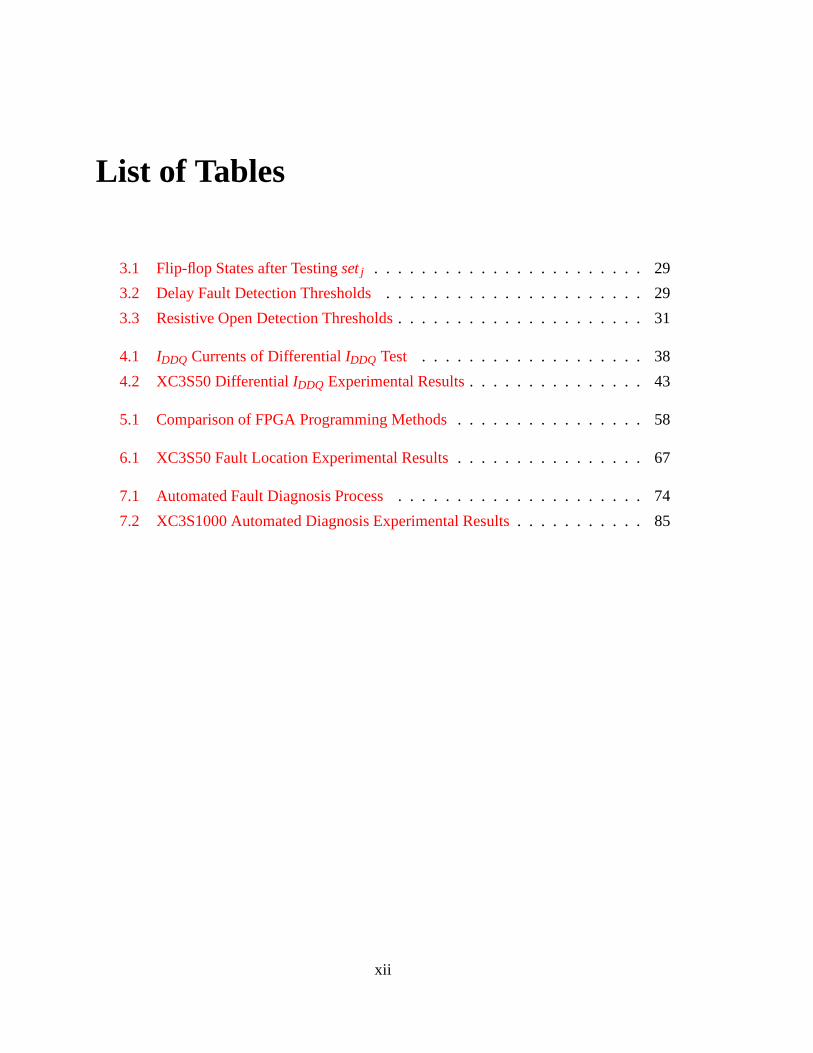
List of Tables
3.1 Flip-flop States after Testingsetj . . . . . . . . . . . . . . . . . . . . . . . 29
3.2 Delay Fault Detection Thresholds. . . . . . . . . . . . . . . . . . . . . . 29
3.3 Resistive Open Detection Thresholds. . . . . . . . . . . . . . . . . . . . . 31
4.1 IDDQ Currents of DifferentialIDDQ Test . . . . . . . . . . . . . . . . . . . 38
4.2 XC3S50 DifferentialIDDQ Experimental Results. . . . . . . . . . . . . . . 43
5.1 Comparison of FPGA Programming Methods. . . . . . . . . . . . . . . . 58
6.1 XC3S50 Fault Location Experimental Results. . . . . . . . . . . . . . . . 67
7.1 Automated Fault Diagnosis Process. . . . . . . . . . . . . . . . . . . . . 74
7.2 XC3S1000 Automated Diagnosis Experimental Results. . . . . . . . . . . 85
xii
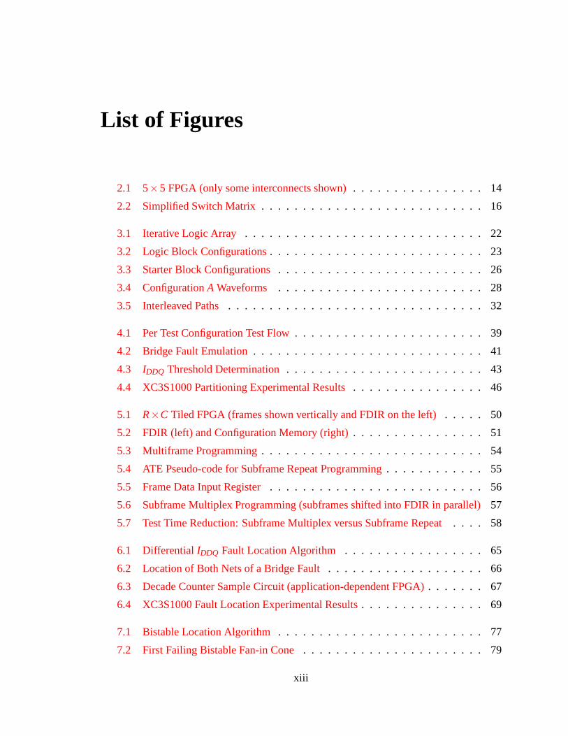
List of Figures
2.1 5×5 FPGA (only some interconnects shown). . . . . . . . . . . . . . . . 14
2.2 Simplified Switch Matrix. . . . . . . . . . . . . . . . . . . . . . . . . . . 16
3.1 Iterative Logic Array . . . . . . . . . . . . . . . . . . . . . . . . . . . . . 22
3.2 Logic Block Configurations. . . . . . . . . . . . . . . . . . . . . . . . . . 23
3.3 Starter Block Configurations. . . . . . . . . . . . . . . . . . . . . . . . . 26
3.4 ConfigurationA Waveforms . . . . . . . . . . . . . . . . . . . . . . . . . 28
3.5 Interleaved Paths. . . . . . . . . . . . . . . . . . . . . . . . . . . . . . . 32
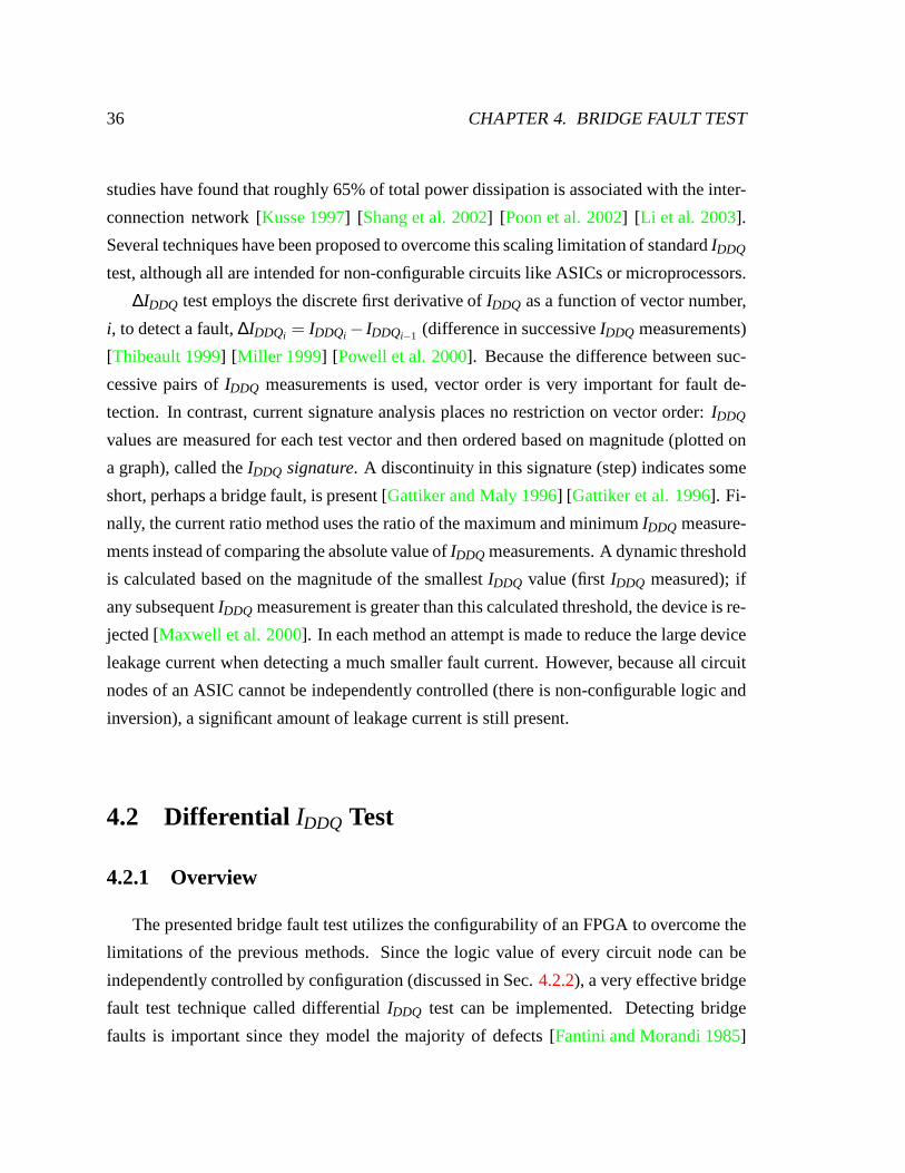
4.1 Per Test Configuration Test Flow. . . . . . . . . . . . . . . . . . . . . . . 39
4.2 Bridge Fault Emulation. . . . . . . . . . . . . . . . . . . . . . . . . . . . 41
4.3 IDDQ Threshold Determination. . . . . . . . . . . . . . . . . . . . . . . . 43
4.4 XC3S1000 Partitioning Experimental Results. . . . . . . . . . . . . . . . 46
5.1 R×C Tiled FPGA (frames shown vertically and FDIR on the left). . . . . 50
5.2 FDIR (left) and Configuration Memory (right). . . . . . . . . . . . . . . . 51
5.3 Multiframe Programming. . . . . . . . . . . . . . . . . . . . . . . . . . . 54
5.4 ATE Pseudo-code for Subframe Repeat Programming. . . . . . . . . . . . 55
5.5 Frame Data Input Register. . . . . . . . . . . . . . . . . . . . . . . . . . 56
5.6 Subframe Multiplex Programming (subframes shifted into FDIR in parallel) 57
5.7 Test Time Reduction: Subframe Multiplex versus Subframe Repeat . . . . 58
6.1 DifferentialIDDQ Fault Location Algorithm . . . . . . . . . . . . . . . . . 65
6.2 Location of Both Nets of a Bridge Fault. . . . . . . . . . . . . . . . . . . 66
6.3 Decade Counter Sample Circuit (application-dependentFPGA) . . . . . . . 67
6.4 XC3S1000 Fault Location Experimental Results. . . . . . . . . . . . . . . 69
7.1 Bistable Location Algorithm. . . . . . . . . . . . . . . . . . . . . . . . . 77
7.2 First Failing Bistable Fan-in Cone. . . . . . . . . . . . . . . . . . . . . . 79
xiii

7.3 Routing Net (path with fan-out). . . . . . . . . . . . . . . . . . . . . . . 82
7.4 Potentially Faulty PIPs (bold). . . . . . . . . . . . . . . . . . . . . . . . . 85
xiv

Part I
Fundamentals
1
Chapter 1
Introduction
1.1 Background
1.1.1 Field-programmable Gate Array
A Field-programmable Gate Array(FPGA) is a configurable integrated circuit that can
implement an arbitrary logic design. An FPGA can be repeatedly programmed to permit
fast and inexpensive prototyping, product development, and design error correction. Proto-
typing, or emulation, is the modeling and simulation of all aspects of a logic design whose
final implementation is not FPGA-based, while product development is the design, analy-
sis, and test of a logic design whose final implementation is FPGA-based. Because fabrica-
tion is required forApplication-specific Integrated Circuits(ASICs), the development time
(time to production) of ASIC-based designs is greater than ayear and theNon-recurring
Engineering(NRE) costs are tens of millions of dollars [ITRS 2003]. However, because
FPGA-based designs do not require fabrication (an FPGA is simply programmed with a
logic design), a much shorter development time and much lower NRE results, which has led
to the current popularity of FPGAs for product development and prototyping. FPGA-based
products have the additional benefit that design errors discovered after product release can
be corrected by simply reprogramming the FPGA with the corrected design, called field-
upgrading. Note that ASICs are better suited for high-volume designs since the cost of
ASIC NRE, amortized per chip, is typically less than the expensive cost per FPGA.
An FPGA is organized as a two-dimensional array of logic blocks and input/output
2
1.1. BACKGROUND 3
blocks that are joined by an interconnection network. The size, functionality, and perfor-
mance of an FPGA varies both within and between devicefamilies(a series of differently
sized FPGAs that share a common architecture). A particulardevice family and size is cho-
sen for implementation based on the specifications of a logicdesign. With up to 8 million
system gates and 3 Mb of dual-portRead-only Memory(RAM), a maximum internal clock
frequency of 420 MHz, and input/output data rates reaching 840 Mb/s [Xilinx, Inc. 2001],
implementation of very large and complicated designs is possible. Although internal clock
frequencies are slower than those for ASICs, the arrayed structure, configurable logic ele-
ments, and abundant routing resources of an FPGA permit highly parallel computation that
yields increased throughput. Applications in networking,Digital Signal Processing(DSP),
graphics, and cryptography, among others, can be efficiently implemented.
1.1.2 FPGA Manufacturing
For correct functionality, the resources used to implementa logic design must be defect-
free. A defectis a physical imperfection, introduced during manufacturing, that causes
an FPGA to function incorrectly. A device is tested to detectdefects, thereby ensuring
an Acceptable Quality Level(AQL), a measure of the number of defective devices that
escape manufacturing test (lower AQL means fewer defectiveoutgoing devices). Although
desired, there is no guarantee that a device is defect-free because it passes manufacturing
test: tests are imperfect and unable to detect all defects.
FPGA test is the responsibility of the manufacturer. Anapplication-independentFPGA
is one whose configuration may change throughout its lifetime. Because the manufacturer
cannot know which logic and routing resources of an application-independent FPGA a cus-
tomer will use and because literally billions of configurations are possible (all of which can-
not be tested), special techniques and tools are required for test. In contrast, anapplication-
dependentFPGA is one whose configuration remains unchanged throughout its lifetime,
useful for low- to medium-volume or cost sensitive logic designs. Because the logic de-
sign for an application-dependent FPGA is not allowed to change [Xilinx, Inc. 2003c] (the
manufacturer knows which logic and routing resources will be used by a customer), testing
4 CHAPTER 1. INTRODUCTION
an application-dependent FPGA is much simpler than testingan application-independent
FPGA: used resources must be defect-free but unused resources may be defective.
Although most devices that fail manufacturing test are discarded, some are diagnosed
to determine the cause of failure. The information obtainedfrom diagnosis is used to make
manufacturing improvements to increase yield.Yield—a measure of the number of defect-
free manufactured devices—is the hallmark of a good manufacturing process: high yield
means few defective devices. However, FPGA diagnosis is difficult and time-consuming,
primarily due to the complexity of the configurable interconnection network. Like FPGA
test, special techniques and tools are required for diagnosis.
1.1.3 Defects and Faults
As stated, a defect is a physical imperfection introduced during manufacturing that
causes device failure. However, the physical nature of a defect, which can have a very
complicated behavior, does not permit direct mathematicaltreatment of test and diagnosis.
Thus, the logical effect of a defect is modeled by afault, and detection or identification
of defects is accomplished by detection or identification offaults (with the exception of
defect-based test, which is the detection of defects by measuring some device parameter,
for example a particular current magnitude or voltage level). Note that aflaw is also a
physical imperfection; however, it causes device failure after some time period (flaw de-
grades into defect). Flaws and the screen required to eliminate flaws are not discussed in
this dissertation.
There are several common fault models: stuck-at, bridge, and delay, among others.
A stuck-at faultis a fixed logic value on a circuit node, either stuck-at 0 or stuck-at 1,
regardless of the value driven on that node. Abridge fault is the logical behavior of a
bridge, for example wired-AND or wired-OR, caused by a shortbetween signal lines that
should not be connected. Finally, adelay fault is an additional delay on some path or
through some gate in a circuit that causes timing failures.
Throughout this dissertation an attempt is made not to mix the usage of the terms defect
and fault. For example, in Chap.3 detection of delay faults, not delay defects, is discussed
since the cause of delay is irrelevant while in Chap.4 the resistance of a bridge—a physical
1.2. CONTRIBUTIONS 5
quantity—is writtenRde f ect. However, in Chap.4 the current caused by a bridge is referred
to as a fault current, not defect current, to be consistent with the terminology used in the
literature.
1.2 Contributions
To cope with defects, an FPGA manufacturer must execute two essential tasks: (1)
thorough test to ensure high device quality, and (2) efficient diagnosis to achieve high man-
ufacturing yield. Because of the distinct architectural and functional differences between
ASICs and FPGAs, many test and diagnosis techniques for ASICs are not applicable to
FPGAs. Additionally, because the interconnection networkconstitutes up to 80% of the
die area and up to 8 metal layers of an FPGA, it is the primary focus in both tasks. This
dissertation summarizes my contributions to the fields of FPGA test and diagnosis.
1.2.1 Test
Delay Fault Test
The objective of test is to detect defects. Most tests are based on the stuck-at fault
model, which is used primarily because of its simplicity [McCluskey 1993]. There
are several effective techniques to detect stuck-at faultsin FPGAs, some consider-
ing only faults in the logic blocks [Stroud et al. 1996] [Huang and Lombardi 1996]
[Renovell and Zorian 2000] and some considering faults in the interconnection
network [Renovell et al. 1997a] [Wang and Huang 1998] [Renovell et al. 1998]
[Doumar and Ito 1999] [Sun et al. 2001] [Tahoori and Mitra 2003]. However, it is well
known that stuck-at faults do not accurately model defects [McCluskey and Tseng 2000]
[McCluskey et al. 2004], for example a defect causing a delay fault.
Detecting delay faults, which cause timing failures in an otherwise functioning FPGA,
is difficult due to the slow test speeds of contemporaryAutomated Test Equipment(ATE).
At slow test speeds, path slack—the difference between the actual time a signal on a
path stabilizes and the time at which the signal must be stable—is so large that even a
delay fault may not cause a failure (a negative path slack). Amethod is developed in
6 CHAPTER 1. INTRODUCTION
[Abramovici and Stroud 2002] that detects delay faults in both the interconnection network
and the logic blocks; however, the test configurations implement long paths of interconnects
and logic elements, which (1) fail if either one large delay fault (spot defect) or many small
delay faults (process variation) are present along the path(which may or may not be de-
sired), and (2) increase the likelihood offault masking, or the inability to detect a fault due
to the presence of another. A different method is developed in [Tahoori 2002b] that detects
resistive opens (which can cause delay faults) in the interconnection network of an FPGA;
however, it is only applicable to older FPGA architectures,for example Xilinx XC3000
and XC4000).
In this dissertation a delay fault detection technique is presented that has
several advantages over the previous techniques. Comparedto the method in
[Abramovici and Stroud 2002], the test configurations implement the shortest possible
paths under test to decrease the likelihood of fault masking; compared to the method
in [Tahoori 2002b], the presented technique is independent of FPGA architecture. By
creating a controlled signal race on paths of equal fault-free propagation delay and
observing if one signal transitions much later than another, very small (nanosecond) delay
faults can be detected with slow ATE [Chmelar 2003]. Test configurations are developed to
detect delay faults of various sizes (independent of FPGA architecture), utilizingIterative
Logic Arrays(ILAs) to permit the test configurations to scale with FPGA size.
Bridge Fault Test
A bridge is a short between signal lines that should not be connected, which usu-
ally causes a fault current when activated (bridged circuitnodes are driven to opposite
logic values). This fault current can be observed by measuring the steady-state current
drawn by a device,IDDQ. IDDQ test is important for FPGAs because of the large number
of transmission-gate multiplexers in the interconnectionnetwork, in which certain bridge
faults can only be detected viaIDDQ test [Makar and McCluskey 1996]. However, the ef-
fectiveness ofIDDQ test is limited due to the shrinking geometries of deep sub-micron
processes. Scaling of threshold voltages has caused transistor leakage currents to increase,
thereby exponentially increasingIDDQ but not correspondingly increasing fault currents.
There are several test methods that address this scaling limitation of standardIDDQ
1.2. CONTRIBUTIONS 7
test, for example∆IDDQ test [Thibeault 1999] [Miller 1999] [Powell et al. 2000], cur-
rent signature analysis [Gattiker and Maly 1996] [Gattiker et al. 1996], and current ratios
[Maxwell et al. 2000]; however, all are intended for non-configurable circuits like ASICs
or microprocessors.
In this dissertation a technique called differentialIDDQ test is presented that overcomes
this IDDQ scaling problem for FPGAs, employing the configurability ofan FPGA to detect
bridge faults [Chmelar and Toutounchi 2004]. By using the difference in a pair ofIDDQ
measurements (rather than a single measurement), a significant portion of the device leak-
age current can be cancelled to more easily observe a small fault current (the logic value of
each circuit node can be controlled independently with special test configurations, which is
not possible in non-configurable circuits like ASICs or microprocessors). Bridge faults in
an FPGA are activated simply by programming the device with several test configurations
that take advantage of the regular structure of the interconnection network (application of
test vectors is not required). Because measuringIDDQ takes roughly 20 ms—a long time
when testing a device—in practice only a few measurements are taken (around 10 or 20),
limiting the number of possible bridge faults that can be activated and therefore detected.
It is shown that only 5 configurations, and thus 5IDDQ measurements (one measurement
per configuration), can detect all interconnect bridge faults in contemporary FPGAs. Addi-
tionally, the fault current detectability (size of the fault current compared to the magnitude
of the IDDQ) can be increased bypartitioning, or dividing, the nets of a test configuration
into subsets, each of which corresponds to a new, smaller test configuration.
Test Time Reduction
The configuration time—the time required to program an FPGA with a test
configuration—consumes the majority of total test time, andtherefore dominates test cost.
To significantly decrease the test time of an FPGA, a reduction must be made in either (1)
the number of test configurations, or (2) the configuration time.
Several test configuration generation techniques have beenproposed to alleviate this
test time problem by reducing the number of test configurations. Although most tech-
niques consider only detection of faults in the logic resources [Renovell et al. 1997b]
[Renovell et al. 1999a] [Renovell et al. 1999b], some do consider detection of faults in the
8 CHAPTER 1. INTRODUCTION
interconnection network [Sun et al. 2002a] [Sun et al. 2002b] [Tahoori and Mitra 2003].
Those that consider faults in the interconnection network derive a reduced number of test
configurations using interconnect modeling and graph traversal algorithms. Rather than re-
duce the number of test configurations, test time can be made shorter by reducing the con-
figuration time (time required to program an FPGA under test with each test configuration).
A modified configuration memory architecture is proposed in [Doumar and Ito 1999] that
allows internal shifting of test configuration data within an FPGA, thereby reducing the
number of test configurations that must be externally programmed into the device under
test. However, it assumes the configuration memory is structured as a single scan chain.
Furthermore, the specially designed test configuration that is internally shifted within an
FPGA detects only faults in the logic resources.
In this dissertation a technique is presented that reduces the configuration time
to decrease total test time [Chmelar 2004b] [Chmelar 2004c]. Unlike the method in
[Doumar and Ito 1999], the presented technique (1) can detect faults in either the logic or
routing resources, and (2) is applicable to contemporary FPGA architectures, whose config-
uration memory is organized as an SRAM array. Because the presented technique reduces
only the configuration time, it can be used in conjunction with those methods that reduce
the number of test configurations. A small amount ofDesign for Test(DFT) hardware—
several 2-bit multiplexers (R− 3 in total for anR×C FPGA)—is added to the existing
FPGA hardware. These multiplexers, which take advantage ofthe regular structure of both
an FPGA and each test configuration, permit parallel programming of test configuration
data, achieving a configuration time reduction of approximately 40%. By reducing the
configuration time, the number of test configurations can be increased to achieve a more
thorough FPGA test without increasing test cost.
1.2.2 Diagnosis
Bridge Fault Location
The objective of diagnosis is to locate or identify defects.Fault location is an important
part of fault diagnosis since it is usually necessary to locate a fault to identify the underlying
defect. Because the majority of an FPGA is its interconnection network and due to the high
1.2. CONTRIBUTIONS 9
density of the physical layout in deep sub-micron process technologies, locating faults in
the interconnection network is an important concern in FPGAs.
There are many Boolean techniques that can locate a stuck-atfault in an FPGA
[Wang and Huang 1998] [Yu et al. 1998] [Wang and Tsai 1999] [Abramovici et al. 1999]
[Das and Touba 1999] [Yu et al. 1999] [Abramovici and Stroud 2000]
[Harris and Tessier 2000a] [Stroud et al. 2001] [Abramovici and Stroud 2001]
[Lu and Chen 2002] [Stroud et al. 2002] [Harris and Tessier 2002]. However, be-
cause bridge faults model the majority of defects [Fantini and Morandi 1985]
[Ferguson and Larrabee 1991] and since certain bridge faults can only be detected
(and therefore located) viaIDDQ test [Makar and McCluskey 1996], it is important to be
able to locate a bridge fault usingIDDQ measurements.
This dissertation presents an interconnect bridge fault location technique that uses only
device configuration andIDDQ measurements [Chmelar and Toutounchi 2004]. By itera-
tively partitioning the nets of the test configuration for which the FPGA failed differential
IDDQ test and independently testing the FPGA with each partition, fault-free nets can be
progressively eliminated until only a faulty net—one of thebridged nets—remains (the
other bridged net is found by applying the location process asecond time using a comple-
mentary test configuration). Very few configurations andIDDQ measurements are required,
logarithmic in the number of nets in the test configuration. Furthermore, because of the
simplicity in partitioning—accomplished by device configuration alone—the process can
be easily automated.
Automated Fault Diagnosis
When the type of defect present is not known (unknown cause offailure), both iden-
tification and location must be conducted. A common method isstuck-at fault diagnosis
(the stuck-at fault model is again chosen primarily for its simplicity), which (1) uses stuck-
at faults to model the behavior of a defect, and (2) identifiesthe smallest possible set of
fault candidates, or faults that could explain the failure (explain the output response of the
defective device).
In practice FPGAs are diagnosed using a manual andad hoc process which
10 CHAPTER 1. INTRODUCTION
takes days to weeks to diagnose a single device. There are several formal diagno-
sis techniques that attempt to reduce this diagnosis time, all based on generating
in advance a set of test configurations and test vectors whoseoutput responses
in the presence of a fault can be used to identify the fault. Some techniques
diagnose only faults in the logic resources of an FPGA [Wang and Tsai 1999]
[Abramovici and Stroud 2000] [Abramovici and Stroud 2001] [Lu and Chen 2002] while
others also diagnose faults in the interconnection network[Wang and Huang 1998]
[Yu et al. 1999] [Abramovici et al. 1999] [Harris and Tessier 2000a] [Stroud et al. 2001]
[Stroud et al. 2002] [Harris and Tessier 2002]. However, for all techniques a unique set of
test configurations and test vectors must be generated for each differently sized FPGA of a
particular architecture. Furthermore, the set of test configurations and test vectors must be
regenerated (if possible) for different FPGA architectures.
This dissertation presents an automated FPGA diagnosis technique that has several ad-
vantages over the previous techniques. Compared to thead hocdiagnosis seen in prac-
tice that requires several days or weeks to diagnose a singledevice, the diagnosis time of
the presented method is reduced to only several hours; compared to the formal diagno-
sis techniques, the presented technique is (1) capable of diagnosing any fault detectable
by the manufacturing test configurations, and (2) applicable to any FPGA architecture in
production. By taking advantage of the configurability of anFPGA to make use of the al-
ready existing manufacturing test configurations, a set of fault candidates (stuck-at faults)
is determined by testing the FPGA with all (or at least many) of the manufacturing test
configurations (testing is not stopped after the first failure) [Chmelar 2004a]. Next, the
set of fault candidates is reduced by locating the first bistable (or bistables) to capture a
faulty value (result of fault activation) in several of the test configurations for which the
FPGA failed, accomplished by comparing the state of the FPGAbeing diagnosed to that
of a known good FPGA that is tested in exactly the same manner.Finally, the set of fault
candidates is further reduced by systematically eliminating faults that are (1) not common
to all test configurations for which the FPGA failed, and (2) shown not to exist by the test
configurations for which the FPGA passed.
1.3. OUTLINE 11
1.3 Outline
This dissertation presents new effective techniques for the test and diagnosis of FP-
GAs. Test is discussed in PartII (Chaps3 through5) and diagnosis is discussed in PartIII
(Chaps6 and7).
Chapter2 describes a generic FPGA structure. Logic and routing resources are dis-
cussed, as well as the basic hardware used to program the device.
Chapter3 presents a scalable FPGA interconnect delay fault test. Minimum detectable
delay fault sizes are calculated for 6 Xilinx FPGA families.
Chapter4 presents an interconnect bridge fault test using differential IDDQ. The im-
provement over standardIDDQ test is determined for Xilinx Spartan-3 FPGAs.
Chapter5 presents a simple DFT technique that significantly reduces the configuration
time for an FPGA under test. Time savings are calculated for Xilinx Virtex FPGAs.
Chapter6 presents a bridge fault location technique using differential IDDQ. Emulated
bridge faults are located on several Xilinx Spartan-3 FPGAs.
Chapter7 presents an automated stuck-at fault diagnosis technique.Diagnosis of both
logic and routing faults is conducted for several faulty Xilinx Spartan-3 FPGAs.
Chapter8 concludes this dissertation.

12 CHAPTER 1. INTRODUCTION
This page intentionally left blank.
Chapter 2
FPGA Structure
2.1 Overview
An FPGA is a two-dimensional array of blocks that are joined by an interconnection
network. There are several types of blocks: logic blocks, input/output blocks, multiplier
blocks, and RAM blocks [Xilinx, Inc. 2002a]. Logic Blocks(LBs) contain the configurable
hardware for logic design implementation.Input/Output Blocks(IOBs) are used for pri-
mary inputs and outputs.Multiplier blocks(MBs) contain hardware to implement special-
ized arithmetic. Finally,RAM blocks(BRAMs) contain user-addressable memory arrays.
Since most blocks in an FPGA are logic blocks and very few are multiplier or RAM blocks,
an FPGA is basically a regular array of logic blocks. The interconnection network consists
of interconnects, switch matrices or multiplexers, and buffers. An interconnectis a wire
segment. ASwitch Matrix (SM), or programmable multiplexer, is used to join blocks.
Buffersare used in the same manner as they are for any interconnection network.
The arrayed layout of an FPGA is achieved using tiles [Tavana et al. 1996]
[Tavana et al. 1999]. There are only a few types of tiles: a logic block and its associated
switch matrix make anLB tile while an input/output block and its associated switch matrix
make anIOB tile (for simplicity multiplier blocks and RAM blocks are not discussed).
Local routing (interconnects) is included in each tile.
An FPGA is organized as an array ofR rows andC columns. One row, containingC
tiles, spans the entire width of the device. Similarly, one column, containingR tiles, spans
the entire height of the device. The leftmost and rightmost columns in an FPGA areIOB
columnswhile the middle columns areLB columns. Each IOB column containsR IOB tiles;
13
14 CHAPTER 2. FPGA STRUCTURE
each LB column containsR−2 LB tiles and 2 IOB tiles. Thesizeof an FPGA, given in
terms of the number of rows and columns, respectively, describes the total number of tiles.
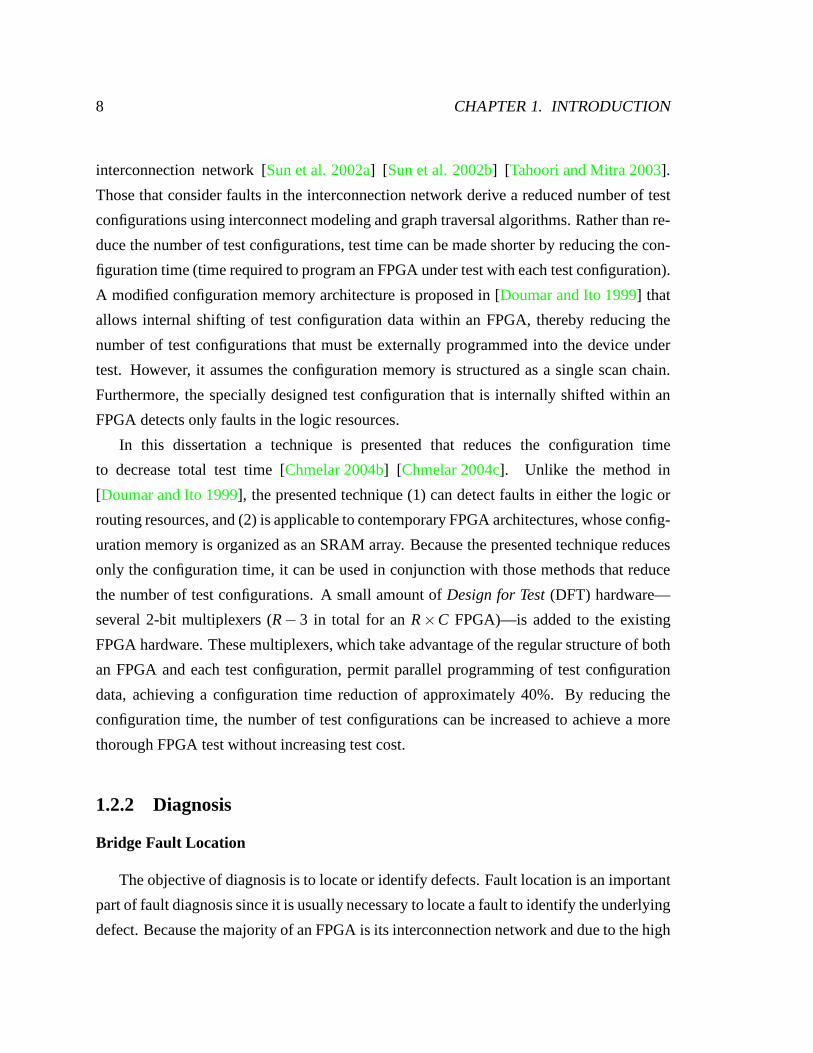
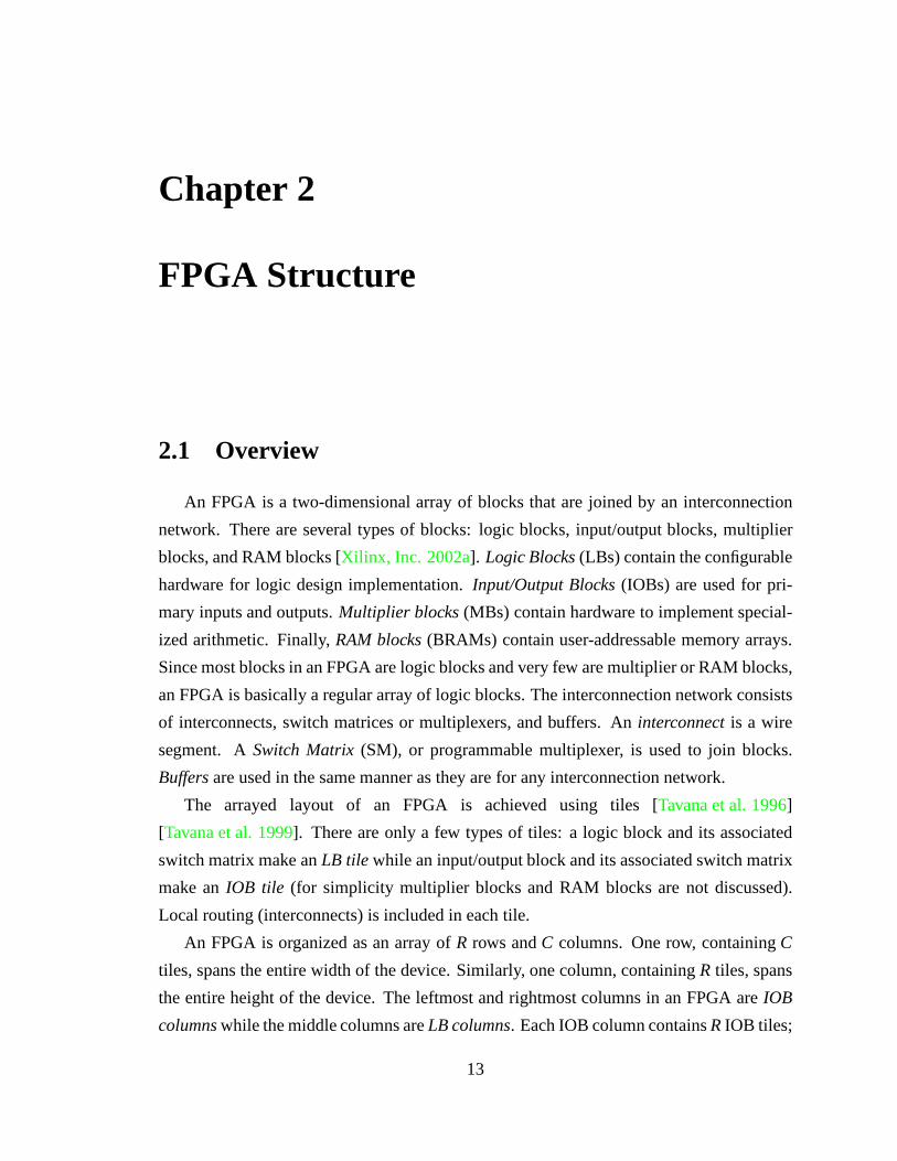
Figure2.1shows a simplified 5×5 FPGA with logic blocks in the center and input/output
blocks on the periphery: the upper left half shows the tile representation while the lower
right half shows the switch matrices, blocks, and a subset ofthe interconnects.
Interconnect
Switch Matrix
Logic Block
Interconnect
Switch Matrix
Logic Block
Interconnect
Switch Matrix
Logic Block
Interconnect
Switch Matrix
Logic Block
IOB Tile IOB TileIOB Tile
IOB Tile
IOB Tile
Interconnect
Switch Matrix
Logic Block
colu
mn 5
colu
mn 4
colu
mn 3
colu
mn 2
colu
mn 1
LB Tile
row1
row 2
row 3
row 4
row 5
Interconnect
Switch Matrix
Logic Block
Input/Output Block
Switch MatrixSwitch Matrix
Input/Output Block
Switch Matrix
Input/Output Block
Switch Matrix
Input/Output Block
Switch Matrix
Input/Output Block
Interconnect
Input/Output Block
Switch Matrix
Interconnect
Input/Output Block
Switch Matrix
Interconnect
Input/Output Block
Switch Matrix
Interconnect
Input/Output Block
Switch Matrix
Figure 2.1: 5×5 FPGA (only some interconnects shown)
2.2. LOGIC RESOURCES 15
2.2 Logic Resources
A logic block contains the combinational and sequential elements needed to implement
arbitrary logic functions. In the Xilinx Virtex architecture—the same basic architecture
of most contemporary FPGAs—a logic block is subdivided intotwo smaller units, called
slices. Eachslicecontains twoLook-up Table(LUTs) and two bistables, as well as some
carry logic and several small multiplexers. A single look-up table can implement any 4-
input combinational logic function; multiple look-up tables can be combined to implement
larger functions. A look-up table is a small array of memory,16×1 bits, that stores the
truth table of a 4-input Boolean function (24 = 16 values). A bistable, used to implement
sequential functions, can be configured to operate as eithera D latch or a D flip-flop.
2.3 Routing Resources
A net is the concatenation of several interconnects, or wire segments, that form a path
between blocks. In contemporary FPGAs, interconnects are hierarchically organized by
length and direction. In the Virtex architecture, there arethree lengths, single, hex, and
long, each routed either horizontally or vertically for a total of six types. Single lines
interconnect adjacent switch matrices in all four directions. Hex lines interconnect every
third and sixth switch matrix in all four directions. Finally, long lines span the entire height
or width of a device. The majority of an FPGA is its interconnection network, constituting
up to 80% of the die area and up to 8 metal layers.
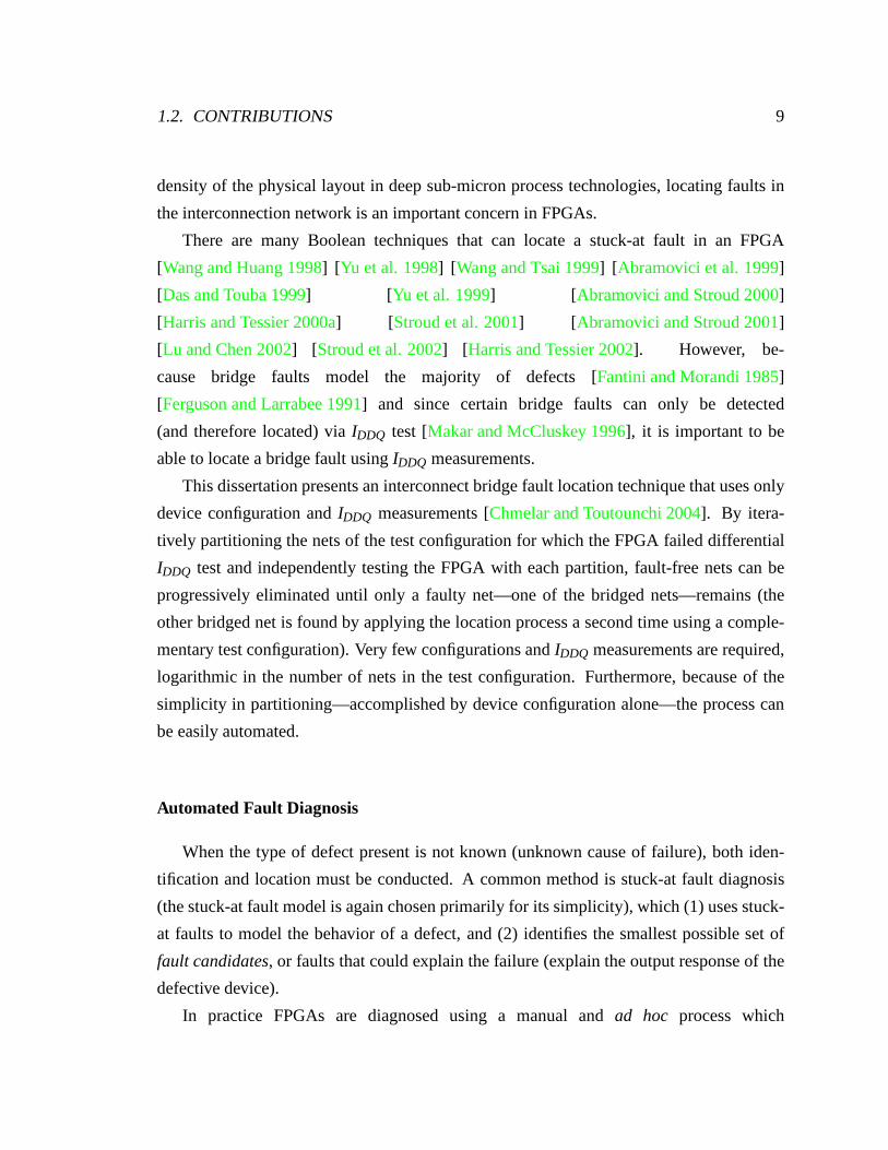
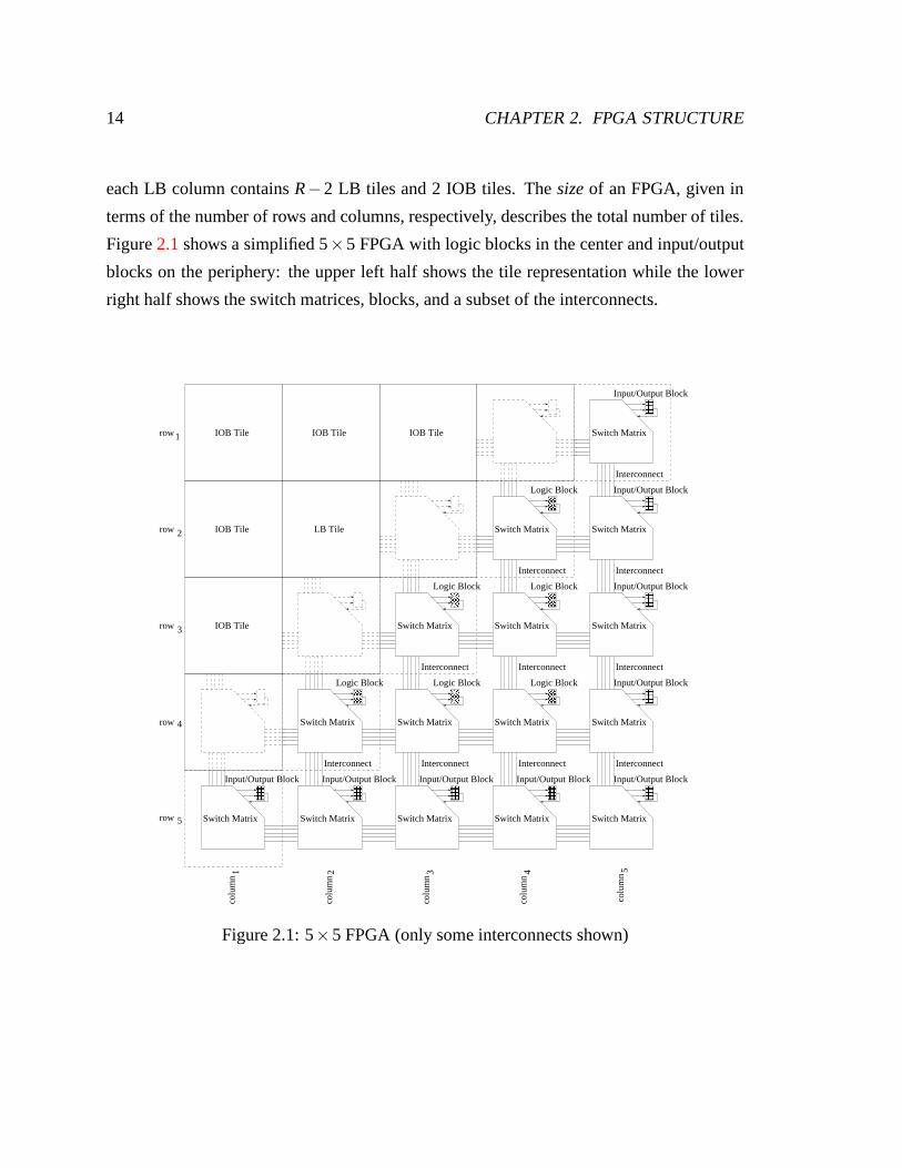
Routing of nets is accomplished by switch matrices, which either join interconnects
to (1) block inputs or outputs, or (2) other interconnects. The configurability of a switch
matrix is achieved byProgrammable Interconnect Points(PIPs). A PIP is a pass transistor
controlled by an associated memory cell that determines whether the transistor ison (con-
ducting) oroff (non-conducting). Figures2.2aand2.2bshow the directed graph represen-
tation of a simplified switch matrix, Fig.2.2cshows the PIP implementation, and Fig.2.2d
shows the path of a net that joins two logic blocks through several switch matrices.
16 CHAPTER 2. FPGA STRUCTURE
i1
o1i2
E W
S
N Logic Block
(a) Fully Connected
! ! !! ! !! ! !! ! !! ! !i1
o1i2
E W
S
N Logic Block
(b) Not Fully Connected
M
M
" " "" " "" " "" " "" " "# # ## # ## # ## # ## # #i1
o1i2
E W
S
N Logic Block
(c) PIP Implementation
$ $ $$ $ $$ $ $$ $ $$ $ $$ $ $% % %% % %% % %% % %% % %% % %
& & && & && & && & && & && & &' '' '' '' '' '' '
( (( (( (( (( (( () )) )) )) )) )) )
i1
o1i2
E W
S
N Logic Blocki1
o1i2
E W
S
N Logic Blocki1
o1i2
E W
S
N Logic Block
Net
(d) Path of Net through Switch Matrices
Figure 2.2: Simplified Switch Matrix
2.4 Configuration
An FPGA must beconfigured, or programmed with a logic design, before it can func-
tion. Each FPGA contains special configuration hardware that is used to program the de-
vice and configuration memory that stores the configuration data. Theconfiguration data
determines which logic and routing resources are used and inwhat manner.
Theconfiguration memoryis an array of SRAM cells, distributed throughout an FPGA,
that is programmed via vertical address lines and horizontal data lines. The smallest unit of
memory that can be independently programmed, called aframe, is a 1-bit wide column of
memory that spans the entire height of the device. Each column of tiles, either an LB or IOB
column, contains 48 frames (48 frames wide) in the Virtex architecture [Xilinx, Inc. 2002b]
[Xilinx, Inc. 2003b].
Theconfiguration hardwareconsists of the configuration memory addressing logic that
is used to address a given frame of memory and theFrame Data Input Register(FDIR)
that is used to serially shift in configuration data before programming the configuration
memory. The FDIR is a single-input scan chain spanning allR rows of an FPGA: it stores
2.4. CONFIGURATION 17
exactly one frame of configuration data. Thus, programming an FPGA with a complete
configuration consists of many iterations of: (1) shift the configuration data of a single
frame into the FDIR, and (2) write the contents of the FDIR to aparticular address (frame
location) in the configuration memory. The smallest Virtex FPGA takes approximately
4 ms to program; the largest takes approximately 8 ms (an example calculation is provided
in Chap.5).
Contemporary FPGAs—Xilinx FPGAs since the XC4000 architecture—have an addi-
tionalDesign for Test(DFT) feature calledreadback, which enables both the configuration
data and the state of all bistables to be serially scanned outof the device (conceptually the
inverse of configuration) [Holfich 1994]. Capturing the state of an FPGA at any time via
readback is useful for design validation and fault diagnosis.

18 CHAPTER 2. FPGA STRUCTURE
This page intentionally left blank.

Part II
Test
19
Chapter 3
Delay Fault Test
3.1 Motivation and Previous Work
There are effective test methods that detect stuck-at and stuck open faults in application-
independent FPGAs, some considering only faults in the logic blocks [Stroud et al. 1996]
[Huang and Lombardi 1996] [Renovell and Zorian 2000] and some considering faults
in the interconnection network [Renovell et al. 1997a] [Wang and Huang 1998]
[Renovell et al. 1998] [Doumar and Ito 1999] [Sun et al. 2001] [Tahoori and Mitra 2003].
However, only recently has testing for delay faults been addressed [Krasniewski 2001]
[Harris et al. 2001] [Abramovici and Stroud 2002] [Tahoori 2002b].
Detecting delay faults is difficult due to the slow test speeds of contemporaryAutomated
Test Equipment(ATE); however, it is important for two reasons: a delay fault (1) can
cause timing failures in an otherwise functioning device [Li et al. 2001] [Tahoori 2002c],
and (2) may result in an early-life failure (device prematurely stops functioning) if it is
caused by aresistive open—a partially conducting circuit path. A study of microprocessors
(manufactured in high volume) found that 58% of customer-returned devices had some type
of open defect, a significant portion of which were resistiveopens [Needham et al. 1998].
The method in [Tahoori 2002b] detects resistive opens in the interconnection net-
work by activating one or more unused PIPs along a path under test to increase the
load (fan-out) on the path. The additional load increases the RC delay of the path un-
der test, resulting in a negative path slack if a resistive open is present. Although ef-
fective, the method is only applicable to FPGAs whose switchmatrices and PIPs are
not implemented as multiplexers (XC3000 and XC4000 architectures are not multiplexer
20
3.2. DELAY FAULT DETECTION 21
based, Virtex, Virtex-II and Spartan-3 architectures are multiplexer-based). The method in
[Abramovici and Stroud 2002] detects delay faults in both the interconnection network and
the logic blocks by observing the difference in propagationdelays between a pair of paths
under test. Long paths consisting of both logic elements andinterconnects are configured
to have approximately equal fault-free propagation delays. A signal transition is simulta-
neously driven at the input of each path, and the difference in the propagation delays is
measured at the outputs by means of an on-chip oscillator. However, test configurations
that contain long paths of interconnects and logic elementswill fail if either one large de-
lay fault (spot defect) or many small delay faults (process shift) are present along the path,
which may or may not be desired. Additionally, the probability of fault masking, or the
inability to detect a fault due to the presence of another, ishigher for longer paths.
3.2 Delay Fault Detection
3.2.1 Overview
The presented delay fault test is applicable to all contemporary FPGA architectures.
Severalpaths under test, consisting of a set of interconnects and PIPs between two logic
blocks, are configured to have equal fault-free propagationdelays. A race between the sig-
nals on the paths is started at the first logic block and the difference in transition times of
the signals at the second logic block is observed. If the difference is above a predetermined
threshold (one signal transitions much later than the others), a delay fault is detected. By
configuring the shortest possible paths under test that do not include logic elements (PIPs
and interconnects only), the probability of fault masking—the result of a delay fault on
multiple paths—is minimized. The tiled structure of contemporary FPGAs and the hier-
archical organization of the interconnects easily facilitates the configuration of short paths
with nearly equal fault-free propagation delays.
In the FPGA under test, many logic blocks are consecutively joined by paths under
test, forming one or moreIterative Logic Array(ILA) as shown in Fig.3.1. Each logic
block of an ILA, sayLBi must (1) observe the relative transition times of the racingsignals
on its input paths, and (2) create signal races on its output paths. Therefore, each logic
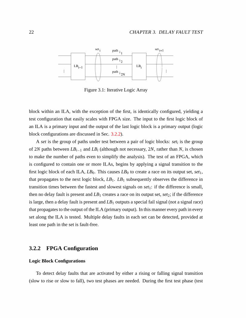
22 CHAPTER 3. DELAY FAULT TEST
LBi
iset
LBi−1
i+1setipath1
ipath2
path i 2N
Figure 3.1: Iterative Logic Array
block within an ILA, with the exception of the first, is identically configured, yielding a
test configuration that easily scales with FPGA size. The input to the first logic block of
an ILA is a primary input and the output of the last logic blockis a primary output (logic
block configurations are discussed in Sec.3.2.2).
A set is the group of paths under test between a pair of logic blocks: seti is the group
of 2N paths betweenLBi−1 andLBi (although not necessary, 2N, rather thanN, is chosen
to make the number of paths even to simplify the analysis). The test of an FPGA, which
is configured to contain one or more ILAs, begins by applying asignal transition to the
first logic block of each ILA,LB0. This causesLB0 to create a race on its output set,set1,
that propagates to the next logic block,LB1. LB1 subsequently observes the difference in
transition times between the fastest and slowest signals onset1: if the difference is small,
then no delay fault is present andLB1 creates a race on its output set,set2; if the difference
is large, then a delay fault is present andLB1 outputs a special fail signal (not a signal race)
that propagates to the output of the ILA (primary output). Inthis manner every path in every
set along the ILA is tested. Multiple delay faults in each setcan be detected, provided at
least one path in the set is fault-free.
3.2.2 FPGA Configuration
Logic Block Configurations
To detect delay faults that are activated by either a rising or falling signal transition
(slow to rise or slow to fall), two test phases are needed. During the first test phase (test
3.2. DELAY FAULT DETECTION 23
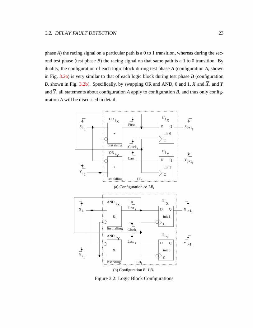
phaseA) the racing signal on a particular path is a 0 to 1 transition,whereas during the sec-
ond test phase (test phaseB) the racing signal on that same path is a 1 to 0 transition. By
duality, the configuration of each logic block during test phaseA (configurationA, shown
in Fig. 3.2a) is very similar to that of each logic block during test phaseB (configuration
B, shown in Fig.3.2b). Specifically, by swapping OR and AND, 0 and 1,X andX, andY
andY, all statements about configurationA apply to configurationB, and thus only config-
urationA will be discussed in detail.
Clocki
iFirst
ORXi
OR i Y
Y i 1LBi
iLast
X i 1X i+1
Y i+1
i Yff
i Xff
+ init 0
first rising
D Q
D Q
last falling
init 1+
C
C
1
1
(a) ConfigurationA: LBi
X i 1
LBi
Y i 1
Clocki
First i
AND i Y
ANDXi
Last i
X i+1
Y i+1
i Xff
i Yff
& init 1
first falling
D Q
last rising
&
1
1
C
init 0
D Q
C
(b) ConfigurationB: LBi
Figure 3.2: Logic Block Configurations
24 CHAPTER 3. DELAY FAULT TEST
Although the objective of the presented delay fault test is to detect delay faults,
bridge faults between paths can also be detected if the 2N paths of a particular set,
say seti, are divided into two groups (not necessarily of equal size), the X i = Xi1 . . .XiN
and Y i = Yi1 . . .YiN groups (discussed in Sec.3.2.5). Figures3.2aand3.2b show the
simplest case of one path in each group. During test phaseA, the creation of a
race onseti by LBi corresponds to the signal on eachXi j path simultaneously transi-
tioning from 0 to 1 and the signal on eachYi j path simultaneously transitioning from
1 to 0. One look-up table (ORiX ) of LBi is configured to implement the Boolean func-
tion Firsti = (Xi1 + . . .+XiN)+(Yi1 + . . .+YiN) = X i +Y i , where Firsti transitions from
0 to 1 after the signal on at least oneX i or Y i path transitions. Similarly, the
other look-up table (ORiY) of LBi is configured to implement the Boolean function
Lasti = (Xi1 + . . .+XiN)+(Yi1 + . . .+YiN) = X i +Y i , whereLasti transitions from 1 to 0
only after every signal on theX i andY i paths has transitioned.
TheFirsti signal is input to one of the D flip-flops ofLBi ( f fiX ) while theLasti signal is
input to the other D flip-flop (f fiY ). Additionally, theFirsti signal is fed back to the clock
input of both flip-flops, providing the mechanism to determine the difference in transition
times between the fastest and slowest signals on the paths ofseti. If there is more than
one X i or Y i path in seti, the fan-out from the single flip-flop output (f fiX or f fiY) is
accomplished via a switch matrix.
Racing Signal Transitions
If there is no delay fault on any path ofseti , then theFirsti andLasti signals transition
at approximately the same time. Thus, when theClocki signal transitions (the fed back and
therefore delayed version of theFirsti signal), the setup times for both thef fiX and f fiYflip-flops are satisfied and a new race is created onseti+1. In this manner, signal races are
created for each set in the ILA until the primary output is reached.
If, however, there is a delay fault on any path ofseti, then theLasti signal transitions
much later than theFirsti signal. Although the setup time for thef fiX flip-flop is satisfied
when theClocki signal transitions, the setup time for thef fiY flip-flop is not satisfied, and a
new race is not created onseti+1 (only the outputs off fiX , X i+1 paths, transition). Because
theY i+1 paths do not transition, the next logic block in the ILA,LBi+1, will detect a delay
3.2. DELAY FAULT DETECTION 25
fault (infinite delay), and it too will create a transition ononly itsX i+2 paths. When a logic
block transitions only itsX paths, it is said to output afail signal, which propagates to the
primary output of the ILA (each subsequent logic block outputs this fail signal).
Starter and Compactor Blocks
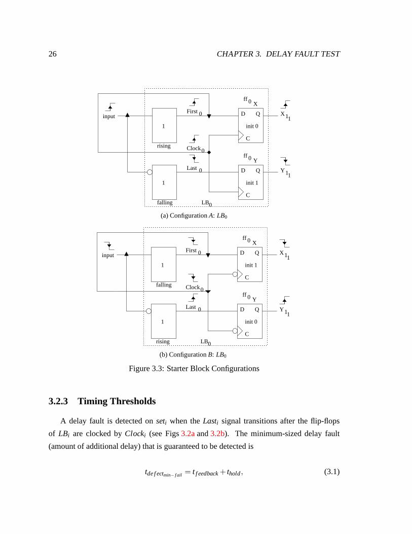
The function of the first logic block in each ILA,LB0, is only to create a signal race
on its output paths. Called the starter block, its configuration is similar to that of all other
logic blocks except it has only a single input (instead of multiple inputs). A single input
is used to (1) limit the number of primary inputs, and (2) eliminate the skew if multiple
signals were brought from off chip, which would undoubtedlyresult in an unfair race and
erroneous delay fault detection. Figures3.3aand3.3bshow the starter block configurations
for test phases A and B, respectively (each look-up table is configured as a buffer).
An additional logic block, called the compactor block (not shown), can be used to re-
duce the number of primary outputs, compacting the two outputs of the last logic block
in an M-length ILA, XM−11 and YM−11, into a single output. For test phaseA, one
look-up table of the compactor block is configured to implement the Boolean function
result= XM−11 ·YM−11, whereresult transitions only ifXM−11 andYM−11 transition (all
paths of the ILA passed). Similarly, for test phaseB, one look-up table of the compactor
block is configured to implement the Boolean functionresult= XM−11 ·YM−11, where
resultagain transitions only ifXM−11 andYM−11 transition.
ILA Scalability
The configuration of every logic block in an ILA (except the starter and compactor
blocks) is identical, enabling the size of an ILA to increasesimply by adding additional
logic blocks. Thus, the creation of ILAs, requiring only instantiation of identical logic
blocks throughout the FPGA, is a scalable procedure that is independent of FPGA size. Ad-
ditionally, configuring paths of equal fault-free propagation delay is easily accomplished by
automated place-and-route software tools. Finally, sinceonly the configuration of the logic
blocks changes between test phases (routing of paths is not altered), partial reconfiguration
can be used to significantly reduce total test time [Xilinx, Inc. 2003a].
26 CHAPTER 3. DELAY FAULT TEST
input
0Last
First 0
Clock0
LB0
X 1
0 Yff
0 Xff
Y 1
init 0
rising
falling
init 1
D Q
D Q
1
C
C
1
1
1
(a) ConfigurationA: LB0
input
Last 0
0Clock
First 0
LB0
X 1
Y 1
0 Yff
0 Xff
init 1
falling
rising
init 0
D Q
D Q1
1
C
C
1
1
(b) ConfigurationB: LB0
Figure 3.3: Starter Block Configurations
3.2.3 Timing Thresholds
A delay fault is detected onseti when theLasti signal transitions after the flip-flops
of LBi are clocked byClocki (see Figs3.2aand3.2b). The minimum-sized delay fault
(amount of additional delay) that is guaranteed to be detected is
tde f ectmin− f ail = t f eedback+ thold, (3.1)
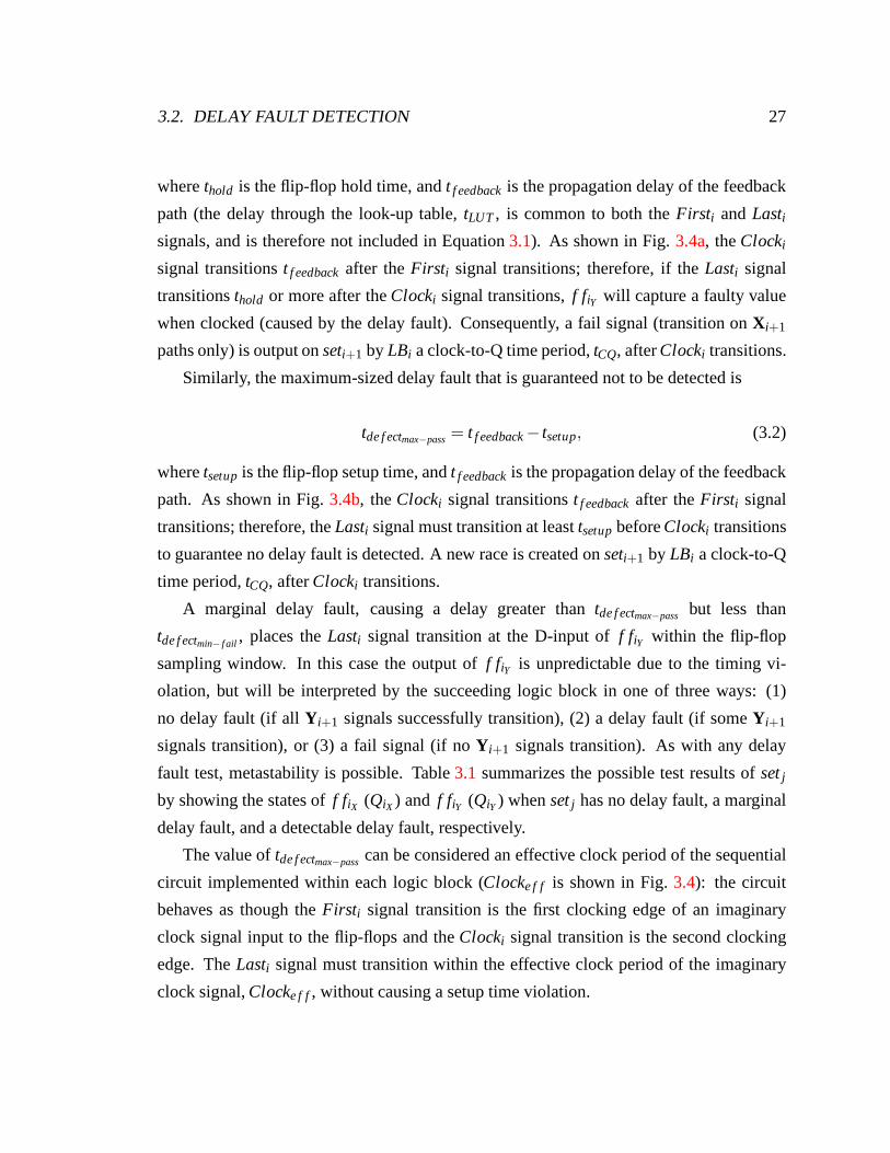
3.2. DELAY FAULT DETECTION 27
wherethold is the flip-flop hold time, andt f eedbackis the propagation delay of the feedback
path (the delay through the look-up table,tLUT , is common to both theFirsti andLasti
signals, and is therefore not included in Equation3.1). As shown in Fig.3.4a, theClocki
signal transitionst f eedbackafter theFirsti signal transitions; therefore, if theLasti signal
transitionsthold or more after theClocki signal transitions,f fiY will capture a faulty value
when clocked (caused by the delay fault). Consequently, a fail signal (transition onX i+1
paths only) is output onseti+1 by LBi a clock-to-Q time period,tCQ, afterClocki transitions.
Similarly, the maximum-sized delay fault that is guaranteed not to be detected is
tde f ectmax−pass= t f eedback− tsetup, (3.2)
wheretsetupis the flip-flop setup time, andt f eedbackis the propagation delay of the feedback
path. As shown in Fig.3.4b, theClocki signal transitionst f eedbackafter theFirsti signal
transitions; therefore, theLasti signal must transition at leasttsetupbeforeClocki transitions
to guarantee no delay fault is detected. A new race is createdonseti+1 by LBi a clock-to-Q
time period,tCQ, afterClocki transitions.
A marginal delay fault, causing a delay greater thantde f ectmax−pass but less than
tde f ectmin− f ail , places theLasti signal transition at the D-input off fiY within the flip-flop
sampling window. In this case the output off fiY is unpredictable due to the timing vi-
olation, but will be interpreted by the succeeding logic block in one of three ways: (1)
no delay fault (if allY i+1 signals successfully transition), (2) a delay fault (if some Y i+1
signals transition), or (3) a fail signal (if noY i+1 signals transition). As with any delay
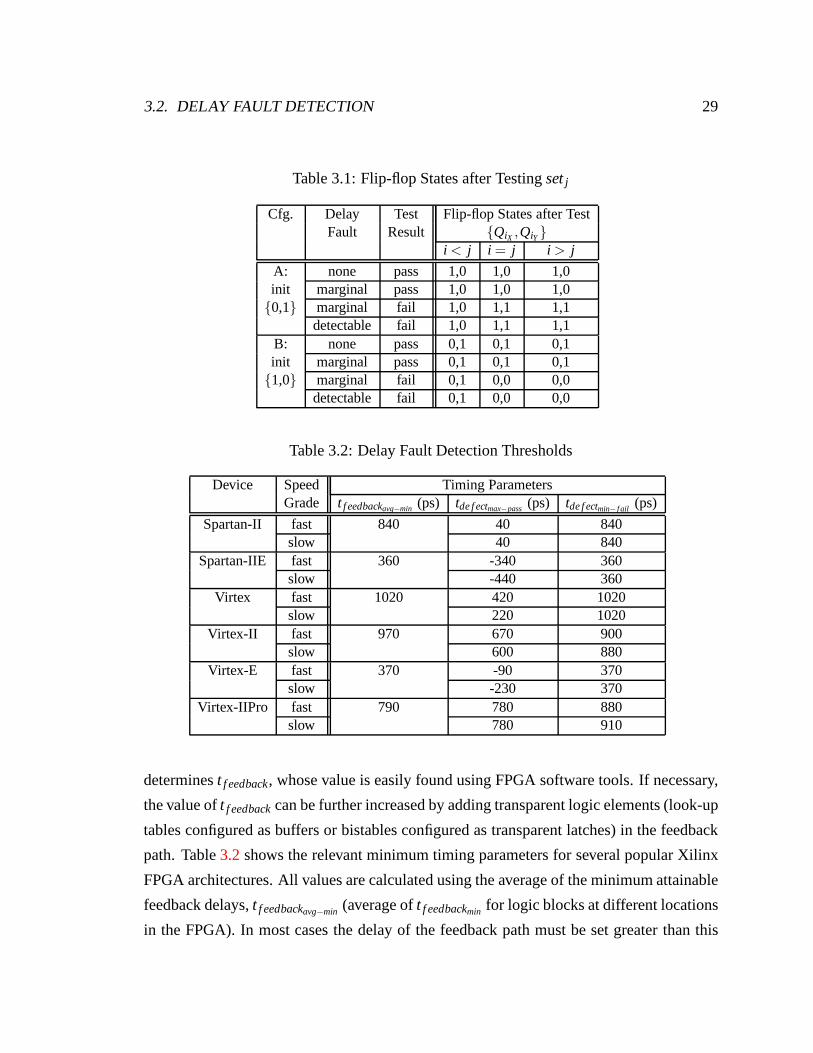
fault test, metastability is possible. Table3.1 summarizes the possible test results ofsetj
by showing the states off fiX (QiX ) and f fiY (QiY) whensetj has no delay fault, a marginal
delay fault, and a detectable delay fault, respectively.
The value oftde f ectmax−pass can be considered an effective clock period of the sequential
circuit implemented within each logic block (Clocke f f is shown in Fig.3.4): the circuit
behaves as though theFirsti signal transition is the first clocking edge of an imaginary
clock signal input to the flip-flops and theClocki signal transition is the second clocking
edge. TheLasti signal must transition within the effective clock period ofthe imaginary
clock signal,Clocke f f, without causing a setup time violation.
28 CHAPTER 3. DELAY FAULT TEST
First i
Last i
Clocki
t setupt defectmax−pass
Xi 1
Yi 1
Xi+11
Yi+11
Clockeff
t LUT
t defectmin−fail
t defect
t feedback
t hold
tCQ
* * * * * * * * * * * * ** * * * * * * * * * * * *+ + + + + + + + + + + + ++ + + + + + + + + + + + +
, , , , , ,, , , , , ,, , , , , ,, , , , , ,, , , , , ,, , , , , ,, , , , , ,, , , , , ,, , , , , ,, , , , , ,, , , , , ,, , , , , ,, , , , , ,
- - - - - -- - - - - -- - - - - -- - - - - -- - - - - -- - - - - -- - - - - -- - - - - -- - - - - -- - - - - -- - - - - -- - - - - -- - - - - -. . . . . . . . . . . . .. . . . . . . . . . . . ./ / / / / / / / / / / / // / / / / / / / / / / / /
1
0
1
1
fail
(a) Detectable Delay Fault inseti (fail)
First i
Clocki
t defectmax−pass
Xi 1
Yi 1
Last i
Yi+11
Xi+11
Clockeff
t LUT t feedback
t setup t hold
t CQ
tdefect
t defectmin−fail
0 0 0 0 0 00 0 0 0 0 00 0 0 0 0 00 0 0 0 0 00 0 0 0 0 00 0 0 0 0 00 0 0 0 0 00 0 0 0 0 00 0 0 0 0 00 0 0 0 0 00 0 0 0 0 00 0 0 0 0 00 0 0 0 0 0
1 1 1 1 1 11 1 1 1 1 11 1 1 1 1 11 1 1 1 1 11 1 1 1 1 11 1 1 1 1 11 1 1 1 1 11 1 1 1 1 11 1 1 1 1 11 1 1 1 1 11 1 1 1 1 11 1 1 1 1 11 1 1 1 1 12 2 2 22 2 2 2
3 3 33 3 3
4 4 44 4 45 5 55 5 5
0
1
1
0
pas
s
(b) No Delay Fault inseti (pass)
Figure 3.4: ConfigurationA Waveforms
The feedback delay (Firsti toClocki delay) can be adjusted to obtain an arbitrary effec-
tive clock period, and thus an arbitrary delay fault detection sensitivity (size of detectable
delay faults). The length of the feedback path (path throughthe interconnection network)
3.2. DELAY FAULT DETECTION 29
Table 3.1: Flip-flop States after Testingsetj
Cfg. Delay Test Flip-flop States after TestFault Result QiX ,QiY
i < j i = j i > j
A: none pass 1,0 1,0 1,0init marginal pass 1,0 1,0 1,00,1 marginal fail 1,0 1,1 1,1
detectable fail 1,0 1,1 1,1B: none pass 0,1 0,1 0,1init marginal pass 0,1 0,1 0,11,0 marginal fail 0,1 0,0 0,0
detectable fail 0,1 0,0 0,0
Table 3.2: Delay Fault Detection Thresholds
Device Speed Timing ParametersGrade t f eedbackavg−min (ps) tde f ectmax−pass (ps) tde f ectmin− f ail (ps)
Spartan-II fast 840 40 840slow 40 840
Spartan-IIE fast 360 -340 360slow -440 360
Virtex fast 1020 420 1020slow 220 1020
Virtex-II fast 970 670 900slow 600 880
Virtex-E fast 370 -90 370slow -230 370
Virtex-IIPro fast 790 780 880slow 780 910
determinest f eedback, whose value is easily found using FPGA software tools. If necessary,
the value oft f eedbackcan be further increased by adding transparent logic elements (look-up
tables configured as buffers or bistables configured as transparent latches) in the feedback
path. Table3.2shows the relevant minimum timing parameters for several popular Xilinx
FPGA architectures. All values are calculated using the average of the minimum attainable
feedback delays,t f eedbackavg−min (average oft f eedbackmin for logic blocks at different locations
in the FPGA). In most cases the delay of the feedback path mustbe set greater than this
30 CHAPTER 3. DELAY FAULT TEST
minimum to meet the setup time requirement for fault-free devices (so fault-free devices
are not erroneously failed), especially whentde f ectmax−pass< 0. Note that if the outputs of the
two flip-flops in a given logic block are not in close proximity(for example if the flip-flops
are physically the on opposite sides of the logic block), an additional timing margin must
be provided in the feedback path to account for the resultinginherent fault-free propagation
delay difference. The presented delay fault test is independent of both device architecture
and manufacturer: the relevant timing parameters are shownonly for Xilinx devices due to
our access to Xilinx FPGA software tools.
3.2.4 Resistive Opens
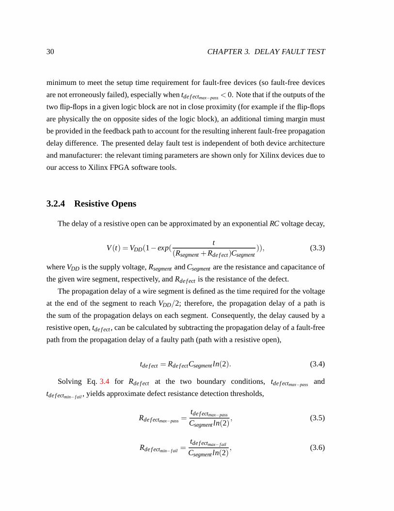
The delay of a resistive open can be approximated by an exponential RCvoltage decay,
V(t) = VDD(1−exp(t
(Rsegment+Rde f ect)Csegment)), (3.3)
whereVDD is the supply voltage,RsegmentandCsegmentare the resistance and capacitance of
the given wire segment, respectively, andRde f ect is the resistance of the defect.
The propagation delay of a wire segment is defined as the time required for the voltage
at the end of the segment to reachVDD/2; therefore, the propagation delay of a path is
the sum of the propagation delays on each segment. Consequently, the delay caused by a
resistive open,tde f ect, can be calculated by subtracting the propagation delay of afault-free
path from the propagation delay of a faulty path (path with a resistive open),
tde f ect= Rde f ectCsegmentln(2). (3.4)
Solving Eq.3.4 for Rde f ect at the two boundary conditions,tde f ectmax−pass and
tde f ectmin− f ail , yields approximate defect resistance detection thresholds,
Rde f ectmax−pass=tde f ectmax−pass
Csegmentln(2), (3.5)
Rde f ectmin− f ail =tde f ectmax− f ail
Csegmentln(2), (3.6)
3.2. DELAY FAULT DETECTION 31
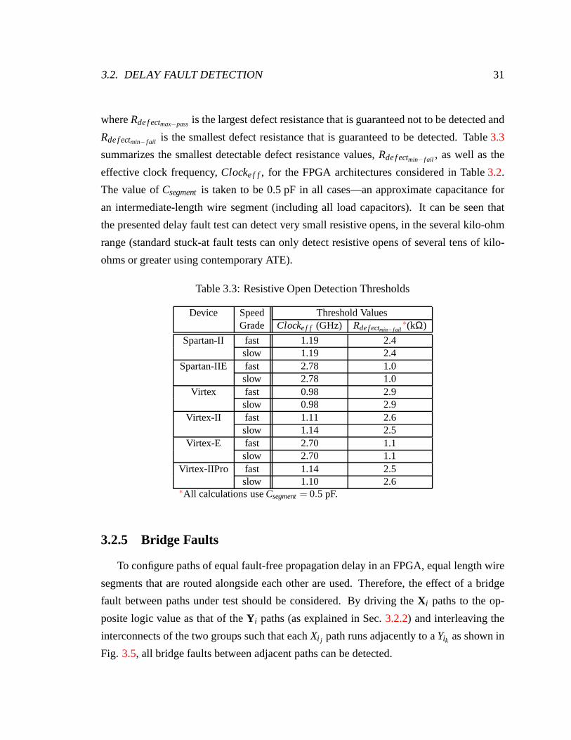
whereRde f ectmax−pass is the largest defect resistance that is guaranteed not to bedetected and
Rde f ectmin− f ail is the smallest defect resistance that is guaranteed to be detected. Table3.3
summarizes the smallest detectable defect resistance values,Rde f ectmin− f ail , as well as the
effective clock frequency,Clocke f f, for the FPGA architectures considered in Table3.2.
The value ofCsegmentis taken to be 0.5 pF in all cases—an approximate capacitancefor
an intermediate-length wire segment (including all load capacitors). It can be seen that
the presented delay fault test can detect very small resistive opens, in the several kilo-ohm
range (standard stuck-at fault tests can only detect resistive opens of several tens of kilo-
ohms or greater using contemporary ATE).
Table 3.3: Resistive Open Detection Thresholds
Device Speed Threshold ValuesGrade Clocke f f (GHz) Rde f ectmin− f ail
∗(kΩ)
Spartan-II fast 1.19 2.4slow 1.19 2.4
Spartan-IIE fast 2.78 1.0slow 2.78 1.0
Virtex fast 0.98 2.9slow 0.98 2.9
Virtex-II fast 1.11 2.6slow 1.14 2.5
Virtex-E fast 2.70 1.1slow 2.70 1.1
Virtex-IIPro fast 1.14 2.5slow 1.10 2.6
∗All calculations useCsegment= 0.5 pF.
3.2.5 Bridge Faults
To configure paths of equal fault-free propagation delay in an FPGA, equal length wire
segments that are routed alongside each other are used. Therefore, the effect of a bridge
fault between paths under test should be considered. By driving theX i paths to the op-
posite logic value as that of theY i paths (as explained in Sec.3.2.2) and interleaving the
interconnects of the two groups such that eachXi j path runs adjacently to aYik as shown in
Fig. 3.5, all bridge faults between adjacent paths can be detected.
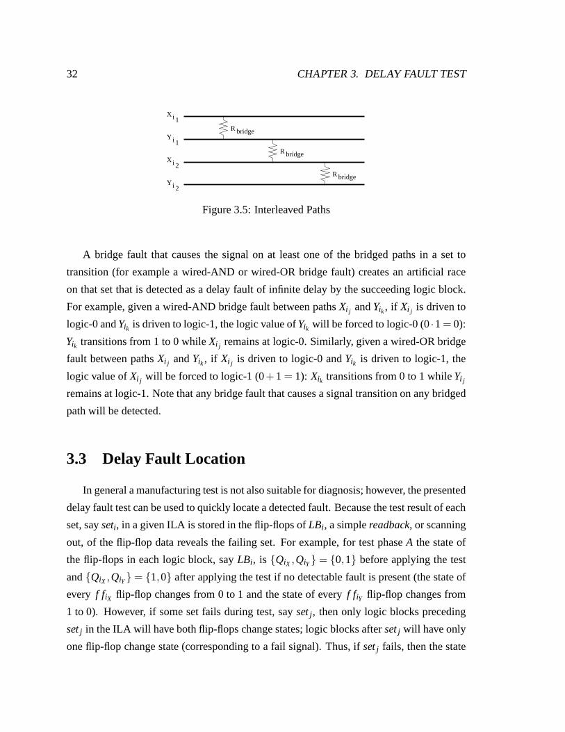
32 CHAPTER 3. DELAY FAULT TEST
Y i 1
X i 1
2X i
Y i 2
Rbridge
Rbridge
Rbridge
Figure 3.5: Interleaved Paths
A bridge fault that causes the signal on at least one of the bridged paths in a set to
transition (for example a wired-AND or wired-OR bridge fault) creates an artificial race
on that set that is detected as a delay fault of infinite delay by the succeeding logic block.
For example, given a wired-AND bridge fault between pathsXi j andYik, if Xi j is driven to
logic-0 andYik is driven to logic-1, the logic value ofYik will be forced to logic-0 (0·1= 0):
Yik transitions from 1 to 0 whileXi j remains at logic-0. Similarly, given a wired-OR bridge
fault between pathsXi j andYik, if Xi j is driven to logic-0 andYik is driven to logic-1, the
logic value ofXi j will be forced to logic-1 (0+1 = 1): Xik transitions from 0 to 1 whileYi j
remains at logic-1. Note that any bridge fault that causes a signal transition on any bridged
path will be detected.
3.3 Delay Fault Location
In general a manufacturing test is not also suitable for diagnosis; however, the presented
delay fault test can be used to quickly locate a detected fault. Because the test result of each
set, sayseti, in a given ILA is stored in the flip-flops ofLBi , a simplereadback, or scanning
out, of the flip-flop data reveals the failing set. For example, for test phaseA the state of
the flip-flops in each logic block, sayLBi , is QiX ,QiY = 0,1 before applying the test
andQiX ,QiY = 1,0 after applying the test if no detectable fault is present (the state of
every f fiX flip-flop changes from 0 to 1 and the state of everyf fiY flip-flop changes from
1 to 0). However, if some set fails during test, saysetj , then only logic blocks preceding
setj in the ILA will have both flip-flops change states; logic blocks aftersetj will have only
one flip-flop change state (corresponding to a fail signal). Thus, ifsetj fails, then the state
3.4. SUMMARY 33
of the flip-flops forLBi< j will be QiX ,QiY = 1,0 while the state of the flip-flops for
LBi≥ j will be QiX ,QiY = 1,1. Consequently, using readback to identify the first logic
block in an ILA in which both flip-flops have not changed state is sufficient to locate the
failing set.
3.4 Summary
Detecting delay faults is important for two reasons: (1) a delay fault can cause timing
failures, and (2) the defect that causes a delay fault, for example a resistive open, may result
in an early-life failure. The presented delay fault test candetect very small delay faults
(nanosecond range) without the need for high speed and expensive ATE. Additionally, the
ILA-based test configurations, which scale with FPGA size, permit fast fault location using
the readback capability of contemporary FPGAs.

34 CHAPTER 3. DELAY FAULT TEST
This page intentionally left blank.
Chapter 4
Bridge Fault Test
4.1 Motivation and Previous Work
A common failure mode of abridge fault—an undesired connection between circuit
nodes (interconnects, gate inputs, and gate outputs)—is the presence of a fault current,
which results when the bridged nodes are driven to opposite logic values (fault isactivated).
IDDQ, the total current drawn by a device in steady state, can be used to detect such a fault
current. StandardIDDQ test (single threshold) involves applying several test vectors to a
device under test, each activating potential bridge faultsin the device. For each test vector
an IDDQ value is measured (after transients settle). If any measurement is greater than a
predetermined threshold, the device is rejected [Horning et al. 1987] [Hawkins et al. 1989]
[Gulati and Hawkins 1992] [Rajsuman 1994] [Chakravarty and Thadikaran 1997].
IDDQ test is important for FPGAs due to the transmission-gate multiplexer im-
plementation of switch matrices [Xilinx, Inc. 2002a], in which some defects—shorts
to power or ground and stuck-on transistors—can only be detected via IDDQ test
[Makar and McCluskey 1996]. However, standardIDDQ test effectiveness has diminished
due to the dramatic increase in leakage currents of deep sub-micron devices: decreased
threshold voltages and increased transistor counts have caused an exponential increase in
IDDQ but have not caused a corresponding increase in fault currents. TheIDDQ of an FPGA
(leakage current) is especially high due to (1) the large interconnection network (large num-
ber of PIPs), and (2) the driving of unused interconnects to afixed logic value to reduce
noise and crosstalk (the unused portion of an FPGA contributes significant leakage). Recent
35
36 CHAPTER 4. BRIDGE FAULT TEST
studies have found that roughly 65% of total power dissipation is associated with the inter-
connection network [Kusse 1997] [Shang et al. 2002] [Poon et al. 2002] [Li et al. 2003].
Several techniques have been proposed to overcome this scaling limitation of standardIDDQ
test, although all are intended for non-configurable circuits like ASICs or microprocessors.
∆IDDQ test employs the discrete first derivative ofIDDQ as a function of vector number,
i, to detect a fault,∆IDDQi = IDDQi − IDDQi−1 (difference in successiveIDDQ measurements)
[Thibeault 1999] [Miller 1999] [Powell et al. 2000]. Because the difference between suc-
cessive pairs ofIDDQ measurements is used, vector order is very important for fault de-
tection. In contrast, current signature analysis places norestriction on vector order:IDDQ
values are measured for each test vector and then ordered based on magnitude (plotted on
a graph), called theIDDQ signature. A discontinuity in this signature (step) indicates some
short, perhaps a bridge fault, is present [Gattiker and Maly 1996] [Gattiker et al. 1996]. Fi-
nally, the current ratio method uses the ratio of the maximumand minimumIDDQ measure-
ments instead of comparing the absolute value ofIDDQ measurements. A dynamic threshold
is calculated based on the magnitude of the smallestIDDQ value (firstIDDQ measured); if
any subsequentIDDQ measurement is greater than this calculated threshold, thedevice is re-
jected [Maxwell et al. 2000]. In each method an attempt is made to reduce the large device
leakage current when detecting a much smaller fault current. However, because all circuit
nodes of an ASIC cannot be independently controlled (there is non-configurable logic and
inversion), a significant amount of leakage current is stillpresent.
4.2 Differential IDDQ Test
4.2.1 Overview
The presented bridge fault test utilizes the configurability of an FPGA to overcome the
limitations of the previous methods. Since the logic value of every circuit node can be
independently controlled by configuration (discussed in Sec. 4.2.2), a very effective bridge
fault test technique called differentialIDDQ test can be implemented. Detecting bridge
faults is important since they model the majority of defects[Fantini and Morandi 1985]
4.2. DIFFERENTIALIDDQ TEST 37
[Ferguson and Larrabee 1991]. Furthermore, because the interconnection network consti-
tutes the majority of an FPGA and due to the high density of thephysical layout in deep
sub-micron process technologies, interconnect bridge faults are an important concern.
To activate possible interconnect bridge faults in an FPGA,the logic value of each
interconnect is set by test configurations (device configurations) rather than test vectors
(each test configuration sets the logic value of a subset of the interconnects to the opposite
logic value as that of the rest). First, the device is configured such that all interconnects are
driven to the same logic value, say logic-1, and a reference current,IDDQre f , is measured.
Since no bridge faults are activated, the reference currentis simply the background leakage
current, for example the sum of all source-to-substrate leakage, sub-threshold drain current,
and gate leakage that is present when all circuit nodes are driven to logic-1. Next, the device
is reconfigured a number of times, each time setting a different subset of the interconnects
to the opposite logic value as that of the rest, say logic-0 (the number of configurations and
subsets of interconnects is discussed in Sec.4.2.2). For each configuration, a total current,
IDDQtot, is measured. Since any bridge fault between any interconnect driven to logic-0
and any driven to logic-1 is activated, each total current includes a possible fault current,
IDDQ f ault , an interconnect leakage current between the opposite-valued interconnects (state-
dependent leakage current),IDDQint , and the original background leakage current,IDDQre f .
As shown in Eq.4.1, the reference current (measured only once during the test of a
device) is subtracted from each total current, yielding a number of signature currents,
IDDQsig, each of which contains only the small interconnect leakagecurrent (leakage be-
tween opposite-valued interconnects),IDDQint , and the possible fault current,IDDQ f ault ,
IDDQsig = IDDQtot − IDDQre f
= (IDDQre f + IDDQint + IDDQ f ault)− IDDQre f
= IDDQint + IDDQ f ault .
(4.1)
Thus, by cancelling the large background leakage current, it is much easier to detect a
small fault current. However, because the difference in twomeasurements is used, which
theoretically doubles the variance, it is not possible to detect arbitrarily small fault currents.
Table4.1summarizes the variousIDDQ currents of the presented differentialIDDQ test.
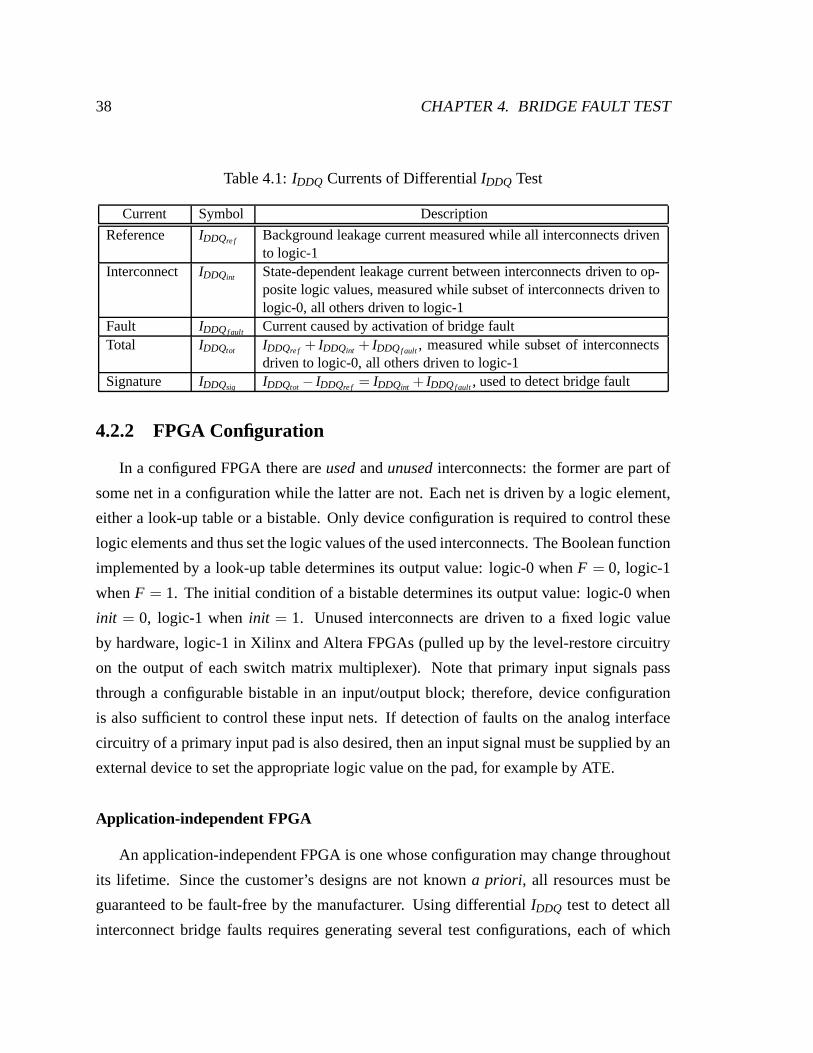
38 CHAPTER 4. BRIDGE FAULT TEST
Table 4.1:IDDQ Currents of DifferentialIDDQ Test
Current Symbol Description
Reference IDDQre f Background leakage current measured while all interconnects drivento logic-1
Interconnect IDDQint State-dependent leakage current between interconnects driven to op-posite logic values, measured while subset of interconnects driven tologic-0, all others driven to logic-1
Fault IDDQf ault Current caused by activation of bridge faultTotal IDDQtot IDDQre f + IDDQint + IDDQf ault, measured while subset of interconnects
driven to logic-0, all others driven to logic-1Signature IDDQsig IDDQtot − IDDQre f = IDDQint + IDDQf ault, used to detect bridge fault
4.2.2 FPGA Configuration
In a configured FPGA there areusedandunusedinterconnects: the former are part of
some net in a configuration while the latter are not. Each net is driven by a logic element,
either a look-up table or a bistable. Only device configuration is required to control these
logic elements and thus set the logic values of the used interconnects. The Boolean function
implemented by a look-up table determines its output value:logic-0 whenF = 0, logic-1
whenF = 1. The initial condition of a bistable determines its outputvalue: logic-0 when
init = 0, logic-1 wheninit = 1. Unused interconnects are driven to a fixed logic value
by hardware, logic-1 in Xilinx and Altera FPGAs (pulled up bythe level-restore circuitry
on the output of each switch matrix multiplexer). Note that primary input signals pass
through a configurable bistable in an input/output block; therefore, device configuration
is also sufficient to control these input nets. If detection of faults on the analog interface
circuitry of a primary input pad is also desired, then an input signal must be supplied by an
external device to set the appropriate logic value on the pad, for example by ATE.
Application-independent FPGA
An application-independent FPGA is one whose configurationmay change throughout
its lifetime. Since the customer’s designs are not knowna priori, all resources must be
guaranteed to be fault-free by the manufacturer. Using differentialIDDQ test to detect all
interconnect bridge faults requires generating several test configurations, each of which
4.2. DIFFERENTIALIDDQ TEST 39
drives a set of adjacent interconnects to opposite logic values. In each configuration the
used interconnects are driven to logic-0, activating any bridge fault to any unused inter-
connect (logic-1). Figure4.1 shows the per test configuration steps to test an FPGA via
differentialIDDQ. Steps 1 and 2 can be interchanged with steps 3 and 4, respectively.
1. Configure FPGA to drive all interconnects to logic-1
2. Measure reference current,IDDQre f
3. Configure FPGA to drive subset of interconnects to logic-0andall others to logic-1
4. Measure total current,IDDQtot
5. Determine signature current,IDDQsig = IDDQtot − IDDQre f
6. Is IDDQsig > threshold?
(a) Yes, device fails configuration(b) No, device passes configuration
Figure 4.1: Per Test Configuration Test Flow
Minimizing the number of configurations, and thus the numberof IDDQ measurements,
to detect all interconnect bridge faults is paramount to reducing test time, since it takes
roughly 4–8 ms to configure a Xilinx Virtex-II FPGA (other architectures have similar
configuration times, which is dependent on FPGA size) and nearly 20 ms for contemporary
ATE to measure theIDDQ. Although there are thousands of interconnects in an FPGA,
the tiled layout and bus-oriented (grouped) interconnection network can be exploited to
minimize the number of configurations needed to test for all single and most multiple bridge
faults between adjacent interconnects.
For a Virtex-II FPGA with 8 metal layers [Xilinx, Inc. 2002a], in which each intercon-
nect type (horizontal long, vertical long, horizontal hex,vertical hex, horizontal double,
vertical double, direct, and fast) is routed primarily within a single layer, only 5 test con-
figurations are required to detect all pairwise interconnect bridge faults (bridges between
adjacent interconnects), accomplished by interleaving interconnects [Chmelar 2003]. In-
terleaving, or driving every other interconnect of a particular type tologic-0 while the
remainder are driven to logic-1, activates all bridge faults between adjacent interconnects
within a metal layer, and thus permits fault detection givena resulting fault current. By
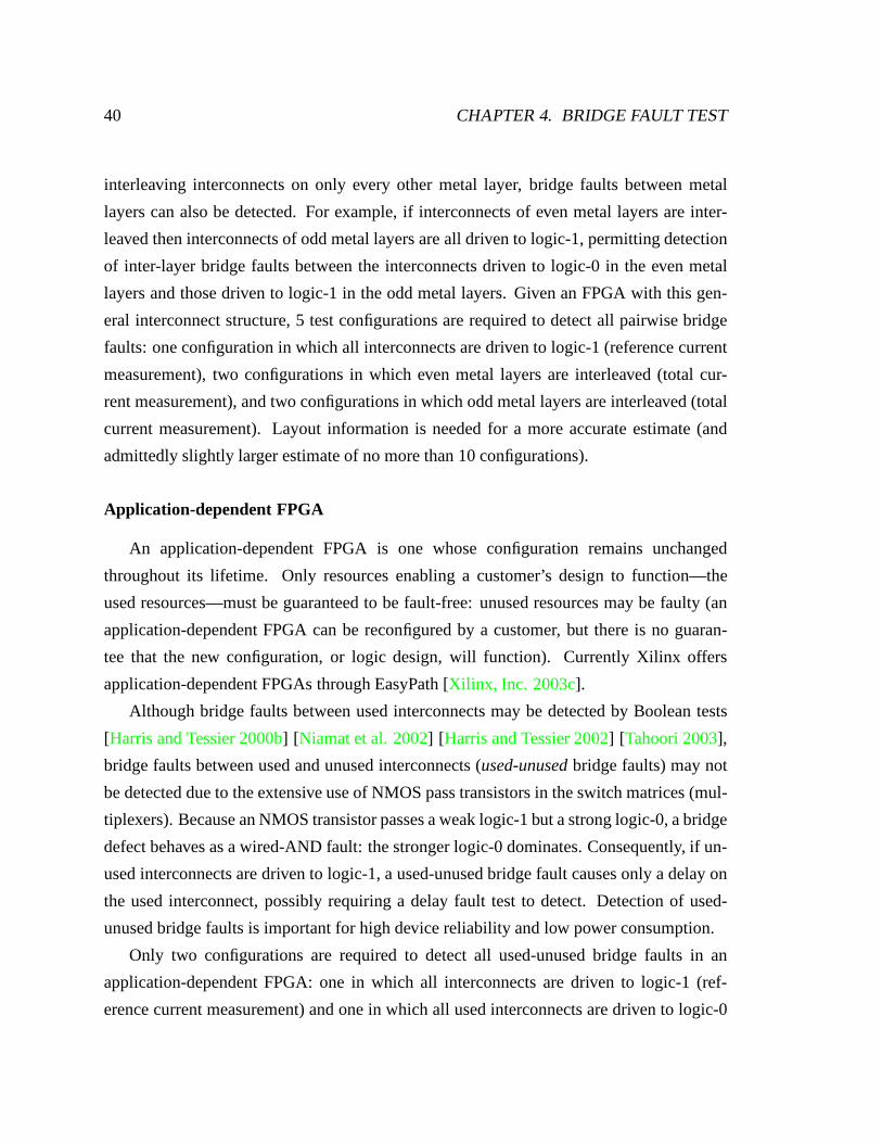
40 CHAPTER 4. BRIDGE FAULT TEST
interleaving interconnects on only every other metal layer, bridge faults between metal
layers can also be detected. For example, if interconnects of even metal layers are inter-
leaved then interconnects of odd metal layers are all drivento logic-1, permitting detection
of inter-layer bridge faults between the interconnects driven to logic-0 in the even metal
layers and those driven to logic-1 in the odd metal layers. Given an FPGA with this gen-
eral interconnect structure, 5 test configurations are required to detect all pairwise bridge
faults: one configuration in which all interconnects are driven to logic-1 (reference current
measurement), two configurations in which even metal layersare interleaved (total cur-
rent measurement), and two configurations in which odd metallayers are interleaved (total
current measurement). Layout information is needed for a more accurate estimate (and
admittedly slightly larger estimate of no more than 10 configurations).
Application-dependent FPGA
An application-dependent FPGA is one whose configuration remains unchanged
throughout its lifetime. Only resources enabling a customer’s design to function—the
used resources—must be guaranteed to be fault-free: unusedresources may be faulty (an
application-dependent FPGA can be reconfigured by a customer, but there is no guaran-
tee that the new configuration, or logic design, will function). Currently Xilinx offers
application-dependent FPGAs through EasyPath [Xilinx, Inc. 2003c].
Although bridge faults between used interconnects may be detected by Boolean tests
[Harris and Tessier 2000b] [Niamat et al. 2002] [Harris and Tessier 2002] [Tahoori 2003],
bridge faults between used and unused interconnects (used-unusedbridge faults) may not
be detected due to the extensive use of NMOS pass transistorsin the switch matrices (mul-
tiplexers). Because an NMOS transistor passes a weak logic-1 but a strong logic-0, a bridge
defect behaves as a wired-AND fault: the stronger logic-0 dominates. Consequently, if un-
used interconnects are driven to logic-1, a used-unused bridge fault causes only a delay on
the used interconnect, possibly requiring a delay fault test to detect. Detection of used-
unused bridge faults is important for high device reliability and low power consumption.
Only two configurations are required to detect all used-unused bridge faults in an
application-dependent FPGA: one in which all interconnects are driven to logic-1 (ref-
erence current measurement) and one in which all used interconnects are driven to logic-0
4.2. DIFFERENTIALIDDQ TEST 41
(total current measurement). To drive all used interconnects to logic-0, all used look-up
tables (used in the customer’s design) are configured to implement the functionF = 0 and
all used bistables are configured with the initial conditioninit = 0; routing of nets remains
unchanged. Note that the logic value on a net that is theset/reset input to a bistable (a
used element) can cause the output of that bistable (anothernet) to be different than the
initial value to which it was initialized. For example, to activate possible bridge faults, all
nets are driven to logic-0. Consider some bistable whose output is initialized to logic-0;
if the bistable has an active-lowset/reset input, which is by definition also driven to
logic-0, then its output will change from logic-0 (initialized value) to logic-1 (caused by
set/reset). Therefore, to prevent theset/reset input from affecting the output of a
bistable, it must be made active-high or synchronous, or disconnected.
4.2.3 Experimental Results
Bridge fault emulation [Toutounchi et al. 2003] was used to conduct experiments on 5
randomly chosen Xilinx Spartan-3 XC3S50 devices, each manufactured in a 90 nm pro-
cess. An unused PIP joining a used and unused interconnect was programmed to be on,
emulating a bridge defect of roughly 1 kΩ or a stuck-on PIP. Figure4.2ashows a PIP and
its associated SRAM cell (a stored logic-0 indicates the PIPis off; a stored logic-1 indicates
the PIP is on), Fig.4.2bshows a PIP in the off state and a real bridge defect, and Fig.4.2c
shows a PIP in the on state emulating a bridge defect. The benefit of using bridge fault emu-
lation for the experiments is that the resulting fault current can be easily determined simply
by subtracting theIDDQ measurement obtained when the fault is not emulated (fault-free
case) from the measurement obtained when the fault is emulated (faulty case).
M
(a) PIP Joining Interconnects
0
(b) Real Bridge Defect
1
(c) Emulated Bridge Defect
Figure 4.2: Bridge Fault Emulation
42 CHAPTER 4. BRIDGE FAULT TEST
The detectabilityof a fault current is a measure of how large it is with respect to the
IDDQ magnitude: a larger detectability means the fault current is more easily detected. In
standardIDDQ test, the detectability,ds, is the ratio of the fault current,IDDQ f ault , and the
total current,IDDQtot,
ds =IDDQ f ault
IDDQtot
. (4.2)
In differential IDDQ test, the detectability,dd, becomes the ratio of the fault current,
IDDQ f ault , and the signature current,IDDQsig,
dd =IDDQ f ault
IDDQsig
. (4.3)
Finally, theimprovement, i, of differentialIDDQ test over standardIDDQ test is the ratio
of the detectabilities of the two methods,dd andds,
i =dd
ds=
IDDQtot
IDDQsig
. (4.4)
Table4.2shows theIDDQ values for each of the 5 Spartan-3 devices, each programmed
with the same very dense configuration that uses 3.66% of all PIPs. It can be seen that stan-
dardIDDQ test yields detectability ratios of approximately 0.13, meaning the fault current
constitutes only 13% of theIDDQ value that is compared to the threshold. In contrast, differ-
ential IDDQ test yields detectability ratios of approximately 0.65, meaning the fault current
constitutes 65% of theIDDQ value that is compared to the threshold. This difference results
in an improvement ratio of approximately 5, meaning it is roughly 5 times easier to detect
the same bridge fault using differentialIDDQ test than it is using standardIDDQ test.
The data of Table4.2 shows another advantage of differentialIDDQ test: it is much
easier to determine agood threshold—one that passes fault-free devices and fails faulty
devices—for differentialIDDQ test than it is for standardIDDQ test. It can be seen that the
fault-free total current of device 4 is greater than the faulty total current of devices 3 and
5, making it impossible to determine a good threshold for standardIDDQ test. For example,
if the threshold were set to 2.0 mA, device 4 would fail when fault-free (false failure) and
device 3 would pass when faulty (test escape), shown in Fig.4.3a. However, if differential
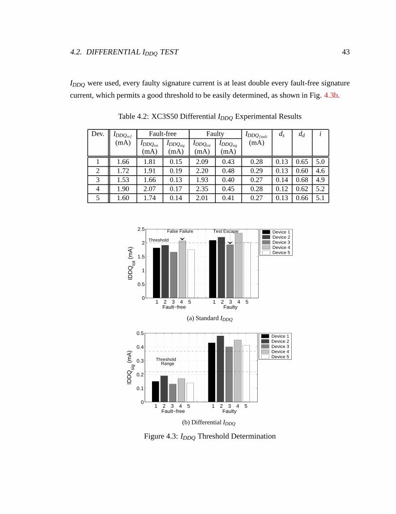
4.2. DIFFERENTIALIDDQ TEST 43
IDDQ were used, every faulty signature current is at least doubleevery fault-free signature
current, which permits a good threshold to be easily determined, as shown in Fig.4.3b.
Table 4.2: XC3S50 DifferentialIDDQ Experimental Results
Dev. IDDQre f Fault-free Faulty IDDQf ault ds dd i(mA) IDDQtot IDDQsig IDDQtot IDDQsig (mA)
(mA) (mA) (mA) (mA)
1 1.66 1.81 0.15 2.09 0.43 0.28 0.13 0.65 5.02 1.72 1.91 0.19 2.20 0.48 0.29 0.13 0.60 4.63 1.53 1.66 0.13 1.93 0.40 0.27 0.14 0.68 4.94 1.90 2.07 0.17 2.35 0.45 0.28 0.12 0.62 5.25 1.60 1.74 0.14 2.01 0.41 0.27 0.13 0.66 5.1
Device 1Device 2Device 3Device 4Device 5
1 2 3 4 5 1 2 3 4 50
0.5
1
1.5
2
2.5
IDD
Qto
t (m
A)
Fault−free Faulty
Threshold
False Failure Test Escape
(a) StandardIDDQ
Device 1Device 2Device 3Device 4Device 5
1 2 3 4 5 1 2 3 4 50
0.1
0.2
0.3
0.4
0.5
IDD
Qsi
g (m
A)
Fault−free Faulty
ThresholdRange
(b) DifferentialIDDQ
Figure 4.3:IDDQ Threshold Determination
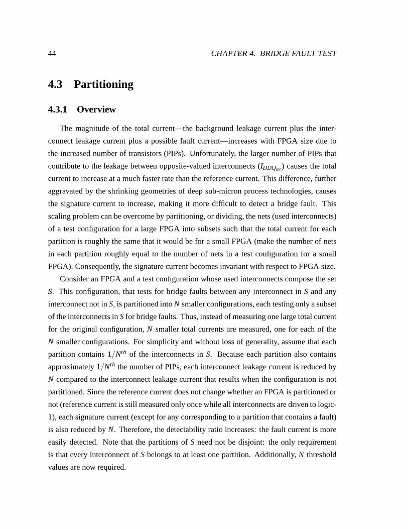
44 CHAPTER 4. BRIDGE FAULT TEST
4.3 Partitioning
4.3.1 Overview
The magnitude of the total current—the background leakage current plus the inter-
connect leakage current plus a possible fault current—increases with FPGA size due to
the increased number of transistors (PIPs). Unfortunately, the larger number of PIPs that
contribute to the leakage between opposite-valued interconnects (IDDQint ) causes the total
current to increase at a much faster rate than the reference current. This difference, further
aggravated by the shrinking geometries of deep sub-micron process technologies, causes
the signature current to increase, making it more difficult to detect a bridge fault. This
scaling problem can be overcome by partitioning, or dividing, the nets (used interconnects)
of a test configuration for a large FPGA into subsets such thatthe total current for each
partition is roughly the same that it would be for a small FPGA(make the number of nets
in each partition roughly equal to the number of nets in a testconfiguration for a small
FPGA). Consequently, the signature current becomes invariant with respect to FPGA size.
Consider an FPGA and a test configuration whose used interconnects compose the set
S. This configuration, that tests for bridge faults between any interconnect inS and any
interconnect not inS, is partitioned intoN smaller configurations, each testing only a subset
of the interconnects inSfor bridge faults. Thus, instead of measuring one large total current
for the original configuration,N smaller total currents are measured, one for each of the
N smaller configurations. For simplicity and without loss of generality, assume that each
partition contains 1/Nth of the interconnects inS. Because each partition also contains
approximately 1/Nth the number of PIPs, each interconnect leakage current is reduced by
N compared to the interconnect leakage current that results when the configuration is not
partitioned. Since the reference current does not change whether an FPGA is partitioned or
not (reference current is still measured only once while allinterconnects are driven to logic-
1), each signature current (except for any corresponding toa partition that contains a fault)
is also reduced byN. Therefore, the detectability ratio increases: the fault current is more
easily detected. Note that the partitions ofS need not be disjoint: the only requirement
is that every interconnect ofSbelongs to at least one partition. Additionally,N threshold
values are now required.
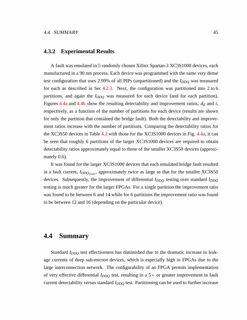
4.4. SUMMARY 45
4.3.2 Experimental Results
A fault was emulated in 5 randomly chosen Xilinx Spartan-3 XC3S1000 devices, each
manufactured in a 90 nm process. Each device was programmed with the same very dense
test configuration that uses 2.99% of all PIPs (unpartitioned) and theIDDQ was measured
for each as described in Sec4.2.3. Next, the configuration was partitioned into 2 to 6
partitions, and again theIDDQ was measured for each device (and for each partition).
Figures4.4aand4.4b show the resulting detectability and improvement ratios,dd and i,
respectively, as a function of the number of partitions for each device (results are shown
for only the partition that contained the bridge fault). Both the detectability and improve-
ment ratios increase with the number of partitions. Comparing the detectability ratios for
the XC3S50 devices in Table4.2with those for the XC3S1000 devices in Fig.4.4a, it can
be seen that roughly 6 partitions of the larger XC3S1000 devices are required to obtain
detectability ratios approximately equal to those of the smaller XC3S50 devices (approxi-
mately 0.6).
It was found for the larger XC3S1000 devices that each emulated bridge fault resulted
in a fault current,IDDQ f ault , approximately twice as large as that for the smaller XC3S50
devices. Subsequently, the improvement of differentialIDDQ testing over standardIDDQ
testing is much greater for the larger FPGAs. For a single partition the improvement ratio
was found to be between 6 and 14 while for 6 partitions the improvement ratio was found
to be between 12 and 16 (depending on the particular device).
4.4 Summary
StandardIDDQ test effectiveness has diminished due to the dramatic increase in leak-
age currents of deep sub-micron devices, which is especially high in FPGAs due to the
large interconnection network. The configurability of an FPGA permits implementation
of very effective differentialIDDQ test, resulting in a 5× or greater improvement in fault
current detectability versus standardIDDQ test. Partitioning can be used to further increase
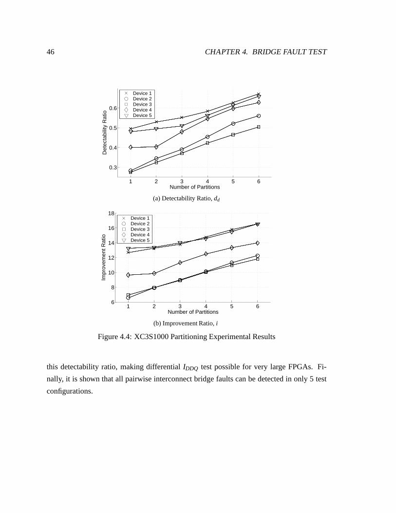
46 CHAPTER 4. BRIDGE FAULT TEST
1 2 3 4 5 6
0.3
0.4
0.5
0.6
Number of Partitions
Det
ecta
bilit
y R
atio
Device 1Device 2Device 3Device 4Device 5
(a) Detectability Ratio,dd
1 2 3 4 5 66
8
10
12
14
16
18
Number of Partitions
Impr
ovem
ent R
atio
Device 1Device 2Device 3Device 4Device 5
(b) Improvement Ratio,i
Figure 4.4: XC3S1000 Partitioning Experimental Results
this detectability ratio, making differentialIDDQ test possible for very large FPGAs. Fi-
nally, it is shown that all pairwise interconnect bridge faults can be detected in only 5 test
configurations.
Chapter 5
Test Time Reduction
5.1 Motivation and Previous Work
Testing an integrated circuit using ATE, for example an ASICor microprocessor, con-
sists of applying test vectors (input stimuli) and observing the responses. An additional
step is required when testing an FPGA: before test vectors are applied the device must be
programmed to implement some logic function. Because the manufacturer cannot know
which logic and routing resources of an application-independent FPGA will be used by a
customer, each of the literally billions of possible configurations must function. To main-
tain reasonable test time, only a small subset of these configurations can be tested. A
trade-off is made between the number of configurations tested (test configurations) and the
fault coverage (faults that can be detected).
Although each FPGA logic resource is configurable, its simplicity permits straightfor-
ward test: there are well-known techniques to test the logicresources [Stroud et al. 1996]
[Huang and Lombardi 1996] [Renovell and Zorian 2000]. In contrast, due to the large
number of signal paths that can be configured between a pair oflogic blocks or input/output
blocks (hundreds of paths), testing the interconnection network is very difficult: in practice
most of the several hundred test configurations used to test an FPGA target faults in the in-
terconnection network (this information was obtained through personal contacts at Xilinx,
Inc.). Therefore, the problem of reducing the long FPGA testtime is one of achieving high
fault coverage of the interconnection network in the shortest time possible.
FPGA test involves many iterations of: (1) program the device with a test configura-
tion, and (2) apply test vectors and observe the output responses. Because the time required
47
48 CHAPTER 5. TEST TIME REDUCTION
to program an FPGA—theconfiguration time—is several milliseconds while applying test
vectors and observing the responses takes several microseconds (see example calculation
in Sec.5.2.3), and because many configurations are needed to test all of the logic and rout-
ing resources, configuration time is the dominant part of test time [Doumar and Ito 1999]
[Toutounchi and Lai 2002]: data personally collected at Xilinx shows that over 90% ofthe
test time is spent programming the device while less than 10%is spent actually applying
test vectors and observing responses. Therefore, to significantly decrease the test time of
an FPGA, a reduction must be made in either (1) the number of test configurations, or (2)
the configuration time.
Several test configuration generation techniques have beenproposed to alleviate this
test time problem by reducing the number of test configurations. Although most tech-
niques consider only the fault coverage of the logic resources [Renovell et al. 1997b]
[Renovell et al. 1999a] [Renovell et al. 1999b], some do consider the fault coverage of the
interconnection network [Sun et al. 2002a] [Sun et al. 2002b] [Tahoori and Mitra 2003].
Those that consider faults in the interconnection network derive a reduced number of test
configurations using interconnect modeling and graph traversal algorithms.
Rather than reduce the number of test configurations, test time can be made shorter
by reducing the configuration time (time required to programan FPGA under test with
each test configuration). A modified configuration memory architecture is proposed in
[Doumar and Ito 1999] that allows internal shifting of test configuration data within an
FPGA, thereby reducing the number of test configurations that must be externally pro-
grammed into the device under test. However, it assumes the configuration memory is
structured as a single scan chain. Furthermore, the specially designed test configuration
that is internally shifted within an FPGA detects only faults in the logic resources.
5.2 FPGA Programming
5.2.1 Overview
The presented technique reduces the configuration time by taking advantage of the
tiled, or array-like, regularity of both an FPGA and its test configurations (discussed in
5.2. FPGA PROGRAMMING 49
Sec.5.2.3). A small amount ofDesign for Test(DFT) hardware (discussed in Sec.5.3) is
added to the existing configuration hardware to permit configuration data to be shifted into
theFrame Data Input Register(FDIR) in parallel (FDIR is defined in Sec.5.2.2). The ad-
vantages of this test time reduction technique, calledsubframe multiplex programming, are
(1) no modification to the configuration memory is required, and (2) faults in both the logic
resources and interconnection network can be detected since the existing manufacturing
test configurations, which achieve high fault coverage of both logic and routing resources,
are still used to test the FPGA.
5.2.2 Configuration Hardware
The configuration memory of an FPGA—a distributed array of SRAM cells selected
by vertical address lines and programmed via horizontal data lines—is programmed by
the configuration hardware. The smallest unit of memory thatcan be independently pro-
grammed, called aframe, is a 1-bit wide column of memory that spans allR rows of the
device (entire FPGA array height). Each column of logic block tiles (LB column) or in-
put/output block tiles (IOB column) contains 48 frames (48 frames wide) in a Virtex FPGA
[Xilinx, Inc. 2002b] [Xilinx, Inc. 2003b] (a tile is a logic block or input/output block and
its associated switch matrix). Figure5.1shows the organization of the configuration mem-
ory in an FPGA withR rows andC columns (R×C FPGA); frames are oriented vertically.
The configuration data of a single tile,N×P bits for a tile that isN bits tall andP bits
wide, is distributed across multiple frames (P frames). Each frame isR×N bits (R rows,
eachN bits tall), each containing only part of the configuration data for every tile in a
particular column. In the Virtex architecture, all tiles are 18 bits tall (N = 18) and 48 bits
wide (P = 48), yieldingN×P = 18×48= 864 configuration data bits per tile.
A frame of configuration data is written to the configuration memory from theFrame
Data Input Register(FDIR). The FDIR is a single-input scan chain spanning allR rows of
an FPGA: it stores exactly one frame of configuration data. Thus, programming an FPGA
with a complete configuration consists of many iterations of: (1) shift the configuration
data of a single frame into the FDIR, and (2) write the contents of the FDIR to a particular
address (frame location) in the configuration memory. Figure5.2shows a detailed diagram
50 CHAPTER 5. TEST TIME REDUCTION
IOB tile
(2,1)
IOB tile
(1,2)
IOB tile
(1,1)
LB tile
(2,2)
LB tile
(2,C−1)
IOB tile
(1,C)
LB tile
(R−1,2)
IOB tile
(R,1)
(R−1,C−1)
LB tile
IOB tile
(R,C)
IOB tile
(1,C−1)
IOB tile
(R−1,1)
IOB tile
(R,2)
IOB tile
(R,C−1)
IOB tile
(R−1,C)
IOB tile
(2,C)
rowR−1
rowR
row2
21fr
ame
fram
e1 1
fram
e1 P
fram
eC
1C
2fr
ame
fram
eC
P
bit1 2 row1
bit 1 1
bit 1 N
bitR 1bitR 2
bit R Nco
lum
nC
−1
colu
mn
C
colu
mn
1
colu
mn
2
FD
IR
Figure 5.1:R×C Tiled FPGA (frames shown vertically and FDIR on the left)
of the FDIR and the configuration memory. For simplicity and without loss of generality,
the FDIR is shown on the left side of the FPGA in Figs5.1and5.2 rather than its typical
central location.
5.2.3 Contemporary FPGA Programming Methods
Standard Programming
The configurationbitstreamis the data file used to program an FPGA, which contains
the configuration data as well as frame addressing, frame write control, frame padding, and
error correcting information. Because the non-configuration data information constitutes
only a small portion of the bitstream, it can be neglected when approximating the bitstream
size. Thus, given tiled FPGA withR rows andC columns, where each row isN configu-
ration bits tall and each column isP configuration bits wide (corresponding to a tile with
5.2. FPGA PROGRAMMING 51
bit 2N
bit 21
bit 1N
bit 11
M MM M M M MM
M MM M M M MM
decoder
address
DQQ
DQQ
DQQ
DQQ
M MM M M M MM
M MM M M M MM
IOB tile
(1,C−1)
IOB tile
(1,2)
IOB tile
(1,1)
IOB tile
(1,C)
LB tile
(2,C−1)
LB tile
(2,2)
LB tile
(R−1,2) (R−1,C−1)
LB tile
(2,1)
IOB tile
fram
e1 1
fram
e1 P
fram
eC
P
fram
eC
1
fram
eC
−1 P
fram
eC
−1 1
fram
e2
1
fram
e2
P
FD
IR
M MM M M M MM
M MM M M M MM
M MM M M M MM
M M M M M MM M
DQQ
DQQ
DQQ
DQQbit R N
bit R 1
bit R−1N
bit R−11
IOB tile
(R,1)
IOB tile
(R,C)
IOB tile
(R,2)
IOB tile
(R,C−1)
(R−1,1)
IOB tile
(2,C)
IOB tile
(R−1,C)
IOB tile
writecfg. data input
Figure 5.2: FDIR (left) and Configuration Memory (right)
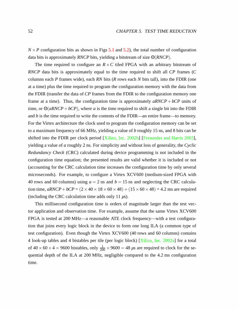
52 CHAPTER 5. TEST TIME REDUCTION
N×P configuration bits as shown in Figs5.1and5.2), the total number of configuration
data bits is approximatelyRNCPbits, yielding a bitstream of sizeΘ(RNCP).
The time required to configure anR×C tiled FPGA with an arbitrary bitstream of
RNCPdata bits is approximately equal to the time required to shift all CP frames (C
columns eachP frames wide), eachRN bits (R rows eachN bits tall), into the FDIR (one
at a time) plus the time required to program the configurationmemory with the data from
the FDIR (transfer the data ofCP frames from the FDIR to the configuration memory one
frame at a time). Thus, the configuration time is approximately aRNCP+bCP units of
time, orΘ(aRNCP+bCP), wherea is the time required to shift a single bit into the FDIR
andb is the time required to write the contents of the FDIR—an entire frame—to memory.
For the Virtex architecture the clock used to program the configuration memory can be set
to a maximum frequency of 66 MHz, yielding a value ofb roughly 15 ns, and 8 bits can be
shifted into the FDIR per clock period [Xilinx, Inc. 2002b] [Fernandes and Harris 2003],
yielding a value ofa roughly 2 ns. For simplicity and without loss of generality,theCyclic
Redundancy Check(CRC) calculated during device programming is not includedin the
configuration time equation; the presented results are valid whether it is included or not
(accounting for the CRC calculation time increases the configuration time by only several
microseconds). For example, to configure a Virtex XCV600 (medium-sized FPGA with
40 rows and 60 columns) usinga = 2 ns andb = 15 ns and neglecting the CRC calcula-
tion time,aRNCP+bCP= (2×40×18×60×48)+(15×60×48) = 4.2 ms are required
(including the CRC calculation time adds only 11µs).
This millisecond configuration time is orders of magnitude larger than the test vec-
tor application and observation time. For example, assume that the same Virtex XCV600
FPGA is tested at 200 MHz—a reasonable ATE clock frequency—with a test configura-
tion that joins every logic block in the device to form one long ILA (a common type of
test configuration). Even though the Virtex XCV600 (40 rows and 60 columns) contains
4 look-up tables and 4 bistables per tile (per logic block) [Xilinx, Inc. 2002a] for a total
of 40×60×4 = 9600 bistables, only1200×9600= 48µs are required to clock for the se-
quential depth of the ILA at 200 MHz, negligible compared to the 4.2 ms configuration
time.
5.2. FPGA PROGRAMMING 53
Multiframe Programming
The Θ(RNCP) bitstream size andΘ(aRNCP+bCP) configuration time for standard
FPGA programming result from arbitrary logic designs (typical customer designs) that
have little or no regularity. In contrast, manufacturing test configurations are highly regular
since they are usually generated based on the tiled architecture of an FPGA, which permits
the configurations to easily scale between device sizes. Twotechniques are commonly used
by FPGA manufacturers to generate test configurations, stamping and templating.Stamp-
ing is a process of manually creating a test configuration for a single tile and duplicating
that configuration across all similar tiles to generate a complete test configuration (for the
entire FPGA).Templatingis a process whereby a template, which determines the routing
resources (PIPs) to use in a particular path between a pair oflogic blocks (either within or
between tiles), is applied to all similar paths to generate acomplete test configuration. The
result of either technique is test configurations in which all similar FPGA columns have
identical configurations, for example all LB columns are identical.. Thus, thepth frame of
each identically configured column is identical, as shown inFigure5.3.
The duplication of configuration data (frames) between columns permits a method
called multiframe programming to be used (currently used inpractice). In multiframe
programming, only one instance of the data for each identical frame is included in the bit-
stream of a test configuration. This single frame is shifted into the FDIR once but written to
the configuration memory multiple times (multiple memory locations). The advantages of
multiframe programming, which applies to tiled test configurations, are that the bitstream
size is reduced toΘ(RNP) and the configuration time is reduced toΘ(aRNP+bCP).
Subframe Repeat Programming
Templating and stamping not only result in duplication of configuration data between
frames, but duplication within a single frame: in anR×C tiled FPGA where each row isN
configuration bits tall, each group ofN configuration bits of a particular frame is identical.
Therefore, the bitstream size can be significantly reduced by storing the uniqueN bits of a
frame, called asubframe, only once (a frame has a total ofRN bits).
Each LB column in an FPGA—the central columns in Fig.5.1—contains two IOB tiles
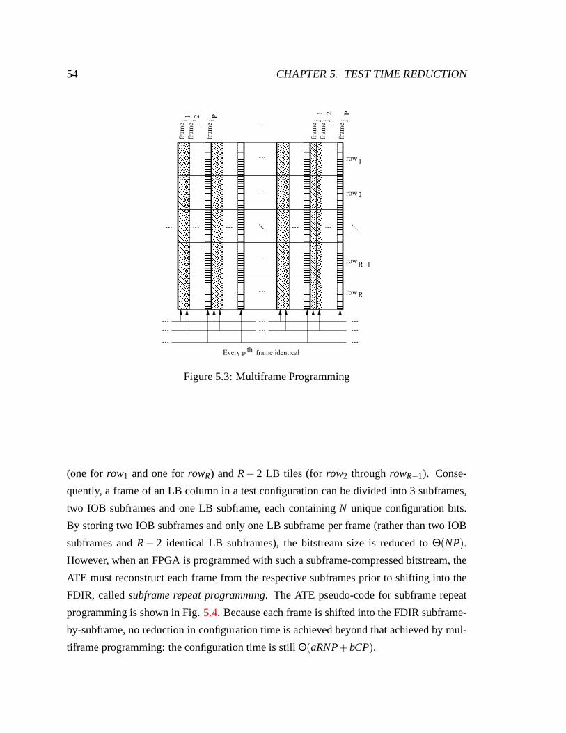
54 CHAPTER 5. TEST TIME REDUCTION
6 66 66 66 66 66 66 66 66 66 66 66 66 66 66 66 66 66 66 66 66 66 66 66 66 66 66 66 66 66 66 66 66 66 66 6
77777777777777777777777777777777777
8 88 88 88 88 88 88 88 88 88 88 88 88 88 88 88 88 88 88 88 88 88 88 88 88 88 88 88 88 88 88 88 88 88 88 8
99999999999999999999999999999999999
: :: :: :: :: :: :: :: :: :: :: :: :: :: :: :: :: :: :
;;;;;;;;;;;;;;;;;;
< << << << << << << << << << << << << << << << << << << << << << << << << << << << << << << << << << << <
===================================
> >> >> >> >> >> >> >> >> >> >> >> >> >> >> >> >> >> >> >> >> >> >> >> >> >> >> >> >> >> >> >> >> >> >> >
???????????????????????????????????
@ @@ @@ @@ @@ @@ @@ @@ @@ @@ @@ @@ @@ @@ @@ @@ @@ @@ @
AAAAAAAAAAAAAAAAAA
BBBBBBBBBBBBBBBBBBBBBBBBBBBBBBBBBBB
CCCCCCCCCCCCCCCCCCCCCCCCCCCCCCCCCCC
D DD DD DD DD DD DD DD DD DD DD DD DD DD DD DD DD DD DD DD DD DD DD DD DD DD DD DD DD DD DD DD DD DD DD D
E EE EE EE EE EE EE EE EE EE EE EE EE EE EE EE EE EE EE EE EE EE EE EE EE EE EE EE EE EE EE EE EE EE EE E
FFFFFFFFFFFFFFFFFF
GGGGGGGGGGGGGGGGGG
HHHHHHHHHHHHHHHHHHHHHHHHHHHHHHHHHHH
IIIIIIIIIIIIIIIIIIIIIIIIIIIIIIIIIII
JJJJJJJJJJJJJJJJJJJJJJJJJJJJJJJJJJJ
KKKKKKKKKKKKKKKKKKKKKKKKKKKKKKKKKKK
LLLLLLLLLLLLLLLLLL
MMMMMMMMMMMMMMMMMM
NNNOOO PPPQQQ
fram
ei 1
fram
ei P
fram
ej
1j
2fr
ame
2ifr
ame
fram
ej
P
rowR−1
rowR
row2
row1
Every p th frame identical
RRRRRSSSSS
TTTTTUUUUU
VVVVVWWWWW
XXXXXXX
YYYYYYY
ZZZZZZZ
[[[[[[[
Figure 5.3: Multiframe Programming
(one for row1 and one forrowR) andR−2 LB tiles (for row2 throughrowR−1). Conse-
quently, a frame of an LB column in a test configuration can be divided into 3 subframes,
two IOB subframes and one LB subframe, each containingN unique configuration bits.
By storing two IOB subframes and only one LB subframe per frame (rather than two IOB
subframes andR− 2 identical LB subframes), the bitstream size is reduced toΘ(NP).
However, when an FPGA is programmed with such a subframe-compressed bitstream, the
ATE must reconstruct each frame from the respective subframes prior to shifting into the
FDIR, calledsubframe repeat programming. The ATE pseudo-code for subframe repeat
programming is shown in Fig.5.4. Because each frame is shifted into the FDIR subframe-
by-subframe, no reduction in configuration time is achievedbeyond that achieved by mul-
tiframe programming: the configuration time is stillΘ(aRNP+bCP).
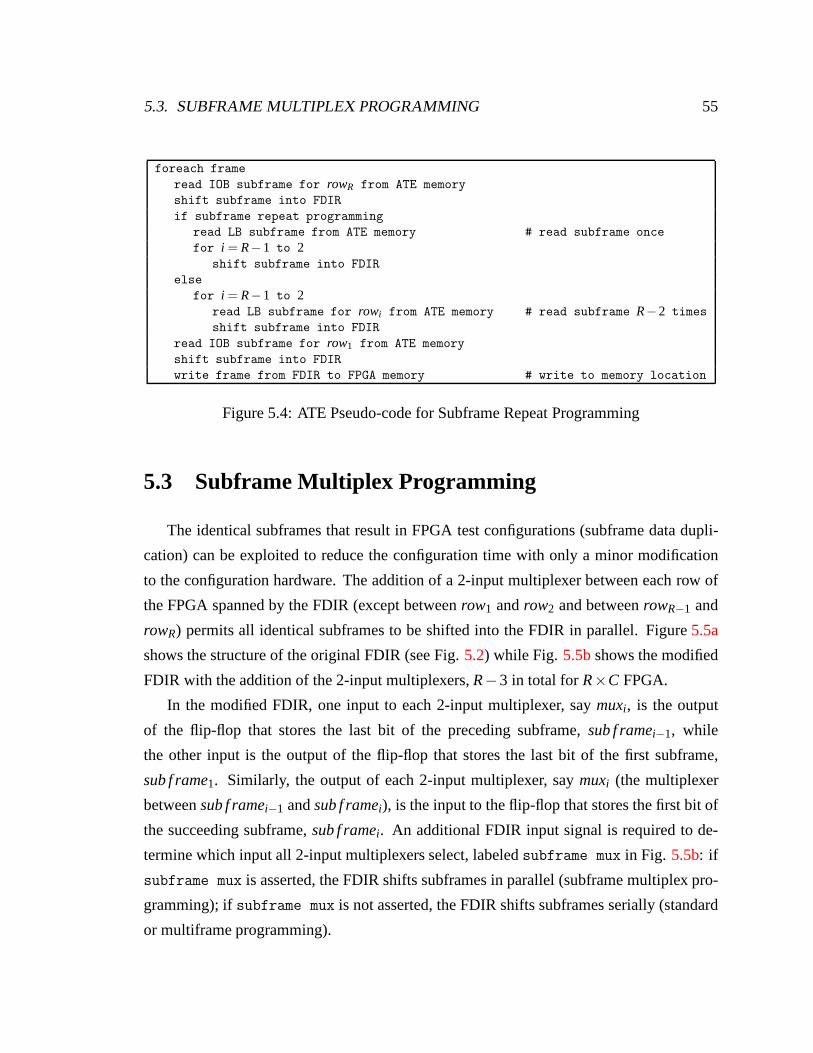
5.3. SUBFRAME MULTIPLEX PROGRAMMING 55
foreach frame
read IOB subframe for rowR from ATE memory
shift subframe into FDIR
if subframe repeat programming
read LB subframe from ATE memory # read subframe once
for i = R−1 to 2shift subframe into FDIR
else
for i = R−1 to 2read LB subframe for rowi from ATE memory # read subframe R−2 times
shift subframe into FDIR
read IOB subframe for row1 from ATE memory
shift subframe into FDIR
write frame from FDIR to FPGA memory # write to memory location
Figure 5.4: ATE Pseudo-code for Subframe Repeat Programming
5.3 Subframe Multiplex Programming
The identical subframes that result in FPGA test configurations (subframe data dupli-
cation) can be exploited to reduce the configuration time with only a minor modification
to the configuration hardware. The addition of a 2-input multiplexer between each row of
the FPGA spanned by the FDIR (except betweenrow1 androw2 and betweenrowR−1 and
rowR) permits all identical subframes to be shifted into the FDIRin parallel. Figure5.5a
shows the structure of the original FDIR (see Fig.5.2) while Fig. 5.5bshows the modified
FDIR with the addition of the 2-input multiplexers,R−3 in total forR×C FPGA.
In the modified FDIR, one input to each 2-input multiplexer, say muxi , is the output
of the flip-flop that stores the last bit of the preceding subframe, sub f ramei−1, while
the other input is the output of the flip-flop that stores the last bit of the first subframe,
sub f rame1. Similarly, the output of each 2-input multiplexer, saymuxi (the multiplexer
betweensub f ramei−1 andsub f ramei), is the input to the flip-flop that stores the first bit of
the succeeding subframe,sub f ramei. An additional FDIR input signal is required to de-
termine which input all 2-input multiplexers select, labeledsubframe mux in Fig. 5.5b: if
subframe mux is asserted, the FDIR shifts subframes in parallel (subframe multiplex pro-
gramming); ifsubframe mux is not asserted, the FDIR shifts subframes serially (standard
or multiframe programming).
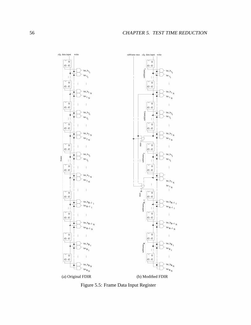
56 CHAPTER 5. TEST TIME REDUCTION
11bit_b
11bit
N1bit_b
1bitN
21bit_b
21bit
2bit_bN
2bitN
31bit
31bit_b
3bit_bN
3bitN
R−1bit_b1
R−1bit1
NR−1bit_b
bit R−1 N
Rbit_b1
Rbit1
bit_bR N
RbitN
DQQ
DQQ
DQQ
DQQ
DQQ
DQQ
DQQ
DQQ
DQQ
DQQ
writecfg. data input
fram
e
(a) Original FDIR
DQQ
DQQ
DQQ
DQQ
DQQ
DQQ
DQQ
DQQ
DQQ
DQQ
subfr
am
e1
subfr
am
e2
subfr
am
e3
subfr
am
eR
−1
subfr
am
eR
mux
R−
1m
ux
3
bit_bR N
RbitN
11bit_b
11bit
N1bit_b
1bitN
21bit_b
21bit
2bit_bN
2bitN
31bit
31bit_b
3bitN
3bit_bN
R−1bit1
R−1bit_b1
NR−1bit_b
bit R−1 N
Rbit_b1
Rbit1
cfg. data input writesubframe mux
(b) Modified FDIR
Figure 5.5: Frame Data Input Register
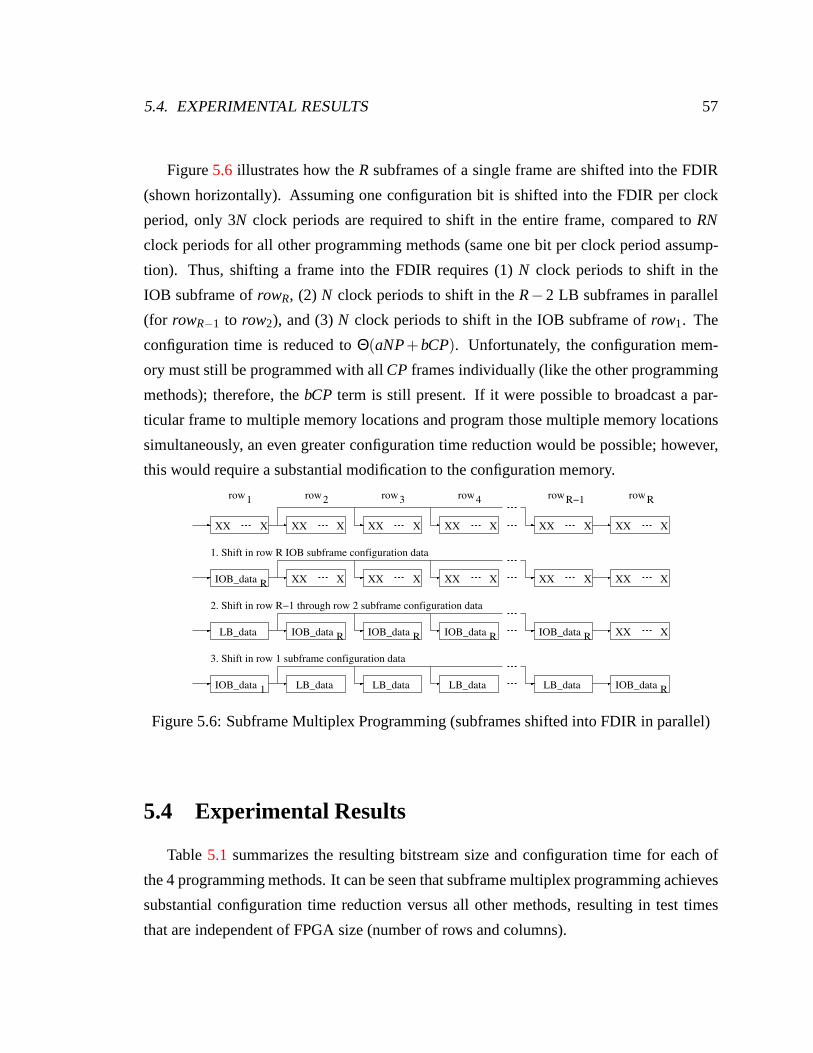
5.4. EXPERIMENTAL RESULTS 57
Figure5.6 illustrates how theR subframes of a single frame are shifted into the FDIR
(shown horizontally). Assuming one configuration bit is shifted into the FDIR per clock
period, only 3N clock periods are required to shift in the entire frame, compared toRN
clock periods for all other programming methods (same one bit per clock period assump-
tion). Thus, shifting a frame into the FDIR requires (1)N clock periods to shift in the
IOB subframe ofrowR, (2) N clock periods to shift in theR−2 LB subframes in parallel
(for rowR−1 to row2), and (3)N clock periods to shift in the IOB subframe ofrow1. The
configuration time is reduced toΘ(aNP+bCP). Unfortunately, the configuration mem-
ory must still be programmed with allCP frames individually (like the other programming
methods); therefore, thebCP term is still present. If it were possible to broadcast a par-
ticular frame to multiple memory locations and program those multiple memory locations
simultaneously, an even greater configuration time reduction would be possible; however,
this would require a substantial modification to the configuration memory.
XX X XX X XX X XX X XX X XX X
XX X XX X XX X XX X XX X
XX X
IOB_data R
IOB_data R IOB_data R IOB_data R IOB_data R
IOB_data RIOB_data 1
LB_data
LB_data LB_data LB_data LB_data
row1 row2 row3 4row rowR−1 Rrow
1. Shift in row R IOB subframe configuration data
3. Shift in row 1 subframe configuration data
2. Shift in row R−1 through row 2 subframe configuration data
Figure 5.6: Subframe Multiplex Programming (subframes shifted into FDIR in parallel)
5.4 Experimental Results
Table5.1 summarizes the resulting bitstream size and configuration time for each of
the 4 programming methods. It can be seen that subframe multiplex programming achieves
substantial configuration time reduction versus all other methods, resulting in test times
that are independent of FPGA size (number of rows and columns).
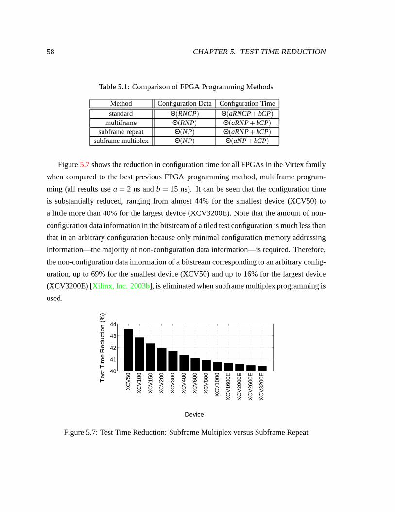
58 CHAPTER 5. TEST TIME REDUCTION
Table 5.1: Comparison of FPGA Programming Methods
Method Configuration Data Configuration Time
standard Θ(RNCP) Θ(aRNCP+bCP)
multiframe Θ(RNP) Θ(aRNP+bCP)
subframe repeat Θ(NP) Θ(aRNP+bCP)
subframe multiplex Θ(NP) Θ(aNP+bCP)
Figure5.7shows the reduction in configuration time for all FPGAs in theVirtex family
when compared to the best previous FPGA programming method,multiframe program-
ming (all results usea = 2 ns andb = 15 ns). It can be seen that the configuration time
is substantially reduced, ranging from almost 44% for the smallest device (XCV50) to
a little more than 40% for the largest device (XCV3200E). Note that the amount of non-
configuration data information in the bitstream of a tiled test configuration is much less than
that in an arbitrary configuration because only minimal configuration memory addressing
information—the majority of non-configuration data information—is required. Therefore,
the non-configuration data information of a bitstream corresponding to an arbitrary config-
uration, up to 69% for the smallest device (XCV50) and up to 16% for the largest device
(XCV3200E) [Xilinx, Inc. 2003b], is eliminated when subframe multiplex programming is
used.
40
41
42
43
44
Device
XC
V50
XC
V10
0
XC
V15
0
XC
V20
0
XC
V30
0
XC
V40
0
XC
V60
0
XC
V80
0
XC
V10
00
XC
V16
00E
XC
V20
00E
XC
V26
00E
XC
V32
00E
Tes
t Tim
e R
educ
tion
(%)
Figure 5.7: Test Time Reduction: Subframe Multiplex versusSubframe Repeat
5.5. SUMMARY 59
5.5 Summary
Adequate fault coverage of an FPGA is achieved by programming and testing the de-
vice with many test configurations. Because the configuration time far exceeds the test
vector application and output response observation time per test configuration, total test
time is dominated by configuration time, especially for large FPGAs. By adding several
2-input multiplexers to the FDIR of an FPGA (R−3 multiplexers for anR×C FPGA), the
configuration time can be (1) greatly reduced, and (2) made nearly constant with respect
to FPGA size. It is shown for the Virtex FPGAs that a configuration time reduction of
between 40% (largest FPGA) and 44% (smallest FPGA) is achieved compared to the best
previous programming method (subframe repeat programming).

60 CHAPTER 5. TEST TIME REDUCTION
This page intentionally left blank.

Part III
Diagnosis
61
Chapter 6
Bridge Fault Location
6.1 Motivation and Previous Work
Fault location is an important part of fault diagnosis sinceit is usually necessary to
locate a fault to identify the underlying defect. Because ofthe abundant logic and routing
resources in an FPGA (most of which remain unused during normal operation), a manufac-
turing defect can be tolerated by (1) locating the resultingfault, and (2) avoiding the fault
when mapping a logic design to the device. Note thatdefect tolerancedescribes the fault
location and fault avoidance process implemented by the manufacturer prior to device op-
eration whilefault tolerancedescribes the process implemented by the device during oper-
ation (for example concurrent error detection). Defect tolerant FPGAs that can implement
only certain logic functions are calledapplication-dependentFPGAs [Xilinx, Inc. 2003c].
Detecting bridge faults is important since they model the majority of defects
[Fantini and Morandi 1985] [Ferguson and Larrabee 1991]. Furthermore, because the
majority of an FPGA is its interconnection network and due tothe high density of the
physical layout in deep sub-micron process technologies, interconnect bridge faults are an
important concern in FPGAs.
There are many Boolean techniques that can locate a stuck-atfault in an FPGA
[Wang and Huang 1998] [Yu et al. 1998] [Wang and Tsai 1999] [Abramovici et al. 1999]
[Das and Touba 1999] [Yu et al. 1999] [Abramovici and Stroud 2000]
[Harris and Tessier 2000a] [Stroud et al. 2001] [Abramovici and Stroud 2001]
[Lu and Chen 2002] [Stroud et al. 2002] [Harris and Tessier 2002]. However, as
discussed in Chap.4, interconnect bridge faults are an important concern in FPGAs, but
62
6.2. DIFFERENTIALIDDQ FAULT LOCATION 63
may not be detected, and therefore unable to be located, using Boolean tests. Specifically,
some shorts caused by stuck-on transistors in transmission-gate multiplexers, equivalent
to a stuck-on PIP in a switch matrix multiplexer, can only be detected viaIDDQ test
[Makar and McCluskey 1996]. A stuck-on PIP creates a bridge fault since it shorts signal
lines, for example interconnects.
6.2 Differential IDDQ Fault Location
6.2.1 Overview
The differentialIDDQ test discussed in Chap.4, which detects interconnect bridge faults,
can also be used to locate the fault. The location process consists of several iterations of:
(1) divide the set of nets in a test configuration into partitions, (2) test the FPGA with each
partition independently via differentialIDDQ, and (3) eliminate the nets contained in the
fault-free partitions from the set of nets to be considered in the next iteration (anet is the
concatenation of several interconnects, or wire segments,that forms a path between logic
blocks or input/output blocks). The number of iterations islogarithmic in the number of
nets in the test configuration; therefore, the technique scales with FPGA size and can be
used for very large devices. Furthermore, because only device configurations and current
measurements are required, the fault location process is easily automated.
The setS is defined as the set of nets, or used interconnects, in a test configuration—
either a failing differentialIDDQ test configuration (for an application-independent FPGA)
or a failing logic design (for an application-dependent FPGA). These test configurations
are designed to detect bridge faults between the interconnects driven to logic-0, used inter-
connects, and those driven to logic-1, unused interconnects (see Chap.4). Therefore, if an
FPGA is programmed with such a test configuration and fails differentialIDDQ test, it must
contain a bridge between some interconnect inS(used interconnect) and some interconnect
not in S (unused interconnect). Thus, every net inS is said to be potentially faulty (poten-
tially bridged to an interconnect not inS). The fault location process iteratively identifies
and eliminates fault-free nets fromSuntil only a single net, the faulty net, remains. Since
all nets ofSare driven to logic-0 in each test configuration and all unused interconnects are
64 CHAPTER 6. BRIDGE FAULT LOCATION
driven to logic-1 by default (pulled up by the level-restorecircuitry on the output of each
switch matrix multiplexer), a net is eliminated fromSsimply by reprogramming the driving
logic element to drive a logic-1: a look-up table is reprogrammed to implementF = 1 and
a bistable is reprogrammed with the initial conditioninit = 1.
Note that a faulty net, not an individual faulty interconnect, is identified by the location
process since all interconnects of a net are driven to the same logic value by the driving
logic element. To identify the faulty interconnect, a differentialIDDQ version of the remove-
and-reroute technique [Tahoori 2002a] can be applied to the faulty net, which will not be
discussed further. Additionally, the net identified to be faulty is only one of the bridged
nets of the bridge fault. To locate the other bridged net (or nets), the fault location process
is simply applied a second time to the FPGA using a test configuration that is the inverse
of the original, discussed in Sec.6.2.2.
6.2.2 Fault Search
During each iteration of the fault location process, the nets of the fault-free partitions
(partitions that do not display an elevated signature current) are eliminated from the setS.
Consequently, two criteria must be met during each iteration of the fault search. First, to
ensure the iterative process converges to locate a bridged net, no net inScan be included
in all partitions. Second, without knowing the expected magnitude of the signature current
for each partition (interconnect leakage current plus a possible fault current, see Table4.1
in Chap.4), the partitions ofSmust be balanced such that the interconnect leakage current
for each partition is approximately equal. To first order this balancing is accomplished
simply by equalizing the number of nets in each partition; more precise balancing can be
accomplished by explicitly equalizing the number of PIPs, although experimental results
show this is unnecessary.
For simplicity and without loss of generality, assume that during each iteration the setS
is always divided into two partitions,P1 andP2 (binary search), and a single bridge fault is
to be located. If the partitioning criteria stated in the previous paragraph are met (balanced
partitions with no net included in all partitions), then only the faulty partition—the one
containing the faulty net—will have an elevated signature current, which is larger than the
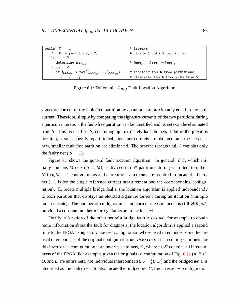
6.2. DIFFERENTIALIDDQ FAULT LOCATION 65
while |S| > 1 # iterate
P1 . . .PN = partition(S,N) # divide S into N partitions
foreach Pi
determine IDDQsigi# IDDQsigi
= IDDQtoti− IDDQre f
foreach Pi
if IDDQsigi< max(IDDQsig1
, . . . , IDDQsigN) # identify fault-free partitions
S = S - Pi # eliminate fault-free nets from S
Figure 6.1: DifferentialIDDQ Fault Location Algorithm
signature current of the fault-free partition by an amount approximately equal to the fault
current. Therefore, simply by comparing the signature currents of the two partitions during
a particular iteration, the fault-free partition can be identified and its nets can be eliminated
from S. This reduced setS, containing approximately half the nets it did in the previous
iteration, is subsequently repartitioned, signature currents are obtained, and the nets of a
new, smaller fault-free partition are eliminated. The process repeats untilScontains only
the faulty net (|S| = 1).
Figure6.1 shows the general fault location algorithm. In general, ifS, which ini-
tially containsM nets (|S| = M), is divided intoN partitions during each iteration, then
NdlogNMe+ 1 configurations and current measurements are required to locate the faulty
net (+1 is for the single reference current measurement and the corresponding configu-
ration). To locate multiple bridge faults, the location algorithm is applied independently
to each partition that displays an elevated signature current during an iteration (multiple
fault currents). The number of configurations and current measurements is stillΘ(logM)
provided a constant number of bridge faults are to be located.
Finally, if location of the other net of a bridge fault is desired, for example to obtain
more information about the fault for diagnosis, the location algorithm is applied a second
time to the FPGA using aninversetest configuration whose used interconnects are the un-
used interconnects of the original configuration andvice versa. The resulting set of nets for
this inverse test configuration is an inverse set of nets,S′, whereS∪S′ contains all intercon-
nects of the FPGA. For example, given the original test configuration of Fig.6.2a(A, B, C,
D, andE are entire nets, not individual interconnects),S= B,D and the bridged netB is
identified as the faulty net. To also locate the bridged netC, the inverse test configuration
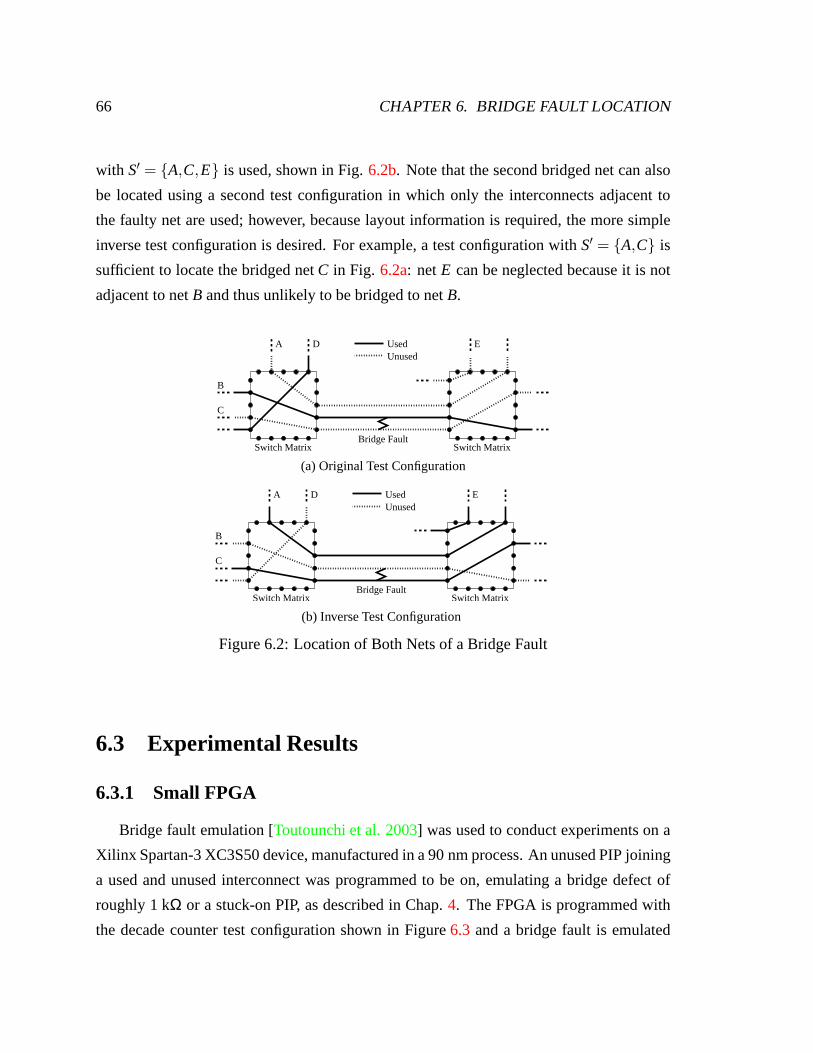
66 CHAPTER 6. BRIDGE FAULT LOCATION
with S′ = A,C,E is used, shown in Fig.6.2b. Note that the second bridged net can also
be located using a second test configuration in which only theinterconnects adjacent to
the faulty net are used; however, because layout information is required, the more simple
inverse test configuration is desired. For example, a test configuration withS′ = A,C is
sufficient to locate the bridged netC in Fig. 6.2a: netE can be neglected because it is not
adjacent to netB and thus unlikely to be bridged to netB.
UsedUnused
Switch Matrix Switch Matrix
A
B
C
Bridge Fault
D E
(a) Original Test Configuration
UsedUnused
Switch Matrix Switch Matrix
A
B
C
Bridge Fault
D E
(b) Inverse Test Configuration
Figure 6.2: Location of Both Nets of a Bridge Fault
6.3 Experimental Results
6.3.1 Small FPGA
Bridge fault emulation [Toutounchi et al. 2003] was used to conduct experiments on a
Xilinx Spartan-3 XC3S50 device, manufactured in a 90 nm process. An unused PIP joining
a used and unused interconnect was programmed to be on, emulating a bridge defect of
roughly 1 kΩ or a stuck-on PIP, as described in Chap.4. The FPGA is programmed with
the decade counter test configuration shown in Figure6.3 and a bridge fault is emulated
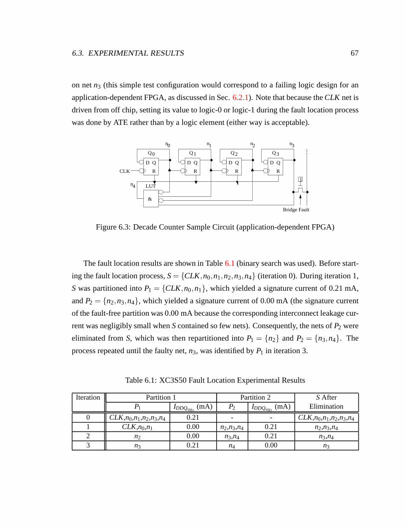
6.3. EXPERIMENTAL RESULTS 67
on netn3 (this simple test configuration would correspond to a failing logic design for an
application-dependent FPGA, as discussed in Sec.6.2.1). Note that because theCLK net is
driven from off chip, setting its value to logic-0 or logic-1during the fault location process
was done by ATE rather than by a logic element (either way is acceptable).
R
QD
R
QD
R
QD
R
QD
Q2 Q3
n3n1n0 2n
4n
&
Q1Q0
1
CLK
LUT
Bridge Fault
Figure 6.3: Decade Counter Sample Circuit (application-dependent FPGA)
The fault location results are shown in Table6.1(binary search was used). Before start-
ing the fault location process,S= CLK,n0,n1,n2,n3,n4 (iteration 0). During iteration 1,
Swas partitioned intoP1 = CLK,n0,n1, which yielded a signature current of 0.21 mA,
andP2 = n2,n3,n4, which yielded a signature current of 0.00 mA (the signaturecurrent
of the fault-free partition was 0.00 mA because the corresponding interconnect leakage cur-
rent was negligibly small whenScontained so few nets). Consequently, the nets ofP2 were
eliminated fromS, which was then repartitioned intoP1 = n2 andP2 = n3,n4. The
process repeated until the faulty net,n3, was identified byP1 in iteration 3.
Table 6.1: XC3S50 Fault Location Experimental Results
Iteration Partition 1 Partition 2 SAfterP1 IDDQsig1
(mA) P2 IDDQsig2(mA) Elimination
0 CLK,n0,n1,n2,n3,n4 0.21 - - CLK,n0,n1,n2,n3,n4
1 CLK,n0,n1 0.00 n2,n3,n4 0.21 n2,n3,n4
2 n2 0.00 n3,n4 0.21 n3,n4
3 n3 0.21 n4 0.00 n3
68 CHAPTER 6. BRIDGE FAULT LOCATION
6.3.2 Large FPGA
A similar experiment was conducted on a much larger FPGA, a Spartan-3 XC3S1000
(also manufactured in a 90 nm process). An emulated bridge fault between different pairs
of used interconnects (logic-0) and unused interconnects (logic-1) throughout the FPGA
was injected into a manufacturing test configuration and then located with a binary search
using the fault location process. The total number of nets inthe manufacturing test con-
figuration, consisting of several ILAs which together use all logic blocks of the FPGA,
is 30720 nets (M = 30720). Onlydlog230720e = 15 iterations and 2dlog230720e+1 = 31
configurations and current measurements were required to locate the faulty net in each case.
Figure6.4a shows the signature currents for both partitions during each iteration,
plotted such thatP1 is always fault-free. Figure6.4b shows the estimated fault current,
IDDQsig2− IDDQsig1
, during each iteration. Thex-axis in both plots is labeled by the number
of nets in each partition during each iteration. It can be seen that the signature current of
the fault-free partition converges to zero while the signature current of the faulty partition
converges to the fault current (determined to be 0.61 mA in the last iteration of Fig.6.4b).
Balancing the signature currents by equalizing the number of nets in each partition resulted
in a maximum fault current estimation error (difference between the estimated fault current
and the actual fault current) of only 3%.
6.4 Summary
Fault location is an important part of fault diagnosis. A bridge fault in an FPGA, which
may not be detectable using Boolean tests (and therefore unable to be located), may be
located by employing differentialIDDQ test. The location process consists of several it-
erations of: (1) divide the set of nets in a test configurationinto partitions, (2) test the
FPGA with each partition independently via differentialIDDQ, and (3) eliminate the nets
contained in the fault-free partitions from the set of nets to be considered in the next itera-
tion. Because the number of iterations is logarithmic in thenumber of nets, the technique
scales with FPGA size and can be used for very large devices. Also, because only device
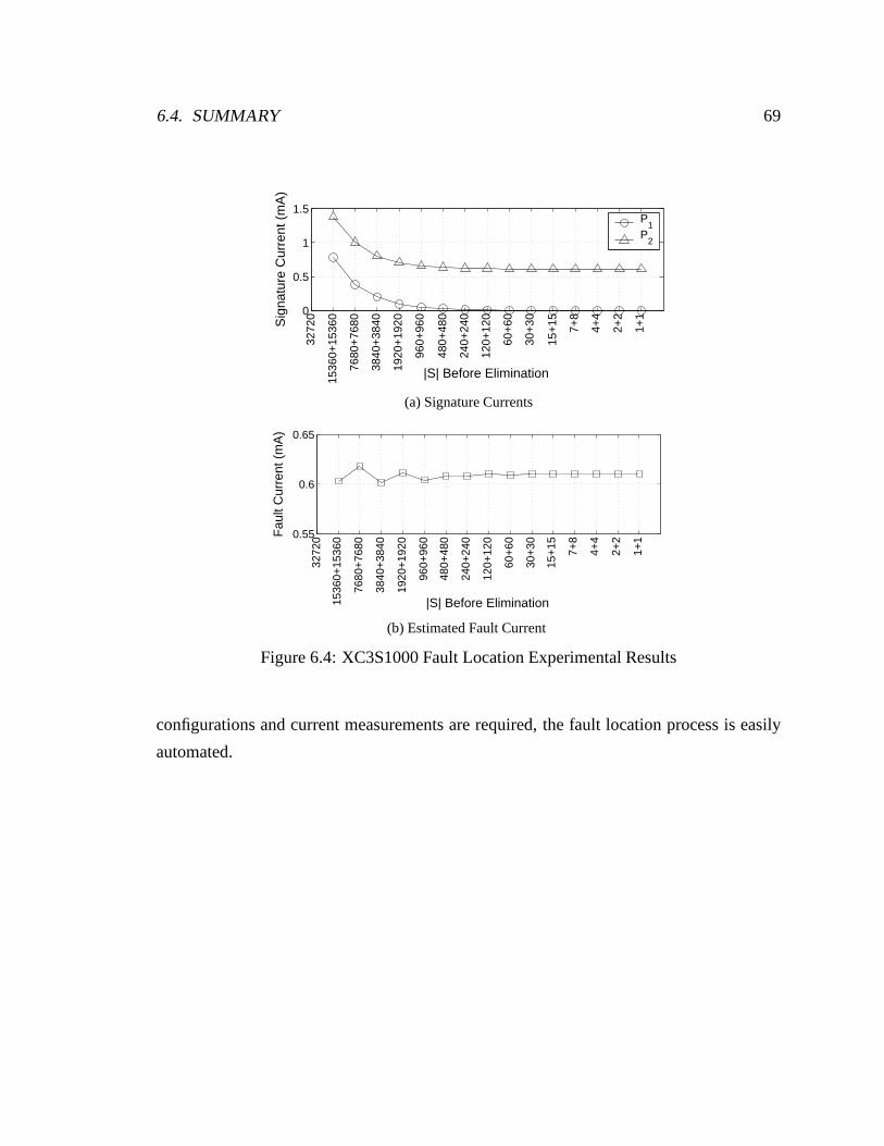
6.4. SUMMARY 69
0
0.5
1
1.5
|S| Before Elimination
Sig
natu
re C
urre
nt (
mA
)
3272
0
1536
0+15
360
7680
+76
80
3840
+38
40
1920
+19
20
960+
960
480+
480
240+
240
120+
120
60+
60
30+
30
15+
15
7+8
4+4
2+2
1+1
P1
P2
(a) Signature Currents
0.55
0.6
0.65
|S| Before Elimination
Fau
lt C
urre
nt (
mA
)
3272
0
1536
0+15
360
7680
+76
80
3840
+38
40
1920
+19
20
960+
960
480+
480
240+
240
120+
120
60+
60
30+
30
15+
15 7+8
4+4
2+2
1+1
(b) Estimated Fault Current
Figure 6.4: XC3S1000 Fault Location Experimental Results
configurations and current measurements are required, the fault location process is easily
automated.

70 CHAPTER 6. BRIDGE FAULT LOCATION
This page intentionally left blank.
Chapter 7
Automated Fault Diagnosis
7.1 Motivation and Previous Work
Fault diagnosis is the process of determining the cause of a device failure, important
because the information obtained can be used to make manufacturing improvements to in-
crease yield. A common method is stuck-at fault diagnosis, which (1) uses stuck-at faults
to model the behavior of a defect, and (2) identifies the smallest possible set offault candi-
dates, or faults that could explain the failure (explain the output response of the defective
device). Although the stuck-at fault model is not an accurate model of real defects, for ex-
ample a bridge, it is appealing to use for diagnosis for several reasons. First, the simplicity
of the stuck-at fault model permits simple mathematical treatment of the faults considered
during diagnosis. Next, the number of stuck-at faults in a circuit is much smaller than
the number of more realistic faults. Finally, the cost of simulating stuck-at faults (done
to match the output response of the simulated circuit with that of the defective device) is
usually much less than simulating realistic faults [Chess et al. 1995].
Any diagnosis technique can be categorized as one of two possible approaches, cause-
effect or effect-cause [Abramovici et al. 1990]. In cause-effectanalysis a fault dictionary is
created by enumerating all possible faults in a circuit (causes) and determining the resulting
circuit responses (effects) via fault simulation for some input stimuli (a set of test vectors).
An attempt is then made to match the response of the defectivecircuit (to an input stimulus)
to one of the responses in the fault dictionary. Ineffect-causeanalysis the response of
the defective circuit to an input stimulus is obtained first and then an attempt is made to
determine which faults could have caused that response.
71
72 CHAPTER 7. AUTOMATED FAULT DIAGNOSIS
Even for a non-configurable circuit, for example an ASIC or microprocessor, the cause-
effect approach is impractical because of the large dictionary size and the correspondingly
long computation time required for dictionary creation (fault simulation). For a config-
urable circuit, an FPGA, the problem is exacerbated becausea fault dictionary must be
created for each of the possibly hundreds of test configurations. Therefore, in practice FP-
GAs are diagnosed using the effect-cause approach; however, it is a manual andad hoc
process taking days to weeks to diagnose a single device. First, an FPGA is tested with a
particular test configuration (and test vectors), usually one for which it failed manufactur-
ing test. Then, multiple trial-and-error steps are conducted, each consisting of: (1) modify
the test configuration or test vectors (or create or use different ones) to reflect the response
seen by the device when tested, and (2) retest the FPGA.
There are many formal FPGA diagnosis techniques that try to reduce the diagnosis
time, all based on generating in advance a set of test configurations and test vectors
(or simply a set of test configurations ifBuilt-in Self Test(BIST) is used) whose
output responses in the presence of a fault can be used to identify the fault. Some
techniques diagnose only faults in the logic resources of anFPGA [Wang and Tsai 1999]
[Abramovici and Stroud 2000] [Abramovici and Stroud 2001] [Lu and Chen 2002] while
others also diagnose faults in the interconnection network[Wang and Huang 1998]
[Yu et al. 1999] [Abramovici et al. 1999] [Harris and Tessier 2000a] [Stroud et al. 2001]
[Stroud et al. 2002] [Harris and Tessier 2002]. However, for all techniques a unique set of
test configurations and test vectors must be generated for each differently sized FPGA of a
particular architecture. Furthermore, the set of test configurations and test vectors must be
regenerated (if possible) for different FPGA architectures.
7.2 Stuck-at Fault Diagnosis
7.2.1 Overview
The main (and most challenging) part of the previous diagnosis techniques is creating
test configurations, which is done because the existing manufacturing test configurations
7.2. STUCK-AT FAULT DIAGNOSIS 73
are not well suited for diagnosis (they typically have very few primary outputs). The num-
ber of primary outputs of a manufacturing test configurationis kept low for two main
reasons: to (1) reduce pin-count requirements of the ATE, and (2) permit each test configu-
ration to be used for differently sized FPGAs that have different packages and pin-outs (in
many test configurations all logic blocks are simply joined to form a single long ILA that
has a single primary output). In contrast, the presented diagnosis technique is not based
on generating a set of test configurations, but instead takesadvantage of the configura-
bility of an FPGA to make use of the already existing manufacturing test configurations
(overcoming the problem of few primary outputs).
There are two primary benefits to using the existing manufacturing test configurations:
the diagnosis process is (1) very fast, and (2) applicable toany FPGA in production re-
gardless of size or architecture (provided manufacturing test configurations exist to test
devices before being sold to customers). First, compared tothead hocdiagnosis done in
practice, the diagnosis time is reduced from days or weeks toonly hours by eliminating
the entire configuration generation process. Second, compared to the diagnosis techniques
that generate test configurations in advance, no additionalconfigurations must be created
to diagnose FPGAs of different size or architecture. A secondary benefit is that any failure
caused by either a fault in the logic or routing resources, observed during manufacturing
test, is guaranteed to be observed during diagnosis since the fault will be activated in the
exact same manner by the same test configuration.
7.2.2 Diagnosis Process
The diagnosis of an FPGA consists of two main procedures: (1)identify fault candi-
dates, and (2) systematically eliminate fault candidates.Table7.1 lists all required steps
in more detail. Fault candidates are identified in steps 1 through 4 and 7 (step 7 appears
later in the process for implementation reasons, discussedin the fan-in cone logic extrac-
tion section) and fault candidates are eliminated in steps 5, 6, 8, and 9. The entire process
(except step 10) is fully automated, producing a small set offault candidates that are each
verified in step 10.
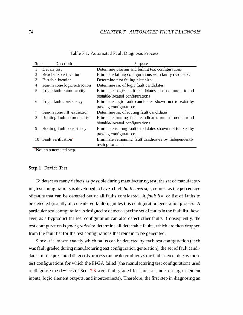
74 CHAPTER 7. AUTOMATED FAULT DIAGNOSIS
Table 7.1: Automated Fault Diagnosis Process
Step Description Purpose1 Device test Determine passing and failing test configurations2 Readback verification Eliminate failing configurations with faulty readbacks3 Bistable location Determine first failing bistables4 Fan-in cone logic extraction Determine set of logic fault candidates5 Logic fault commonality Eliminate logic fault candidatesnot common to all
bistable-located configurations6 Logic fault consistency Eliminate logic fault candidatesshown not to exist by
passing configurations7 Fan-in cone PIP extraction Determine set of routing fault candidates8 Routing fault commonality Eliminate routing fault candidates not common to all
bistable-located configurations9 Routing fault consistency Eliminate routing fault candidates shown not to exist by
passing configurations10 Fault verification∗ Eliminate remaining fault candidates by independently
testing for each∗Not an automated step.
Step 1: Device Test
To detect as many defects as possible during manufacturing test, the set of manufactur-
ing test configurations is developed to have a highfault coverage, defined as the percentage
of faults that can be detected out of all faults considered. Afault list, or list of faults to
be detected (usually all considered faults), guides this configuration generation process. A
particular test configuration is designed to detect a specific set of faults in the fault list; how-
ever, as a byproduct the test configuration can also detect other faults. Consequently, the
test configuration isfault gradedto determine all detectable faults, which are then dropped
from the fault list for the test configurations that remain tobe generated.
Since it is known exactly which faults can be detected by eachtest configuration (each
was fault graded during manufacturing test configuration generation), the set of fault candi-
dates for the presented diagnosis process can be determinedas the faults detectable by those
test configurations for which the FPGA failed (the manufacturing test configurations used
to diagnose the devices of Sec.7.3 were fault graded for stuck-at faults on logic element
inputs, logic element outputs, and interconnects). Therefore, the first step in diagnosing an
7.2. STUCK-AT FAULT DIAGNOSIS 75
FPGA is to test the device with all, or at least many, of these manufacturing test configura-
tions to determine for which the device fails and for which itpasses. This information is not
collected during manufacturing test because an FPGA is rejected immediately after it first
fails (to reduce test time and therefore test cost); to avoidusing expensive ATE during this
diagnosis step, inexpensive ATE can be used, as was done to obtain the experimental re-
sults of Sec.7.3. Note that fault grading is not considered a step in the presented diagnosis
process because it is typically done during manufacturing test configuration generation.
A failing test configurationis one for which an FPGA fails while apassing test config-
uration is one for which an FPGA passes. Although more fault candidates are identified
when the device is tested with more test configurations (there are more failing configura-
tions), the number of fault candidates that can be eliminated also increases (there are more
passing configurations). Therefore, a finerresolution—fewer fault candidates—ultimately
results by maximizing the number of test configurations withwhich the device is tested.
Step 2: Readback Verification
After device test has identified the set of fault candidates (literally millions of candi-
dates), the next step is to systematically reduce this set. The first method is to locate the first
bistable (or bistables) in the FPGA to capture a faulty value—thefirst failing bistable—for
each failing test configuration (different bistables may beidentified for each test configu-
ration because each test configuration either implements a different logic function or is a
different mapping of the same logic function to the FPGA). Bistable location is done using
the special DFT hardware of contemporary FPGAs that enablesreadback [Holfich 1994].
Readbackis the scanning out serially of both configuration data and the state of all bista-
bles in an FPGA (conceptually the inverse of configuration),which permits the state of the
device to be captured at any time. However, because the device being diagnosed is faulty,
readback may not function correctly; readback functionality must therefore be verified.
The result of capturing the device state via readback is areadback file, which contains
both the configuration memory bits and the bistable data bitsof an FPGA. Any bit of a
readback file may be erroneous, or faulty. To continue the diagnosis process, it is necessary
to determine (1) which bits are faulty, and (2) how the faultybit behaves (random or stuck-
at). To identify a readback bit that is stuck at some logic value (stuck-at bit), a readback
76 CHAPTER 7. AUTOMATED FAULT DIAGNOSIS
file is obtained from the faulty device (device being diagnosed) immediately after it is
programmed with a test configuration and compared to the readback file of a known-good
device obtained in the same manner. Because the state of bothdevices should match,
any bits that differ between the faulty and known-good readback files are faulty. If the
logic value of those faulty bits does not change when additional readback files of the faulty
device are obtained (again immediately after configuration), then those faulty bits are stuck-
at bits. Stuck-at 1 bits are identified by programming both devices with a special all-
zero configuration (everything initialized to logic-0) while stuck-at 0 bits are identified
by programming both devices with a special all-ones configuration (everything initialized
to logic-1). Bits whose logic value changes when additionalreadback files of the faulty
device are obtained are random bits (readback is done in the exact same manner each time,
therefore each subsequent readback file should match the previous).
Faulty readback bits do not necessarily mean that the FPGA cannot be diagnosed using
the presented process: most readback bits will not be used toconduct bistable location
anyway (only about 2-3% of readback bits are meaningful in any given configuration).
Only if there is a stuck-at 0 or stuck-at 1 readback bit that corresponds to a bistable used
in a particular failing test configuration (the readback bitrepresents the data stored in that
bistable) is that test configuration discarded as one for which the first failing bistable can
be located. A random readback bit does not cause a test configuration to be discarded since
a method of majority voting can be used during bistable location (discussed in the bistable
location section).
Step 3: Bistable Location
When a fault is activated, a faulty response may be observed on a primary output;
however, fault activation may have occurred many clock periods before the faulty primary
output is observed (this is what makes the manufacturing test configurations difficult to use
for diagnosis). By obtaining readback files at various timesduring the test of an FPGA, the
first bistable (or bistables) to capture a faulty value (the result of fault activation) can be
determined, thereby using the bistable as a test observation point. Because the fault must
lie in the fan-in coneof this first failing bistable, which is defined as all logic and routing
resources on any path traced backwards from the input of thatbistable to the output of
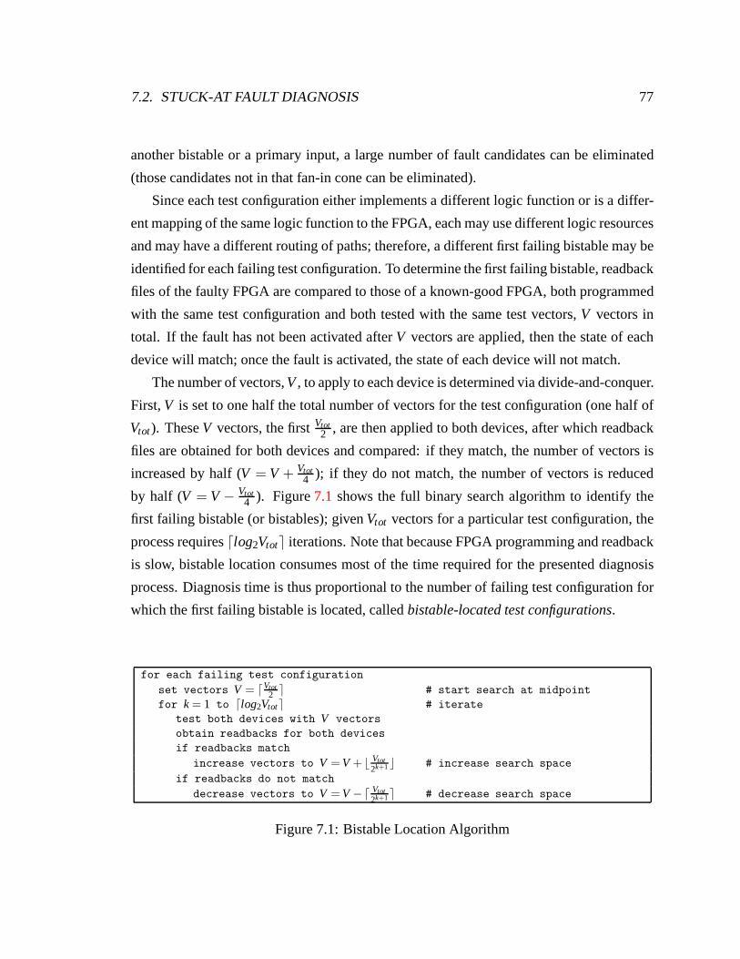
7.2. STUCK-AT FAULT DIAGNOSIS 77
another bistable or a primary input, a large number of fault candidates can be eliminated
(those candidates not in that fan-in cone can be eliminated).
Since each test configuration either implements a differentlogic function or is a differ-
ent mapping of the same logic function to the FPGA, each may use different logic resources
and may have a different routing of paths; therefore, a different first failing bistable may be
identified for each failing test configuration. To determinethe first failing bistable, readback
files of the faulty FPGA are compared to those of a known-good FPGA, both programmed
with the same test configuration and both tested with the sametest vectors,V vectors in
total. If the fault has not been activated afterV vectors are applied, then the state of each
device will match; once the fault is activated, the state of each device will not match.
The number of vectors,V, to apply to each device is determined via divide-and-conquer.
First,V is set to one half the total number of vectors for the test configuration (one half of
Vtot). TheseV vectors, the firstVtot2 , are then applied to both devices, after which readback
files are obtained for both devices and compared: if they match, the number of vectors is
increased by half (V = V + Vtot4 ); if they do not match, the number of vectors is reduced
by half (V = V − Vtot4 ). Figure7.1 shows the full binary search algorithm to identify the
first failing bistable (or bistables); givenVtot vectors for a particular test configuration, the
process requiresdlog2Vtote iterations. Note that because FPGA programming and readback
is slow, bistable location consumes most of the time required for the presented diagnosis
process. Diagnosis time is thus proportional to the number of failing test configuration for
which the first failing bistable is located, calledbistable-located test configurations.
for each failing test configuration
set vectors V = dVtot2 e # start search at midpoint
for k = 1 to dlog2Vtote # iterate
test both devices with V vectors
obtain readbacks for both devices
if readbacks match
increase vectors to V = V + b Vtot2k+1c # increase search space
if readbacks do not match
decrease vectors to V = V −d Vtot2k+1e # decrease search space
Figure 7.1: Bistable Location Algorithm
78 CHAPTER 7. AUTOMATED FAULT DIAGNOSIS
Although a known-good device can be tested ahead of time and the known-good read-
back files can be stored, there is no reason: no delay is incurred by testing the known-good
device in parallel with the faulty device (test both devicesat the same time). Furthermore,
it is impractical to store all possible readback files for theknown-good device because the
required disk space is impractically large. One Readback file is required to store the state of
the known-good device after each additional vector is applied (one readback file forV = 1,
one readback file forV = 2, all the way up to one readback file forV = Vtot), where each
readback file is several megabytes in size. Furthermore,Vtot readbacks are required for
each manufacturing test configuration (Vtot can be different for different configurations, but
is typically several tens of thousands of vectors).
In the location algorithm of Fig.7.1, the faulty device is tested only once withV vec-
tors and only one readback file is obtained per iteration. However, if it was determined by
the readback verification step that random readback bits exist, then the faulty device can
be tested multiple times withV vectors (an odd number of times) and multiple readback
files can be obtained per iteration. The ’correct’ value of each random readback bit during
a particular iteration can be determined by a majority vote between the multiple readback
files and a ’correct’ faulty readback file can be composed for comparison to the known-
good readback file. This majority vote technique was successfully used for both devices
diagnosed in Sec.7.3; it was found that 3 tests (configuration and application ofV vectors)
and readbacks per iteration were sufficient. If a majority vote for random readback bits is
not done then the bistable location algorithm may identify an incorrect first failing bistable:
the random readback bit may result in an incorrect decision (increase or decrease in the
number of vectors,V) during readback comparison. Note that as the number of tests and
readbacks of the faulty device increases, the probability that the bistable location algorithm
will identify an incorrect first failing bistable decreases(unless the logic value of the ran-
dom readback bit has an equal likelihood of being either logic-0 or logic-1). Additionally,
because the faulty device is programmed multiple times and multiple readback files are
obtained (per iteration), the total diagnosis time increases (configuration and readback are
slow).
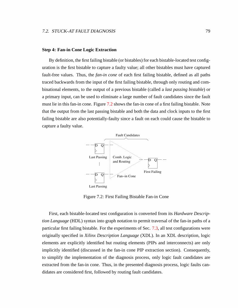
7.2. STUCK-AT FAULT DIAGNOSIS 79
Step 4: Fan-in Cone Logic Extraction
By definition, the first failing bistable (or bistables) for each bistable-located test config-
uration is the first bistable to capture a faulty value; all other bistables must have captured
fault-free values. Thus, thefan-in coneof each first failing bistable, defined as all paths
traced backwards from the input of the first failing bistable, through only routing and com-
binational elements, to the output of a previous bistable (called alast passing bistable) or
a primary input, can be used to eliminate a large number of fault candidates since the fault
must lie in this fan-in cone. Figure7.2shows the fan-in cone of a first failing bistable. Note
that the output from the last passing bistable and both the data and clock inputs to the first
failing bistable are also potentially-faulty since a faulton each could cause the bistable to
capture a faulty value.
D Q
D Q
D Q
Fan−in Cone
and Routing
Fault Candidates
First Failing
Last Passing
Last Passing
Comb. Logic
Figure 7.2: First Failing Bistable Fan-in Cone
First, each bistable-located test configuration is converted from itsHardware Descrip-
tion Language(HDL) syntax into graph notation to permit traversal of the fan-in paths of a
particular first failing bistable. For the experiments of Sec. 7.3, all test configurations were
originally specified inXilinx Description Language(XDL). In an XDL description, logic
elements are explicitly identified but routing elements (PIPs and interconnects) are only
implicitly identified (discussed in the fan-in cone PIP extraction section). Consequently,
to simplify the implementation of the diagnosis process, only logic fault candidates are
extracted from the fan-in cone. Thus, in the presented diagnosis process, logic faults can-
didates are considered first, followed by routing fault candidates.
80 CHAPTER 7. AUTOMATED FAULT DIAGNOSIS
In the graph notation for a given test configuration, each vertex is an input or output of
a logic element and each edge is a net. To determine the set of logic fault candidates, each
fan-in path of the first failing bistable is traversed backwards to the last passing bistable (or
primary input), recording each vertex along the way.
Step 5: Logic Fault Commonality
Up to this point each test configuration has been considered individually, each used to
individually test the FPGA, identifying a set of logic faultcandidates for that particular
test configuration. If only a single fault is assumed to exist(one fault in the FPGA being
diagnosed), then there must be a logic fault candidate that is common to every failing test
configuration (the single fault must be the cause of failure for each test configuration).
Thus, logic fault candidates not common to all bistable-located test configurations can be
eliminated. The number of logic fault candidates that can beeliminated is proportional to
the number of bistable-located test configurations. For both devices diagnosed in Sec.7.3,
it was found that fault-locating only 2–3% of the failing test configurations resulted in
enough fault candidate elimination for successful diagnosis.
The aggregate set of logic fault candidates is the union of all logic fault candidates
identified by each bistable-located test configuration. If elimination yields a very small
aggregate set of logic fault candidates, say no more than 10 (10 is chosen because it is
considered a sufficiently small number of fault candidates to be easily verified by the fault
verification step), then routing fault candidates need not be considered (routing faults steps
should be conducted if routing faults are still suspected).If elimination yields an empty
aggregate set of logic fault candidates, then (1) there are multiple logic faults, (2) there is
one or more routing faults, (3) there are both logic and routing faults, or (4) there is a defect
in the faulty device that is not modeled by a single stuck-at fault (unmodeled defect). To not
eliminate possible logic faults (if multiple faults or an unmodeled defect exists), the empty
aggregate set of logic fault candidates is restored to contain all logic fault candidates and
the diagnosis process is continued.
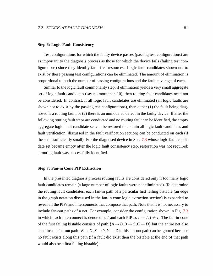
7.2. STUCK-AT FAULT DIAGNOSIS 81
Step 6: Logic Fault Consistency
Test configurations for which the faulty device passes (passing test configurations) are
as important to the diagnosis process as those for which the device fails (failing test con-
figurations) since they identify fault-free resources. Logic fault candidates shown not to
exist by these passing test configurations can be eliminated. The amount of elimination is
proportional to both the number of passing configurations and the fault coverage of each.
Similar to the logic fault commonality step, if eliminationyields a very small aggregate
set of logic fault candidates (say no more than 10), then routing fault candidates need not
be considered. In contrast, if all logic fault candidates are eliminated (all logic faults are
shown not to exist by the passing test configurations), then either (1) the fault being diag-
nosed is a routing fault, or (2) there is an unmodeled defect in the faulty device. If after the
following routing fault steps are conducted and no routing fault can be identified, the empty
aggregate logic fault candidate set can be restored to contain all logic fault candidates and
fault verification (discussed in the fault verification section) can be conducted on each (if
the set is sufficiently small). For the diagnosed device in Sec. 7.3whose logic fault candi-
date set became empty after the logic fault consistency step, restoration was not required:
a routing fault was successfully identified.
Step 7: Fan-in Cone PIP Extraction
In the presented diagnosis process routing faults are considered only if too many logic
fault candidates remain (a large number of logic faults werenot eliminated). To determine
the routing fault candidates, each fan-in path of a particular first failing bistable (an edge
in the graph notation discussed in the fan-in cone logic extraction section) is expanded to
reveal all the PIPs and interconnects that compose that path. Note that it is not necessary to
include fan-out paths of a net. For example, consider the configuration shown in Fig.7.3
in which each interconnect is denoted asI and each PIP asI → J, I 6= J. The fan-in cone
of the first failing bistable consists of pathA→ B,B→C,C→ D but the entire net also
contains the fan-out pathB→ X,X →Y,Y → Z: this fan-out path can be ignored because
no fault exists along this path (if a fault did exist then the bistable at the end of that path
would also be a first failing bistable).
82 CHAPTER 7. AUTOMATED FAULT DIAGNOSIS
D Q
D Q
D Q
B
C
B X
C DA
B X
Y
YZ
B
C
X
Z
DA
Y
Fault−free
Potentially Faulty
Passing Failing
Passing
Figure 7.3: Routing Net (path with fan-out)
Because the XDL specification of a test configuration describes a net by the set of PIPs
it contains and only implicitly identifies the interconnects (PIPI → J implicitly identifies
interconnectsI andJ), it is sufficient to extract only the PIPs in the fan-in cone of each
first failing bistable. Thus, to determine the set of routingfault candidates, each fan-in path
of the first failing bistable is traversed backwards to the last passing bistable (or primary
input), recording each PIP along the way. Note that the routing fault candidates correspond
to stuck-at faults on the input and output of each PIP (each input or output of a PIP is an
interconnect, logic element input, or logic element output).
Step 8: Routing Fault Commonality
Elimination of routing fault candidates via routing fault commonality is analogous to
elimination of logic fault candidates via logic fault commonality. Again, if only a single
fault is assumed to exist (one fault in the FPGA being diagnosed), then there must be some
routing fault candidates that are common to every failing test configuration. Thus, routing
fault candidates not common to all bistable-located test configurations can be eliminated.
The number of routing fault candidates that can be eliminated is proportional to the number
of bistable-located test configurations.
The aggregate set of routing fault candidates is the union ofall routing fault candidates
identified by each bistable-located test configuration. If elimination yields a very small
aggregate set of routing fault candidates (say no more than 10), then diagnosis can imme-
diately conclude with the fault verification step. If elimination yields an empty aggregate
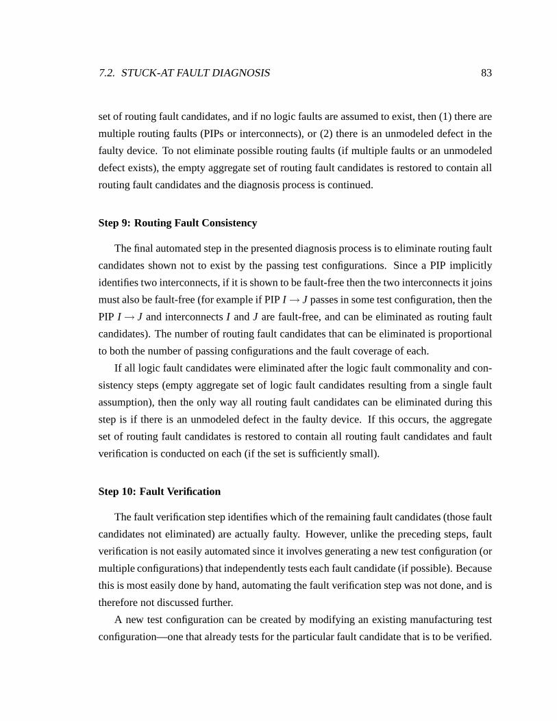
7.2. STUCK-AT FAULT DIAGNOSIS 83
set of routing fault candidates, and if no logic faults are assumed to exist, then (1) there are
multiple routing faults (PIPs or interconnects), or (2) there is an unmodeled defect in the
faulty device. To not eliminate possible routing faults (ifmultiple faults or an unmodeled
defect exists), the empty aggregate set of routing fault candidates is restored to contain all
routing fault candidates and the diagnosis process is continued.
Step 9: Routing Fault Consistency
The final automated step in the presented diagnosis process is to eliminate routing fault
candidates shown not to exist by the passing test configurations. Since a PIP implicitly
identifies two interconnects, if it is shown to be fault-freethen the two interconnects it joins
must also be fault-free (for example if PIPI → J passes in some test configuration, then the
PIP I → J and interconnectsI andJ are fault-free, and can be eliminated as routing fault
candidates). The number of routing fault candidates that can be eliminated is proportional
to both the number of passing configurations and the fault coverage of each.
If all logic fault candidates were eliminated after the logic fault commonality and con-
sistency steps (empty aggregate set of logic fault candidates resulting from a single fault
assumption), then the only way all routing fault candidatescan be eliminated during this
step is if there is an unmodeled defect in the faulty device. If this occurs, the aggregate
set of routing fault candidates is restored to contain all routing fault candidates and fault
verification is conducted on each (if the set is sufficiently small).
Step 10: Fault Verification
The fault verification step identifies which of the remainingfault candidates (those fault
candidates not eliminated) are actually faulty. However, unlike the preceding steps, fault
verification is not easily automated since it involves generating a new test configuration (or
multiple configurations) that independently tests each fault candidate (if possible). Because
this is most easily done by hand, automating the fault verification step was not done, and is
therefore not discussed further.
A new test configuration can be created by modifying an existing manufacturing test
configuration—one that already tests for the particular fault candidate that is to be verified.
84 CHAPTER 7. AUTOMATED FAULT DIAGNOSIS
The manufacturing test configuration is modified to contain only the resource identified by
the fault candidate (for example a PIP or a look-up table) anda minimal amount of re-
sources that permit control and observation of the logic value at the fault candidate location
(for example PIPs and interconnects shown to be fault-free by passing test configurations).
Control can be achieved by creating a path from a primary input to the fault candidate loca-
tion while observation can be achieved by creating a path from the fault candidate location
to a primary output. Note that control and observation can also be achieved by creating a
path from some bistable to the fault candidate location, creating a path from the fault can-
didate location to another bistable, and using readback to control and observe the bistable
inputs and outputs, respectively.
Verifying a fault candidate is done by independently testing for that fault—controlling
and observing the logic value at the fault location while notactivating any of the other fault
candidates. Thus, when a fault candidate is tested (one at a time, each with its own test
configuration) and a failure is observed, and assuming all other elements used to create the
control and observation paths are fault-free, then the failure can only be the result of that
fault candidate and not of any others (or the result of an unmodeled defect). Therefore, a
fault candidate verified in this manner is said to be an actualfault (no longer a candidate).
Although logic fault verification is simply done by independently testing for each logic
fault candidate, routing fault verification requires a little more care since both PIPs and
interconnects must be considered. For example, let the aggregate set of routing fault can-
didates of an FPGA with a single routing fault be PIPsB→C, C→ D, andW →C, iden-
tified via bistable location of the two manufacturing test configurations shown in Fig.7.4
(potentially-faulty PIPs are bold). Clearly the common PIPC→ D may be faulty; however,
either interconnectC or D may instead be faulty. Thus, new test configurations used for
routing fault candidate verification must test for PIPs and interconnects independently.
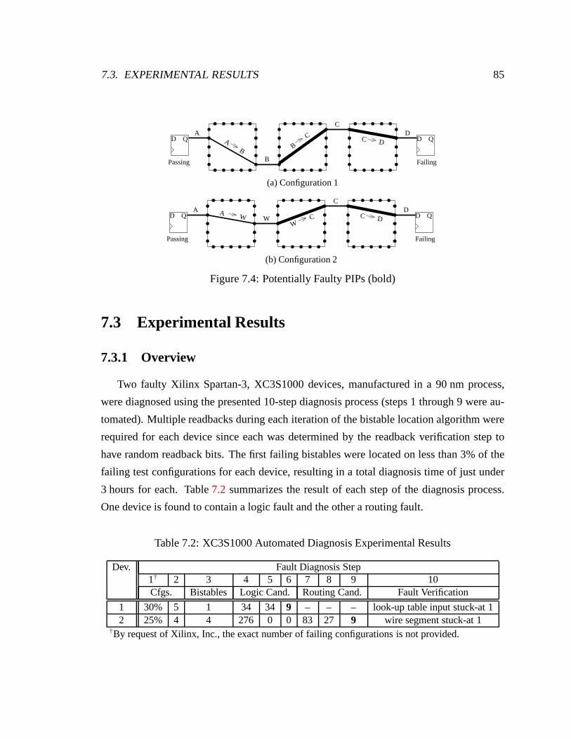
7.3. EXPERIMENTAL RESULTS 85
D Q D QC DAB B
C
B
CDA
Passing Failing
(a) Configuration 1
D Q D QC DWAC
W
CDA
W
Passing Failing
(b) Configuration 2
Figure 7.4: Potentially Faulty PIPs (bold)
7.3 Experimental Results
7.3.1 Overview
Two faulty Xilinx Spartan-3, XC3S1000 devices, manufactured in a 90 nm process,
were diagnosed using the presented 10-step diagnosis process (steps 1 through 9 were au-
tomated). Multiple readbacks during each iteration of the bistable location algorithm were
required for each device since each was determined by the readback verification step to
have random readback bits. The first failing bistables were located on less than 3% of the
failing test configurations for each device, resulting in a total diagnosis time of just under
3 hours for each. Table7.2 summarizes the result of each step of the diagnosis process.
One device is found to contain a logic fault and the other a routing fault.
Table 7.2: XC3S1000 Automated Diagnosis Experimental Results
Dev. Fault Diagnosis Step1† 2 3 4 5 6 7 8 9 10Cfgs. Bistables Logic Cand. Routing Cand. Fault Verification
1 30% 5 1 34 34 9 – – – look-up table input stuck-at 12 25% 4 4 276 0 0 83 27 9 wire segment stuck-at 1
†By request of Xilinx, Inc., the exact number of failing configurations is not provided.
86 CHAPTER 7. AUTOMATED FAULT DIAGNOSIS
7.3.2 Logic Fault Diagnosis
Device 1 failed roughly 30% of the several hundred manufacturing test configurations
(device test, step 1), of which 5 were determined to be usablefor bistable location (read-
back verification, step 2). The same first failing bistable was identified for each test config-
uration (bistable location, step 3), resulting in 34 logic fault candidates (fan-in cone logic
extraction, step 4). After logic fault candidate elimination (steps 5 and 6) only 9 logic fault
candidates remained; therefore, the routing fault steps were skipped and fault verification
(step 10) was conducted.
Eight of the 9 logic fault candidates were stuck-at 0 and stuck-at 1 faults on the 4 address
inputs of a look-up table while the ninth was a stuck-at 1 fault on the write select enable
(ws en) input of the same look-up table. By testing for each logic fault independently (fault
verification, step 10), it was shown that only the ninth faultcandidate is actually a fault.
7.3.3 Routing Fault Diagnosis
Device 2 failed roughly 25% of the several hundred manufacturing test configurations
(device test, step 1), of which 4 were determined to be usablefor bistable location (readback
verification, step 2). Four different first failing bistables were identified (bistable location,
step 3), resulting in 273 logic fault candidates (fan-in cone logic extraction, step 4). Af-
ter logic fault candidate elimination (steps 5 and 6), no logic fault candidates remained;
therefore, it was assumed that the fault being diagnosed is arouting fault.
The fan-in cones of the 4 first failing bistables identified 83routing fault candidates
(fan-in cone PIP extraction, step 7), of which 27 were commonto all bistable-located test
configurations (routing fault commonality, step 8). Only 9 routing fault candidates were not
eliminated by the passing test configurations (routing fault consistency, step 9), yielding a
small set of fault candidates for fault verification.
One interconnect was common to 3 of the 9 potentially-faultyPIPs; therefore, it was
logical to test this interconnect first during fault verification (step 10), which revealed that
it was stuck-at 1. Furthermore, independently testing eachof the other routing fault candi-
dates showed that they did not correspond to actual faults.
7.4. SUMMARY 87
7.4 Summary
Fault diagnosis is important for making manufacturing improvements to increase yield.
Unfortunately, in practice FPGA fault diagnosis isad hoc, requiring days to weeks to di-
agnose a single device. Furthermore, formal diagnosis techniques—those which generate
a set of test configurations to be used for diagnosis—are limited to either a particular type
of fault (logic or routing) or to a particular FPGA architecture and size. The presented
automated fault diagnosis technique makes use of the already existing manufacturing test
configurations by using the readback capability of an FPGA. The advantages are that (1) the
diagnosis time is reduced from days or weeks to only several hours, and (2) the technique
is applicable to any FPGA regardless of architecture or size.

88 CHAPTER 7. AUTOMATED FAULT DIAGNOSIS
This page intentionally left blank.
Chapter 8
Concluding Remarks
Integrated circuit manufacturing is imperfect, resultingin device defects that cause
an FPGA to function incorrectly. A manufacturer must therefore execute two essential
tasks: (1) thorough test to ensure high device quality, and (2) efficient diagnosis to achieve
high manufacturing yield. Although their are many test and diagnosis techniques for non-
configurable circuits like ASICs or microprocessors, most cannot be directly applied to
an FPGA due to its configurability. The configurable interconnection network poses the
primary challenge to FPGA test and diagnosis since numeroussignal paths (hundreds or
more) can be configured between a single pair of logic elements, each of which may be
faulty. The result is that many test configurations (hundreds), each either implementing
a different logic function or a different mapping of the samelogic function to the FPGA,
are required to exercise a sufficient number of these paths for effective test or diagnosis.
Because of the number of test configurations, attempting to test or diagnose an FPGA us-
ing techniques intended for non-configurable circuits is very difficult; many times test or
diagnosis becomes intractable.
Instead of considering the configurability of an FPGA a burden that must be circum-
vented to effectively test or diagnose an FPGA, it can be considered a tool to enhance
test and diagnosis. This dissertation presents several neweffective test and diagnosis tech-
niques that take advantage of the configurability of an FPGA,useful for both application-
independent and application-dependent FPGAs. Three test techniques are presented in
PartII : delay fault test, bridge fault test, and test time reduction. Two diagnosis techniques
are presented in PartIII : bridge fault location and automated stuck-at fault diagnosis.
Delay faults can cause timing failures in an otherwise functioning FPGA; however,
they are difficult to detect due to the slow test speeds of contemporary ATE. In Chap.3 a
technique is developed in which the logic blocks of an FPGA are configured to (1) create
89
90 CHAPTER 8. CONCLUDING REMARKS
controlled signal races on a set of paths under test, and (2) observe the difference in prop-
agation delays between racing signals, making it possible to detect very small delay faults
(nanosecond range) with slow ATE.
Bridge faults occur in deep sub-micron process technologies; however, they are difficult
to detect in an FPGA using Boolean tests due to the NMOS pass transistor implementation
of switch matrices. In Chap.4 a technique is developed in which an FPGA is programmed
with several complimentary test configurations to implement a very effective differential
IDDQ test to detect bridge faults. It is shown that only 5 test configurations are required to
detect all interconnect bridge faults.
To achieve high fault coverage of the interconnection network of an FPGA, hundreds
of test configurations are required; unfortunately, the configuration time is orders of mag-
nitude longer than test vector application and response observation times. In Chap.5 a
modification to the configuration hardware is developed in which the tiled structure of both
an FPGA and each test configuration is used to decrease the configuration time by approxi-
mately 40%. It is shown that very little additional hardwareis required, only several 2-input
multiplexers (R−3 in total for anR×C FPGA).
Fault location is an important part of fault diagnosis sinceit is usually necessary to
locate a fault in order to identify the underlying defect. InChap.6an automated bridge fault
location technique is developed that uses the differentialIDDQ test presented in Chap.4. It
is shown that by iteratively (1) partitioning the nets of a test configuration, (2) testing
the FPGA with each partition independently, and (3) eliminating the nets of the fault-free
partitions, interconnect bridge faults can be located. Because the number of iterations is
logarithmic in the number of nets, the process can be used forvery large FPGAs.
Finally, fault diagnosis is important because the information obtained can be used to
make manufacturing improvements to increase yield; however, current FPGA fault diagno-
sis techniques are both time consuming and limited. In Chap.7 an automated fault diagno-
sis process is developed that takes advantage of the configurability of an FPGA to make use
of the already existing manufacturing test configurations.The advantages are: (1) the diag-
nosis time is reduced from days or weeks (as seen in practice)to only hours, (2) any fault
detectable by the manufacturing test configurations can be diagnosed, and (3) the process
is independent of FPGA architecture and size.
References
[Abramovici et al. 1990] Abramovici, M., Breuer, M., and Friedman, A.,Digital Systems
Testing and Testable Design. IEEE Press, 1990.
[Abramovici and Stroud 2000] Abramovici, M. and Stroud, C.,“BIST-based detection
and diagnosis of multiple faults in FPGAs,”Proc. Int. Test Conf., pp. 785–794, 2000.
[Abramovici and Stroud 2001] Abramovici, M. and Stroud, C.,“BIST-based test and di-
agnosis of FPGA logic blocks,”IEEE Trans. VLSI Systems, pp. 159–172, 2001.
[Abramovici and Stroud 2002] Abramovici, M. and Stroud, C.,“BIST-based delay-fault
testing in FPGAs,”Proc. Eighth IEEE Int. On-Line Testing Workshop, pp. 131–134,
2002.
[Abramovici et al. 1999] Abramovici, M., Stroud, C., Hamilton, C., Wijesuriya, C., and
Verma, V., “Using roving STARs for on-line testing and diagnosis of FPGAs in fault-
tolerant applications,”Proc. Int. Test Conf., pp. 973–982, 1999.
[Chakravarty and Thadikaran 1997] Chakravarty, S. and Thadikaran, P.,Introduction to
IDDQ Testing. Kluwer Academic Publishers, Boston, 1997.
[Chess et al. 1995] Chess, B., Lavo, D., Ferguson, F., and Larrabee, T., “Diagnosis of
realistic bridging faults with single stuck-at information,” Proc. IEEE/ACM Int. Conf.
Computer-Aided Design, pp. 185–192, 1995.
[Chmelar 2003] Chmelar, E., “FPGA interconnect delay faulttesting,” Proc. Int. Test
Conf., pp. 1239–1247, 2003.
[Chmelar 2004a] Chmelar, E., “Automated FPGA fault diagnosis,” CRC TR-04-04, 2004.
[Chmelar 2004b] Chmelar, E., “Subframe multiplexing for FPGA manufacturing test,”
Proc. Int. Symp. FPGAs, 2004.
91
92 REFERENCES
[Chmelar 2004c] Chmelar, E., “Subframe multiplexing: FPGAmanufacturing test time
reduction,”CRC TR-04-01, 2004.
[Chmelar and Toutounchi 2004] Chmelar, E. and Toutounchi, S., “FPGA bridging fault
detection and location via differentialIDDQ,” Proc. 22nd VLSI Test Symp., 2004.
[Das and Touba 1999] Das, D. and Touba, N., “A low cost approach for detecting, locating,
and avoiding interconnect faults in FPGA-based reconfigurable systems,”Proc. 12th Int.
Conf. VLSI Design, pp. 266–269, 1999.
[Doumar and Ito 1999] Doumar, A. and Ito, H., “Testing the logic cells and interconnect
resources for FPGAs,”Proc. Eighth Asian Test Symp., pp. 369–374, 1999.
[Fantini and Morandi 1985] Fantini, F. and Morandi, G., “Failure modes and mechanisms
for VLSI ICs, a review,”Proc. Inst. Electrical Engineering, 132(3):74–81, 1985.
[Ferguson and Larrabee 1991] Ferguson, F. and Larrabee, T.,“Test pattern generation for
realistic bridging faults in CMOS ICs,”Proc. Int. Test Conf., pp. 492–499, 1991.
[Fernandes and Harris 2003] Fernandes, D. and Harris, I., “Application of built-in self test
for interconnect testing of FPGAs,”Proc. Int. Test Conf., pp. 1248–1257, 2003.
[Gattiker and Maly 1996] Gattiker, A. and Maly, W., “Currentsignatures [VLSI circuit
testing],”Proc. 14th VLSI Test Symp., pp. 112–117, 1996.
[Gattiker et al. 1996] Gattiker, A., Nigh, P., Grosch, D., and Maly, W., “Current signatures
for production testing [CMOS ICs],”IEEE Int. Workshop IDDQ Testing, pp. 25–28, 1996.
[Gulati and Hawkins 1992] Gulati, R. and Hawkins, C.,IDDQ Testing of VLSI Circuits.
Kluwer Academic Publishers, Boston, 1992.
[Harris et al. 2001] Harris, I., Menon, P., and Tessier, R., “BIST-based delay path testing
in FPGA architectures,”Proc. Int. Test Conf., pp. 932–938, 2001.
[Harris and Tessier 2000a] Harris, I. and Tessier, R., “Diagnosis of interconnect faults
in cluster-based FPGA architectures,”IEEE/ACM Int. Conf. Computer-Aided Design,
pp. 472–475, 2000.
REFERENCES 93
[Harris and Tessier 2000b] Harris, I. and Tessier, R., “Interconnect testing in cluster-based
FPGA architectures,”Proc. 37th Design Automation Conf., pp. 49–54, 2000.
[Harris and Tessier 2002] Harris, I. and Tessier, R., “Testing and diagnosis of intercon-
nect faults in cluster-based FPGA architectures,”IEEE Trans. Computer-Aided Design
Integrated Circuits, 21:1337–1343, 2002.
[Hawkins et al. 1989] Hawkins, C., Soden, J., Fritzemeier, R., and Horning, L., “Quies-
cent power supply current measurement for CMOS IC defect detection,” IEEE Trans.
Industrial Electronics, 36:211–218, 1989.
[Holfich 1994] Holfich, W.,Using the XC4000 Readback Capability. Xilinx, Inc., San
Jose, CA, 1994.
[Horning et al. 1987] Horning, L., Soden, J., Fritzemeier, R., and Hawkins, C., “Measure-
ment of quiescent power supply current for CMOS ICs in production testing,”Proc. Int.
Test Conf., pp. 300–309, 1987.
[Huang and Lombardi 1996] Huang, W. and Lombardi, F., “An approach to testing pro-
grammable/configurable field programmable gate arrays,”Proc. 14th VLSI Test Symp.,
pp. 450–455, 1996.
[ITRS 2003] ITRS, “International technology roadmap for semiconductors,”
http://public.itrs.net, 2003.
[Krasniewski 2001] Krasniewski, A., “Testing FPGA delay faults in the system environ-
ment is very different from ordinary delay fault testing,”Proc. Seventh Int. On-line Test-
ing Workshop, pp. 37–40, 2001.
[Kusse 1997] Kusse, E., “Analysis and circuit design for lowpower programmable logic
module,” Master’s thesis, Dept. Electical Engineering andComputer Science, Univ. Cal-
ifornia Berkeley, 1997.
[Li et al. 2003] Li, F., Chen, D., He, L., and Cong, J., “Architecture evaluation for power
efficient FPGAs,”Proc. Int. Symp. FPGAs, pp. 175–184, 2003.
94 REFERENCES
[Li et al. 2001] Li, J., Tseng, C., and McCluskey, E., “Testing for resistive opens and stuck
opens,”Proc. Int. Test Conf., pp. 1049–1058, 2001.
[Lu and Chen 2002] Lu, S. and Chen, C., “Fault detection and fault diagnosis techniques
for lookup table FPGAs,”Proc. 11th Asian Test Symp., pp. 236–241, 2002.
[Makar and McCluskey 1996] Makar, S. and McCluskey, E., “Some faults need anIDDQ
test,”Proc. IEEE Int. Workshop IDDQ Testing, pp. 102–103, 1996.
[Maxwell et al. 2000] Maxwell, P., O’Neill, P., Aitken, R., Dudley, R., Jaarsma, N.,
Quach, M., and Wiseman, D., “Current ratios: A self-scalingtechnique for production
testing,”Proc. Int. Test Conf., pp. 1148–1156, 2000.
[McCluskey 1993] McCluskey, E., “Quality and single-stuckfaults,” Proc. Int. Test Conf.,
p. 597, 1993.
[McCluskey et al. 2004] McCluskey, E., Al-Yamani, A., Li, J., Tseng, C., Volkerin, E.,
Ferhani, F., Li, E., and Mitra, S., “ELF-Murphy data on defects and test sets,”Proc.
22nd VLSI Test Symp., pp. 16–22, 2004.
[McCluskey and Tseng 2000] McCluskey, E. and Tseng, C., “Stuck-at fault tests vs. actual
defects,”Proc. Int. Test Conf., pp. 336–342, 2000.
[Miller 1999] Miller, A., “ IDDQ testing in deep submicron integrated circuits,”Proc. Int.
Test Conf., pp. 724–729, 1999.
[Needham et al. 1998] Needham, W., Prunty, C., and Yeoh, E., “High volume micropro-
cessor test escapes, an analysis of defects our tests are missing,” Proc. Int. Test Conf.,
pp. 25–34, 1998.
[Niamat et al. 2002] Niamat, M., Nambiar, R., and Jamali, M.,“A BIST scheme for testing
the interconnects of SRAM-based FPGAs,”45th Midwest Symp. Circuits and Systems,
2:41–44, 2002.
[Poon et al. 2002] Poon, K., Yan, A., and Wilton, S., “A flexible power model for FPGAs,”
Proc. Field-Programmable Logic and Applications, pp. 312–321, 2002.
REFERENCES 95
[Powell et al. 2000] Powell, T., Pair, J., M. St. John, and Counce, D., “DeltaIDDQ for
testing reliability,”Proc. 18th VLSI Test Symp., pp. 439–443, 2000.
[Rajsuman 1994] Rajsuman, R.,IDDQ Testing for CMOS VLSI. Artech House, 1994.
[Renovell et al. 1997a] Renovell, M., Figueras, J., and Zorian, Y., “Test of RAM-based
FPGA: Methodology and application to interconnect,”Proc. 15th VLSI Test Symp.,
pp. 230–237, 1997.
[Renovell et al. 1997b] Renovell, M., Portal, J., Figueras,J., and Zorian, Y., “Test pat-
tern and test configuration generation methodology for the logic of RAM-based FPGA,”
Sixth Asian Test Symp., pp. 254–259, 1997.
[Renovell et al. 1998] Renovell, M., Portal, J., Figueras, J., and Zorian, Y., “Testing the
interconnect of RAM-based FPGAs,”IEEE Design and Test of Computers, pp. 45–50,
1998.
[Renovell et al. 1999a] Renovell, M., Portal, J., Figueras,J., and Zorian, Y., “Minimizing
the number of test configurations for different FPGA families,” Proc. Eighth Asian Test
Symp., pp. 363–368, 1999.
[Renovell et al. 1999b] Renovell, M., Portal, J., Figueras,J., and Zorian, Y., “Test config-
uration minimization for the logic cells of SRAM-based FPGAs: A case study,”Proc.
European Test Workshop, pp. 146–151, 1999.
[Renovell and Zorian 2000] Renovell, M. and Zorian, Y., “Different experiments in test
generation for Xilinx FPGAs,”Proc. Int. Test Conf., pp. 854–862, 2000.
[Shang et al. 2002] Shang, L., Kaviani, A., and Bathala, K., “Dynamic power consumption
in Virtex-II FPGA family,” Proc. Int. Symp. FPGAs, pp. 157–164, 2002.
[Stroud et al. 1996] Stroud, C., Konala, S., Ping, C., and Abramovici, M., “Built-in self-
test of logic blocks in FPGAs (finally, a free lunch: BIST without overhead),”Proc. 14th
VLSI Test Symp., pp. 387–392, 1996.
96 REFERENCES
[Stroud et al. 2001] Stroud, C., Lashinsky, M., Nall, J., Emmert, J., and Abramovici, M.,
“On-line BIST and diagnosis of FPGA interconnect using roving STARs,”Proc. Seventh
Int. On-line Testing Workshop, pp. 27–33, 2001.
[Stroud et al. 2002] Stroud, C., Nall, J., Lashinsky, M., andAbramovici, M., “BIST-based
diagnosis of FPGA interconnect,”Proc. Int. Test Conf., pp. 618–627, 2002.
[Sun et al. 2002a] Sun, X., Alimohammad, A., and Trouborst, P., “Modeling of FPGA
local/global interconnect resources and its derivation ofminimal test configurations,”
Proc. 17th IEEE Int. Symp. Defect and Fault Tolerance, pp. 284–292, 2002.
[Sun et al. 2002b] Sun, X., Xu, J., Alimohammad, A., and Trouborst, P., “Minimal test
configurations for FPGA local interconnects,”Canadian Conf. Computer and Electrical
Engineering, 1:427–432, 2002.
[Sun et al. 2001] Sun, X., Xu, S., Xu, J., and Trouborst, P., “Design and implementation of
a parity-based BIST scheme for FPGA global interconnects,”Canadian Conf. Electrical
and Computer Engineering, pp. 1251–1257, 2001.
[Tahoori 2002a] Tahoori, M., “Diagnosis of open defects in FPGA interconnect,”Proc.
Int. Test Conf., pp. 328–331, 2002.
[Tahoori 2002b] Tahoori, M., “Improving detectability of resistive open defects in FPGA,”
MAPLD Int. Conf., 2002.
[Tahoori 2002c] Tahoori, M., “Testing for resistive open defects in FPGAs,”Proc. IEEE
Int. Conf. Field-Programmable Technology, pp. 332–335, 2002.
[Tahoori 2003] Tahoori, M., “Using satisfiability in application-dependent testing of
FPGA interconnects,”Proc. 40th Design Automation Conf., pp. 678–681, 2003.
[Tahoori and Mitra 2003] Tahoori, M. and Mitra, S., “Automatic configuration generation
for FPGA interconnect testing,”Proc. 21st VLSI Test Symp, pp. 134–139, 2003.
[Tavana et al. 1996] Tavana, D., Yee, W., and Holen, V., “FPGAarchitecture with repeat-
able tiles including routing matrices and logic matrices,”US Patent US05682107, 1996.
REFERENCES 97
[Tavana et al. 1999] Tavana, D., Yee, W., and Holen, V., “FPGAarchitecture with repeat-
able tiles including routing matrices and logic matrices,”US Patent US05883525, 1999.
[Thibeault 1999] Thibeault, C., “On the comparison of∆IDDQ and IDDQ testing,” Proc.
17th VLSI Test Symp., pp. 143–150, 1999.
[Toutounchi et al. 2003] Toutounchi, S., Calderone, A., Ling, Z., Patrie, R., Thorne, E.,
and Wells, R., “Fault emulation testing of programmable logic devices,” US Patent
US6594610B1, 2003.
[Toutounchi and Lai 2002] Toutounchi, S. and Lai, A., “FPGA test and coverage,”Proc.
Int. Test Conf., pp. 599–607, 2002.
[Wang and Huang 1998] Wang, S. and Huang, C., “Testing and diagnosis of interconnect
structures in FPGAs,”Proc. Seventh Asian Test Symp., pp. 283–287, 1998.
[Wang and Tsai 1999] Wang, S. and Tsai, T., “Test and diagnosis of faulty logic blocks in
FPGAs,”IEE Proc. Computers and Digital Techniques, pp. 100–106, 1999.
[Xilinx, Inc. 2001] Xilinx, Inc., Virtex-II Platform FPGA Handbook. Xilinx, Inc., San
Jose, CA, 2001.
[Xilinx, Inc. 2002a] Xilinx, Inc., The Programmable Logic Data Book. Xilinx, Inc., San
Jose, CA, 2002.
[Xilinx, Inc. 2002b] Xilinx, Inc.,Virtex FPGA Series Configuration and Readback. Xilinx,
Inc., San Jose, CA, 2002.
[Xilinx, Inc. 2003a] Xilinx, Inc., Two Flows for Partial Reconfiguration: Module Based
or Difference Based. Xilinx, Inc., San Jose, CA, 2003.
[Xilinx, Inc. 2003b] Xilinx, Inc., Virtex Series Configuration Architecture User Guide.
Xilinx, Inc., San Jose, CA, 2003.
[Xilinx, Inc. 2003c] Xilinx, Inc., “Xilinx easypath solutions,” http://www.xilinx.
com/xlnx/xil prodcatproduct.jsp?title=v2easypath, 2003.
98 REFERENCES
[Yu et al. 1998] Yu, Y., Xu, J., Huang, W., and Lombardi, F., “Adiagnosis method for
interconnects in SRAM based FPGAs,”Proc. Seventh Asian Test Symp., pp. 278–282,
1998.
[Yu et al. 1999] Yu, Y., Xu, J., Huang, W., and Lombardi, F., “Minimizing the number of
programming steps for diagnosis of interconnect faults in FPGAs,” Proc. Eighth Asian
Test Symp., pp. 357–362, 1999.


![Lectures - Department of Computer and Information Science ...TDDD10/lectures/09_automated_planning.pdf · HSP [Bonet & Geffner] FastForward [Hoffmann] Configurable planners 28 Configurable](https://img.pdfslide.net/doc/110x75/5e8853317ae39b5ba96bd4fc/lectures-department-of-computer-and-information-science-tddd10lectures09automated.jpg)