Embed Size (px)
Citation preview
THE UNIVERSITY OF CALGARY
Reconfigurable Antennas Based on Electronically Tunable Reflectarrays
by
Sean Victor Hum
A THESIS
SUBMITTED TO THE FACULTY OF GRADUATE STUDIES
IN PARTIAL FULFILLMENT OF THE REQUIREMENTS FOR THE
DEGREE OF DOCTOR OF PHILOSOPHY
DEPARTMENT OF ELECTRICAL AND COMPUTER
ENGINEERING
CALGARY, ALBERTA
June, 2006
c© Sean Victor Hum 2006

THE UNIVERSITY OF CALGARY
FACULTY OF GRADUATE STUDIES
The undersigned certify that they have read, and recommend to the Faculty of
Graduate Studies for acceptance, a thesis entitled “Reconfigurable Antennas Based
on Electronically Tunable Reflectarrays” submitted by Sean Victor Hum in partial
fulfillment of the requirements for the degree of Doctor of Philosophy.
Supervisor, Dr. Michal OkoniewskiDepartment of Electrical and Com-puter Engineering
Co-supervisor, Dr. Robert J. DaviesDepartment of Electrical and Com-puter Engineering
Dr. Ronald H. JohnstonDepartment of Electrical and Com-puter Engineering
Dr. Gerard LachapelleDepartment of Geomatics Engineer-ing
External Examiner, Dr. John HuangJet Propulsion LaboratoryCalifornia Institute of Technology
Date
ii

Abstract
Reconfigurable antennas have a wide variety of applications in modern communica-
tions systems that require antennas with a dynamically adjustable radiation patterns.
An interesting concept known as a reflectarray antenna has significant potential in
meeting this need if it could be made to be electronically tunable. The design of
such an antenna is the focus of this thesis.
The thesis makes a contribution in several areas related to the design and analy-
sis of electronically tunable reflectarray antennas. First, the thesis presents a design
and modelling technique for a novel reflectarray element exhibiting the phase agility
required in reconfigurable antennas. The models allow the dynamics of the element
to be understood while simultaneously accurately predicting its scattering behav-
iour. Second, the thesis explores the analysis of reflectarrays as a whole, with par-
ticular emphasis on techniques for predicting array-level effects that have not been
previously addressed in detail in the literature. These effects include the specular
reflection behaviour and transient response of reflectarrays.
Finally, the thesis presents several experimental prototypes of reflectarrays based
on the proposed unit cell topology. The measured performance of the antenna cor-
relates very well with theoretical expectations. Experiments with the electronically
tunable reflectarray demonstrate excellent beam-forming characteristics, and vali-
date the concepts and models presented in this thesis.
iii

Acknowledgements
There are many people that have helped make my thesis a wonderful and successful
project, and I would like to take this opportunity to thank them here. First, I would
like to thank my supervisor Michal Okoniewski, who has constantly encouraged me
to strive for excellence in my career. He has been a continual source of inspiration
for me, and has exceeded the call of a supervisor in every possible respect. He is an
exceptional scientist, mentor, and friend. I would also like to thank my co-supervisor
Bob Davies, for all his support and guidance throughout all the many years I have
known him at TRLabs.
I would like to acknowledge several groups and individuals who helped with some
of the technical work in this thesis. I would like to thank the fourth year project
group, consisting of Iris Choi, Saad Rahim, Adrian Wong, and Andrew Sanden,
for their help with constructing the array controller. I would also like to extend
my gratitude to Rob Randall, for all the constructive discussions I had with him
throughout the course of my degree. Additionally, I would like to thank John Shelley
for his technical suggestions which helped make the construction of the array much
easier.
Finally, I would like to acknowledge the National Science and Engineering Re-
search Council of Canada (NSERC), the Alberta Ingenuity Fund (AIF), the Alberta
Informatics Circle of Research Excellence (iCORE), the Association of Universities
and Colleges of Canada (AUCC), the IEEE Antennas and Propagation Society, TR-
Labs, and the University of Calgary, for their financial support.
iv

to Florence,
Simon, Mei Ngan, and Andrew
for all your unconditional love and support

Table of Contents
Approval Page ii
Abstract iii
Acknowledgements iv
Dedication v
Table of Contents vi
List Of Symbols and Abbreviations xiii
1 Introduction 11.1 Candidate Solutions for Reconfigurable Antennas . . . . . . . . . . . 3
1.1.1 Aperture Antennas . . . . . . . . . . . . . . . . . . . . . . . . 31.1.2 Antenna Arrays . . . . . . . . . . . . . . . . . . . . . . . . . . 4
1.2 A Proposal for a Reconfigurable Antenna Platform . . . . . . . . . . 91.3 Thesis Goals . . . . . . . . . . . . . . . . . . . . . . . . . . . . . . . . 121.4 Thesis Outline . . . . . . . . . . . . . . . . . . . . . . . . . . . . . . . 13
2 Background 152.1 Antenna Directivity and Gain . . . . . . . . . . . . . . . . . . . . . . 152.2 Antenna Arrays . . . . . . . . . . . . . . . . . . . . . . . . . . . . . . 19
2.2.1 Basic Principles . . . . . . . . . . . . . . . . . . . . . . . . . . 192.2.2 Two-dimensional Planar Arrays . . . . . . . . . . . . . . . . . 232.2.3 Array Design Considerations and Directivity . . . . . . . . . . 25
2.3 Reflector Antennas . . . . . . . . . . . . . . . . . . . . . . . . . . . . 302.3.1 Principles of Operation . . . . . . . . . . . . . . . . . . . . . . 302.3.2 Radiation Pattern . . . . . . . . . . . . . . . . . . . . . . . . . 332.3.3 Directivity . . . . . . . . . . . . . . . . . . . . . . . . . . . . . 362.3.4 Efficiency . . . . . . . . . . . . . . . . . . . . . . . . . . . . . 38
2.4 Reflectarray Antennas . . . . . . . . . . . . . . . . . . . . . . . . . . 402.4.1 Principle of Operation . . . . . . . . . . . . . . . . . . . . . . 412.4.2 Techniques for Realizing Fixed Reflectarrays . . . . . . . . . . 452.4.3 Tunable Reflectarrays . . . . . . . . . . . . . . . . . . . . . . . 55
vi

3 A Phase-Agile Reflectarray Element 593.1 Proposed Element Design . . . . . . . . . . . . . . . . . . . . . . . . 593.2 Unit Cell Modelling . . . . . . . . . . . . . . . . . . . . . . . . . . . . 64
3.2.1 Equivalent Circuit Model . . . . . . . . . . . . . . . . . . . . . 653.2.2 Computational Electromagnetics Model . . . . . . . . . . . . . 69
3.3 Model Validation . . . . . . . . . . . . . . . . . . . . . . . . . . . . . 723.3.1 Cell Design Details . . . . . . . . . . . . . . . . . . . . . . . . 733.3.2 Equivalent Circuit Parameter Computations . . . . . . . . . . 743.3.3 Model Results . . . . . . . . . . . . . . . . . . . . . . . . . . . 76
3.4 Experimental Measurements of the Unit Cell . . . . . . . . . . . . . . 793.4.1 Fixed Capacitor Cell Results . . . . . . . . . . . . . . . . . . . 823.4.2 Varactor Diode Cell Results . . . . . . . . . . . . . . . . . . . 84
4 Reflectarray Analysis 864.1 Evaluating Reflectarray Gain . . . . . . . . . . . . . . . . . . . . . . 86
4.1.1 Reflectarray Gain . . . . . . . . . . . . . . . . . . . . . . . . . 864.1.2 Element Gain . . . . . . . . . . . . . . . . . . . . . . . . . . . 91
4.2 Infinite Reflectarray Analysis using the FDTD Technique . . . . . . . 924.2.1 Overview of Technique . . . . . . . . . . . . . . . . . . . . . . 944.2.2 Computation of Far-Field Radiation Pattern . . . . . . . . . . 97
4.3 Results of FDTD Reflectarray Simulations . . . . . . . . . . . . . . . 1054.3.1 Reflectarray Scattering Demonstration and Transient Response 1054.3.2 Specular Reflection . . . . . . . . . . . . . . . . . . . . . . . . 109
5 Experimental Reflectarray Designs 1155.1 Overview of Experimental Reflectarray Designs . . . . . . . . . . . . 115
5.1.1 Fixed Reflectarray Design . . . . . . . . . . . . . . . . . . . . 1175.1.2 Electronically Tunable Reflectarray Design . . . . . . . . . . . 119
5.2 Measurement Methodology . . . . . . . . . . . . . . . . . . . . . . . . 1275.2.1 Bistatic Radar Cross Section Measurements . . . . . . . . . . 1285.2.2 Monostatic Radar Cross Section Measurements . . . . . . . . 1305.2.3 Description of Experiments . . . . . . . . . . . . . . . . . . . 1355.2.4 Self-Phasing Control of Reflectarrays . . . . . . . . . . . . . . 137
5.3 Fixed Reflectarray Results . . . . . . . . . . . . . . . . . . . . . . . . 1415.4 Electronically Tunable Reflectarray Results . . . . . . . . . . . . . . . 145
5.4.1 Monostatic RCS Experiment with Open-Loop Control . . . . 1455.4.2 Monostatic RCS Experiment with Self-Phasing Control . . . . 1505.4.3 Bistatic RCS Experiment with Open-Loop Control . . . . . . 1525.4.4 Bistatic RCS Experiment with Self-Phasing Control . . . . . . 158
5.5 Closing Remarks . . . . . . . . . . . . . . . . . . . . . . . . . . . . . 160
vii

6 Recent Developments and Future Work 1636.1 Possible Reflectarray Element Improvements . . . . . . . . . . . . . . 163
6.1.1 Reflectarray Element Linearity . . . . . . . . . . . . . . . . . 1646.1.2 A Proposal for a MEMS Reflectarray Element . . . . . . . . . 1706.1.3 Other Cell Possibilities . . . . . . . . . . . . . . . . . . . . . . 175
6.2 Future Work at the Array Level . . . . . . . . . . . . . . . . . . . . . 1786.2.1 Alternative Reflectarray Geometries . . . . . . . . . . . . . . . 1786.2.2 Further Investigation of the Self-Phasing Controller . . . . . . 179
7 Conclusions 1817.1 Research Achievements . . . . . . . . . . . . . . . . . . . . . . . . . . 1817.2 Thesis Contributions . . . . . . . . . . . . . . . . . . . . . . . . . . . 1847.3 Closing Remarks . . . . . . . . . . . . . . . . . . . . . . . . . . . . . 186
Bibliography 187
A Description of Genetic Algorithm Implementation 200
viii

List of Tables
3.1 Equivalent circuit parameters for various substrate heights . . . . . . 77
4.1 FDTD parameters used in infinite reflectarray simulation . . . . . . . 1054.2 Varactor diode capacitances required to form 4-element phase gradient 1064.3 Varactor diode capacitances required to create oppositely-phased unit
cells . . . . . . . . . . . . . . . . . . . . . . . . . . . . . . . . . . . . 112
5.1 Design parameters of the two experimental reflectarray designs . . . . 1165.2 Distribution of capacitor pairs in the fixed reflectarray design . . . . . 1185.3 Fixed reflectarray design (all capacitor values in pF) . . . . . . . . . . 1185.4 Beamwidth of the feed horn at 5.8 GHz . . . . . . . . . . . . . . . . . 1255.5 Aperture efficiencies and sub-efficiencies of the offset feed . . . . . . . 1275.6 Loss budget for retro-directive configuration (θr = 80, φr = 20) . . . 1505.7 Loss budget for bistatic configuration (θb = 83.5, φb = 20) . . . . . . 1555.8 Hypothetically improved loss budget for bistatic configuration (θb =
83.5, φb = 20) . . . . . . . . . . . . . . . . . . . . . . . . . . . . . . 161
ix

List of Figures
1.1 A generic antenna array . . . . . . . . . . . . . . . . . . . . . . . . . 61.2 Reflector antennas . . . . . . . . . . . . . . . . . . . . . . . . . . . . 11
2.1 Radiation intensity of an arbitrary antenna . . . . . . . . . . . . . . . 162.2 An array of isotropic antenna elements . . . . . . . . . . . . . . . . . 202.3 An array of isotropic antenna elements, narrowband case . . . . . . . 222.4 Geometry of a two-dimensional planar array . . . . . . . . . . . . . . 242.5 Coordinate system for a parabolic reflector . . . . . . . . . . . . . . . 312.6 Cross section of a parabolic reflector . . . . . . . . . . . . . . . . . . 322.7 A generalized reflectarray . . . . . . . . . . . . . . . . . . . . . . . . 412.8 Cross section of a reflectarray . . . . . . . . . . . . . . . . . . . . . . 422.9 Reflection phase from a variable-size patch . . . . . . . . . . . . . . . 48
3.1 Frequency agile antenna based on a shunt tuning diode . . . . . . . . 613.2 Frequency agile antenna tuning characteristics . . . . . . . . . . . . . 623.3 Reflectarray cell topology . . . . . . . . . . . . . . . . . . . . . . . . 633.4 Infinite array scattering scenario . . . . . . . . . . . . . . . . . . . . . 653.5 Equivalent circuit for predicting scatter from an unmodified microstrip
patch . . . . . . . . . . . . . . . . . . . . . . . . . . . . . . . . . . . . 663.6 Introducing a gap discontinuity . . . . . . . . . . . . . . . . . . . . . 683.7 Modelling current crowding effects . . . . . . . . . . . . . . . . . . . . 693.8 Introducing varactor diodes into the circuit model . . . . . . . . . . . 703.9 Simplified equivalent circuit . . . . . . . . . . . . . . . . . . . . . . . 713.10 Parallel-plate waveguide setup for FDTD simulations . . . . . . . . . 723.11 Fringing capacitance simulation . . . . . . . . . . . . . . . . . . . . . 753.12 Comparison of equivalent circuit model to FDTD simulations . . . . . 783.13 Comparison of equivalent circuit model to FDTD simulations for two
Rv values . . . . . . . . . . . . . . . . . . . . . . . . . . . . . . . . . 803.14 Reflectarray unit cell inside rectangular waveguide . . . . . . . . . . . 813.15 Experimental characterization of unit cells using rectangular waveguide 823.16 Comparison of measured and FDTD-simulated unit cell scattering
results . . . . . . . . . . . . . . . . . . . . . . . . . . . . . . . . . . . 833.17 Measured unit cell scattering from the varactor-diode based cell . . . 84
4.1 Radiation pattern of a microstrip patch . . . . . . . . . . . . . . . . . 934.2 A section of an infinite reflectarray . . . . . . . . . . . . . . . . . . . 964.3 Evolution of the scattered field from the reflectarray . . . . . . . . . . 1084.4 Angular spectrum of the simulated sub-array . . . . . . . . . . . . . . 110
x

4.5 Specular reflection as a function of unit cell size . . . . . . . . . . . . 113
5.1 Coordinate system used for reflectarray design and measurements . . 1175.2 Photo of completed fixed reflectarray surface . . . . . . . . . . . . . . 1195.3 Scattering characteristics of 5.8 GHz unit cell design . . . . . . . . . . 1205.4 Setup of tunable reflectarray layout . . . . . . . . . . . . . . . . . . . 1215.5 Photo of completed electronically tunable reflectarray surface . . . . . 1225.6 Screen shot of the electronically tunable reflectarray control program 1235.7 Feed horn used for scanning the reflectarray . . . . . . . . . . . . . . 1245.8 Directivity of the feed horn at 5.8 GHz . . . . . . . . . . . . . . . . . 1255.9 Offset feed geometry for a reflectarray . . . . . . . . . . . . . . . . . . 1265.10 Feed illumination on the reflectarray (contours in dB) . . . . . . . . . 1285.11 Measurement setup of a bistatic RCS experiment (positioning control
system not shown) . . . . . . . . . . . . . . . . . . . . . . . . . . . . 1295.12 Measurement setup of a monostatic RCS experiment (positioning con-
trol system not shown) . . . . . . . . . . . . . . . . . . . . . . . . . . 1315.13 Model of an ideal reflectarray . . . . . . . . . . . . . . . . . . . . . . 1335.14 A self-phasing reflectarray in receive mode . . . . . . . . . . . . . . . 1385.15 Measured and simulated monostatic RCS of the fixed reflectarray, θ =
100.5 . . . . . . . . . . . . . . . . . . . . . . . . . . . . . . . . . . . 1415.16 Measured and simulated monostatic RCS of the fixed reflectarray, φ =
−12.0 . . . . . . . . . . . . . . . . . . . . . . . . . . . . . . . . . . . 1425.17 Measured monostatic RCS of the electronically tunable reflectarray
surface at θ = 80 . . . . . . . . . . . . . . . . . . . . . . . . . . . . . 1475.18 Monostatic RCS of the φr = 20 reflectarray configuration measured
at θ = 80 . . . . . . . . . . . . . . . . . . . . . . . . . . . . . . . . . 1485.19 Comparison of measured monostatic RCS of the φr = 20 reflectarray
configuration at θ = 80 . . . . . . . . . . . . . . . . . . . . . . . . . 1515.20 Feed scanning setup for bistatic RCS measurements . . . . . . . . . . 1535.21 Bistatic RCS of the several reflectarray configurations measured at
θ = 83.5 . . . . . . . . . . . . . . . . . . . . . . . . . . . . . . . . . . 1545.22 Measured bistatic RCS and cross-polarization for 3 reflectarray con-
figurations at θ = 83.5 . . . . . . . . . . . . . . . . . . . . . . . . . . 1565.23 Frequency dependence of the reflectarray radiation pattern . . . . . . 1575.24 Comparison of measured bistatic RCS of the φd = 20 reflectarray
configuration at θ = 83.5 . . . . . . . . . . . . . . . . . . . . . . . . 159
6.1 Experimental setup of two-tone test . . . . . . . . . . . . . . . . . . . 1676.2 3rd order IMD generated by the reflectarray element . . . . . . . . . 1686.3 5th order IMD generated by the reflectarray element . . . . . . . . . 169
xi

6.4 Output spectrum of reflected signal at 18 dBm input power, 10 V bias 1706.5 Structure of the MEMS capacitor (figure courtesy Greg McFeetors) . 1726.6 Photograph of the integrated MEMS reflectarray cell and components 1736.7 Measured scattering characteristics of the MEMS reflectarray cell . . 1746.8 Conceptual drawing of a transmit-array geometry . . . . . . . . . . . 179
A.1 GA chromosome structure . . . . . . . . . . . . . . . . . . . . . . . . 200
xii

List Of Symbols and Abbreviations
α inter-element phase shift / absolute element phase shift
αi angle of incidence
αr angle of reflection
βeff effective phase constant
Γ reflection coefficient
δ Dirac delta function
∆t FDTD time step size
∆x FDTD grid size in x-direction
∆y FDTD grid size in y-direction
∆z FDTD grid size in z-direction
ε efficiency / electric permittivity
εφ phase error efficiency
εa achievement efficiency
εap aperture efficiency
εblk feed blockage efficiency
εcr cross-polarization efficiency
εr relative permittivity (dielectric constant)
εs spillover efficiency
εt illumination taper efficiency
η intrinsic impedance of free space
θ elevation angle from z-axis
xiii

θ0 desired elevation angle
θb bistatic RCS elevation angle
θf reflector feed angle
θinc incident elevation angle
θi feed horn illumination angle
θinc rectangular waveguide incident angle
θr retro-directive elevation angle
θE E-plane half-beamwidth
θH H-plane half-beamwidth
λ0 wavelength in free space
λc rectangular waveguide cutoff wavelength
µ0 permeability of free space
ξ phase shift applied to an antenna array element
ρ distance from focal point to point on reflector
τ spatial delay from plane wave
φ azimuth angle from x-axis
φ0 desired azimuth angle
φb bistatic RCS azimuth angle
φinc incident azimuth angle
φr retro-directive azimuth angle
ψ reflectarray element phase shift
Ω solid angle
ΩA beam solid angle
xiv

a edge of reflector / rectangular waveguide width /
periodic waveguide width
A vector magnetic potential
Ae effective area of an antenna
Ap physical area of an aperture antenna
AF array factor
AFr array factor of reflectarray
b rectangular waveguide height / periodic waveguide width
c speed of light in free space
C capacitance
Cf fringing capacitance of microstrip patch antenna
Cs series capacitance
Cp parallel capacitance
Cv capacitance of varactor diode
Cmax maximum varactor diode capacitance
Cmin minimum varactor diode capacitance
d antenna array element spacing
D directivity / distance from plane wave to antenna
element / reflector diameter
dB decibel
xv

dBi decibel with respect to an isotropic source
Dmaxe maximum element directivity
Dreflector directivity of a reflector
E electric field
Ea aperture electric field
Einc incident electric field
Er (specular) reflected electric field
ERA far-field electric field from a reflectarray
Es scattered electric field
Esum sum of scattered and reflected electric fields
ESPAR electronically steerable passive array radiator
f frequency
f0 reflectarray design frequency
f1 two-tone test input frequency 1
f2 two-tone test input frequency 2
F normalized antenna factor / reflector focal point
F vector electric potential
FA normalized array factor
Fe normalized element factor
Ff feed antenna pattern factor
FTOTAL total antenna factor for antenna arrays
xvi

FDTD finite-difference time-domain
g gap width in microstrip patch
G gain
Ge element gain
Gmaxe maximum element gain
Gmax maximum antenna gain
Gr reflectarray gain
GA genetic algorithm
GaAs gallium arsenide
GPIB general purpose instrumentation bus
h substrate height
H magnetic field
Ha aperture magnetic field
IMD intermodulation distortion
IM3 third order IMD
IM5 fifth order IMD
Js equivalent electric surface current
k wavenumber in rectangular waveguide
xvii

k0 wavenumber in free space
L microstrip patch length
L Fourier Transform of equivalent magnetic surface current
Lc current crowding inductance
Lv packaging inductance of varactor diode
M number of array elements in E-plane
Ms equivalent magnetic surface current
MEMS micro-electro-mechanical systems
N Number of elements in an array / number of elements in H-plane
N Fourier Transform of equivalent electric surface current
NT number of FDTD time steps
Nx number of FDTD cells in x-direction
Ny number of FDTD cells in y-direction
Nz number of FDTD cells in z-direction
P power
P Fourier Transform of aperture electric field
PEC perfect electric conductor
PPWG parallel plate waveguide
Q Fourier Transform of aperture magnetic field
xviii

r radial distance from antenna / received signal at antenna
rf distance to reflector
R reflectivity
Ri total distance from reflector to feed horn
Rr radiation resistance of a microstrip patch antenna
Rv resistance of varactor diode RLC circuit
RADAR radio detection and ranging
RCS radar cross section
RCSb monostatic RCS
RCSm monostatic RCS
RF radio frequency
RWG rectangular waveguide
tan δ loss tangent
T time delay of true-time-delay device
TEM transverse electromagnetic
TRM transmit-receive module
u angular frequency
u0 fundamental angular frequency
U radiation intensity
Uavg average radiation intensity
xix

Um maximum radiation intensity
VNA vector network analyzer
W microstrip patch width
Xf feed horn displacement in x-direction
Zc impedance of a microstrip transmission line
Zf location of reflector apex /
feed horn displacement in z-direction
xx

Chapter 1
Introduction
“Three years ago, electromagnetic waves were nowhere. Shortly after-
ward, they were everywhere.” — Sir Oliver Heaviside, 1891.
Referring to Hertz’s infamous physical demonstration of the existence of radio
waves in 1888, Heaviside aptly foreshadows the modern era where life with-
out wireless communication seems unimaginable. Today, communication with radio
waves permeates our entire society and culture, and new applications for wireless
devices continue to abound in the modern age. Indeed, waves are everywhere.
The key component of all modern radio communication systems remains the same
as it was in Hertz’s own experiment almost 120 years ago. The antenna, which forms
the physical interface between the hardware of the communications system and the
transmission medium of the radio channel, has evolved considerably from the simple
“Hertzian” dipole Hertz used in his experiments. As communication systems have
evolved and grown in complexity, so have the demands on the antenna itself. The
modern antenna is expected to conform to many specifications such as size, shape,
weight, frequency, bandwidth, functionality, and increasingly, aesthetics.
One of the most important antenna specifications is the gain of the antenna,
which describes how sensitive the antenna is to radiation in a particular direction
compared to an isotropic source. Utilizing directional antennas in a wireless link
relaxes amplifier gain requirements because signal gain is provided by the the focusing

Introduction 2
effect of the antenna. Furthermore, directional antennas can reduce the effect of
interference from directions other than the preferred direction of the antenna.
Many communications systems make use of directional antennas. Some commer-
cial applications using directional antennas include residential television broadcast
systems, fixed point-to-point microwave links, cellular base stations, and wireless
local area networks. A number of these systems, particularly fixed microwave links,
use highly directional antennas with substantial gain. Other systems that use high-
gain antennas include include RADAR systems, satellite communication systems,
deep-space communication systems, and radio telescopes. Often, antennas for high-
gain applications are designed so that their radiation patterns are fixed. Examples
of high-gain antennas include reflector antennas and multi-element antennas such as
Yagi antennas. However, the same applications can often benefit from making the
beam from the antenna adjustable. In RADAR systems, beam scanning is necessary
to track mobile targets, or to scan a physical area for targets. In point-to-point
communication links where one or both of the terminals are mobile (particularly in
satellite communications systems), the beams of both antennas must track with the
movement of the terminals so that adequate communications quality is maintained.
For antennas with a fixed main beam, the only way to introduce such adaptability
is to mechanically steer the antenna. Indeed, this is approach taken with many of
the systems mentioned.
Obviously, mechanical scanning has limitations in terms of tracking speed and
flexibility. Furthermore, there are many applications that benefit from making the
entire beam pattern itself adjustable. Some systems, particularly those operating in a
multipath environment, benefit from antennas capable of forming multiple beams in

1.1 Candidate Solutions for Reconfigurable Antennas 3
the radiation pattern to coherently combine signals emanating from reflectors in the
environment. Other applications, such as smart antennas, rely on being able to form
nulls in the radiation pattern directed in specific directions to cancel interference.
Clearly, such a degree of adaptability in the radiation pattern cannot be achieved
with mechanical scanning, and requires a completely different type of antenna system
altogether.
Antennas that are capable of adjusting their own radiation characteristics are
termed reconfigurable antennas, though the term is broad and does extend to an-
tennas that can change their other parameters such as frequency of operation, band-
width, and so on. Given the breadth of applications that can benefit from reconfig-
urable radiation patterns, the focus of this study is on antennas capable of adapting
their radiation patterns and the term “reconfigurable antenna” refers to such an
antenna.
1.1 Candidate Solutions for Reconfigurable Antennas
Various antenna types can be considered as potential candidates for reconfigurable
antennas. Since the goal is to outfit a high-gain antenna with this functionality,
there are basically two broad classes of antennas that can potentially fill this need:
aperture antennas and antenna arrays.
1.1.1 Aperture Antennas
Aperture antennas are a class of antennas that realize a high amount of gain through
the use of a physical aperture which directly determines the effective aperture of

1.1 Candidate Solutions for Reconfigurable Antennas 4
the antenna. Well-known examples of aperture antennas include horn antennas, and
reflector antennas such as parabolic dishes. Reflector dishes in particular are capable
of realizing immense amounts of gain because the maximum gain of the antenna is
only limited by the physical size of the reflector. The shape of the reflector also
allows for some flexibility in the beam pattern as it can be contoured to produce the
desired beam shape. Indeed, this approach has been used to produce shaped-beam
coverage for satellite applications to ensure the maximum power from satellite is
delivered to continental land masses and not wasted by illuminating oceanic areas.
Aperture antennas, in general, are not easily made reconfigurable. Horns and
reflectors offer little flexibility in adjusting the beam pattern because they are made
from conductors of fixed shape and size. The beam pattern from a reflector can be
selected by using more than one feed antenna or through the use of a mechanically
scanned feed horn mounted over a spherical reflector. Reflectors can also be deformed
to some degree to make beam corrections, and this approach has been utilized to
correct for aberrations in astronomy-based optical systems [1]. However, the degree
to which the reflector can be deformed is very low, allowing for only minute changes
to the beam pattern.
1.1.2 Antenna Arrays
Antenna arrays, as the name suggests, consist of a number of antenna elements
assembled together to form a larger antenna system. There are two subclasses of
antenna arrays: arrays where each element is actively driven by independent radio-
frequency (RF) sources, and arrays where only one of the elements is driven and
the rest of the elements act as parasitic elements. An example of the latter type

1.1 Candidate Solutions for Reconfigurable Antennas 5
of array is the classic Yagi-Uda antenna. This antenna realizes a directional beam
pattern by using well-placed directors and reflectors in close proximity to the driven
element. This produces a highly focused array pattern leading to substantial gain.
These two types of arrays differ quite significantly in their construction since arrays
based on parasitic elements tend to place the elements in the near field of the driven
element (small fractions of a wavelength away), whereas arrays based on actively
driven elements tend to be built such that the elements are separated by a significant
distance (typically a half-wavelength or more).
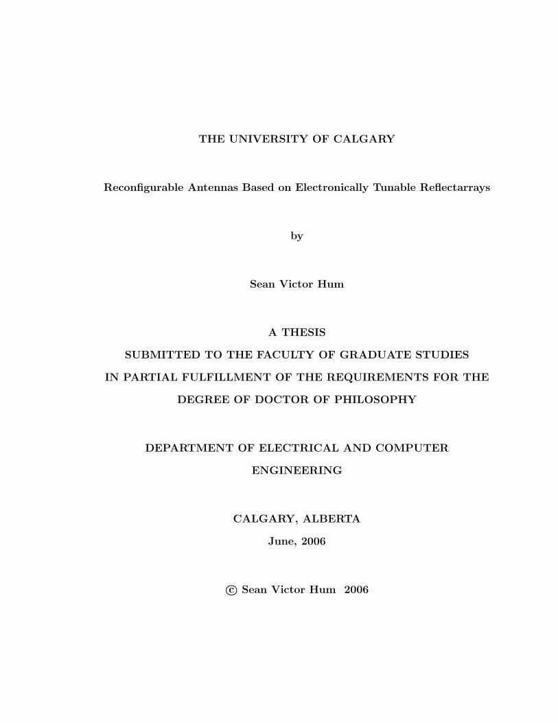
A general diagram of an antenna array utilizing actively driven elements is shown
in Figure 1.1(a). It consists of a number of radiators, each driven by a signal whose
amplitude and phase are controlled independently [2]. Through manipulating the
amplitude weighting and phase shift applied to each of the elements, beams can be
formed and steered by the array. The electrical operation of an antenna array is
discussed in more detail in Chapter 2.
The amount of gain realized from the array can be increased by simply increasing
the number of elements in the array. Often, when the array operates in a receiving
mode as shown in the figure, there is some form of closed-loop control that adjusts
the weighting of the antenna signals so that the desired beam shape is produced.
Metrics extracted from the received signal after the combiner are used to control the
amplitude and phase of the signals from the elements so that optimal performance
from the array is achieved. This is performed by an array controller as shown in the
figure.
The diagram in Figure 1.1(b) shows an alternative realization whereby signals
from the array are collected at an intermediate frequency (IF). This is done so that
1.1 Candidate Solutions for Reconfigurable Antennas 6
CONTROL
...
AMPLITUDE / PHASESHIFTER
RX / TX
Σ
(a) RF beam-former
CONTROL
SOFTWARE...
AMPLITUDE / PHASESHIFTER
RX / TX
Σ
(b) IF beam-former
Figure 1.1: A generic antenna array
phase shifting and amplitude weighting can be done at lower frequencies, which can
reduce costs. More frequently, however, this is done so that operations that were
traditionally implemented at radio frequencies (namely phase shifting and amplitude
weighting) can be performed digitally in software through transforming the analog
IF signals to digital signals using analog-to-digital converters. The point at which
analog-to-digital conversion takes place is denoted by the dashed line in Figure 1.1(b).
The proliferation of digital signal processors has allowed many operations that were
previously realized in the analog domain to be performed digitally, allowing the
control systems to be more tightly integrated with the operations and reducing some
of the cost of the platform. Multiple-beam systems can be easily created and tracked
with the architecture shown in Figure 1.1(b), by introducing additional weighted
sums to the system.
Antenna arrays are natural candidates for reconfigurable antennas because of
their inherent flexibility. This is most obvious in the case of the actively-driven array

1.1 Candidate Solutions for Reconfigurable Antennas 7
shown in Figures 1.1(a) and (b) because the amplitude and phase of each element can
be manipulated at will to produce the desired beam pattern. Reconfigurable beam
patterns can also be achieved with parasitically-loaded arrays. By adjusting the
loading of the parasitic elements, and choosing appropriate positions for them around
the driven element, a large degree of beam reconfigurability can be achieved. A novel
concept known as the electronically steerable passive array radiator (ESPAR) is one
example of such an implementation [3]. Generally, arrays based on actively driven
elements offer the most flexibility for reconfigurable antenna platforms. The reason
for this is that the gain scales with the number of elements, unlike parasitically-
loaded arrays where there is diminishing returns in terms of gain as the number of
parasitic elements is increased. We therefore focus our attention on actively driven
antenna arrays in the upcoming discussion.
Antenna arrays, despite their great potential as reconfigurable antenna platforms,
possess a number of major shortcomings that makes the deployment of reconfigurable
antennas based on the classic array implementation impractical and inexpensive.
These include the following:
1. Cost of RF hardware. Antenna arrays, regardless of whether they are im-
plemented as shown in Figure 1.1(a) or (b), require a substantial amount of
RF hardware. The implementation shown in Figure 1.1(a) requires a separate
RF phase shifter for each antenna element, plus an amplitude controller if am-
plitude weighting is to be used as well. These components tend to be costly
and bulky, increasing the size of the array platform and making it more expen-
sive. The implementation of Figure 1.1(b), while eliminating the need for the

1.1 Candidate Solutions for Reconfigurable Antennas 8
RF phase shifters and amplitude controllers, nevertheless requires a substan-
tial amount of RF hardware in the form of frequency conversion equipment,
filters, and so on. The complexity of these systems increases when they are
used in both transmit and receive modes, where additional components such as
amplifier chains, RF switches, and other components are required. These com-
ponents are generally assembled into a unit called a transmit-receive module
(TRM). In antenna arrays, TRMs must be duplicated for each of the antenna
elements in the system. At high frequencies, these components still tend to
be very expensive, especially components designed for use at millimetre-wave
frequencies where this project is ultimately targeted. This makes antenna ar-
rays generally a costly proposition. Indeed the cost of the RF hardware in
antenna arrays has prevented them from being widely deployed, even at lower
RF frequencies.
2. Feeding difficulties associated with large arrays. Antenna arrays require
that each element is actively fed by an RF signal. For small arrays, this is
usually not a problem, but for large arrays, feeding the array can become a
logistical nightmare. However, a more problematic issue is loss in the feed
network itself, which is a particular problem at high frequencies. The large
number of feed networks required for large high-gain arrays compounds the
loss problem, producing an upper limit on the realizable gain from the array.
Additionally, the feed network is often a source of cross-polarization in planar
antenna arrays.
Any reconfigurable antenna platform based on antenna arrays must therefore

1.2 A Proposal for a Reconfigurable Antenna Platform 9
adequately address these issues if it is to be practically usable in a modern commu-
nication system. An additional issue to be considered is the system used to control
the amplitude and phase of the elements in the array (or purely the phase in the
case of phase-only control). Antenna arrays usually require sophisticated control
algorithms for this purpose. Feedback is often implemented in the form of training
sequences used to provide the controller with a known reference to adjust the element
weights so that the desired metric is optimized. The algorithm used to optimize the
antenna element weights often requires sophisticated processing, especially for large
arrays. The control system, therefore, is an additional issue to be considered when
designing a reconfigurable antenna platform.
1.2 A Proposal for a Reconfigurable Antenna Platform
Due to their flexibility and gain scalability, antenna arrays have prevailed as the
platform for producing adaptable, flexible beam patterns. Antenna arrays can be
found in widespread use for this purpose in phased-array RADAR systems, diversity
antenna systems, and smart antennas. Antenna arrays are therefore a natural choice
as the foundation for any reconfigurable antenna platform. Unfortunately, the design
of a large antenna array is complicated by issues of cost, complexity, and loss, as
discussed in the previous section. Indeed, it is the shortcomings of traditional array
architectures that form bulk of the motivation of this research project.
By contrast, reflectors have none of the cost, complexity, and loss of antenna
arrays but lack in reconfigurability. Therefore, what is proposed is the marriage
of concepts from both reconfigurable antenna arrays and reflector antennas. Both

1.2 A Proposal for a Reconfigurable Antenna Platform 10
platforms offer unique advantages that if combined in a mutually inclusive way, could
provide an attractive reconfigurable antenna platform with regards to performance
and cost. Indeed, the best of both worlds would be offered by the resulting platform.
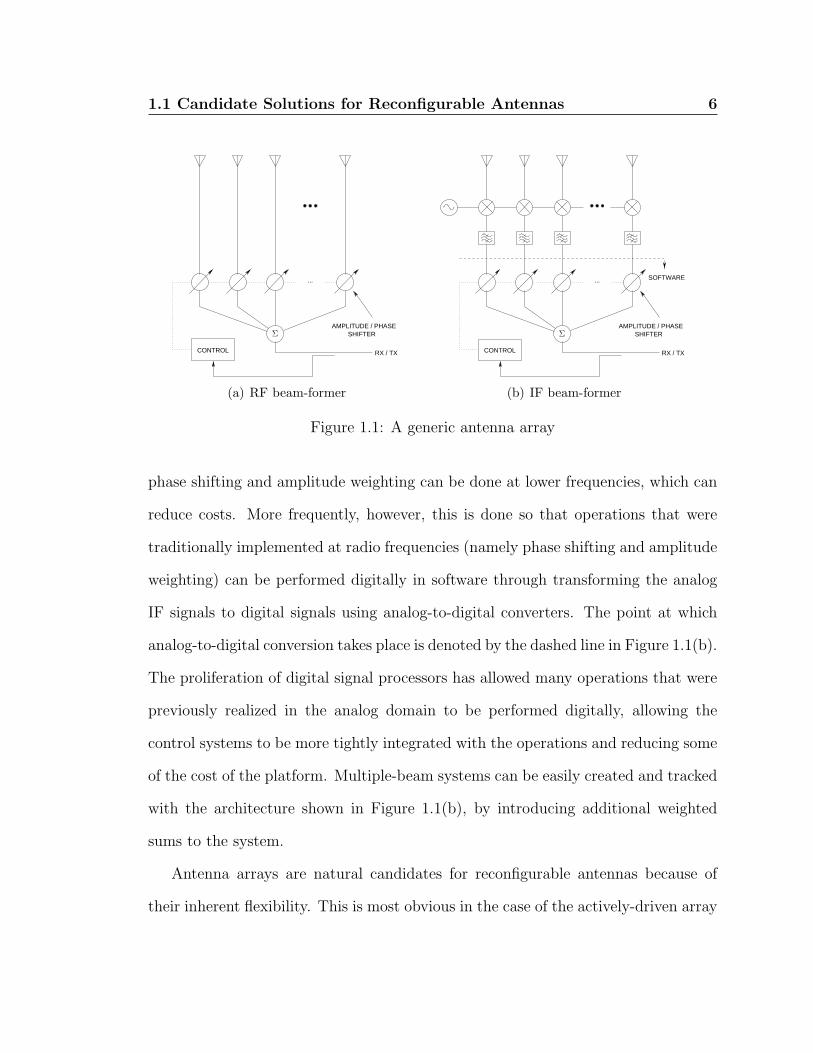
Such a platform does exist in fixed (i.e. non-reconfigurable) form, and is known
as a reflectarray antenna [4]. In recent years, the reflectarray antenna has evolved
into an attractive candidate for applications requiring high-gain, low-profile reflector
antennas. As the name suggests, the reflectarray is a cross between a reflector
antenna and an antenna array. A basic reflectarray antenna resembles a classical
reflector antenna such as the one shown in Figure 1.2(a). Like a reflector antenna,
it is composed of a reflecting surface which is illuminated by a spatial feed such
as a horn antenna. The difference is that the reflector is replaced with a planar
array of microstrip elements (e.g. patches), as shown in Figure 1.2(b). Phasing of
the scattered field to form the desired beam pattern is achieved by modifying the
physical, printed characteristics of the individual elements composing the array, so
that it accurately emulates the behaviour of a parabolic (or similar) reflector. A
discussion for the techniques by which this is done is deferred until Chapter 2, but
it suffices to say a variety of approaches investigated in recent decades allows the
reflectarray to compete with modern reflectors in terms of performance.
Most reflectarrays have been proposed as a planar replacements for bulkier reflec-
tor antennas because of their lower profile, their ability to conform to surfaces, and
their superior cross-polarization characteristics. However, the one untapped capabil-
ity of the reflectarray that few authors have considered is the possibility of making
the beam pattern dynamic using reconfigurable array elements in the place of fixed
elements. Indeed, the reflectarray antenna holds significant promise as a platform
1.2 A Proposal for a Reconfigurable Antenna Platform 11
(a) A parabolic reflector (b) A microstrip reflectarray
Figure 1.2: Reflector antennas
for a reconfigurable antenna array because the unique blend of concepts from both
reflector antennas and antenna arrays yields a unique platform that addresses many
of the shortcomings of each antenna type individually. If the reflector could be made
electronically tunable, it would address all of the shortcomings of antenna arrays
presented earlier. Key features of this platform would include:
1. Spatial feeding. Reflectarrays address loss and logistical issues with conven-
tional RF feed networks for antenna arrays, since the feed network is done away
with altogether. Instead, feeding of each antenna is performed by a secondary
feeding antenna, which illuminates each and every antenna element using free
space as the distribution network. This is the principle upon which classical
reflector antennas operate: feeding of the reflector from a secondary feeding
antenna.
2. Low-cost antenna elements. The antenna array consists of special antenna

1.3 Thesis Goals 12
elements that are capable of modifying their own radiation characteristics,
namely, the phase of their radiated field. Hence, the phase shifting operation
is internalized to the antenna itself, leading to a cost and space savings for each
antenna element. Furthermore, only one TRM in the entire system is needed,
at the feed horn.
3. Amenability to array processing. The system is amenable to a closed-loop
type of control system like that shown in Figure 1.1(a). Since the processing
is done at radio frequencies, the effect of modifying antenna element phasing
is directly observable at the feed horn, which potentially simplifies the control
technique because further processing on the received signal is not necessary.
1.3 Thesis Goals
The analysis and design of a reconfigurable reflectarray is the focus of this thesis.
The goal of the thesis is to not only expand the state-of-the-art in the area of reflec-
tarrays and reconfigurable antennas, but also to demonstrate novel ways in which RF
technology can be integrated with antennas to achieve this adaptability. Specifically,
for this thesis, the investigation aims to make a contribution in three major areas:
1. The development of an electronically tunable reflectarray element exhibiting
the necessary phase agility to add reconfigurability to reflectarrays, which does
not currently exist in the literature. In conjunction with this goal, physical
insight into the electrical operation of such an element is sought, so that the
state-of-the-art in this area can not only be expanded, but well-understood so
that electronically tunable reflectarrays can be designed in a more systematic,

1.4 Thesis Outline 13
and less ad-hoc, fashion.
2. A greater understanding of the dynamics of the system when multiple ele-
ments, particularly electronically tunable ones, are assembled into a reflectar-
ray. There are numerous mechanisms for loss in reflectarrays, and one that
could be better understood is specular reflection loss. The impacts of the
design of the newly-derived tunable elements on this form of loss should be
well-understood.
3. Demonstration of the successful design of an electronically tunable reflectarray
through the realization of an experimental prototype. The successful design of
such a system is seen as the ultimate manifestation of useful design knowledge
generated in this area. The resulting prototype should demonstrate flexible
beam-forming while maintaining predictable and acceptable levels of efficiency.
These goals are realized through the design, analysis, and construction of elec-
tronically tunable reflectarray elements and systems. Physical experiments are used
to validate theoretical models and concepts and ultimately demonstrate a system
that is competitive with the performance and cost of antenna arrays in use today.
1.4 Thesis Outline
The structure of the thesis is as follows. Chapter 2 provides the necessary background
in terms of the theory behind antenna arrays and reflectors on which the reflectarray
concept is based. It also provides a presentation of the state-of-the-art with respect
to reflectarrays and tuning techniques.

1.4 Thesis Outline 14
Chapter 3 describes the design of a phase agile reflectarray antenna element in
detail. Equivalent circuit and computational electromagnetics models of reflectarray
elements are developed to aid in their analysis. The element design presented in this
chapter forms the basis of the unit cell of the complete reflectarray design presented in
Chapter 5. Experimental results for the developed phase-agile cell are also presented.
Chapter 4 presents analysis techniques for the array as a whole, as opposed
to single elements (as discussed in Chapter 3). Theoretical and numerical models
of reflectarrays are developed and used to demonstrate effects in reflectarrays that
have traditionally not been well-understood, such as specular reflection and transient
effects.
Experimental results for two operating prototypes of reflectarrays based on the
phase agile element are presented in Chapter 5. Several experimental measurement
methodologies are presented. In addition, a special type of control technique suitable
for reconfigurable reflectarrays, known as self-phasing control, is discussed. The
implementation of the controller is described, and experimental results presented.
In Chapter 6, some recent work that has been completed towards enhancing
the tunable reflectarray prototype further is presented. The idea of using micro-
electro-mechanical systems (MEMS) components is discussed and some preliminary
experimental results for the future area of research are presented. Other areas for
future development are also outlined. Finally, in Chapter 7, major conclusions of
the thesis are summarized.

Chapter 2
Background
This chapter provides background in two major areas. First, a theoretical review
of the dynamics of two important antenna types, antenna arrays and reflector
antennas, is reviewed. This theory becomes important once the performance of the
array is characterized and measured in Chapter 4.
The second area provides background in the state-of-the-art of reflectarray an-
tennas, and reconfigurable antennas that could be potentially employed as reconfig-
urable elements in a reconfigurable reflectarray antenna. Since the bulk of reflec-
tarray research has focused on techniques for producing fixed (non-reconfigurable)
reflectarrays, it is worthwhile to review these concepts to learn how reconfigurability
can be introduced into reflectarray elements.
2.1 Antenna Directivity and Gain
For reconfigurable antennas, we are most interested in the radiation pattern produced
by the antenna, and in particular, the gain of the antenna. Consider an arbitrary
antenna, as shown in Figure 2.1. The gain of the antenna is derived by considering
the radiation intensity produced by the antenna [2], which is defined as
U(θ, φ) =1
2ℜ(E × H∗) · r2r (2.1)
where: (θ, φ) are angular coordinates in a standard spherical coordinate system, E
is the radiated electric field from the antenna, H is the radiated magnetic field from

2.1 Antenna Directivity and Gain 16
the antenna, and r is the radial distance from the antenna.
Figure 2.1: Radiation intensity of an arbitrary antenna
Usually, U is normalized so that
U(θ, φ) = Um|F (θ, φ)|2 (2.2)
where: Um is the maximum radiated intensity at a particular set of angles (θm, φm),
and F denotes the pattern factor of the antenna. The radiated power from the
antenna can then be computed using
P =
∫∫
U(θ, φ)dΩ = Um
∫∫
|F (θ, φ)|2dΩ. (2.3)
The average radiated intensity of the antenna, Uavg is the average power per solid
radian, or steradian, in space. As there are 4π steradians in a sphere, the average

2.1 Antenna Directivity and Gain 17
radiation intensity can be calculated as
Uavg =P
4π=
1
4π
∫∫
|F (θ, φ)|2dΩ. (2.4)
The directivity D of an antenna is defined as
D(θ, φ) =U(θ, φ)
Uavg(2.5)
where Uavg is the average radiation intensity of the antenna. Hence, directivity
describes the preferential response of the antenna in a certain direction compared to
the average response of the antenna. That is, radiation intensity is increased by a
factor of D(θ, φ) at a certain angle (θ, φ) compared to an isotropic source radiating
the same average radiation intensity.
The directivity of the antenna can be expressed by substituting expressions given
by equations (2.2) and (2.4) into equation (2.5). The resulting expression is
D(θ, φ) =|F (θ, φ)|2
14π
∫∫
|F (θ, φ)|2dΩ=
4π
ΩA
|F (θ, φ)|2 (2.6)
where ΩA is the beam solid angle defined by
ΩA =
∫∫
|F (θ, φ)|2dΩ (2.7)
The beam solid angle represents the solid angle over which all the power would be
radiated if the radiation intensity per solid angle equalled Um. F (θ, φ) represents the
normalized power pattern of the antenna under consideration. For a single antenna,
it corresponds to the element factor of the antenna. For example, for a dipole,
F (θ, φ) = sin θ. However, as we will see in the coming discussion, the pattern factor
of the antenna is quite different for antenna arrays and reflectors.

2.1 Antenna Directivity and Gain 18
Usually, the directivity of an antenna is quoted as the maximum value of D(θ, φ)
since in many cases the peak enhancement in radiated power or received power is of
most concern. In this case,
D =4πUmP
. (2.8)
This equation will be used in the analysis of reflectors in Section 2.3.
The gain of the antenna takes into account losses in the antenna. Losses in the
antenna act to reduce the directivity of the antenna because not all power applied
to the input terminals is translated into radiated power. Gain and directivity are
related through
G = εD (2.9)
where ε is the efficiency of the antenna. Terms impacting the efficiency of the an-
tenna depends on its implementation; antenna arrays have different factors affecting
their efficiency compared to reflector antennas. Efficiency factors for each of these
antennas will be discussed in upcoming sections.
One final parameter that is related to the gain of the antenna is its effective area
Ae. These two parameters are related through the expression
G =4π
λ20
Ae (2.10)
where λ0 is the wavelength of the signal in free space. Effective area is an alternative
way of representing the collecting power of an antenna. It represents the area of
an ideal collector that produces the same power output as the antenna for a given
received power density. Effective area becomes an important parameter when relating
the physical area of an antenna to its gain, particularly when we consider reflector
antennas in Section 2.3.

2.2 Antenna Arrays 19
2.2 Antenna Arrays
Antenna arrays, as introduced in Chapter 1, are groups of antennas that radiate or
receive phase-shifted and/or amplitude-shifted versions of a common signal. By ma-
nipulating the amplitude- and phase-shift of each element of the array, the radiation
pattern from the system as a whole can be manipulated, and the gain of the system
can be tuned to give gains far exceeding that achievable with a single element alone.
The theory of arrays is summarized here, based largely on the theory presented in [2].
2.2.1 Basic Principles
Consider the one-dimensional array from Figure 1.1(a), redrawn as shown in Fig-
ure 2.2. The array consists of N isotropic elements, uniformly spaced along the
z-axis with a spacing d. The array is designed to receive an incoming plane wave
travelling with a propagation vector making an angle θ with the z-axis, as indicated.
The received signals at each element pass through a variable time-delay device that
imparts a delay of Tn seconds to the signal received at the nth antenna element.
Though the reception scenario is shown, the mathematics of the phasing of the array
are similar for a transmitting scenario due to reciprocity.
If the distance from the nth antenna element to a reference wavefront is Dn, then
as we traverse the array from right to left, additional time delay is incurred by the
received signal at each of the elements such that if r(t) is an undelayed reference
signal,
rn(t) = rn(t− τn) = rn(t− τN−1 − n∆τ) (2.11)
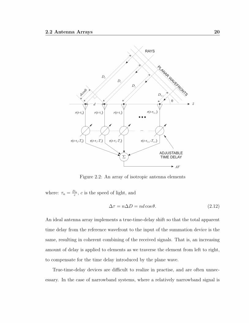
2.2 Antenna Arrays 20
Figure 2.2: An array of isotropic antenna elements
where: τn = Dn
c, c is the speed of light, and
∆τ = n∆D = nd cos θ. (2.12)
An ideal antenna array implements a true-time-delay shift so that the total apparent
time delay from the reference wavefront to the input of the summation device is the
same, resulting in coherent combining of the received signals. That is, an increasing
amount of delay is applied to elements as we traverse the element from left to right,
to compensate for the time delay introduced by the plane wave.
True-time-delay devices are difficult to realize in practise, and are often unnec-
essary. In the case of narrowband systems, where a relatively narrowband signal is

2.2 Antenna Arrays 21
modulated onto a radio carrier, time-delay devices can be approximated by phase
shifters as shown in Figure 2.3. Then if the distance from the nth antenna ele-
ment to a reference wavefront is Dn, we can express the phase delay or phase shift
accumulated along this distance as
ξn = k0Dn = k0(DN−1 + nd cos θ) (2.13)
where k0 is the propagation constant in free space,
k0 =2π
λ0
. (2.14)
Hence, a phase gradient is established along the axis of the array where the (n+1)th
element leads the phase of the nth element by k0d cos θ.
If the reference wavefront has a complex amplitude of 1, then the received signal at
the nth antenna element corresponds to ejξn . The amplitude/phase shifter modifies
the received signal such that at the output of the shifter, the signal is equal to
Inejξn , where In can be seen as a complex weight applied to the received signal.
The N signals at the output of the shifters are then combined to yield a composite
signal that goes to the receiver. With the normalized situation shown, this signal is
equivalent to the so-called array factor of the antenna array. It is equal to
AF = I0ejξ0 + I1e
jξ1 + I2ejξ2 + · · · + IN−1e
jξN−1 . (2.15)
If the reference element is element 0, the array factor can be expressed as
AF = I0 + I1ejk0d cos θ + I2e
j2k0d cos θ + · · · + IN−1ej(N−1)d cos θ (2.16)
=N−1∑
n=0
Inejk0nd cos θ. (2.17)
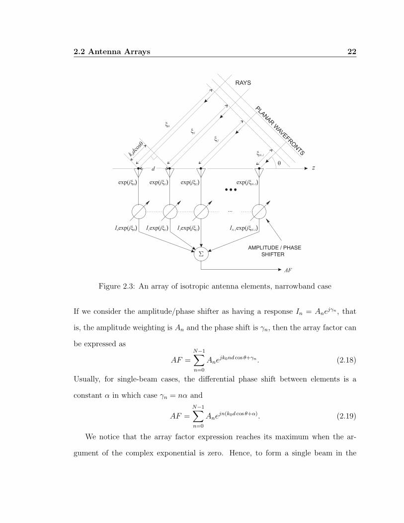
2.2 Antenna Arrays 22
Figure 2.3: An array of isotropic antenna elements, narrowband case
If we consider the amplitude/phase shifter as having a response In = Anejγn , that
is, the amplitude weighting is An and the phase shift is γn, then the array factor can
be expressed as
AF =N−1∑
n=0
Anejk0nd cos θ+γn . (2.18)
Usually, for single-beam cases, the differential phase shift between elements is a
constant α in which case γn = nα and
AF =N−1∑
n=0
Anejn(k0d cos θ+α). (2.19)
We notice that the array factor expression reaches its maximum when the ar-
gument of the complex exponential is zero. Hence, to form a single beam in the

2.2 Antenna Arrays 23
direction θ = θ0,
α = −k0d cos θ0. (2.20)
Examining Figure 2.3, we can see that by programming a phase gradient into the
phase shifters that counteracts (conjugates) the natural phase gradient established
by the incoming plane wave, all N signals entering the combiner are real-valued and
hence combined coherently to yield maximum signal strength at the receiver. It
can be easily seen that for any arbitrary phase distribution incident on the antenna
array, if the phase shifters can be programmed to conjugate the phase of the incoming
wave, the coherent combining condition will be maintained at the combiner. In a
transmission scenario, the phases must be conjugated to form the same beam as in
the reception scenario, due to reciprocity.
So far, arrays of perfectly isotropic elements have been considered. In practise,
antenna arrays are realized from non-isotropic elements with there own pattern factor
F (θ, φ), is discussed in Section 2.1. A well-known property of antenna arrays is that
the overall radiation pattern of the array is given by the product of the (isotropic)
array factor, and the pattern factor:
FTOTAL = Fe(θ, φ) · FA(θ, φ) (2.21)
where: FE is the pattern factor of the element used, and FA is the normalized array
factor of the antenna array.
2.2.2 Two-dimensional Planar Arrays
To achieve beam scanning in two principal planes instead of one, two-dimensional
planar antenna arrays are used. The basic operating principles are identical to that

2.2 Antenna Arrays 24
of one-dimensional arrays. Two-dimensional planar arrays are considered here since
planar arrays are used to realize reflectarrays, which are discussed in more detail in
Section 2.4.
A generic two-dimensional planar array is shown in Figure 2.4. Array elements
are arranged in a rectangular grid in the xy plane. There are M elements in the
x-direction and N elements in the y-direction, with corresponding element spacings
dx and dy, respectively.
Figure 2.4: Geometry of a two-dimensional planar array
The array factor of a 2-D planar array is calculated in a similar manner as for
a one-dimensional array. Since the array is arranged in a row-column format, it is
useful to address elements by row and column, and use a double-summation in the
array factor expression. If the complex weight applied to the element at index (m,n)

2.2 Antenna Arrays 25
is Imn = Amnejαmn , then the array factor of the planar array is denoted as
AF (θ, φ) =N−1∑
n=0
M−1∑
m=0
Amnej(k0r·r′
mn+αmn) (2.22)
=N−1∑
n=0
M−1∑
m=0
Amnejk0[x′mn sin θ cosφ+y′mn sin θ sinφ] (2.23)
where: r is the direction vector of the field point and r′mn = x′mnx + y′mny is
the position vector of the mnth element in the array. The dot product is readily
computed as
k0r · r′
mn= k0 [x′mn sin θ cosφ+ y′mn sin θ sinφ] . (2.24)
The pattern factor of the individual elements of the array can be multiplied by the
array factor to yield the total pattern from the array in two dimensions.
To phase the array to produce a beam in the direction (θ0, φ0), the phase shift of
element (m,n) is set so that
αmn = −k0 [x′mn sin θ0 cosφ0 + y′mn sin θ0 sinφ0] (2.25)
which is seen to perform the same phase conjugation effect as that described for a
one-dimensional array. Note that αmn is not a differential phase shift as in the case
of a one-dimensional array, but in this case represents an absolute phase value with
respect to a reference element.
2.2.3 Array Design Considerations and Directivity
Grating Lobes
Grating lobes are undesired beams in the antenna pattern that can produce beams as
strong as the main lobe in undesired directions. Major beams, including the desired

2.2 Antenna Arrays 26
beam, are formed whenever the argument to the complex exponential in the array
factor expression is zero, or in general, an integer multiple of 2π. In the case of a
one-dimensional array, whose array factor is given by equation (2.19), grating lobes
are formed whenever
k0d cos θ + α = 2kπ, k = 0, 1, 2, . . . (2.26)
If α = −k0d cos θ0, it is fairly simple to prove that to avoid grating lobes for all
possible scanning angles −90 ≤ θ0 ≤ 90,
d <λ0
2. (2.27)
For directional antenna elements in the array, which have a maximum response at
broadside (θ = 90), this condition can be relaxed somewhat since grating lobes
are naturally attenuated by the element factor of the constituent antennas due to
pattern multiplication.
Therefore, for beam-forming applications, antenna arrays are usually designed
with a period of a half-wavelength or less, unless there is natural rolloff in the pattern
introduced by the elements. This will be an important consideration in the design
of reflectarrays discussed in Chapter 4.
Amplitude Control of Elements
The discussion of beam-forming to this point has focused on manipulating the phase
of the antenna signals to manipulate the response of the beam. Manipulation of the
amplitude of the antenna signals, particularly through the use of amplitude tapers,
also affects the beam pattern. One- and two-dimensional amplitude tapers in one-
and two-dimensional planar antenna arrays have a strong effect on the sidelobe levels

2.2 Antenna Arrays 27
in the antenna pattern, and generally tapers are used for this function. They do not
affect the beam direction of the antenna. Introducing amplitude tapers is an effective
method to fine-tune the antenna pattern after the beam has been pointed. It is worth
noting that the price paid for reduced sidelobe levels possible with an amplitude taper
is a general reduction in directivity since it generally results in a broadening of the
main beam.
Additionally, specific beam shapes can be generated using array synthesis tech-
niques which demand a certain amplitude distribution across the surface of the array.
Like amplitude tapers, amplitude control in the array synthesis problems becomes
important when fine-tuning the beam shape, but does not affect the beam pointing
angle.
Though amplitude control adds flexibility to the configuration of the antenna
pattern, it will not be considered as a degree of freedom in the configuration of
the antenna pattern in this thesis. The reason for this is that reflectarrays, dis-
cussed later, do not generally support arbitrary amplitude distributions in the array.
Reflectarrays are usually constrained by the illumination pattern generated by the
feed antenna (as is the case for reflector antennas, discussed in Section 2.3), and
by the amplitude response of the reflectarray cells, which in this project was not
independently controllable from the phase response of the cells (this is discussed in
Chapter 3). However, knowledge of the effect of the antenna element signal ampli-
tudes must be taken into account when computing the overall gain of an antenna
array, regardless of whether the antenna signal amplitudes were under direct control
or not. The calculation of the gain produced by antenna arrays is considered in the
next section.

2.2 Antenna Arrays 28
Directivity
To compute the directivity of a two-dimensional planar array of isotropic elements,
we first consider the directivity of a one-dimensional array. We will assume that the
array is uniformly excited; that is, the amplitude of each and every antenna element
is the same (unity). This assumption is made for two reasons. First, it enables an
upper-bound on the array’s directivity to be computed. Since a reflectarray antenna
is subject to an amplitude taper from the feed horn, it will have a reduced direc-
tivity compared to the uniformly excited case. Second, reflectarray cell amplitude
effects cannot be analytically incorporated into a convenient directivity expression.
Therefore, the directivity expression requires numerical evaluation. The analysis pre-
sented here will allow for a rough estimation of a reflectarray’s directivity without
this computation.
To calculate the directivity of a one-dimensional array, first the beam solid angle
described by equation (2.7) is computed. Assuming the array elements are isotropic,
and that the peak of the array factor expression is reached in the visible region of
the array, the normalized array factor can be calculated as
F (θ) =sin(Nψ/2)
N sinψ/2(2.28)
which is just another representation of equation (2.19) with ψ = k0d cos θ+α. Then,
|F (θ)|2 =
∣
∣
∣
∣
sin(Nψ/2)
N sinψ/2
∣
∣
∣
∣
2
(2.29)
=1
N+
2
N2
N−1∑
m=0
(N −m) cosmψ. (2.30)

2.2 Antenna Arrays 29
The beam solid angle of equation (2.7) is then calculated as
ΩA =
∫ 2π
0
dφ
∫ π
0
|F (θ)|2 sin θdθ (2.31)
= 2π
∫ −k0d+α
k0d+α
|F (ψ)|2(
−1
k0d
)
dψ (2.32)
=2π
k0d
∫ k0d+α
−k0d+α
|F (ψ)|2dψ. (2.33)
Substituting 2.30 in the above equation and simplifying yields [2]
ΩA =4π
N+
4π
N2
N−1∑
m=1
N −m
mk0d2 cosmα sinmk0d. (2.34)
The directivity is then calculated as
D =
(
4π
N+
4π
N2
N−1∑
m=1
N −m
mk0d2 cosmα sinmk0d
)−1
. (2.35)
Equation (2.35) can be used to calculate the directivity of an array with arbitrary
uniform element spacing and inter-element phase shift. However, in Section 2.2.3,
the necessity to constrain the element spacing to half a wavelength for beam-forming
applications was discussed. Under this condition, k0d = π and the summation in
equation (2.35) is removed. The directivity simplifies to
D = N (2.36)
so that the directivity is simply equal to the number of elements used in the array1.
Hence, the gain scalability property of antenna arrays is clearly evident, in the ab-
sence of other loss effects. This result also provides a very easy way of computing
the peak directivity of a half-wavelength uniformly-excited one-dimensional antenna
1In fact, for small element spacings, directivity can exceed N and super-directivity can beachieved.

2.3 Reflector Antennas 30
array. Additionally, directivity is seen to be independent of scan angle for an array
with half-wavelength element spacing.
Identical arguments apply to a two-dimensional array with uniform excitation
and element spacings in both the x- and y- directions. Hence, the total number of
elements in a 2-D array can be used to predict an upper bound on its directivity,
which will become important when the directivity of reflectarrays is characterized in
Chapter 4.
2.3 Reflector Antennas
As the reflectarray is based on classical reflector antennas it is useful to study their
properties as well as the methods for calculating their radiation pattern and gain.
The analysis of reflectors is made quite interesting from the fact that many tech-
niques from optics are applied in determining the behaviour of these antennas. De-
tailed principles of reflector antennas can be found in [2] and the major points are
summarized here.
2.3.1 Principles of Operation
The most important property of a reflector antenna is its ability to collimate spherical
waves from a nearby feed horn into plane waves in the far field. An illustration of a
reflector was presented in Figure 1.2(a). For this illustration it is useful to examine
the properties of one of the most elementary reflector antennas, a parabolic reflector.
A parabolic reflector is shown in Figure 2.5 without the feeding antenna. A parabolic
reflector is named as such because its shape is described by a paraboloid of revolution.

2.3 Reflector Antennas 31
The equation describing the parabolic shape of the antenna is given by
(ρ′)2 = 4F (F − zf ), ρ′ ≤ a (2.37)
where: ρ′ is the displacement from the z-axis, ρ′ = a denotes the edge of the dish,
and (ρ′ = 0, zf = F ) is located at the apex of the dish. More conveniently, in polar
coordinates the shape of the reflector is described as
rf =2F
1 + cos θf(2.38)
where rf is the distance from the origin (feed point) to a point R on the reflector, as
shown in the figure.
Figure 2.5: Coordinate system for a parabolic reflector
A cross section of the reflector is shown in Figure 2.6. This figure illustrates
two fundamental features of a parabolic reflector that are the key to its collimating
action. These two features are as follows:
1. If a perfectly isotropic radiator is placed at the origin, the distance travelled by
a ray from the origin, to the reflector, to an imaginary aperture in the xy-plane

2.3 Reflector Antennas 32
Figure 2.6: Cross section of a parabolic reflector
is:
rf + rf cos θf =2F
1 + cos θf+
2F
1 + cos θfcos θf = 2F. (2.39)
For this reason, F denotes the so-called focal point of the reflector, since rays
emerging from this point all travel the same distance to the aperture plane.
2. Due to the law of reflection at the reflector surface, all rays emanating from the
focal point of the reflector are reflected so that the outgoing rays are parallel
to the z-axis. Geometrically, the surface normal n = NN
shown in the diagram
can be found by setting equation (2.38) to zero and taking the gradient of the
resulting equation. This results in
N = ∇
(
F − rf cos2 θf2
)
(2.40)
= rf cos2 θf2
+ θf cosθf2
sinθf2
(2.41)
which gives
n = −rf cosθf2
+ θf sinθf2
(2.42)

2.3 Reflector Antennas 33
and the fact that N2 = cos2 θf
2has been used in the normalization of N .
Computing the incident (αi) and reflected (αr) angles yields
cosαi = −rf · n = cosθf2
(2.43)
and
cosαr = z · n = (rf cos θf + θf sin θf ) · n (2.44)
= cos θf cosθf2
+ sin θf sinθf2
= cosθf2
(2.45)
which shows that the law of reflection is satisfied and the parabolic surface
indeed creates parallel rays from the incident ones.
Often, the reflector is stated in terms of its F/D ratio, where D is the subtended
diameter of the reflector as shown in Figure 2.6. The focal length and diameter of
the reflector used is determined by the characteristics of the feed antenna, which is
most commonly a horn antenna. The horn has limited beamwidth, and the horn is
chosen so that when the reflector is fed by a horn at the focal point, it is illuminated
efficiently. Usually, a 10 dB edge taper is chosen so that the reflector occupies the
10 dB beamwidth of the feed horn. The horn and reflector are usually designed
together to achieve an optimal F/D ratio for the application. Low F/D reflector
systems are smaller, but suffer from poorer cross-polarization characteristics, an issue
that reflectarrays potentially resolve as we will see in Section 2.4.
2.3.2 Radiation Pattern
To calculate the radiation pattern of a reflector antenna, the incident field is deter-
mined using characteristics of the feed antenna. Its amplitude (illumination taper)

2.3 Reflector Antennas 34
and phase characteristics are usually known. If the phase centre of the horn is known,
it is placed at the focal point to minimize phase errors from the reflector, and it can
be treated as a source of spherical waves over its beamwidth. Once the incident field
is known, it is projected onto the aperture plane. For reflector antennas, there are a
variety of approaches borrowed from geometrical optics or physical optics that can
be used to accomplish this, though those are not important for the discussion here.
Once the aperture distribution is known, it is used to compute the far field
radiation pattern of the antenna. This is facilitated through employing the surface
equivalence principle, whereby source fields within the antenna structure can be
simply replaced by equivalent electric and magnetic surface currents flowing on the
antenna itself. For aperture antennas such as reflector antennas, the equivalent
surface currents that need to be considered exist in the aperture plane like the xy-
plane shown in Figure 2.6; currents elsewhere are considered to be zero. Hence, by
projecting the incident field from the feed horn onto the aperture plane, the far field
pattern of the reflector (and its corresponding gain) can be determined.
The equivalent electric and magnetic surface currents are defined, respectively,
as
JS = n × Ha (2.46)
MS = Ea × n (2.47)
where Ea and Ha are the electric and magnetic fields in the aperture plane. From
these equivalent surface currents, magnetic and electric vector potentials can be
found using
A = µ0e−jk0r
4πr
∫∫
S
Js(r′)ejk0r·r′
dS ′ = µ0e−jk0r
4πrn ×
∫∫
S
Haejk0r·r′
dS ′ (2.48)

2.3 Reflector Antennas 35
and
F = εe−jk0r
4πr
∫∫
S
Ms(r′)ejk0r·r′
dS ′ = −εe−jk0r
4πrn ×
∫∫
S
Eaejk0r·r′
dS ′. (2.49)
where µ0 is the permeability of free space. We recognize the integrals as a 2-D
Fourier Transform, here relating variables in the spatial domain (equivalent electric
and magnetic surface currents) to quantities in angular space (A, F ). We can isolate
the Fourier transforms themselves and simplify the expressions by defining
P =
∫∫
S
Eaejk0r·r′
dS ′ (2.50)
Q =
∫∫
S
Haejk0r·r′
dS ′ (2.51)
and converting to spherical coordinates so that
A = µ0e−jk0r
4πr[θ cos θ(Qx sinφ−Qy cosφ) + φ(Qx cosφ+Qy sinφ)] (2.52)
F = −εe−jk0r
4πr[θ cos θ(Px sinφ− Py cosφ) + φ(Px cosφ+ Py sinφ)] (2.53)
where the radial (r) components have been dropped. Finally, the far-field electric
field can be calculated using the fact that
E = −jω(Aθθ + Aφφ) − jωη(Fφθ − Fθφ) (2.54)
where η is the intrinsic impedance of free space. The first term in the equation comes
from the standard definition of electric field when the magnetic vector potential is
known; the second term arises from the duality principle applied to the electric
vector potential. We see that essentially, the far-field electric field quantities are
simply sums of Fourier transforms of the component surface currents.

2.3 Reflector Antennas 36
The final components of the far-field electric field can be expressed as
Eθ = jk0e−jk0r
4πr[Px cosφ+ Py sinφ+ η cos θ(Qy cosφ−Qx sinφ)] (2.55)
Eφ = jk0e−jk0r
4πr[cos θ(Py cosφ− Px sinφ) − η(Qy sinφ+Qx cosφ)]. (2.56)
These expressions can be used to directly calculate the far-field radiation pattern of
a reflector antenna. Their importance will be become apparent when the far-field of
a reflectarray is considered mathematically in Chapter 4.
2.3.3 Directivity
To evaluate the directivity of a reflector antenna, or an aperture antenna in general
for that matter, we express the radiation intensity expression of equation (2.2) as
U(θ, φ) =1
2η[|Eθ|
2 + |Eφ|2]r2. (2.57)
Next, if we assume that the aperture fields are related as if they form a transverse
electromagnetic (TEM) wave, which is valid for electrically large apertures exceeding
a few wavelengths in extent, then
Ha =1
ηz × Ea. (2.58)
Substituting this in equations (2.55) and (2.56), and evaluating equation (2.57), we
find that
U(θ, φ) =k2
0
32π2η(1 + cos θ)2[|Px|
2 + |Py|2]. (2.59)
If we are to consider the maximum radiation intensity, so that we may determine
the maximum directivity of a reflector antenna, then we note that P attains its

2.3 Reflector Antennas 37
maximum value when the argument of the complex exponential in equation (2.50) is
completely real (i.e., we are pointed in the direction of the main beam), which yields
Um =k2
0
8π2η
∣
∣
∣
∣
∫∫
S
EadS′
∣
∣
∣
∣
2
. (2.60)
To evaluate the directivity of the reflector, we use equation (2.8). To compute the
radiated power from the aperture, we note that ideally the total power radiated from
the reflector is equal to the total power in the aperture. Assuming equation (2.58) is
valid, the power density in the aperture is S = |Ea|2/2η and the radiated power is
P =1
2η
∫∫
S
|Ea|2 dS ′ (2.61)
and the total directivity from the reflector antenna is
D =4π
λ20
∣
∣
∫∫
SEadS
′∣
∣
2
∫∫
S|Ea|
2 dS ′. (2.62)
If we try to calculate the upper limit of the directivity achievable from a reflector
antenna, then we should assume that the reflector is uniformly illuminated. This
is analogous to the assumption made in computing the maximum directivity of an
antenna array in Section 2.2.3, where the elements were assumed to be uniformly in
amplitude. If this assumption is made, then
∣
∣
∫∫
SEadS
′∣
∣
2
∫∫
S|Ea|
2 dS ′=A2p
Ap= Ap (2.63)
where Ap is the physical area of the aperture. Under this condition the directivity
expression reduces to a very powerful yet simple relationship given by
D =4π
λ20
Ap. (2.64)

2.3 Reflector Antennas 38
If we equate the maximum directivity of the reflector antenna to the directivity
expression given by equation (2.10), we quickly see that
Ae = Ap (2.65)
or the maximum effective area of the antenna is equal to its the area of its physical
aperture. This is a very important result for reflector antennas since it states that
the maximum gain of the reflector is ultimately limited only by the physical area of
the reflector used to realize the antenna.
2.3.4 Efficiency
Recall from equation (2.9) that the gain of an antenna is equal to its directivity
multiplied by an efficiency factor. Hence, the gain of a reflector antenna will only be
a fraction of equation (2.64). It is often expressed as
G = εapDreflector (2.66)
where εap is the so-called aperture efficiency of the antenna, which has a maxi-
mum value of unity. The aperture efficiency is actually the product of several sub-
efficiencies, each of which is separately accounted for as
εap = εrεtεsεa. (2.67)
Here, εr is the radiation efficiency which takes into account the ohmic losses of both
the feed and the reflector (these losses are generally very low). The remainder of the
terms are described in the following paragraphs.
The second term on the right-hand side of equation (2.67), εt, is known as the
taper efficiency of the reflector. An ideal aperture would have a uniform amplitude

2.3 Reflector Antennas 39
distribution over it surface, as mentioned numerous times previously. This efficiency
is the ratio of the actual power being received by the aperture relative to an ideal
aperture receiving a uniform power density over its surface. For example, for a
circular aperture,
εt =4F 2
πa2
∣
∣
∣
∫ 2π
0
∫ θ0
0Ff (θf , φ
′) tanθf
2dθfφ
′
∣
∣
∣
2
∣
∣
∣
∫ 2π
0
∫ θ0
0Ff (θf , φ′) sin θfdθfφ′
∣
∣
∣
2 (2.68)
where: Ff (θf , φ) is the feed pattern, and θ = θ0 denotes the edge of the reflector.
The third term on the right-hand side of the equation, εs, is the spillover efficiency
of the antenna. If the feed were perfect, it would not only illuminate the aperture
uniformly, but it would also not radiate past the edges of the aperture. A practical
feed possesses neither of these qualities. Although the feed power at the edge of the
reflector may be very low, it does not end abruptly. Feed energy that spills past the
reflector is not re-directed and is lost. Hence, we can express the spillover efficiency
of the antenna as∣
∣
∣
∫ 2π
0
∫ θ0
0Ff (θf , φ
′) sin θfdθfφ′
∣
∣
∣
2
∣
∣
∣
∫ 2π
0
∫ π
0Ff (θf , φ′) sin θfdθfφ′
∣
∣
∣
2 . (2.69)
Obviously, the taper efficiency and spillover efficiencies are in competition with
each other and a compromise must be struck between the two for practical feed
antennas. High taper efficiency, or a nearly uniform aperture, involves placing the
reflector such that it only occupies a small fraction of the feed horn’s beamwidth,
resulting in large spillover losses. Conversely, a system with low spillover losses
usually has a deep taper across the aperture. For practical feed antennas such as
horns, the product of taper and spillover efficiencies is usually maximum for a 10-
11 dB edge taper, which is why this value is often chosen.

2.4 Reflectarray Antennas 40
The final term in the aperture efficiency formula is the achievement efficiency,
which can be subdivided into the product of three sub-efficiencies. It is written as
εa = εφεcrεblk. (2.70)
The individual sub-efficiencies are:
• εφ, the phase error efficiency, which are phase errors in the aperture caused by
reflector deformities, surface errors, and feed phase error. All of these effects
can disturb the phase uniformity in the aperture and/or the reflection angles
of the reflector, reducing the gain of the antenna.
• εcr, the fraction of power that is maintained in the desired polarization of the
antenna. Some of the power is converted into a cross polarization component
by the feed antenna and/or the shape of the the reflector itself (especially if it
is offset fed).
• εblk, the aperture blockage efficiency, which results from shadowing of the re-
flector by the feed horn or other structure in front of the reflector.
Generally, most reflector antennas can achieve an overall aperture efficiency of
50% or better.
2.4 Reflectarray Antennas
Now that the concepts of both antenna arrays and reflectors have been discussed, the
reflectarray antenna can be addressed in detail. As discussed previously, reflectar-
rays blend concepts from both these antenna types, and the unique combination of
attributes from both has the potential to yield an attractive beam-forming platform.
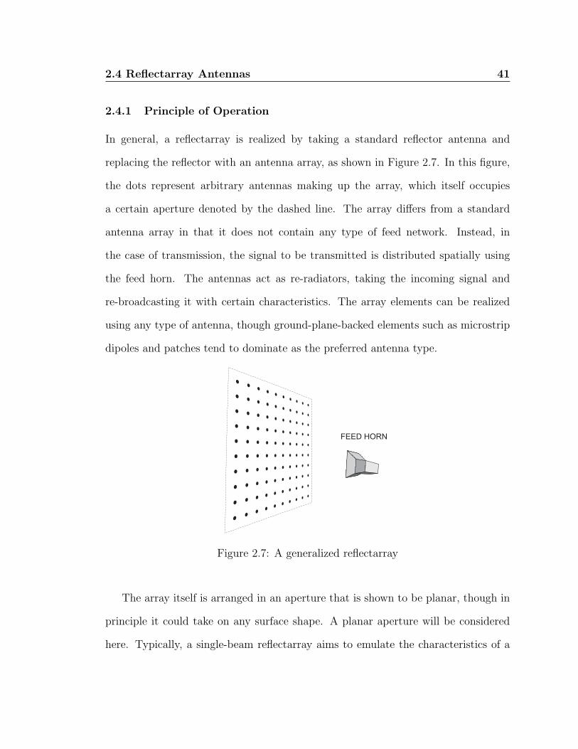
2.4 Reflectarray Antennas 41
2.4.1 Principle of Operation
In general, a reflectarray is realized by taking a standard reflector antenna and
replacing the reflector with an antenna array, as shown in Figure 2.7. In this figure,
the dots represent arbitrary antennas making up the array, which itself occupies
a certain aperture denoted by the dashed line. The array differs from a standard
antenna array in that it does not contain any type of feed network. Instead, in
the case of transmission, the signal to be transmitted is distributed spatially using
the feed horn. The antennas act as re-radiators, taking the incoming signal and
re-broadcasting it with certain characteristics. The array elements can be realized
using any type of antenna, though ground-plane-backed elements such as microstrip
dipoles and patches tend to dominate as the preferred antenna type.
Figure 2.7: A generalized reflectarray
The array itself is arranged in an aperture that is shown to be planar, though in
principle it could take on any surface shape. A planar aperture will be considered
here. Typically, a single-beam reflectarray aims to emulate the characteristics of a

2.4 Reflectarray Antennas 42
parabolic reflector as presented in Section 2.3. The geometry of a reflectarray is
shown in Figure 2.8. The geometry is similar to Figure 2.6 except that the reflected
ray is shown as leaving at an angle (θ0, φ0) from broadside (φ0 is not shown in the
figure), instead of being directed along the z-axis. The fact that the beam can be re-
directed at an arbitrary angle is one of the key features of the reflectarray, as opposed
to parabolic reflectors that have limited scanning capabilities. This results from the
fact that ideally, the antenna elements in the array can re-radiate the incident signal
with arbitrary phase. Hence, the principles of arrays explained in Section 2.2 can be
used to phase the array. The phases of the re-radiated signals are chosen such that
at an imaginary aperture plane in front of the reflectarray surface, electrically all the
radiated signals from the horn appear to have travelled the same distance. In the
case of a narrowband signal, this is approximately equivalent to having all signals
undergo the same phase shift.
Figure 2.8: Cross section of a reflectarray
Mathematically, this is expressed as follows. We first define a vector Ri = OR,

2.4 Reflectarray Antennas 43
and a vector RA having a unit vector ro, where the point R is the position of the
ith reflectarray element. For a perfectly phased situation, we have
k0(Ri − Ri · ro) − ψi = 2πn (2.71)
where i = 0, 1, 2, . . . N − 1, n is an integer, and N is the total number of elements
in the array. The term ψi represents the phase shift undergone by the ith element
between being received by the antenna element and being re-radiated. Hence, equa-
tion (2.71) represents a design equation stipulating the phase “surface” that must
be created to form a single beam in the direction (θ0, φ0).
The total far-field radiation pattern of a reflectarray is given by
ERA(θ, φ) =e−jk0r
r
N∑
i=0
Γi(θinci , φinci )Einc
i ejk0Ri ·ro (2.72)
where: Einci is the incident field received at the ith antenna element, and Γi is the
“re-radiation” or reflection coefficient of the ith element that takes into account both
losses inherent the element itself and scanning loss. This formula follows intuitively
from the array factor discussion in Section 2.2, where the element factor has been
absorbed into the reflection coefficient Γi. The angle of the reflection coefficient is
set so that 6 Γi = ψi as presented in equation (2.71).
Examining Figure 2.8, and comparing the operation of a reflectarray to a par-
abolic reflector, we make a few additional observations. First, the focal point of a
reflectarray is somewhat arbitrary. For a given desired beam angle, and a given feed
point in space, if the array is ideal it can be phased so that the beam is collimated
as desired. Practically then, the position of the feed is determined more by the illu-
mination characteristics of the feeding antenna and less by the location of its phase
centre, since this can be compensated for by the array.

2.4 Reflectarray Antennas 44
Second, if we are to compare the collimating action of a reflectarray to a parabolic
reflector, we notice some similarities and some differences. Recall that one of the
features of a parabolic reflector is that for an arbitrary ray, the total physical distance
from the focal point to the aperture plane was always 2F . In a reflectarray, this is
approximated by assuming the signal is narrowband, and establishing a condition
such that the total phase delay incurred from the feed to the aperture plane is
constant. Hence, we naturally expect the bandwidth of the reflectarray to be much
smaller than that achievable with a standard reflector antenna.
The other major difference in the reflective properties of a reflectarray is the
generation of so-called specular reflections, which is a potential source of loss in re-
flectarrays. Recall that for a parabolic reflector, the reflector is shaped such that
all rays from the feed are reflected parallel to the axis of the reflector. Examining
Figure 2.8, we see that this is not the case. For the ray shown, the angle of reflection
from the surface αr is equal to θf , leading partial reflection in a direction that is not
necessarily the desired direction θ0. Conversely, in a receiving mode, a plane wave
incident to the flat reflector may not be fully focused onto the feed horn because
of specular reflections off the reflector surface. Hence, in both cases, energy that is
not fully intercepted by the antenna elements and re-radiated will be lost. This has
practical implications on the design of reflectarrays and also impacts the design of re-
configurable antenna arrays. The ratio of specular reflection to the desired reflection
is an interesting theoretical problem and will be discussed more in Chapter 4.
With the basic principles of operation of reflectarrays presented, we now take the
opportunity to survey the state-of-the-art with regards to fixed reflectarray designs.

2.4 Reflectarray Antennas 45
2.4.2 Techniques for Realizing Fixed Reflectarrays
The concept of the reflectarray was first proposed in 1963 by Berry, Malech, and
Kennedy [5]. These researchers were the first to recognize some of the advantages
reflectarrays have over antenna arrays, namely, issues with loss in corporate feeding
networks in standard arrays. The authors succeeded in implementing the first ex-
perimental reflectarray using open-ended waveguides as the antenna elements. An
array of waveguides was fed by a feed horn, and the received signal coupled into the
section of waveguide at each antenna element. The other end of the waveguide was
short-circuited, leading to a reflection of the received signal and re-radiation out the
end of the open side of the waveguide. By controlling the lengths of the individual
waveguide elements, the phase of the re-radiated signal could be manipulated and
hence, the array phased to form the desired beam.
Interest in reflectarrays did not re-emerge until the late 1980’s, when a patent
was issued describing the first planar implementation of a reflectarray [6]. Microstrip
patch antennas were proposed as the antenna elements of choice. By loading the
patch antennas with open-circuited microstrip stubs, the appropriate phase shift
could be introduced between the received signal and re-radiated signal by simply
varying the length of the stub. Assuming the stub circuit is electrically matched
to the patch antenna, the entire signal received by the patch antenna enters the
stub circuit, is reflected by the open circuit (which has a reflection coefficient of 1),
and re-enters the patch where it is radiated with the accumulated phase shift from
the stub circuit. Designing the reflectarray consists of placing the feed horn at an
appropriate distance and choosing the stub lengths appropriately to collimate the

2.4 Reflectarray Antennas 46
feed signal in the desired direction. In the patent, the reflectarray was proposed as a
technique for enhancing or reducing the radar cross section (RCS) of an object. By
forming a reflectarray on the surface of an object, incident waves could be directed
back in the direction of the transmitter (enhancing RCS) or directed in a different
direction (reducing RCS).
In 1991, Huang [4] recognized that reflectarrays have an enormous potential for
use in space communications, because of their low profile and low weight. Since they
can conform to surfaces, the bulk and weight of a traditional parabolic reflector can be
eliminated. Huang was the first to conduct an experimental study on the feasibility
of using microstrip reflectarrays and study the amount of backscatter generated from
specular and diffraction fields. The major conclusion was that large arrays would not
suffer from serious backscatter effects, and that the efficiency of reflectarrays would
increase as they become larger.
Ideas presented by Munson and Huang sparked a prolific interest in reflectarrays
that has lasted until the present day. Most of the research on reflectarrays involved
analysis and development of reflectarray cells with desirable scattering character-
istics. As such, the methods for manipulating the phase response of cells became
aggregated into three rough groups, where the scattering response of cells is manip-
ulated by:
• loading the reflectarray elements with stubs, as already discussed;
• changing the shape and/or size of reflectarray elements;
• pursuing circularly-polarized cells where the scattering response can be modi-
fied by changing the orientation of antenna elements.

2.4 Reflectarray Antennas 47
These techniques are explained in greater detail next.
Reflectarrays Based on Stubs
Reflectarray elements based on tuning stubs received a lot of attention in the infancy
of reflectarrays due to their straightforward nature and the fact that the scattered
field phase range was not constrained. Stubs do not appreciably affect the radiation
pattern of the antenna when they are less than a half-wavelength in extent [7].
Usually, the stubs must be bent orthogonally to accommodate them in large arrays.
The first experimental realization of a microstrip reflectarray based on stubs was
presented by Chang et al [8]. The prototype operated at 12 GHz and consisted
of 2828 linearly polarized elements. It provided a gain of 32.5 dBi. The authors
also identified that reflectarrays based on stubs suffered from poor cross-polarization
characteristics, because of radiation contributions from the orthogonally bent stubs.
To improve the cross-polarization performance of the reflectarray, the authors later
introduced symmetry in the way the stubs were laid out the reflectarray so that
cross-polarization components would cancel [9]. They also introduced the concept of
a dual-polarization, dual-feed reflectarray in this work by introducing tuning stubs
in both the E-plane and H-plane of the patch antenna.
A more rigorous analysis of the radiation pattern produced from stub-based re-
flectarrays was presented in [10], based on a method of moments (MoM) analysis. A
detailed analysis of the stub-loaded microstrip reflectarray elements themselves was
presented in [11]. As the body of knowledge of reflectarray continued to expand,
an increasing amount of research effort was being put into examining alternative
phase-shifting techniques. By the late 1990’s, much of the research effort had shifted
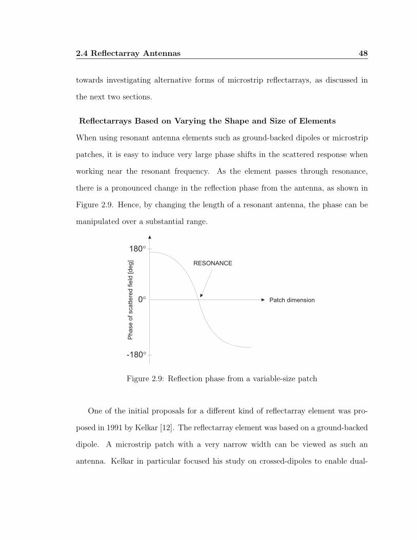
2.4 Reflectarray Antennas 48
towards investigating alternative forms of microstrip reflectarrays, as discussed in
the next two sections.
Reflectarrays Based on Varying the Shape and Size of Elements
When using resonant antenna elements such as ground-backed dipoles or microstrip
patches, it is easy to induce very large phase shifts in the scattered response when
working near the resonant frequency. As the element passes through resonance,
there is a pronounced change in the reflection phase from the antenna, as shown in
Figure 2.9. Hence, by changing the length of a resonant antenna, the phase can be
manipulated over a substantial range.
Figure 2.9: Reflection phase from a variable-size patch
One of the initial proposals for a different kind of reflectarray element was pro-
posed in 1991 by Kelkar [12]. The reflectarray element was based on a ground-backed
dipole. A microstrip patch with a very narrow width can be viewed as such an
antenna. Kelkar in particular focused his study on crossed-dipoles to enable dual-

2.4 Reflectarray Antennas 49
polarization usage in reflectarrays. The major outcome of this work was to illustrate
that by manipulating the length of the dipole over 0.25 − 0.60 wavelengths, close to
a 360 phase shift in the scattered field could be achieved. An experimental reflec-
tarray based on this concept, named FLAPS (FLat Parabolic Surface) was built and
demonstrated.
The use of microstrip dipoles or crossed dipoles as reflectarray elements would
not persist for long. Researchers recognized that they suffered from very narrow
bandwidths, and furthermore were more prone to ohmic losses due to their thin
metallic nature. Hence, there was a shift to using variable-length microstrip patches
for the same purpose. Crossed-dipoles did attract some attention years later for
applications where it is desirable to have small antenna footprint, as in the case of
reflectarrays integrated with solar panels [13].
The first reflectarray based on variable-sized patches was presented in [14]. The
reflectarray in this work was shown to provide equivalent performance to an identical
reflectarray based on tuning stubs. The experimental design provided 27 dBi of gain,
and also exhibited superior cross-polarization performance compared to the stub-
based design, which is expected. This work ultimately led to one of the the seminal
papers on reflectarray design [15], which presented design and analysis techniques for
both the array and the elements themselves, using a MoM approach. The techniques
allowed for successful designs of numerous reflectarrays at 28 GHz and 77 GHz, based
on both prime-focus and cassegrain feeds.
Research has also provided insight into the effect of patch parameters on scat-
tering performance. The effect of substrate permittivity [16] and substrate thick-
ness [17] was investigated, as well as a study of the limits of phase range provided

2.4 Reflectarray Antennas 50
by this approach [18].
A number of interesting implementations of reflectarrays based on variable-sized
patch elements have been proposed. Recently, Pozar [19] described the design and
construction of a specialized reflectarray for producing shaped-beam patterns. This
contrasts significantly with reflectarrays designed to produce pencil-beam patterns,
for which the design equation of (2.71) can be used. Shaped-beam reflectors are
used in satellite applications to produce very specific continental illumination pat-
terns, and require special synthesis techniques to provide the desired pattern. More
recently, a novel feed configuration for a variable-patch-based reflectarray has been
proposed [20], whereby a line source such as a dipole is used to feed the array. Ap-
proaches based on fixed patch sizes and a variable-length slots in the ground plane
behind the patch have also been demonstrated to achieve the same phase shifting
effect [21].
One of the biggest disadvantages of a variable-length patch compared to a stub-
loaded patch is that the realizable phase range in the scattered field is quite limited.
It is a function of substrate height, substrate permittivity, patch dimensions, and is
usually selected so that other important parameters such as the slope of the phase
characteristic and bandwidth are not compromised [22]. However, usually the phase
range attainable using this technique is much less than 360. Therefore, unlike the
stub-loaded patch, there is always an unattainable phase range that leads to phase
errors in the reflector surface. This approach may also lead to increased specular
reflection from the array because of the large differences in radar cross section of the
constituent elements.
Recognizing this deficiency, a number of researchers started looking into stacked-
2.4 Reflectarray Antennas 51
patch topologies. In 2001, Encinar [23] demonstrated a stacked patch structure
consisting of two different-sized patches stacked over top of each other. This yielded
a smoother phase-versus-size characteristic, and more importantly, yielded phase
ranges far in excess of 360. In particular, by varying the dimensions of only one of
the two stacked patches, over 600 of phase range was demonstrated in a 12 GHz
design. The design also provided a substantial improvement in reflectarray oper-
ating bandwidth, extending its bandwidth from what is typically a few percent to
over 16%. An experimental prototype providing 31 dBi of gain at 12 GHz was
demonstrated, and was later adapted into a shaped-beam reflector for continental
illumination [24]. A numerical technique for analyzing stacked-patch reflectarray el-
ements was presented by some of Encinar’s collaborators one year later [25], as well
as a stacked-patch reflectarray prototype [26].
It is difficult to achieve large operating bandwidths for large reflectarrays be-
cause of the large spatial delay between the feed and the outermost antenna el-
ements, which requires phase compensation exceeding 360 to provide broadband
operation. Broadband operation can be achieved using such devices because es-
sentially the phase shifter is more closely approximating a true-time-delay device.
To further broaden the bandwidth, a three-layer printed reflectarray was proposed
in [27] whereby an optimization technique is used to provide suitable array phasing
over a substantial frequency range. The three-layer structure was later applied to
applications in contoured beam space applications [28] and local multipoint commu-
nications systems [29]. The issues of bandwidth and scanning loss associated with
large reflectarrays have also been addressed by assembling reflectarray panels in a
shape approximating a shaped reflector [30].

2.4 Reflectarray Antennas 52
The variable-size patch approach described thus far has been used for reflectar-
rays utilizing one or two independent, linear polarizations. The length and/or width
of the patch are varied in order to change the reflection phase of one incident polar-
ization. A unique implementation of the variable-size patch technique has recently
been employed for folded reflectarrays [31]. The feeding of folded reflectarrays re-
sembles that of a cassegrain-fed reflector, where the feed aperture is located in the
reflector itself and a sub-reflector in front of the reflector is used to distribute the
feed signal. In the case of a folded reflectarray, the sub-reflector is replaced by a
polarizing grid which is cross-polarized relative to the feed polarization so all the
feed energy is reflected back towards the reflectarray. The patches in the reflectarray
surfaces are rotated 45 with respect to the incident field, and the width and length
of the patch are designed to rotate the incoming signal’s polarization by 90 while
simultaneously applying the desired phase shift to the outgoing polarization. Hav-
ing its polarization twisted by 90, the outgoing signal from the reflectarray surface
passes uninhibited through the polarizing grid.
Here, the use of variable-sized patches is quite different from other approaches
in that the width and length of the patch must be both manipulated independently
to achieve two things: the twisting of the polarization and the application of a
phase shift to the re-radiated wave. Since the patch is oriented 45 relative to the
incident polarization, it will produce reflected radiation consisting of two polarization
components. The patch width and length are chosen to give a 180 relative phase
shift between these components to achieve the polarization twist. Since a large
number of width/length combinations give this result, the designer is free to choose
a combination yielding the appropriate reflection phase shift to give the desired
2.4 Reflectarray Antennas 53
phasing action of the array as a whole. This approach has been used to realized
a number of reflectarrays for communications [32] and RADAR applications [33].
Most recently, the ability to modify the amplitude of the feed distribution has been
demonstrated by integrating an additional reflectarray with the polarizing grid [34].
It is worth noting that manipulating the shape of other types of patch elements
has also been proposed in the literature. Historically, collimating spherical waves us-
ing a planar surface was first contemplated in the design of Fresnel zone reflectors [35],
which later evolved into using variable-sized, non-uniformly spaced microstrip discs
to achieve the same effect [36]. Other microstrip patch elements with unique shapes
have also been employed to try to improve the overall trade-off between phase range,
phase slope, and bandwidth typically faced by reflectarray designers [22].
To this point, we have covered stub-loaded patches and variable-sized patch el-
ements as reflectarray elements. Both of the approaches discussed so far are for
linearly-polarized reflectors. There is also a whole class of reflectarray elements de-
signed for circularly-polarized systems, as discussed in the next section.
Circularly-Polarized Reflectarray Elements
Microstrip patch antennas are capable of receiving circular-polarized (CP) signals
since these signals can be decomposed into two orthogonal polarizations correspond-
ing to the two radiation axes of a patch antenna. It has been known for some time
that a simple way to apply a phase shift to an incoming CP wave is to physically
rotate the patch. The phase delay corresponds to the physical rotation of the patch;
that is, if the patch was rotated ψ, the phase shift applied to the received signal is
also ψ.
2.4 Reflectarray Antennas 54
This fact was exploited to realize the first CP reflectarrays, which were first
proposed in [37] and later expanded upon in [38]. In this implementation, tuning
stubs are used along both axes of the patch to induce a 90 phase shift between
polarizations so that the reflected CP wave has the same polarization (handed-ness)
as the incident wave. Then, by physically rotating the element, a phase shift can
be achieved similar to CP-phased arrays described earlier based on rotating the
elements, the difference being that the phase shift applied to the reflected signal
is doubled because of the reflection process. Phase shifting can also be achieved
without element rotation by adjusting the stub lengths, provided that a 90 phase
shift between polarizations is maintained, but it was shown by the researchers that
the variable-angle approach produced superior performance in terms of sidelobe and
cross-polarization levels [38]. The authors were able to achieve 42 dBi of gain in
the Ka-band using a 6924-element reflectarray. Work continues on this fascinating
concept, and the variable-rotation patch approach has recently been used to realize
inflatable reflectarrays for space applications employing over 200,000 elements in a
3 metre reflector [39].
Other CP elements have also been investigated. A range of elements, includ-
ing dipoles, slots, and shorted discs was investigated in [40]. Researchers have also
looked at slot rings [41] and microstrip ring elements for CP reflectarrays [42], which
use the same principle of physical rotation to achieve reflection phase shift. Ring
elements are more compact than microstrip patches and possess a unique quality
that they are transparent at non-resonant frequencies. The latter quality has been
exploited to realize dual-frequency reflectarrays by stacking two reflectarrays at dif-
ferent frequencies [43], making them highly attractive for satellite applications which

2.4 Reflectarray Antennas 55
use separate uplink and downlink frequencies for communication. This technology
has been demonstrated on inflatable, thin-membrane dual-frequency reflectarrays for
space applications [44]. Their transparent nature also allows them to be stacked to
improve bandwidth [45] as with standard patch-based reflectarray cells.
2.4.3 Tunable Reflectarrays
The plethora of techniques for manipulating the phase response of reflectarray ele-
ments is now quite apparent. Section 2.4.2 has presented a large number of design
techniques for fixed reflectarrays employing linear polarization, circular polarization,
and dual-polarizations. However, all the techniques presented focused on designing
a reflectarray with a static radiation pattern. Once the reflectarray itself is designed
it is realized by photolithographic techniques. In essence, the reflectarray pattern is
permanently “printed” on a substrate with no possibility of changing it afterwards
without re-designing it.
This section presents an overview of techniques that have been suggested to make
reflectarray radiation patterns adjustable. The concept has indeed been proposed,
but as we will see, there has been very little demonstrated experimentally in this
field for a variety of technical and practical reasons.
The idea of a tunable reflectarray is certainly not new. Indeed, it was contem-
plated at the very time the reflectarray concept was first proposed. In the first pub-
lished paper on reflectarrays [5], the authors identified the potential of reflectarrays as
dynamic beam-forming platforms and proposed that by introducing diode-switched
short circuits along the length of the waveguide, the phase response of each element
could be changed. This concept was never experimentally realized due to limitations

2.4 Reflectarray Antennas 56
of technology at the time. The idea of tunability was also presented in the reflec-
tarray patent by Munson [6], where the authors proposed that by introducing phase
shifters in the stub circuit, dynamic beam forming could be possible.
Javor et al [46] proposed placing switches, or even phase-shifting devices, in the
stub circuit to achieve beam-steering capability, though physical tuning devices were
never experimentally demonstrated with the reflectarray. Tunability has also been
suggested for microstrip-dipole based reflectarrays. It was conceptually proposed by
Cooley, who demonstrated through electromagnetic simulations that the rotation of
a dielectric rod placed directly beneath the microstrip dipole element could effect a
significant phase shift in the re-radiated signal [47]. However, none of these efforts
resulted in any experimental devices.
Circularly-polarized cells also are, at least conceptually, very amenable to dy-
namic phase adjustment. Huang proposed that the CP elements described in [38]
could be mounted in miniature motors to enable the physical rotation (and hence
electrical phase shift) of the elements to be manipulated. This technique has a sig-
nificant advantage in that an entire 360 of tuning range could be achieved by simply
rotating the element by 180.
The phase response of CP elements can also be manipulated by the use of RF
switches. This idea was first proposed by Malagasi in 1978 [48], who described
microstrip disc elements with electronically controlled switches connected to shorting
pins that when actuated, electronically rotated the disc element. Many years later,
the same concept was applied to dipoles whereby a number of dipoles of varying
angles were overlaid on top of each other, and an RF switch uses to short the two
arms of the “active” dipole and hence select the desired rotation angle [49]. Micro-

2.4 Reflectarray Antennas 57
electro-mechanical systems (MEMS) switches were also proposed for this application
though never physically realized [50].
MEMS switches were also proposed in an alternative reflectarray topology based
on flared notch antennas [51]. A planar horn-type antenna was proposed whereby a
series of MEMS switches are placed along the throat of the notch. By switching on
MEMS switches, the electrical distance traversed by a received signal inside the flared
notch could be changed, resulting in a true-time-delay type of array. Unfortunately,
though MEMS switches were realized, they were never experimentally integrated
with the horn and instead the characteristics of the reflectarray were demonstrated
by embedding switch measurements in simulations.
Yet another approach amenable to MEMS technology was proposed in [52],
whereby the height of a patch antenna over the ground plane is varied to achieve the
phase-shifting action. Though experimental results with fixed patches demonstrated
beam-forming, the approach suffered from a limited phase tuning range. Further-
more, MEMS devices with appropriate mechanisms for adjusting the patch height
have not been demonstrated.
The most promising approach to date has been based on active tuning devices
such as varactor diodes. One such approach was demonstrated in a small reflectarray
in [53]. In this topology, the radiating edge of a patch antenna was loaded with a
varactor diode in order to change its electrical length and subsequent re-radiated field.
Unfortunately only a 180 phase range was achieved with this element, allowing for
only limited beam scanning and constraining its application to small reflectarrays.
This problem was recently alleviated using an active cell topology [54] though an
array based on this cell has not yet been demonstrated.

2.4 Reflectarray Antennas 58
An interesting and recent development has been the development of tunable im-
pedance surfaces [55], which are capable of being adapted for used as reconfigurable
reflectors [56]. However, only a bulk phase gradient can be programmed into such
structures, allowing for limited beam-forming functionality, especially if the full flex-
ibility of an antenna array is desired. Additionally, because only phase gradients can
be programmed into the surface, it cannot be used as a spherical-to-plane wave con-
verter and hence cannot be easily integrated with a feeding antenna as a stand-alone
antenna.
From the foregoing discussion, it appears that there have been only limited at-
tempts at making electronically tunable reflectarrays. There have been a large num-
ber of conceptual proposals, based on both mechanically-tuned and electrically-tuned
antennas, but very little demonstrated in terms of operating hardware. To the best
of the author’s knowledge, there has not been a successful implementation of an
electronically tunable reflectarray cell possessing the necessary agility to realize a
reconfigurable antenna with a large degree of adaptability. It was this need that
catalysed the motivation to develop a phase agile reflectarray cell, the design of
which is the topic of discussion of the next chapter.

Chapter 3
A Phase-Agile Reflectarray Element
Concepts for manipulating the scattered phase of fixed reflectarray elements
were presented in Chapter 2. A number of ideas reported in the literature for
adding tunability to reflectarray elements were also discussed. This chapter presents
a proposal for an electronically tunable reflectarray cell that achieves a large degree
of phase agility. Details on the design of the reflectarray cell are given, as well
as a presentation of several techniques that can be used to predict the scattering
characteristics of the element. Experimental characterization techniques and results
are also provided at the end of the chapter.
3.1 Proposed Element Design
For many linearly-polarized reflectarray cells, the fundamental mechanism which
provides changes in the phase of the scattered field from the cell is a change in the
resonant frequency of the microstrip patch element. This is usually implemented
by adjusting the shape or loading of the patch element in fixed reflectarrays. The
proposed reflectarray cell utilizes concepts developed for frequency agile antennas,
where the resonant frequency of a patch is modified electronically using varactor
diodes [57][58]. A similar concept has also been used to reduce scan blindness in
regular microstrip antenna arrays [59]. The basic idea is that by loading the mi-
crostrip patch with an electronically-controllable capacitance, its resonant frequency

3.1 Proposed Element Design 60
can be changed to increase the usable frequency range of the patch. The resulting
frequency agility, when applied to arrays of microstrip patches, can be used to change
the scanning characteristics of the array.
As mentioned in Section 2.4.3, some researchers attempted using a similar con-
cept to implement a tunable reflectarray element. Unfortunately, only a limited
phase range was achieved using their structure. Hypothetically though, by carefully
choosing the size of the patch and the location of the varactor diodes, it should be
possible to get much more phase range from the structure. This is the hypothesis
of the present research: matching the characteristics of the patch and diode should
allow the phase agility of the patch to be maximized.
To do this, it is important to consider both the size of the patch and the range of
capacitances produced by the varactor tuning diode. The element must be designed
so that for a patch with a given size, the maximum change in resonant frequency
is produced over the range of capacitances offered by the varactor diode. This di-
rectly translates into scattered field phase range. As an example, consider a patch
employing shunt-connected varactor diodes along its radiating edges, as shown in
Figure 3.1. As the patch naturally establishes a fringing capacitance Cf along the
patch edges, the shunt varactor diode adds to the total capacitance seen at the patch
edges. The resonant frequency of the patch is determined by its length L (and to
some degree width, W ), and by the total edge capacitance. Manipulating the ca-
pacitance seen at the edge of the patch is the basis of frequency agile antennas. The
resonant frequency of the patch can be reduced by increasing the edge capacitance,
up to a point.
To produce as large a change in the patch’s resonant frequency as possible, the

3.1 Proposed Element Design 61
TOP VIEW
SIDE VIEW CfCf
W
L
Figure 3.1: Frequency agile antenna based on a shunt tuning diode
varactor diode must possess a capacitance of the same order of magnitude as the
fringing capacitance. A diode with too large a capacitance will cause the diode to
dominate the total capacitance produced at the edge of the patch, producing limited
frequency (and phase) agility. Hence, the diode’s capacitance must be selected on
the basis of the patch’s size, or vice versa.
To understand this concept further, consider the plots shown in Figure 3.2. The
upper plot illustrates the scattered field phase from a frequency-agile patch antenna
as a function of frequency. A varactor diode is used which has a fixed tuning range
of Cmin to Cmax. As the capacitance is increased in uniform steps, the resonant
frequency of the patch is reduced, though the reduction diminishes with increasing
frequency. The operating frequency (or likewise, the patch size) must be selected
carefully to maximize the phase agility of the element. Taking various slices through
the upper plot at different operating frequencies (or patch sizes) produces the plots
shown in the lower plot, which shows the scattered field phase as a function of tuning
capacitance C.
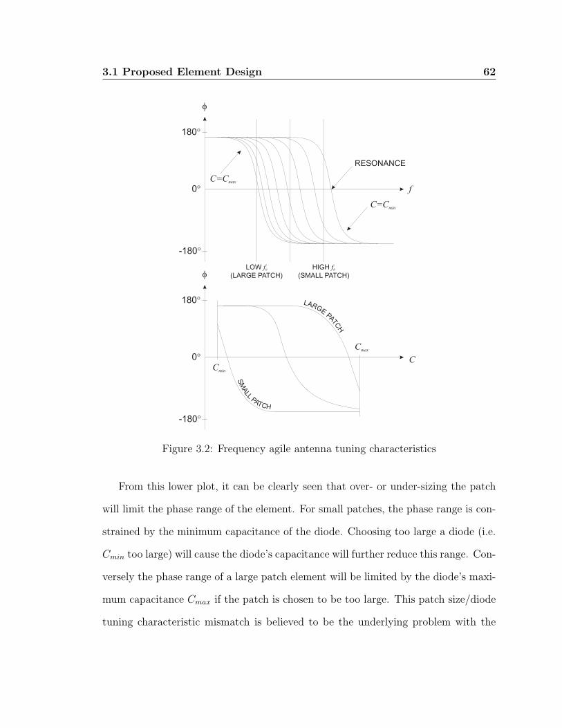
3.1 Proposed Element Design 62
Figure 3.2: Frequency agile antenna tuning characteristics
From this lower plot, it can be clearly seen that over- or under-sizing the patch
will limit the phase range of the element. For small patches, the phase range is con-
strained by the minimum capacitance of the diode. Choosing too large a diode (i.e.
Cmin too large) will cause the diode’s capacitance will further reduce this range. Con-
versely the phase range of a large patch element will be limited by the diode’s maxi-
mum capacitance Cmax if the patch is chosen to be too large. This patch size/diode
tuning characteristic mismatch is believed to be the underlying problem with the
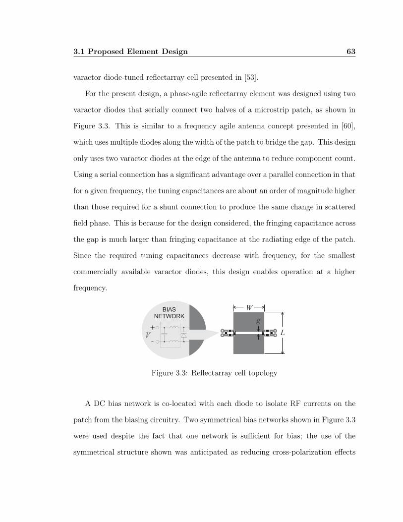
3.1 Proposed Element Design 63
varactor diode-tuned reflectarray cell presented in [53].
For the present design, a phase-agile reflectarray element was designed using two
varactor diodes that serially connect two halves of a microstrip patch, as shown in
Figure 3.3. This is similar to a frequency agile antenna concept presented in [60],
which uses multiple diodes along the width of the patch to bridge the gap. This design
only uses two varactor diodes at the edge of the antenna to reduce component count.
Using a serial connection has a significant advantage over a parallel connection in that
for a given frequency, the tuning capacitances are about an order of magnitude higher
than those required for a shunt connection to produce the same change in scattered
field phase. This is because for the design considered, the fringing capacitance across
the gap is much larger than fringing capacitance at the radiating edge of the patch.
Since the required tuning capacitances decrease with frequency, for the smallest
commercially available varactor diodes, this design enables operation at a higher
frequency.
Figure 3.3: Reflectarray cell topology
A DC bias network is co-located with each diode to isolate RF currents on the
patch from the biasing circuitry. Two symmetrical bias networks shown in Figure 3.3
were used despite the fact that one network is sufficient for bias; the use of the
symmetrical structure shown was anticipated as reducing cross-polarization effects

3.2 Unit Cell Modelling 64
and was based on the discussions of symmetrical reflectarray designs discussed in [9].
The optimal pairing of the diode to the patch structure is facilitated through the
use of electromagnetic simulations and an equivalent circuit model, both of which
will now be discussed.
3.2 Unit Cell Modelling
Modelling of the unit cell is performed by making two assumptions. First, it is
assumed that the cell is embedded in an infinite array, surrounded by identical cells
in the transverse plane. For large reflectarrays, this is a good assumption as edge
effects are not significant, especially when the edge taper of the feed is included.
Second, it is assumed that the patch is illuminated at broadside. While not all
elements will be receiving signals at this angle, it has been shown that the scattered
field broadside to the cell closely approximates the scattered field of a microstrip
within about 40 of broadside [14]. Hence, broadside illumination will be used in the
analysis.
The analysis scenario is illustrated in Figure 3.4. The scattering behaviour can be
analyzed by computing the reflection coefficient of a unit cell of dimensions d×d in an
infinite array, as shown in Figure 3.4. An incident plane wave with electric field Einc
is launched toward the patch and the TEM reflection coefficient Γ computed from
the scattered field. This reflection coefficient can be used to predict the amplitude
and phase of the scattered signal.
The patch structure itself is assumed to have a length L and width W . It is
printed on a substrate with a dielectric constant of εr and height h. We now con-
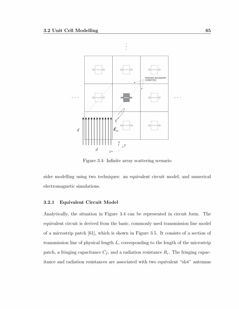
3.2 Unit Cell Modelling 65
Figure 3.4: Infinite array scattering scenario
sider modelling using two techniques: an equivalent circuit model, and numerical
electromagnetic simulations.
3.2.1 Equivalent Circuit Model
Analytically, the situation in Figure 3.4 can be represented in circuit form. The
equivalent circuit is derived from the basic, commonly used transmission line model
of a microstrip patch [61], which is shown in Figure 3.5. It consists of a section of
transmission line of physical length L, corresponding to the length of the microstrip
patch, a fringing capacitance Cf , and a radiation resistance Rr. The fringing capac-
itance and radiation resistances are associated with two equivalent “slot” antennas

3.2 Unit Cell Modelling 66
formed at the edge of the patch. The parameters of the transmission line, such as its
characteristic impedance Zc and phase constant βeff are computed using standard
formulae for microstrip transmission line.
Zc, βeffCf RrCfRr
W
L
L
εr h
Γ
Figure 3.5: Equivalent circuit for predicting scatter from an unmodified microstrippatch
No probe feed is shown in Figure 3.5, unlike the standard transmission line model,
because the patch is not being fed. Instead, the patch is excited through its two
slot radiation resistances Rr with anti-symmetric voltage sources. This models the
excitation established when the patch scatters energy from a plane wave incident
broadside to the patch. The two voltage sources correspond to the electric fields
produced in the two slots formed at the ends of the microstrip patch. Computing

3.2 Unit Cell Modelling 67
the reflection coefficient as seen from one of the sources (with Rr acting as the source
resistance), amounts to computing the reflection coefficient shown in Figure 3.4. That
is, the reflection coefficient seen looking in to the source is reflection coefficient of
a unit cell embedded in an infinite array scenario. The amplitude and phase of the
reflection coefficient correspond to the amplitude and phase of the scattered wave
from the unit cell.
Obviously, the patch shown in Figure 3.5 is not the same as the structure shown
in Figure 3.3. The circuit model can be appropriately modified, whereby models
for discontinuities are inserted at the point indicated by the arrow in Figure 3.5.
The adaptations to the basic circuit model and discontinuities are described in more
detail in the following paragraphs.
First, the patch is partitioned into two halves of length L/2− g/2, where g is the
gap width indicated in Figure 3.3. The gap discontinuity can be represented using a
π equivalent circuit [62] as shown in Figure 3.6. A series capacitance Cs represents
the fringing capacitance between the two patch halves, while two shunt capacitances
Cp model the capacitance between the patch ends and the ground plane, similar to
Cf .
Next, for the moment we assume that two short circuits are placed across the gap
at positions corresponding to that of the varactor diodes, as shown in Figure 3.7.
We do this because we know that the varactor diodes will conduct the bulk of the
RF current if the structure is close to resonance. Hence, currents that were pre-
viously flowing unconstrained across the patch surface now are constrained to flow
around the slot in the patch. This leads to current crowding, which can be modelled
approximately using an inductance Lc, as shown in the figure.
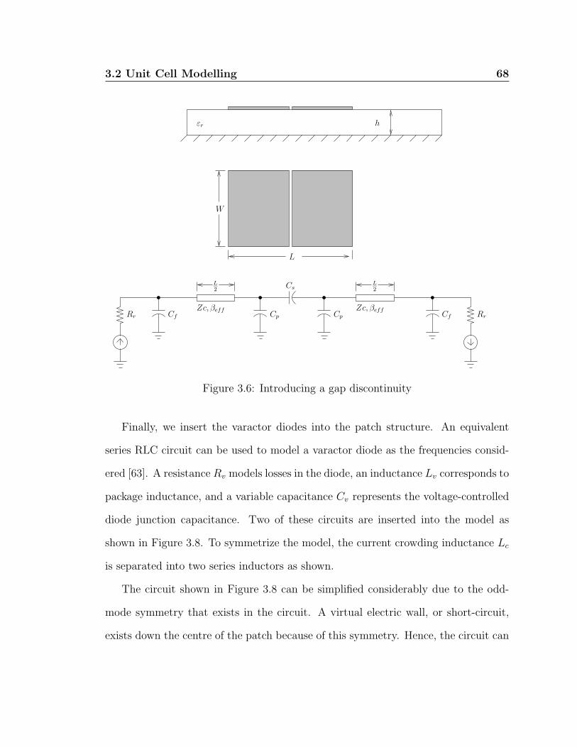
3.2 Unit Cell Modelling 68
W
L
εr h
CfRr
Zc, βeff
L2
Cp Cp
Cs
RrCf
L2
Zc, βeff
Figure 3.6: Introducing a gap discontinuity
Finally, we insert the varactor diodes into the patch structure. An equivalent
series RLC circuit can be used to model a varactor diode as the frequencies consid-
ered [63]. A resistance Rv models losses in the diode, an inductance Lv corresponds to
package inductance, and a variable capacitance Cv represents the voltage-controlled
diode junction capacitance. Two of these circuits are inserted into the model as
shown in Figure 3.8. To symmetrize the model, the current crowding inductance Lc
is separated into two series inductors as shown.
The circuit shown in Figure 3.8 can be simplified considerably due to the odd-
mode symmetry that exists in the circuit. A virtual electric wall, or short-circuit,
exists down the centre of the patch because of this symmetry. Hence, the circuit can

3.2 Unit Cell Modelling 69
CfRr
Zc, βeff
L2
Cp Cp
Cs
RrCf
L2
Zc, βeff
Lc
W
L
εr h
Figure 3.7: Modelling current crowding effects
be reduced down to that shown in Figure 3.9(a), which can be further simplified to
the form shown in Figure 3.9(b). This simple circuit can then be used to calculate
the scattering from the unit cell.
3.2.2 Computational Electromagnetics Model
The scattering characteristics of the unit cell can also be computed using a com-
putational electromagnetics approach. For this analysis, the finite-difference time-
domain (FDTD) technique [64] was employed. A unit cell was simulated using
∆x = ∆y = ∆z = 0.25 mm in the simulation. Perfect electrical conductors (PECs)
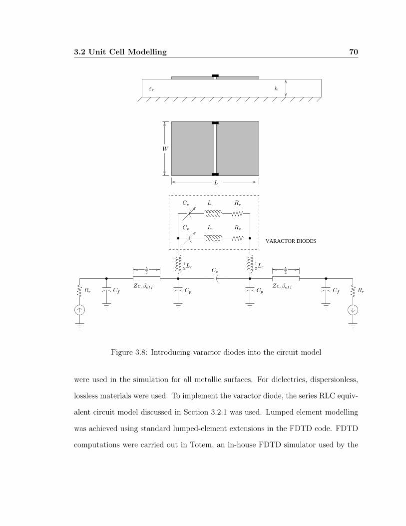
3.2 Unit Cell Modelling 70
VARACTOR DIODES
W
L
εr h
Cv RvLv
Cv RvLv
Cs
CfRr
Zc, βeff
L2
Cp Cp RrCf
L2
Zc, βeff
12Lc
12Lc
Figure 3.8: Introducing varactor diodes into the circuit model
were used in the simulation for all metallic surfaces. For dielectrics, dispersionless,
lossless materials were used. To implement the varactor diode, the series RLC equiv-
alent circuit model discussed in Section 3.2.1 was used. Lumped element modelling
was achieved using standard lumped-element extensions in the FDTD code. FDTD
computations were carried out in Totem, an in-house FDTD simulator used by the

3.2 Unit Cell Modelling 71
CfRr
Zc, βeff
L2
12Lc
4Cv14Rv
14Lv
Cp
2Cs
(a)
CfRr
Zc, βeff
L2
Cp + 2Cs
4Cv14Rv
14Lv + 1
2Lc
(b)
Figure 3.9: Simplified equivalent circuit
research group.
To determine the scattered field unit cell, it was placed at the end of a parallel-
plate waveguide (PPWG) in the simulation as shown in Figure 3.10. Boundary
conditions in the yz-plane are set to electric walls while boundary conditions in
the xy-plane are set to magnetic walls. An electric wall terminates the waveguide
while perfectly matched layer (PML) [64] is used at the input side to the waveguide.
With the PPWG dimensions chosen to be equal to that of unit cell in the array,
the technique can be used to simulate normal incidence on the patch in an infinite-
array scenario. Essentially, the electric and magnetic wall boundary conditions in the
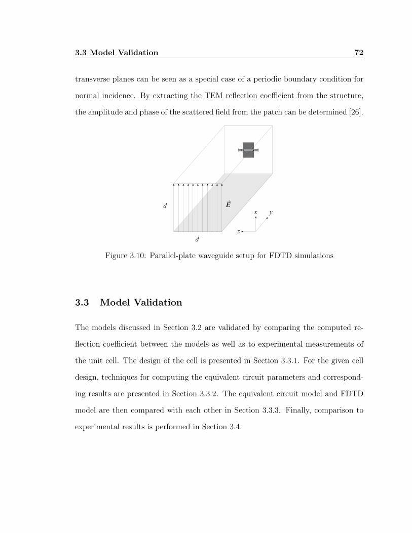
3.3 Model Validation 72
transverse planes can be seen as a special case of a periodic boundary condition for
normal incidence. By extracting the TEM reflection coefficient from the structure,
the amplitude and phase of the scattered field from the patch can be determined [26].
Figure 3.10: Parallel-plate waveguide setup for FDTD simulations
3.3 Model Validation
The models discussed in Section 3.2 are validated by comparing the computed re-
flection coefficient between the models as well as to experimental measurements of
the unit cell. The design of the cell is presented in Section 3.3.1. For the given cell
design, techniques for computing the equivalent circuit parameters and correspond-
ing results are presented in Section 3.3.2. The equivalent circuit model and FDTD
model are then compared with each other in Section 3.3.3. Finally, comparison to
experimental results is performed in Section 3.4.

3.3 Model Validation 73
3.3.1 Cell Design Details
The unit cell itself was designed at 5.5 GHz on a h = 1.524 mm substrate with
dielectric constant εr = 3.02 and loss tangent tan δ = 0.0016. The cell spacing was
chosen as d = 30 mm which corresponds to just over half a wavelength at 5.5 GHz
(d/λ0 = 0.55).
The cell was designed around a commercially available varactor tuning diode
available from MCE Metelics. A MGV-100-20 gallium arsenide (GaAs) varactor
diode was chosen for the design [65], since it offered the lowest loss in commercially
available tuning diodes. It develops a capacitance of 1.80–0.12 pF between 0–20 V
of reverse bias voltage. To determine the optimal patch dimensions, numerical ex-
periments were used to determine an ideal patch size. The maximum phase range
of the circuit, though ultimately limited by the capacitance range of the varactor
diode, can be achieved provided the diode covers most of curved part of the phase
transition in the phase versus capacitance characteristic shown in Figure 3.2. This
amounts to selecting patch dimensions such that resonance is achieved in the circuit
in Figure 3.9(b) at a reasonably low bias voltage (≤ 30 V), while providing the el-
ement with other desirable characteristics such as a usable phase slope and decent
bandwidth.
Good scattering characteristics were obtained with patch dimensions of W =
14 mm and L = 19 mm. A gap of g = 0.5 mm was used to accommodate the
varactor diode. The selected varactor diode achieves this while maintaining good
tuning characteristics, as will be discussed in more detail in Section 3.4.

3.3 Model Validation 74
3.3.2 Equivalent Circuit Parameter Computations
Before the circuit model of Section 3.2.1 can be evaluated, the parameters Cs, Cp,
Lc, Cf , and Rr must be determined for the patch geometry discussed. All of these
parameters were de-embedded from electromagnetic simulations of microstrip trans-
mission line circuits with transmission line geometry matching that of the patch
antenna. While closed-form approximations exist for Cf and Rr from the microstrip
transmission line model of the patch antenna [61], they do not account for the prox-
imity of other nearby array elements. Furthermore, while closed-form expressions
for the gap discontinuity are available, accurate forms for wide microstrip widths
are not. Finally, Lc must be de-embedded from electromagnetic simulations of the
discontinuity due to its unique geometry.
Based on these facts, electromagnetic simulations of microstrip discontinuities
were performed and the parameters de-embedded from these simulations. Totem
was used for these simulations. A microstrip line having the same width W as the
patch was excited with a microstrip mode, and the scattering parameters of the dis-
continuity of interest analyzed. These simulation results were imported into Agilent
Advanced Design SystemTM(ADS), where they were compared to ideal scattering pa-
rameters from the equivalent circuit of the discontinuity. The optimization feature
in ADS was used to arrive at circuit parameter values.
To obtain the fringing capacitance Cf , an open-end microstrip transmission line
was simulated to obtain Cf . An electric wall normal to the direction of propagation,
located a distance d/2 − L/2 from the end of the microstrip line, was included in
the simulation to produce a boundary condition approximating the infinite array
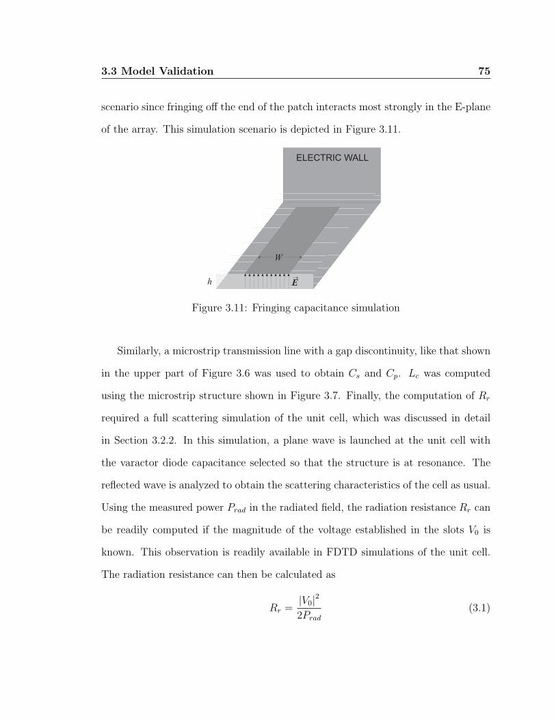
3.3 Model Validation 75
scenario since fringing off the end of the patch interacts most strongly in the E-plane
of the array. This simulation scenario is depicted in Figure 3.11.
Figure 3.11: Fringing capacitance simulation
Similarly, a microstrip transmission line with a gap discontinuity, like that shown
in the upper part of Figure 3.6 was used to obtain Cs and Cp. Lc was computed
using the microstrip structure shown in Figure 3.7. Finally, the computation of Rr
required a full scattering simulation of the unit cell, which was discussed in detail
in Section 3.2.2. In this simulation, a plane wave is launched at the unit cell with
the varactor diode capacitance selected so that the structure is at resonance. The
reflected wave is analyzed to obtain the scattering characteristics of the cell as usual.
Using the measured power Prad in the radiated field, the radiation resistance Rr can
be readily computed if the magnitude of the voltage established in the slots V0 is
known. This observation is readily available in FDTD simulations of the unit cell.
The radiation resistance can then be calculated as
Rr =|V0|
2
2Prad(3.1)

3.3 Model Validation 76
With all the microstrip discontinuities accounted for, the circuit model of Fig-
ure 3.9(b) can be evaluated once the varactor diode parameters are known.
3.3.3 Model Results
To evaluate both models of the unit cell, equivalent parameters for the RLC model
of the varactor diode are needed for both the FDTD simulations and circuit simu-
lations. Initially, these parameters were based on those published for high-Q chip
capacitors which were used for experimental measurements in Section 3.4, since it
was easiest to validate the model with a experiment with known capacitors. The
package inductance was set to Lv = 0.4 nH, which corresponds to published pack-
age inductances for the package selected. The equivalent series resistance was set
to Rv = 0.7 Ω. Equivalent circuit parameters for varactor diodes were also be used
after the initial model was validated. The package inductance remained unchanged,
and the Rv value increased to Rv = 1.45 Ω, based on the published Q of the varactor
diode used.
Although the cell was ultimately designed on a 1.5 mm substrate as presented,
several substrate heights were simulated to test the models. The results of equiv-
alent circuit parameter de-embedding discussed in Section 3.3.2 are summarized in
Table 3.1. These parameters were substituted into the circuit model of Figure 3.9(b).
The simulated scattering of the cell compared to direct FDTD scattering simula-
tions of the cell at 5.5 GHz in Figure 3.12. The results in the upper plot demonstrate
that it is indeed possible to extend the phase agility of a reflectarray cell so that close
to 360 of phase range is possible. In fact, for the h = 1.5 mm case, 345.5 of phase
range was achieved assuming the capacitor could be tuned from 0-1 pF. A more

3.3 Model Validation 77
Parameter h = 1.0 mm h = 1.5 mm h = 2.0 mm
Cs 0.348 pF 0.376 pF 0.401 pFCp 0.0215 pF 0.0341 pF 0.0450 pF12Lc 0.248 nH 0.317 nH 0.340 nHCf 0.265 pF 0.265 pF 0.268 pFRr 347 Ω 285 Ω 246 Ω
Table 3.1: Equivalent circuit parameters for various substrate heights
realistic range of 326.1 is achieved assuming a 5:1 capacitance change (0.2-1 pF),
achievable with most GaAs tuning diodes.
The phase tuning characteristic is also quite desirable for this particular design,
since the phase slope is not excessive. Excessive phase slope leads to problematic
electronic control of the element for a few reasons. First, a high slope will exaggerate
drift in the bias voltage caused by imperfect electronics. More importantly, if a
digital-to-analog converter (DAC) is used to create the bias voltage, a high phase
slope will yield very coarse discretization of the phase characteristic where the useful
range of the device lies. Finally, a high phase slope is usually indicative of a highly
resonant, low-bandwidth patch that will only work over a limited frequency range
before the phasing characteristic is completely different. Hence, phase errors will be
created in the aperture for a smaller departure from the design frequency compared
to an element with less phase slope. High phase slope also causes the element to
be very sensitive to manufactured patch dimensions and diode variations, which can
make open-loop control of the reflectarray very difficult.
As expected, as the height of the substrate is changed, the phase slope and ranges
change. Thinner substrates normally lead to more narrowband patch performance,
which manifests itself as a high-slope transition in the phase characteristic. The
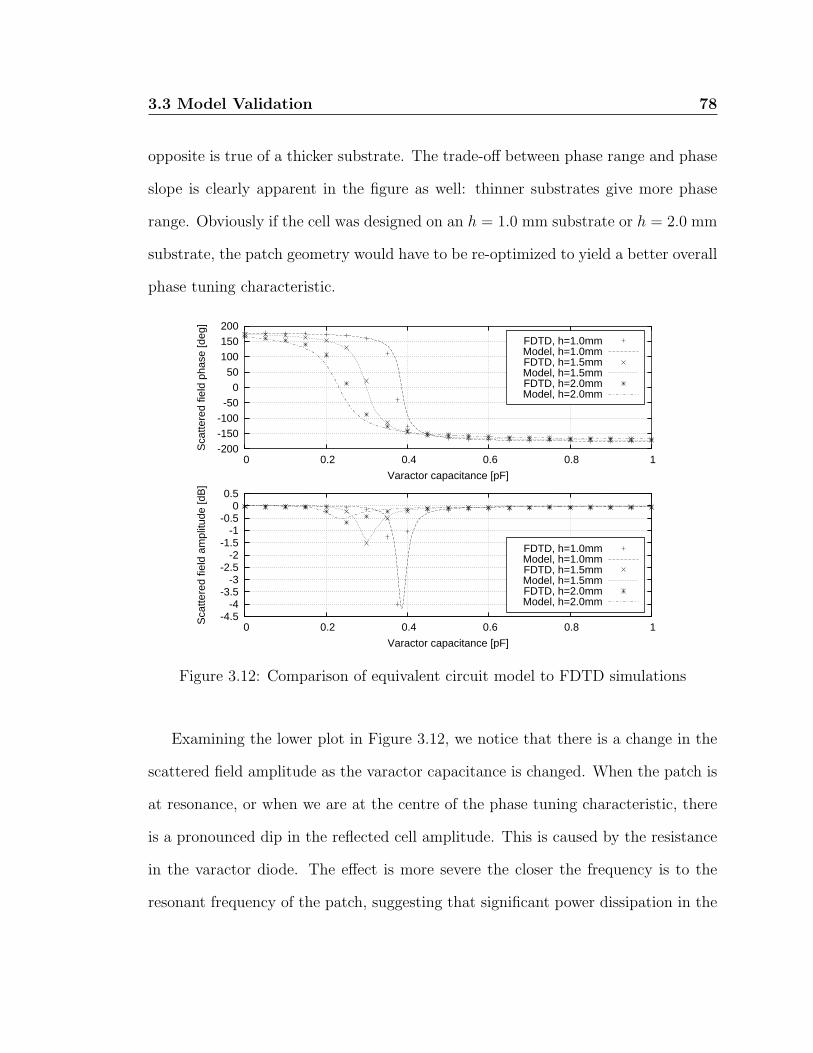
3.3 Model Validation 78
opposite is true of a thicker substrate. The trade-off between phase range and phase
slope is clearly apparent in the figure as well: thinner substrates give more phase
range. Obviously if the cell was designed on an h = 1.0 mm substrate or h = 2.0 mm
substrate, the patch geometry would have to be re-optimized to yield a better overall
phase tuning characteristic.
-4.5-4
-3.5-3
-2.5-2
-1.5-1
-0.5 0
0.5
0 0.2 0.4 0.6 0.8 1Sca
ttere
d fie
ld a
mpl
itude
[dB
]
Varactor capacitance [pF]
FDTD, h=1.0mmModel, h=1.0mmFDTD, h=1.5mmModel, h=1.5mmFDTD, h=2.0mmModel, h=2.0mm
-200-150-100-50
0 50
100 150 200
0 0.2 0.4 0.6 0.8 1
Sca
ttere
d fie
ld p
hase
[deg
]
Varactor capacitance [pF]
FDTD, h=1.0mmModel, h=1.0mmFDTD, h=1.5mmModel, h=1.5mmFDTD, h=2.0mmModel, h=2.0mm
Figure 3.12: Comparison of equivalent circuit model to FDTD simulations
Examining the lower plot in Figure 3.12, we notice that there is a change in the
scattered field amplitude as the varactor capacitance is changed. When the patch is
at resonance, or when we are at the centre of the phase tuning characteristic, there
is a pronounced dip in the reflected cell amplitude. This is caused by the resistance
in the varactor diode. The effect is more severe the closer the frequency is to the
resonant frequency of the patch, suggesting that significant power dissipation in the

3.4 Experimental Measurements of the Unit Cell 79
varactor diode is occurring at this point. Part of the optimization process is to ensure
that this loss is not too great, since power lost in the diode will ultimately reduce
the reflector efficiency of the reflectarray.
In both the phase and amplitude plots, we notice excellent correlation between
the equivalent circuit model and the computational electromagnetics model. Hence,
both tools have excellent potential as design tools for reflectarray elements. The
circuit model has an advantage of being simpler and faster to evaluate, provided
that circuit parameters for the discontinuities are known. However, even with rough
estimates of these parameters, the circuit model can be used to produce a basic
design of a unit cell, and then the cell can be further optimized through the use of
electromagnetic simulations. The circuit model can also be used to predict important
tuning parameters such as phase range, phase slope, and bandwidth.
The effect of changing Rv is illustrated in Figure 3.13. Only the amplitude
response of the unit cell is shown, since changing Rv produces negligible changes in
the scattered field phase unless Rv is large. One can notice that there is a strong
sensitivity to the amplitude response to the series resistance of the diode. Changing
the resistance to a realistic value for varactor diodes increases the loss to over 3 dB
at resonance, which is quite pronounced.
3.4 Experimental Measurements of the Unit Cell
To measure the scattered field from the element, a slightly different setup was used,
since a high-quality air-filled PPWG with the dimensions shown could not be prac-
tically realized. Instead, the element was placed at the end of a section of rectan-
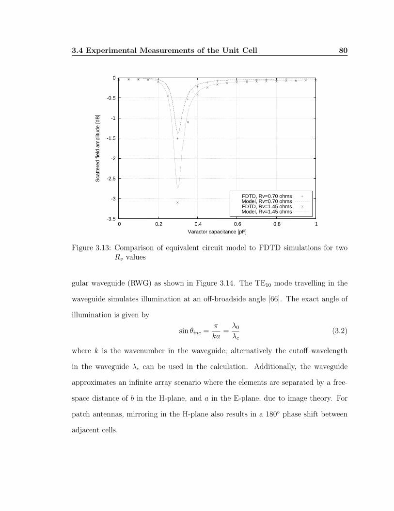
3.4 Experimental Measurements of the Unit Cell 80
-3.5
-3
-2.5
-2
-1.5
-1
-0.5
0
0 0.2 0.4 0.6 0.8 1
Sca
ttere
d fie
ld a
mpl
itude
[dB
]
Varactor capacitance [pF]
FDTD, Rv=0.70 ohmsModel, Rv=0.70 ohmsFDTD, Rv=1.45 ohmsModel, Rv=1.45 ohms
Figure 3.13: Comparison of equivalent circuit model to FDTD simulations for twoRv values
gular waveguide (RWG) as shown in Figure 3.14. The TE10 mode travelling in the
waveguide simulates illumination at an off-broadside angle [66]. The exact angle of
illumination is given by
sin θinc =π
ka=λ0
λc(3.2)
where k is the wavenumber in the waveguide; alternatively the cutoff wavelength
in the waveguide λc can be used in the calculation. Additionally, the waveguide
approximates an infinite array scenario where the elements are separated by a free-
space distance of b in the H-plane, and a in the E-plane, due to image theory. For
patch antennas, mirroring in the H-plane also results in a 180 phase shift between
adjacent cells.
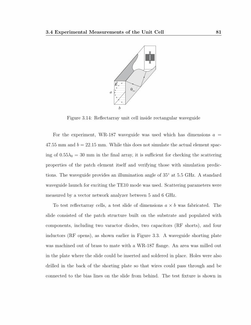
3.4 Experimental Measurements of the Unit Cell 81
Figure 3.14: Reflectarray unit cell inside rectangular waveguide
For the experiment, WR-187 waveguide was used which has dimensions a =
47.55 mm and b = 22.15 mm. While this does not simulate the actual element spac-
ing of 0.55λ0 = 30 mm in the final array, it is sufficient for checking the scattering
properties of the patch element itself and verifying those with simulation predic-
tions. The waveguide provides an illumination angle of 35 at 5.5 GHz. A standard
waveguide launch for exciting the TE10 mode was used. Scattering parameters were
measured by a vector network analyzer between 5 and 6 GHz.
To test reflectarray cells, a test slide of dimensions a × b was fabricated. The
slide consisted of the patch structure built on the substrate and populated with
components, including two varactor diodes, two capacitors (RF shorts), and four
inductors (RF opens), as shown earlier in Figure 3.3. A waveguide shorting plate
was machined out of brass to mate with a WR-187 flange. An area was milled out
in the plate where the slide could be inserted and soldered in place. Holes were also
drilled in the back of the shorting plate so that wires could pass through and be
connected to the bias lines on the slide from behind. The test fixture is shown in

3.4 Experimental Measurements of the Unit Cell 82
Figure 3.15(a) and a photo of the setup is shown in Figure 3.15(b).
(a) Test fixture (b) Photo
Figure 3.15: Experimental characterization of unit cells using rectangular waveguide
3.4.1 Fixed Capacitor Cell Results
As an initial test, fixed capacitors were soldered in place of the varactor diodes on
the test slide. Standard surface mount, high-Q capacitors in an 0402 package were
used, which have equivalent circuit parameters described earlier. Capacitor values
were available from 0.1 pF to 1 pF in 0.05-0.1 pF steps. Each capacitor was soldered
to the test slide and the reflection coefficient of the test slide measured.
To provide a comparison to experimental results, the computational model dis-
cussed in Section 3.2.2 was modified so that simulation inside a rectangular waveguide
could be performed. This amounted to changing the boundary conditions in the yz-
planes to electric walls instead of magnetic walls. The same circuit parameters were
used for the varactor diode model in the simulation.
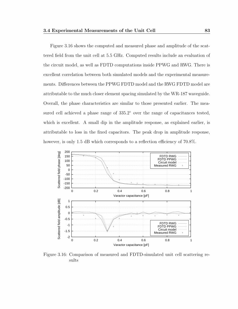
3.4 Experimental Measurements of the Unit Cell 83
Figure 3.16 shows the computed and measured phase and amplitude of the scat-
tered field from the unit cell at 5.5 GHz. Computed results include an evaluation of
the circuit model, as well as FDTD computations inside PPWG and RWG. There is
excellent correlation between both simulated models and the experimental measure-
ments. Differences between the PPWG FDTD model and the RWG FDTD model are
attributable to the much closer element spacing simulated by the WR-187 waveguide.
Overall, the phase characteristics are similar to those presented earlier. The mea-
sured cell achieved a phase range of 335.2 over the range of capacitances tested,
which is excellent. A small dip in the amplitude response, as explained earlier, is
attributable to loss in the fixed capacitors. The peak drop in amplitude response,
however, is only 1.5 dB which corresponds to a reflection efficiency of 70.8%.
-2
-1.5
-1
-0.5
0
0.5
1
0 0.2 0.4 0.6 0.8 1Sca
ttere
d fie
ld a
mpl
itude
[dB
]
Varactor capacitance [pF]
FDTD RWGFDTD PPWGCircuit model
Measured RWG
-200-150-100-50
0 50
100 150 200
0 0.2 0.4 0.6 0.8 1
Sca
ttere
d fie
ld p
hase
[deg
]
Varactor capacitance [pF]
FDTD RWGFDTD PPWGCircuit model
Measured RWG
Figure 3.16: Comparison of measured and FDTD-simulated unit cell scattering re-sults
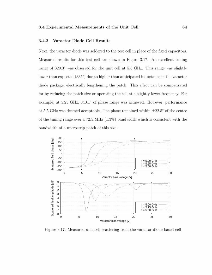
3.4 Experimental Measurements of the Unit Cell 84
3.4.2 Varactor Diode Cell Results
Next, the varactor diode was soldered to the test cell in place of the fixed capacitors.
Measured results for this test cell are shown in Figure 3.17. An excellent tuning
range of 320.3 was observed for the unit cell at 5.5 GHz. This range was slightly
lower than expected (335) due to higher than anticipated inductance in the varactor
diode package, electrically lengthening the patch. This effect can be compensated
for by reducing the patch size or operating the cell at a slightly lower frequency. For
example, at 5.25 GHz, 340.1 of phase range was achieved. However, performance
at 5.5 GHz was deemed acceptable. The phase remained within ±22.5 of the centre
of the tuning range over a 72.5 MHz (1.3%) bandwidth which is consistent with the
bandwidth of a microstrip patch of this size.
-8-7-6-5-4-3-2-1 0
0 5 10 15 20 25 30Sca
ttere
d fie
ld a
mpl
itude
[dB
]
Varactor bias voltage [V]
f = 5.00 GHzf = 5.25 GHzf = 5.50 GHz
-200-150-100-50
0 50
100 150 200
0 5 10 15 20 25 30
Sca
ttere
d fie
ld p
hase
[deg
]
Varactor bias voltage [V]
f = 5.00 GHzf = 5.25 GHzf = 5.50 GHz
Figure 3.17: Measured unit cell scattering from the varactor-diode based cell

3.4 Experimental Measurements of the Unit Cell 85
As shown in the lower plot of Figure 3.17, the varactor diode-based cell suffered
from considerable amplitude fluctuations about the centre of the tuning range, as
expected from earlier simulations. In practise, this loss will also be increased slightly
by the losses in the substrate and metals. However, the bulk of the loss originates
from power losses in the diode. The effect is more severe the closer the frequency is
to the resonant frequency of the structure, suggesting that significant power dissi-
pation in the varactor diode is occurring at this point. For the design frequency of
5.5 GHz, 3.5 dB of reflection loss is observable, which closely matches the reflection
loss predicted by the circuit and FDTD models. This loss corresponds to 44.7%
reflection efficiency. Though this loss is considerable, it was deemed acceptable for
the first prototype of a tunable reflectarray cell.
The loss effect can be addressed by using higher-Q diodes in the unit cell, or
perhaps through adjusting the position of the varactor diodes away from the current
maximum of the patch. As an experiment, additional diodes were added to the patch
in parallel with the existing diodes, reducing the value of their series resistance by
half. Employing this approach, the scattered amplitude was improved by more than
4.3 dB at a lower frequency of 5.0 GHz, where the loss was originally -7.3 dB. The
amount of improvement declines as the frequency is increased. However, a two-diode
design was of prime interest in this study to keep the overall component costs of the
array down.

Chapter 4
Reflectarray Analysis
Chapter 3 demonstrated a number of ways that tunable reflectarray elements
can be analyzed at the unit cell level. The next step is to understand how the
cell’s design affects the performance of the system as a whole when numerous unit
cells are assembled into an array. Similar to analyzing unit cells, at the array level,
there exists a number of techniques for predicting the performance of reflectarrays,
particularly the radiation pattern of the system as a whole. This chapter presents
several techniques for evaluating the gain of a reflectarray both mathematically and
using computational electromagnetics simulations.
Section 4.1 discusses mathematical techniques for evaluating the gain of a reflec-
tarray. Sources of loss are presented, and methods for accounting for them discussed.
The second half of the chapter focuses on numerical techniques for predicting specu-
lar reflection losses and other reflectarray effects. Results from these simulations are
presented near the end of the chapter.
4.1 Evaluating Reflectarray Gain
4.1.1 Reflectarray Gain
As presented in Chapter 2, reflectarrays share properties of both reflectors and an-
tenna arrays. Even though the analysis techniques are slightly different for both
types of antennas, either one can be used to compute characteristics of the reflectar-

4.1 Evaluating Reflectarray Gain 87
ray antenna. The gain of a reflectarray is one example.
From reflector antenna theory, we know that the maximum gain achievable from
a large aperture is given by equation (2.64), which is directly proportional to the
area of the antenna’s subtended aperture. If we now consider a reflectarray, with
unit cell dimensions d × d, assembled from N elements into a rectangular, planar
array, the maximum gain achievable from such a reflector is given as
Gmax =4π
λ20
Ap =4π
λ20
Nd2 (4.1)
since the area of the reflectarray is Nd2. This gain expression assumes perfect aper-
ture efficiency.
It is also possible to evaluate the gain of an antenna using array theory. Sec-
tion 2.2.3 presented the technique for evaluating the directivity of an array. If we
restrict our focus to an array designed with a period of one half-wavelength, we know
the directivity of the system is given by equation (2.36), which stated that the di-
rectivity of an antenna array is simply equal to the number of elements. Hence, for
an isotropic array,
Gmax = AF = N. (4.2)
In the case of a reflectarray, or practical antenna array for that matter, non-isotropic
elements are used to realize the array. The elements themselves have gain since
they are not isotropic. Recall from equation (2.10) that the gain of a single antenna
element is given by
Ge =4π
λ20
Ae. (4.3)
If these elements are assembled into an array, then from pattern multiplication we
know that the composite radiation pattern of an array is equal to the product of the

4.1 Evaluating Reflectarray Gain 88
array factor AF and the element factor. Hence, the maximum possible gain is given
by
Gmax = N ·Gmaxe =
4π
λ20
NAe. (4.4)
Comparing equations (4.1) and (4.4) we see that they are reconciled if Ae = d2.
As we will see, for a well-designed reflectarray element, this is indeed the case and
that the gain expression for reflector antennas can be used to evaluate the gain of a
reflectarray.
In practise, the gain of the reflectarray is less that the maximum value predicted
by equation (4.1) because of factors affecting the efficiency of reflector antennas, as
discussed in detail in Section 2.3.4. A number of factors deserve particular consid-
eration when analyzing reflectarrays, because their effects can be more pronounced
for this type of reflector. Some of these effects also manifest themselves differently
than they do in classical reflectors. These factors are summarized as follows:
• Aperture phase errors. Whether producing multiple beams or a single
pencil beam, aperture phase errors can be pronounced in reflectarrays because
their constituent unit cells may be incapable of shifting the incident wave phase
over the entire 360 range. Or, phase errors may be introduced by mis-biasing
reflectarray unit cells and/or discretization effects in the bias circuitry.
• Reflectarray cell loss. In Section 3.4, is was shown that tunable reflectarray
cells do not reflect all of the incident energy perfectly. Instead, the magnitude
of the reflection is a function of where the cell is biased because of losses in the
tuning element, dielectric losses, and metal losses. Essentially, this resembles
ohmic losses in classical reflector antennas and represents a major source of

4.1 Evaluating Reflectarray Gain 89
loss for reflectarrays.
• Scanning loss. As a reflectarray is scanned off broadside, the response of the
array diminishes due to the reduced subtended aperture of the reflector, and
rolloff in the element factor of the antennas making up the reflectarray. This is
not accounted for in standard reflector antennas since they are not composed
of antenna elements.
• Surface wave losses. Surface waves can be excited by microstrip antennas
that take power away from the space wave created by the array. However, for
reflectarrays on a low-dielectric constant substrate, and with element spacing
such that grating lobes are not produced by the array, this loss should be less
than a few percent [15].
• Specular reflection loss. Unlike shaped reflectors, which are designed to
reflect incident rays from the feed along the axis of the reflector (or vice versa),
a flat reflector like a reflectarray may reflect energy in directions not corre-
sponding to the desired reflection angle. This energy is lost.
The prediction of these effects requires specialized analysis. Aperture phase errors
and amplitude effects can be predicted using array theory, if the actual phase and
amplitude response of the cells are known. A modified form of equation (2.23)
suitable for reflectarrays is
AFr(θ, φ) =N−1∑
n=0
M−1∑
m=0
Amn(θmn, φmn, ψmn)ejk0[x′mn sin θ cosφ+y′mn sin θ sinφ]ejψmn (4.5)
where ψmn is the actual phase angle produced by the mnth cell. For the case of
single beam reflectarrays, ψmn should be equal to αmn as given by equation (2.25).

4.1 Evaluating Reflectarray Gain 90
In practise, deviations from αmn will be introduced from two sources. First, there
are always manufacturing variances from cell to cell that will introduce a departure
from the known phase response of the cell. This source of error can be difficult to
characterize experimentally. The other source of error is the limited tuning range of
the reflectarray cell. In the case of the the cell topology discussed, there is always
an unachievable phase range of approximately 20 − 30. Fortunately, these phase
range of the cell is predictable, since a cell can be measured experimentally. Phase
errors introduced by the limiting tuning range of reflectarray cells usually dominate
aperture phase error for reflectarrays since cell variances can be compensated for
using closed-loop control of the reflectarray.
Amplitude variations are introduced into the aperture by two sources: feed illu-
mination taper, and losses in the reflectarray cell. These effects are also accounted
for using equation (4.5) by making the amplitude response of the cell Amn a function
of the illumination angle between the mnth element and the feed (θmn, φmn) as well
as the programmed phase angle of the cell ψmn. Illumination taper from the feed
is readily determined from electromagnetic simulations or calculations of the feed
horn’s characteristics. Losses introduced by tuning the cell can also be predicted
from measurements of an individual unit cell.
Scanning loss, the third term in the list, is perhaps the most predictable of all
the losses because the element factor Ge of the array elements is usually well-known
and readily computed. Finally, surface wave losses and specular reflection losses
can be accounted for by absorbing them into the overall aperture efficiency of the
reflectarray. The total gain of a reflectarray as a function of scan angle can then be

4.1 Evaluating Reflectarray Gain 91
computed using
Gr(θ, φ) = εapAFr ·Ge(θ, φ) (4.6)
= εapGe(θ, φ)N−1∑
n=0
M−1∑
m=0
Amn(θmn, φmn, ψmn)
ejk0[x′
mn sin θ cosφ+y′mn sin θ sinφ]ejψmn (4.7)
Specular reflection effects are perhaps the most difficult to estimate in εap be-
cause they cannot be solved using array theory. The specular reflection problem is
unique to reflectarrays, and has not been sufficiently treated in the literature. It
must be analyzed using a full-wave technique and is particularly difficult to isolate
because the reflections from the reflectarray must be mathematically separated into
the desired and undesired scattered field components. As we will see, this analysis is
facilitated through the use of a specialized FDTD technique which will be presented
in Section 4.2.
4.1.2 Element Gain
As indicated by equation (4.7), the gain of the reflectarray is dependent upon the
individual gains of the constituent microstrip elements in the reflectarray. The gain
of these elements has been well-characterized in the literature. Using a standard
cavity model of the microstrip patch antenna [61], the electric field in the far-field
can be evaluated as
Eθ(θ, φ) = sinc
(
k0W
2πsin θ sinφ
)
cos
(
k0L
2sin θ cosφ
)
cosφ (4.8)
and
Eφ(θ, φ) = −sinc
(
k0W
2πsin θ sinφ
)
cos
(
k0L
2sin θ cosφ
)
cos θ sinφ (4.9)

4.2 Infinite Reflectarray Analysis using the FDTD Technique 92
over the range 0 ≤ θ ≤ 90 for a patch in the xy-plane polarized in the x-direction.
Outside this range, the response of an ideal patch is zero since a theoretical patch
antenna is bounded by an infinite ground plane in the xy plane.
The directivity of a microstrip patch with far-field patterns described by the
above equations can be found by computing the normalized, total electric field in
the far-field:
EF (θ, φ) =
√
E 2θ (θ, φ) + E 2
φ (θ, φ)
max
(
√
E 2θ (θ, φ) + E 2
φ (θ, φ)
) (4.10)
The maximum directivity of the patch is then found from equations (2.6) and (2.7)
as
Dmaxe =
4π∫∫
|EF (θ, φ)|2dΩ(4.11)
The directivity of standard microstrip patches is usually 6-7 dB. A typical radiation
pattern produced by a patch is illustrated graphically in Figure 4.1, which shows a
broad beam in the E-plane (x-direction) and H-plane (y-direction).
4.2 Infinite Reflectarray Analysis using the FDTD Tech-
nique
The FDTD technique was used extensively in Chapter 3 to predict the scattering
properties of unit cells in a reflectarray, and to aid in understanding of scattering
dynamics of the unit cell. Similarly, the FDTD method can be used to predict
array-level performance parameters. The goal of the analysis is twofold:
1. To gain physical insight into the reflection properties of reflectarrays, such as
the transient response of the reflection process.
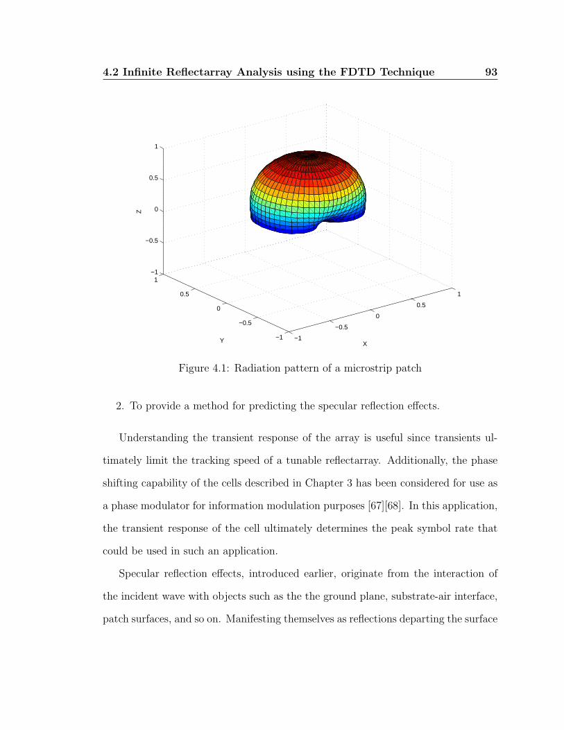
4.2 Infinite Reflectarray Analysis using the FDTD Technique 93
−1
−0.5
0
0.5
1
−1
−0.5
0
0.5
1−1
−0.5
0
0.5
1
XY
Z
Figure 4.1: Radiation pattern of a microstrip patch
2. To provide a method for predicting the specular reflection effects.
Understanding the transient response of the array is useful since transients ul-
timately limit the tracking speed of a tunable reflectarray. Additionally, the phase
shifting capability of the cells described in Chapter 3 has been considered for use as
a phase modulator for information modulation purposes [67][68]. In this application,
the transient response of the cell ultimately determines the peak symbol rate that
could be used in such an application.
Specular reflection effects, introduced earlier, originate from the interaction of
the incident wave with objects such as the the ground plane, substrate-air interface,
patch surfaces, and so on. Manifesting themselves as reflections departing the surface
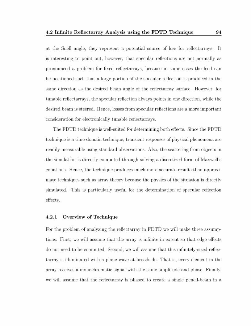
4.2 Infinite Reflectarray Analysis using the FDTD Technique 94
at the Snell angle, they represent a potential source of loss for reflectarrays. It
is interesting to point out, however, that specular reflections are not normally as
pronounced a problem for fixed reflectarrays, because in some cases the feed can
be positioned such that a large portion of the specular reflection is produced in the
same direction as the desired beam angle of the reflectarray surface. However, for
tunable reflectarrays, the specular reflection always points in one direction, while the
desired beam is steered. Hence, losses from specular reflections are a more important
consideration for electronically tunable reflectarrays.
The FDTD technique is well-suited for determining both effects. Since the FDTD
technique is a time-domain technique, transient responses of physical phenomena are
readily measurable using standard observations. Also, the scattering from objects in
the simulation is directly computed through solving a discretized form of Maxwell’s
equations. Hence, the technique produces much more accurate results than approxi-
mate techniques such as array theory because the physics of the situation is directly
simulated. This is particularly useful for the determination of specular reflection
effects.
4.2.1 Overview of Technique
For the problem of analyzing the reflectarray in FDTD we will make three assump-
tions. First, we will assume that the array is infinite in extent so that edge effects
do not need to be computed. Second, we will assume that this infinitely-sized reflec-
tarray is illuminated with a plane wave at broadside. That is, every element in the
array receives a monochromatic signal with the same amplitude and phase. Finally,
we will assume that the reflectarray is phased to create a single pencil-beam in a

4.2 Infinite Reflectarray Analysis using the FDTD Technique 95
non-broadside direction. This will enable both goals to be accomplished. By phas-
ing the reflection to an off-broadside angle, separating the reflection from a specular
reflection in the transient observations of the array will become easier. Additionally,
by observing any remaining reflections at broadside, we will have isolated the spec-
ular reflection of the reflectarray, because any energy not re-directed by the array
is reflected at the Snell angle, which is in the direction of the incoming wave for
broadside incidence.
To establish a single beam for a 2-D planar array, recall from equation (2.25) that
this requires a phase gradient to be established along the array elements. The actual
phase gradient is periodic since phase values are modulo-360. Hence, an infinite
array is actually an assembly of an infinite number of periods of structures phased to
produce the desired beam. Analyzing one period of this structure, then, can be used
to analyze an infinite array because only knowledge of a single period is required to
predict the behaviour of the rest of the array.
Consider the case of reflecting an incident beam so that it is re-directed in one of
the principal planes of the array. Then, the phase gradient of the array is established
along only one of the array’s two principal axes, allowing us to simplify our analysis
to a 1-D array. An example of this situation is illustrated in Figure 4.2, which
shows a 4×1 period of the array based on the reflectarray cell topology presented in
Chapter 3. The section of reflectarray is bounded by periodic boundary conditions in
the xy-planes and the yz-planes, so that an infinite array extending infinitely in the
x- and z-directions is produced. The array is phased so that periodicity is maintained
in the z-direction as shown in the figure, while covering a 360 phase gradient across
the aperture. Broadside excitation is produced in an excitation plane at the entrance
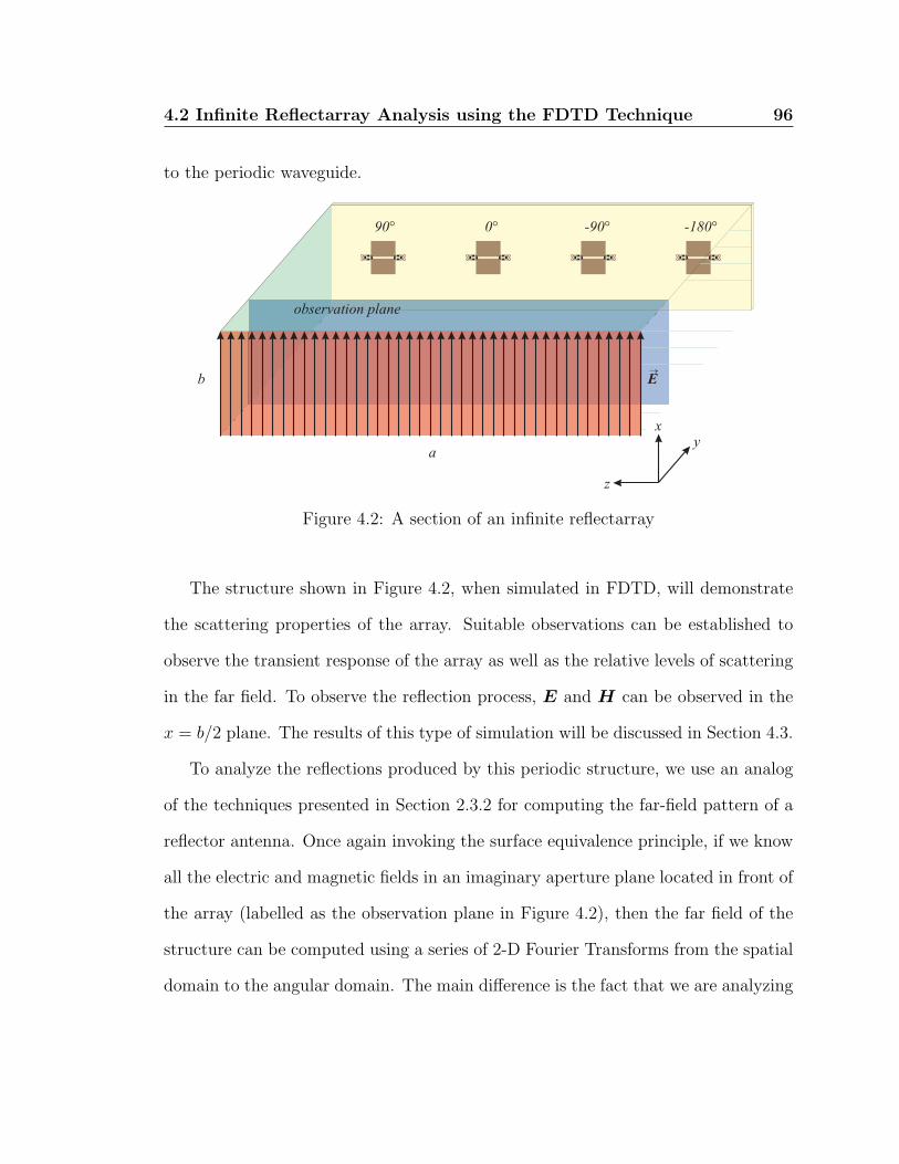
4.2 Infinite Reflectarray Analysis using the FDTD Technique 96
to the periodic waveguide.
Figure 4.2: A section of an infinite reflectarray
The structure shown in Figure 4.2, when simulated in FDTD, will demonstrate
the scattering properties of the array. Suitable observations can be established to
observe the transient response of the array as well as the relative levels of scattering
in the far field. To observe the reflection process, E and H can be observed in the
x = b/2 plane. The results of this type of simulation will be discussed in Section 4.3.
To analyze the reflections produced by this periodic structure, we use an analog
of the techniques presented in Section 2.3.2 for computing the far-field pattern of a
reflector antenna. Once again invoking the surface equivalence principle, if we know
all the electric and magnetic fields in an imaginary aperture plane located in front of
the array (labelled as the observation plane in Figure 4.2), then the far field of the
structure can be computed using a series of 2-D Fourier Transforms from the spatial
domain to the angular domain. The main difference is the fact that we are analyzing

4.2 Infinite Reflectarray Analysis using the FDTD Technique 97
a periodic section of an aperture instead of the entire aperture, the implications of
which will be discussed in more detail shortly. We first turn our attention to the
technique used to establish far-field quantities from the reflectarray.
4.2.2 Computation of Far-Field Radiation Pattern
The computation of the far-field radiation pattern from an aperture antenna requires
knowledge of the electric and magnetic fields everywhere in the aperture. With
the use of the FDTD technique, this information is readily observable, and the
far-field radiation pattern readily computed from the well-known near-to-far-field
transformation in FDTD [64]. With some minor changes, this technique can be
applied to the situation shown in Figure 4.2. Before that, let us briefly review the
operations involved in the near-to-far-field transformation.
The Near-to-Far-Field Transformation
From Section 2.3.2, we know that the vector potentials for the magnetic and electric
fields are given by equations (2.48) and (2.49). We can redefine these equations so
that
A = µ0e−jk0r
4πr
∫∫
S
Js(r′)ejk0r·r′
dS ′ = µ0e−jk0r
4πrN (4.12)
and
F = εe−jk0r
4πr
∫∫
S
Ms(r′)ejk0r·r′
dS ′ = εe−jk0r
4πrL (4.13)
where
N =
∫∫
S
Js(r′)ejk0r·r′
dS ′ =
∫∫
S
Js(r′)ejk0r
′ cosψdS ′, (4.14)
L =
∫∫
S
Ms(r′)ejk0r·r′
dS ′ =
∫∫
S
Ms(r′)ejk0r
′ cosψdS ′, (4.15)

4.2 Infinite Reflectarray Analysis using the FDTD Technique 98
and cosψ = r · r′. Then, the equivalent forms of the far field expressions of equa-
tions (2.55) and (2.56) in spherical coordinates are given by
Eθ = jk0e−jk0r
4πr(Lφ + ηNθ) (4.16)
and
Eφ = jk0e−jk0r
4πr(Lθ − ηNφ) (4.17)
For the case of FDTD simulations performed in Cartesian space, the near-to-far-
field transformation proceeds as follows. The electric and magnetic fields are recorded
in six imaginary apertures corresponding the the six boundaries of the cube-shaped
simulation space. The equivalent magnetic and electric currents flowing surfaces are
used to compute the far-field pattern of the structure within the cube thanks to the
surface equivalence principle. For equivalent electric and magnetic currents flowing
on these surfaces, the spherical components of the N - and L− integrals become
Nθ =
∫∫
S
(Jx cos θ cosφ+ Jy cos θ sinφ− Jz sin θ)ejk0r′ cosψdS ′ (4.18)
Nφ =
∫∫
S
(−Jx sinφ+ Jy cosφ)ejk0r′ cosψdS ′ (4.19)
Lθ =
∫∫
S
(Mx cos θ cosφ+My cos θ sinφ−Mz sin θ)ejk0r′ cosψdS ′ (4.20)
Lφ =
∫∫
S
(−Mx sinφ+My cosφ)ejk0r′ cosψdS ′ (4.21)
Each of these integrals is evaluated for each of the six faces used in the near-to-far-
field transformation. However, in the case of an infinite array in the xz-plane, and the
associated period being analyzed, we only require that the fields in the observation
plane shown in Figure 4.2 be evaluated because of the structure of the simulations.
Hence, for an observation plane located at y = y0, Jy = My = 0 and the exponential

4.2 Infinite Reflectarray Analysis using the FDTD Technique 99
phase term in the L and N integrals reduces to
r′ cosψ = x′ sin θ cosφ+ y0 sin θ sinφ+ z′ cos θ (4.22)
Thus, from the four integrations weighted according to equations (4.16) and (4.17),
the far-field of an infinite reflectarray can be computed. The equivalent surface
currents are computed from measurements of E and H in the reflector aperture in an
FDTD simulation using equations (2.46) and (2.47). Standard averaging techniques
used in FDTD are used to interpolate E- and H- values in the FDTD grid [64].
Far-Fields of a Periodic Aperture
As mentioned earlier, the size of the entire aperture in this analysis is infinite since
the reflectarray is infinite in extent. By focusing on the behaviour of a single period of
this structure, the behaviour of the array as a whole can be predicted. However, there
are differences between analyzing a finite-sized aperture and a finite-sized aperture
representing one period of an infinite structure. In the case of a finite aperture,
such as that used in the standard near-to-far-field transform, the two-dimensional
Fourier Transform is used to transform aperture fields from the spatial domain to
the angular domain (the far field), where the resultant far-field electric and magnetic
fields potentially exist for all angles. However, the aperture under consideration in
this case represents one period of an infinite, periodic aperture. Hence, a Fourier
Series can be used to represent the aperture field quantities J and M , implying
that the resultant far-field quantities will only exist at discrete angles. For the one-
dimensional case shown in Figure 4.2, we can define the independent variable in the
angular domain as
u = cos θ. (4.23)

4.2 Infinite Reflectarray Analysis using the FDTD Technique 100
Since the fundamental “frequency” at which the aperture repeats in the z-direction
is u = λ0
a, the far field quantities will then exist at discrete angles defined by
nu0 = nλ0
a(4.24)
where: a is the length of the period of the aperture distribution as defined in Fig-
ure 4.2 and n is an integer. The number of discrete radiation angles (or spectra)
that can be computed from considering one period of the aperture is constrained
such that |u| ≤ 1, since | cos θ| ≤ 1 for real-valued angles θ. Hence
−1 ≤ nλ0
a≤ 1 (4.25)
or
n ≤
∣
∣
∣
∣
a
λ0
∣
∣
∣
∣
(4.26)
which says that n must be less than the period of the aperture in wavelengths.
For complex aperture distributions, several spectra may exist in the angular do-
main, which translates to a larger period in the spatial domain. Conversely, for
an aperture that consists of an ideal phase gradient, only one spectral component
will exist (i.e., a pencil beam). The angle of radiation is computed by considering
a one-dimensional infinite array with an unnormalized array factor given by equa-
tion (2.19):
AF =∞∑
n=−∞
ejk0nd cos θ−jnα (4.27)
where: d is the element spacing and α is the inter-element phase shift. Then,
AF = 1 +∞∑
n=1
(
e−jn(k0d cos θ−α) + ejn(k0d cos θ−α))
(4.28)
= 1 + 2∞∑
n=1
cos[n(k0d cos θ − α)]. (4.29)

4.2 Infinite Reflectarray Analysis using the FDTD Technique 101
Normalizing by 2π:
AF
2π=
1
2π+
1
π
∞∑
n=1
cos[n(k0d cos θ − α)] (4.30)
AF
2π=
1
2π+
1
π
∞∑
n=1
cos[n(k0du− α)] (4.31)
= δ
(
u−α
k0d
)
(4.32)
where δ(u) is a Dirac delta function in the angular domain. Hence, an infinite array
phased with an inter-element phasing produces a beam at
u =α
k0d(4.33)
If the inter-element phase shift α is set such that for a periodic aperture containing
N elements,
α =2π
N(4.34)
then
u =2π
N
1
k0d=
λ0
Nd(4.35)
which corresponds to the 1st harmonic (n = 1) in equation (4.24) since a = Nd.
For example, for the situation shown in Figure 4.2, α = 90 and the reflectarray
will re-direct an incident beam 27 degrees off broadside to θ = 63 in the H-plane
(yz-plane).
Hence, one potential method to analyze the specular reflection produced by an
infinite reflectarray is to phase the array for a single pencil-beam. By evaluating
components at n = 0 (broadside angle) and n = 1 (phased angle) in the angu-
lar spectrum of the aperture distribution, the levels of reflection produced in the
dominant reflection angles of the reflectarray can be predicted.

4.2 Infinite Reflectarray Analysis using the FDTD Technique 102
The technique just presented for predicting the amount of specular reflection is
theoretically sound. Practically, however, it is a computationally demanding pro-
cedure. The reason becomes apparent when the work flow for such a simulation is
considered. The workflow is as follows:
1. Simulate the single unit cell configurations necessary to produce unit cells
with the desired phasing characteristics. For example, for the case shown in
Figure 4.2, determine which unit cells will produce scattered field phase angles
of 90, 0, −90, and −180.
2. Assemble the unit cells into the sub-array representing one period of the struc-
ture and complete a scattering simulation of the structure.
3. Perform the modified near-to-far-field transformation to compute the amount
of reflections produced at the angles of interest.
The second step of the process is potentially the most computationally expensive.
As opposed to FDTD simulations of a unit cell, the simulation requires N times
more cells, where N is the number of reflectarray elements used in the sub-array.
Though the computation complexity of FDTD is only O(N), the need to simulate N
cells imposes limitations on the maximum unit cell size that can be simulated since
the unit cell is limited to one-Nth the size of the maximum simulation size.
The technique is also sensitive to phase errors introduced when cells configured
for certain scattering properties are assembled into an array. Interaction between
the cells alters their scattering behaviour due to mutual coupling effects. Hence, the
structure may require several iterations as the varactor capacitances are fine-tuned
to yield proper phasing of the array.

4.2 Infinite Reflectarray Analysis using the FDTD Technique 103
There is a simpler way of predicting specular reflection effects based on simula-
tions of a single unit cell. The technique works as follows. Consider the reflection
produced by a unit cell excited at broadside, which is produced in the far field at
θ = 90, φ = −90. By superposition, this field consists of two components, as
described by the equation
E(θ = 90, φ = −90, ψ) = Es(θ = 90, φ = −90, ψ) + Er (4.36)
where: Es is the scattered field phased at an angle ψ produced by the patch antenna,
and Er is the reflected field produced by specular reflection off the structure. Er is
the quantity of interest in this simulation.
Assuming a lossless tuning element, and that lossless materials are used in the
simulation, the magnitude of the reflection coefficient from the structure will be equal
to 1. Hence, the amplitude of the scattered field component Es will be independent
of the capacitance used to tune the element. Only the phase of the scattered field
will change in accordance with the tuning capacitance. If two unique cell phases are
chosen, it will be possible to isolate Er in equation (4.36) since only the phase of Es
will change. That is,
Es(θ = 90, φ = −90, ψ) = |Es(θ = 90, φ = −90)| ejψ (4.37)
= Es0ejψ (4.38)
An obvious choice for the two phase points are two points that are 180 out of phase.
For practical reasons, let us choose two points on either side of the cell resonance
(where the reflection coefficient of the unit cell is equal to 1) – that is, select two cell
phases ψ = +90 and ψ− 90. This is also a logical choice if loss is introduced, since

4.2 Infinite Reflectarray Analysis using the FDTD Technique 104
the loss is generally symmetric around ψ = 0. If we add the two fields from these
two phasing scenarios, we obtain
Esum = E(θ = 90, φ = −90, ψ = 90) + (4.39)
E(θ = 90, φ = −90, ψ = −90) (4.40)
= (Es0ej90 + Er) + (Es0e
−j90 + Er) (4.41)
= 2Er (4.42)
Hence, the specular reflection can be computed from this simulation as Er = Esum/2.
This technique is simpler to perform than the array simulation discussed earlier.
The computational memory and processing requirement is lower, and inter-element
effects do not need to be compensated for since only a single element is being ana-
lyzed. As, such, this technique will be used as the technique of choice for analyzing
specular reflection effects. The other technique remains a valid method of computing
specular reflection effects, and has the added functionality of predicting the distri-
bution of radiated power in other directions, which is of particular importance for
more complicated aperture distributions than have been discussed here.
With two techniques based on the FDTD technique presented for predicting a
variety of array effects, we proceed to present some results generated from using
these methods. The discussion of these results is presented in the next section.

4.3 Results of FDTD Reflectarray Simulations 105
4.3 Results of FDTD Reflectarray Simulations
4.3.1 Reflectarray Scattering Demonstration and Transient Response
The techniques described in Section 4.2 were applied to determine the parameters
of an infinite reflectarray based on the cells described in Chapter 3. A 4-element
FDTD simulation based on the setup of Figure 4.2 was first used to demonstrate the
reflection process of an infinite reflectarray. Cells based on the dimensions presented
in Section 3.3.1 were used in the simulation. A lossless model was used for the
varactor diode. Specific parameters of the FDTD simulation are summarized in
Table 4.1.
Parameter Description Value
d Array element spacing in z-direction 30 mma Periodic waveguide width (= Nd) 120 mmb Cell / waveguide height 30 mmNx Number of cells in x-direction 120Ny Number of cells in y-direction 160Nz Number of cells in z-direction 480∆x Cell size (x-direction) 0.25 mm∆y Cell size (y-direction) 0.25 mm∆z Cell size (z-direction) 0.25 mm∆t Time step 4.767858e-13 sNT Total time steps simulated 20000
Table 4.1: FDTD parameters used in infinite reflectarray simulation
To facilitate accelerated processing of what is typically a very large FDTD prob-
lem (9,216,000 cells), the simulation was implemented using an AccelewareTMFDTD
accelerator card [69]. Numerous unit cell simulations were first run to determine the
required cell capacitances to establish the phase gradient shown in Figure 4.2. The
array was then realized in a separate simulation with the cells arranged as shown.

4.3 Results of FDTD Reflectarray Simulations 106
The total computation time for this simulation was 90 minutes, approximately 25
times faster than previous FDTD simulations which were run on a cluster of scientific
workstations.
The array shown in Figure 4.2 was excited by launching a monochromatic plane
wave at the reflectarray in the excitation plane as shown. The plane wave, polarized
in the x-direction, was launched broadside to the array. The frequency used was
5.5 GHz. At this frequency, the required varactor diode capacitance values to achieve
the phase gradient shown in the figure are presented in Table 4.2. Phase values were
offset from the values shown in Figure 4.2 to keep the scattered field phase within
the achievable range of the reflectarray cells.
Capacitor Phase Value
C1 −120 4.416 pFC2 −30 3.791 pFC3 +60 3.440 pFC4 +150 2.215 pF
Table 4.2: Varactor diode capacitances required to form 4-element phase gradient
To demonstrate the scattering process of the reflectarray, an observation plane
was established at x = b/2, as discussed earlier. By taking snapshots of the electric
and magnetic fields in this observation plane at various instants of time, the estab-
lishment of the desired reflection can be illustrated. A reference simulation with just
an incident wave is used and subtracted from the actual observations in the array
simulation so that the scatter is isolated in the observations.
Figure 4.3 shows the evolution of the reflected wave with time. Each plot illus-
trates the electric field intensity for waves polarized in the x-direction. A diagonal

4.3 Results of FDTD Reflectarray Simulations 107
line shown through the middle of the plot shows the direction the incoming wave
should be re-directed according to equation (4.35).
Figure 4.3(a) shows the state of the simulation just shortly after the incident plane
wave has arrived at the reflectarray. It excites a scattered wave that is actually
reflected broadside to the array, as shown in the figure. No resonance has been
established in the patch elements as of yet, so there is no scattered field departing
in the desired direction. About 380 ps later, in Figure 4.3(b), a weak resonance
has been established in the elements but nothing sufficient to phase the scattered
field coherently yet. In Figure 4.3(c), we can see the beginning of a plane-like wave
departing the array surface in the desired direction. The wave continues to build up
until a full resonance is established in the array elements, as shown in Figures 4.3(d)
and (e). Finally, in Figure 4.3(f), it is clear that a scattered wave in the desired
direction has been formed by the reflectarray.
In all, approximately 2.44 ns elapsed between the initial signals being scattered
from the array and the fully-formed plane wave being formed in the desired direction.
Hence, it can be seen that the transient response of the array is very short and that
beam-steering is performed at a very high rate. Although this particular scenario
is only one example of beam re-direction over a 27 range, beam-forming at other
angles should take a comparable amount of time. If 2.5 ns is taken as a representative
beam-forming time, beam-steering can be performed at a rate of 400 MHz, or 400
million beams per second could be formed by the array. Of course, this assumes that
the varactor diodes change capacitance instantaneously. For 1 pF varactor diodes,
response time should be on the order of tens of picoseconds, based on the time
constant of an RC circuit with R at worst, a few tens of ohms. Compared to the
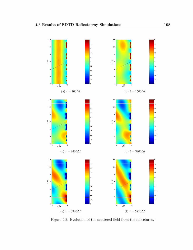
4.3 Results of FDTD Reflectarray Simulations 108
(a) t = 700∆t (b) t = 1500∆t
(c) t = 2420∆t (d) t = 3200∆t
(e) t = 3920∆t (f) t = 5820∆t
Figure 4.3: Evolution of the scattered field from the reflectarray

4.3 Results of FDTD Reflectarray Simulations 109
transient response of the array, this time is very short. Therefore, beam-forming can
occur at a very high rate for this tunable reflectarray platform.
4.3.2 Specular Reflection
Using the same FDTD simulation, and performing the proposed near-to-far-field
transformation of the electric and magnetic fields observed in the aperture shown
in Figure 4.2, the far-field electric field of the array was computed. Far-field values
were normalized to the electric field established in the far field by a perfect plane
wave travelling in the direction (θ = 90, φ = 90) (i.e., the incident wave).
At n = 1, or θ = 63, the reflected energy produced was 0.55 dB below that of
the incident wave, indicating that 93.8% of the incident energy had been re-directed
successfully in the desired direction. This indicates that the array geometry based
on the proposed cell has very high reflection efficiency in the absence of loss.
The remaining energy is scattered in other directions, including the specular
direction. For the sub-array considered, angular harmonics producing real-valued
angles corresponded to n = −2 . . . 2. The normalized angular spectrum of the sub-
array of Figure 4.2 is plotted in Figure 4.4. As observable in the plot, the measured
specular reflection was 41.54 dB below the level of the incident wave, which is very
low. A small amount of reflected energy was also observable at other angles, which
is attributable to phasing error from the elements, introduced when the elements
were assembled into a sub-array. The phasing error also introduced some error in
the specular reflection value, as we will see shortly.
An interesting observation is that not all of the incident energy is accounted
for in the spectrum shown in Figure 4.4. In total, the total power accounted for
4.3 Results of FDTD Reflectarray Simulations 110
-45
-40
-35
-30
-25
-20
-15
-10
-5
0
20 40 60 80 100 120 140 160
Ref
lect
ion
ampl
itude
[dB
]
Elevation angle [deg]
Figure 4.4: Angular spectrum of the simulated sub-array
is only 94.1% of the incident power. The remaining power is likely being lost to
a surface wave mode established at the dielectric-air interface, and travels in the
transverse plane in a non-radiative mode. In an infinite array as simulated, this
energy continues to travel along the substrate surface and is lost. In practise, when
this energy reaches the edge of the substrate in the case of a finite-sized reflectarray,
it is converted to a radiation mode which leads to additional energy being produced
in the broadside direction. However, the contribution of this type of radiation to the
specular reflection was not considered in this analysis.
The alternative method of computing specular reflection, based on superposing
the responses of two oppositely-phased unit cells, was investigated next. The FDTD
parameters of the simulation were similar to those presented in Table 4.1, except
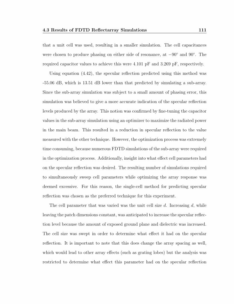
4.3 Results of FDTD Reflectarray Simulations 111
that a unit cell was used, resulting in a smaller simulation. The cell capacitances
were chosen to produce phasing on either side of resonance, at −90 and 90. The
required capacitor values to achieve this were 4.101 pF and 3.269 pF, respectively.
Using equation (4.42), the specular reflection predicted using this method was
-55.06 dB, which is 13.51 dB lower than that predicted by simulating a sub-array.
Since the sub-array simulation was subject to a small amount of phasing error, this
simulation was believed to give a more accurate indication of the specular reflection
levels produced by the array. This notion was confirmed by fine-tuning the capacitor
values in the sub-array simulation using an optimizer to maximize the radiated power
in the main beam. This resulted in a reduction in specular reflection to the value
measured with the other technique. However, the optimization process was extremely
time consuming, because numerous FDTD simulations of the sub-array were required
in the optimization process. Additionally, insight into what effect cell parameters had
on the specular reflection was desired. The resulting number of simulations required
to simultaneously sweep cell parameters while optimizing the array response was
deemed excessive. For this reason, the single-cell method for predicting specular
reflection was chosen as the preferred technique for this experiment.
The cell parameter that was varied was the unit cell size d. Increasing d, while
leaving the patch dimensions constant, was anticipated to increase the specular reflec-
tion level because the amount of exposed ground plane and dielectric was increased.
The cell size was swept in order to determine what effect it had on the specular
reflection. It is important to note that this does change the array spacing as well,
which would lead to other array effects (such as grating lobes) but the analysis was
restricted to determine what effect this parameter had on the specular reflection

4.3 Results of FDTD Reflectarray Simulations 112
performance alone.
The unit cell size was swept from 20 mm to 45 mm in 2.5 mm steps. The required
varactor diode capacitance values to produce phasing at ±90 are summarized in
Table 4.3, which were determined through unit cell scattering simulations.
Cell size d Capacitance for −90 Capacitance for +90
20 mm 0.360 pF 0.185 pF22.5 mm 0.421 pF 0.276 pF25 mm 0.423 pF 0.304 pF27.5 mm 0.417 pF 0.318 pF30 mm 0.410 pF 0.327 pF32.5 mm 0.403 pF 0.332 pF35 mm 0.396 pF 0.335 pF37.5 mm 0.389 pF 0.337 pF40 mm 0.381 pF 0.337 pF42.5 mm 0.374 pF 0.336 pF45 mm 0.368 pF 0.333 pF
Table 4.3: Varactor diode capacitances required to create oppositely-phased unitcells
The results of the specular reflection calculations are illustrated in Figure 4.5.
As expected, the amount of specular reflection increases significantly with cell size.
While the curve does not conform to a perfect line of best fit (likely attributable
to finite-precision effects in the simulation, as well as the fact that the two unit
cell simulations were not exactly 180 out of phase), it is monotonic (except for
the second point, attributable to numerical noise) and demonstrates the expected
behaviour adequately, as we will see in the following discussion.
Below a cell size of 35 mm, the specular reflection is insignificant, lying at least
50 dB below the incident wave amplitude. However, past this point, the specular
reflection increases substantially with cell size. At a cell size of d = 40 mm, the
4.3 Results of FDTD Reflectarray Simulations 113
specular reflection has risen to -25 dB, which is significant because even for a finite
array, this is beginning to exceed the sidelobe levels for a reasonably-sized array. At
the extreme end of the sweep, the specular reflection is only 10 dB below the power
of the incident wave, which accounts for a 10% power loss.
-80
-70
-60
-50
-40
-30
-20
-10
0
20 25 30 35 40 45
Spe
cula
r re
flect
ion
ampl
itude
[dB
]
Cell size (d) [mm]
Figure 4.5: Specular reflection as a function of unit cell size
This interesting behaviour can be explained by examining the effective area of
a microstrip patch antenna. A patch antenna with the parameters presented in
Section 3.3.1 has a theoretical gain of 7 dB or 5.02. According to equation (2.10),
this corresponds to an effective area of 0.0011876 m2, which is just about the same
physical area as a 35 mm unit cell. Hence, when the physical area of the cell is less
than the effective area of the patch, the patch does a very good job of collecting all
the incident energy and re-directing it into the scattered field, producing minimal

4.3 Results of FDTD Reflectarray Simulations 114
specular reflection as shown in Figure 4.5. However, once the cell area exceeds the
effective area of the patch, the patch is incapable of collecting all the energy for
conversion into a scattered field. The remainder of the energy is reflected in the
specular direction, leading to a pronounced increase in this form of loss. This is
an intuitively satisfying result, which directly links the gain of a microstrip patch
antenna into the behaviour of a reflectarray as discussed in Section 4.1. The results
prove that the effective area of a well-designed unit cell, which produces minimal
specular reflection, is equal to the physical area of cell, allowing the gain expression
for reflector antennas to be used to evaluate the gain of reflectarray antennas.

Chapter 5
Experimental Reflectarray Designs
Chapter 3 demonstrated that creating an electronically tunable phase agile re-
flectarray element is indeed possible. Tunability can be added to reflectarray
cells that enables them to be phased over a broad range, which in turn, allows
beam-scanning to be produced from a reflectarray with minimal phase errors in the
aperture. Armed with an accurate technique for evaluating the performance of re-
flectarrays, as presented in Chapter 4, the next step is to design and analyze the
performance of experimental reflectarray prototypes.
This chapter discusses the design of two experimental reflectarrays based on the
cell topology presented in Chapter 3. It begins with an overview of both designs.
Experimental measurement methodology is discussed next. Finally, the bulk of the
chapter focuses on experimental measurements of both prototypes and comparison
with predicted performance.
5.1 Overview of Experimental Reflectarray Designs
Two experimental prototypes were developed for this project. The first was a proof-
of-concept, fixed-beam reflectarray in which fixed capacitors were used in place of
varactor diodes. It was used initially to validate both the performance of the unit cell
and the accuracy of the analysis technique. The second design was an electronically
tunable reflectarray with full electronic control over the reflectarray elements.

5.1 Overview of Experimental Reflectarray Designs 116
The design parameters for both arrays were very similar and are summarized in
Table 5.1. To compute the gain of the individual element designs, equation (4.11)
was evaluated numerically for the patch dimensions shown.
Parameter Fixed Design Electronically Tunable Design
Design frequency f0 5.5 GHz 5.8 GHzSubstrate εr 3.05 3.02Substrate height h 1.524 mm 1.524 mmPatch length L 19 mm 17 mmPatch width W 14 mm 14 mmElement spacing d 30 mm (0.55λ0) 30 mm (0.58λ0)No. of elements in E-plane M 7 7No. of elements in H-plane N 10 10Total dimensions 300 mm × 210 mm 335 mm × 284 mmElement directivity DE 7.00 dB 6.82 dB
Table 5.1: Design parameters of the two experimental reflectarray designs
Both reflectarrays were designed with 70 elements arranged in a 7×10 grid. While
this yielded a reasonably-sized array for experimental purposes, it is generally small
as far as reflectarrays are concerned. The prototypes were intended to represent
sections of a larger reflectarray. 70 elements was chosen as the array size primarily
to keep assembly time, as well as costs, down in the case of the electronically tunable
prototype.
Specific details of the individual designs are given in the following sections. The
coordinate system used for the reflectarray designs and measurements is shown in
Figure 5.1, which shows the reflectarray with θ = 90. θ = 0 defines a reflectarray
lying in the xy-plane.

5.1 Overview of Experimental Reflectarray Designs 117
Figure 5.1: Coordinate system used for reflectarray design and measurements
5.1.1 Fixed Reflectarray Design
The fixed reflectarray was constructed by soldering fixed capacitors in the 0.05-
1.00 pF range in place of the varactor diodes. The bias network and traces were
omitted from the reflectarray cell. The same surface-mount capacitors used in the
experiment of Chapter 3 were used. Since this was a proof-of-concept design, it was
decided that the reflectarray would be designed to reflect a plane wave from one
direction to another, instead of collimating spherical waves from a near-field feed
into a plane wave. This simplifies the design considerably while demonstrating the
beam-forming capability of the reflectarray topology.
The reflectarray’s elements were chosen such that the array would reflect a
plane wave incident from the broadside direction, to the direction of θ = 109 and
φ = −24. This involved using array theory to calculate the phase gradient required
in the array, and discretizing this gradient according to the available capacitor val-
ues. The FDTD PPWG data points in Figure 3.16 were used as a design curve to
map capacitance to scattered field phase, leading to the distribution of the resulting
capacitor values shown in Table 5.2. The actual layout of the reflectarray is shown

5.1 Overview of Experimental Reflectarray Designs 118
in Table 5.3, where the origin is located at the bottom left-hand corner of the table.
Capacitor Pairs required
0.10 pF 20.20 pF 110.30 pF 180.35 pF 210.40 pF 90.50 pF 40.55 pF 10.60 pF 10.70 pF 20.80 pF 00.90 pF 01.00 pF 1
TOTAL 70
Table 5.2: Distribution of capacitor pairs in the fixed reflectarray design
0.30 0.30 0.10 0.40 0.35 0.30 0.20 0.70 0.40 0.350.35 0.30 0.30 1.00 0.40 0.35 0.30 0.20 0.50 0.350.40 0.35 0.30 0.20 0.55 0.35 0.35 0.30 0.20 0.500.70 0.40 0.35 0.30 0.20 0.50 0.35 0.35 0.30 0.200.20 0.60 0.35 0.35 0.30 0.20 0.40 0.35 0.35 0.300.30 0.20 0.50 0.35 0.35 0.30 0.20 0.40 0.35 0.300.35 0.30 0.20 0.40 0.35 0.30 0.30 0.10 0.40 0.35
Table 5.3: Fixed reflectarray design (all capacitor values in pF)
A photo of the completed reflectarray is shown in Figure 5.2. The panel was
mounted in the anechoic chamber and scanned in the far field; hence, no near-field
feed horn is visible. A discussion of the methodology for this type of measurement
is provided in Section 5.2.
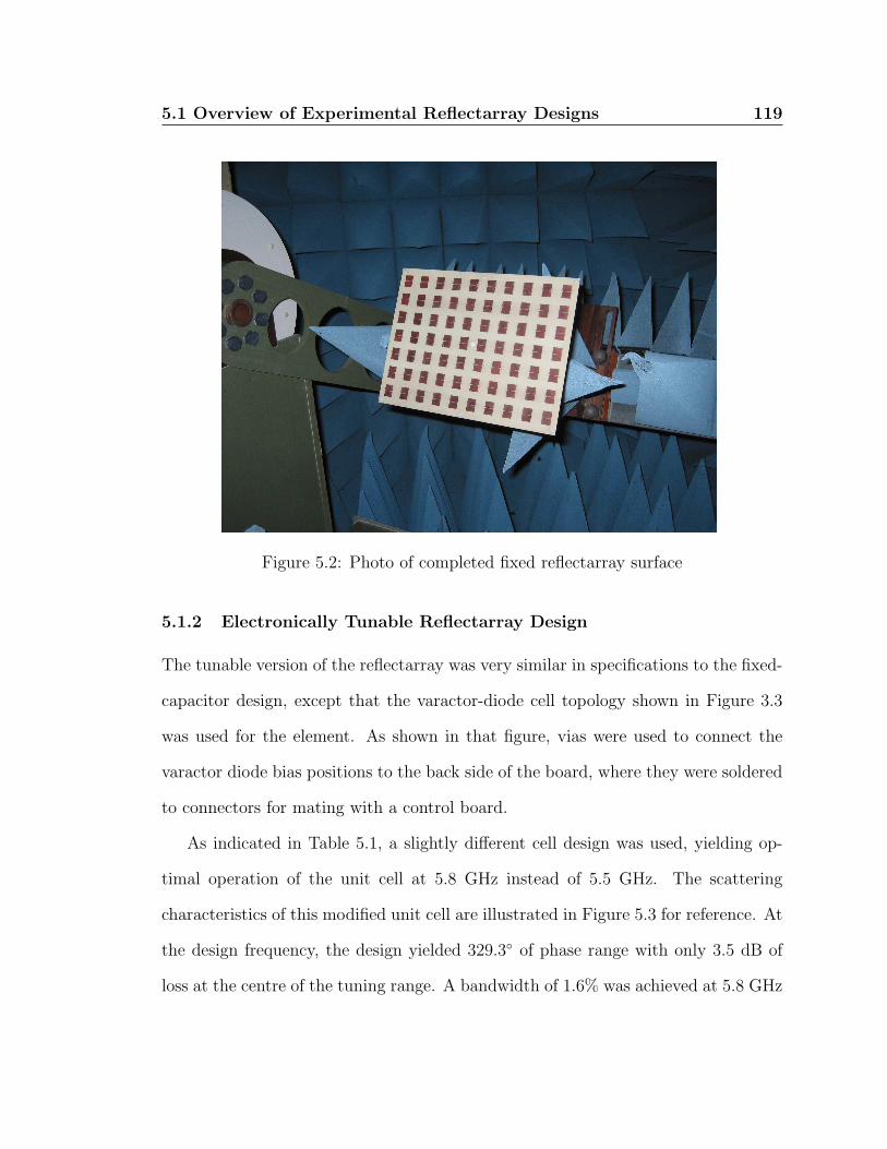
5.1 Overview of Experimental Reflectarray Designs 119
Figure 5.2: Photo of completed fixed reflectarray surface
5.1.2 Electronically Tunable Reflectarray Design
The tunable version of the reflectarray was very similar in specifications to the fixed-
capacitor design, except that the varactor-diode cell topology shown in Figure 3.3
was used for the element. As shown in that figure, vias were used to connect the
varactor diode bias positions to the back side of the board, where they were soldered
to connectors for mating with a control board.
As indicated in Table 5.1, a slightly different cell design was used, yielding op-
timal operation of the unit cell at 5.8 GHz instead of 5.5 GHz. The scattering
characteristics of this modified unit cell are illustrated in Figure 5.3 for reference. At
the design frequency, the design yielded 329.3 of phase range with only 3.5 dB of
loss at the centre of the tuning range. A bandwidth of 1.6% was achieved at 5.8 GHz
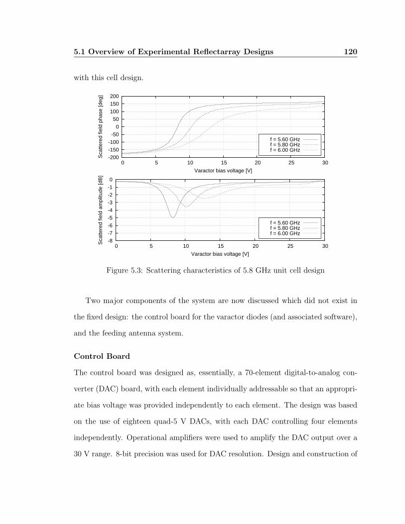
5.1 Overview of Experimental Reflectarray Designs 120
with this cell design.
-8-7-6-5-4-3-2-1 0
0 5 10 15 20 25 30Sca
ttere
d fie
ld a
mpl
itude
[dB
]
Varactor bias voltage [V]
f = 5.60 GHzf = 5.80 GHzf = 6.00 GHz
-200-150-100-50
0 50
100 150 200
0 5 10 15 20 25 30
Sca
ttere
d fie
ld p
hase
[deg
]
Varactor bias voltage [V]
f = 5.60 GHzf = 5.80 GHzf = 6.00 GHz
Figure 5.3: Scattering characteristics of 5.8 GHz unit cell design
Two major components of the system are now discussed which did not exist in
the fixed design: the control board for the varactor diodes (and associated software),
and the feeding antenna system.
Control Board
The control board was designed as, essentially, a 70-element digital-to-analog con-
verter (DAC) board, with each element individually addressable so that an appropri-
ate bias voltage was provided independently to each element. The design was based
on the use of eighteen quad-5 V DACs, with each DAC controlling four elements
independently. Operational amplifiers were used to amplify the DAC output over a
30 V range. 8-bit precision was used for DAC resolution. Design and construction of
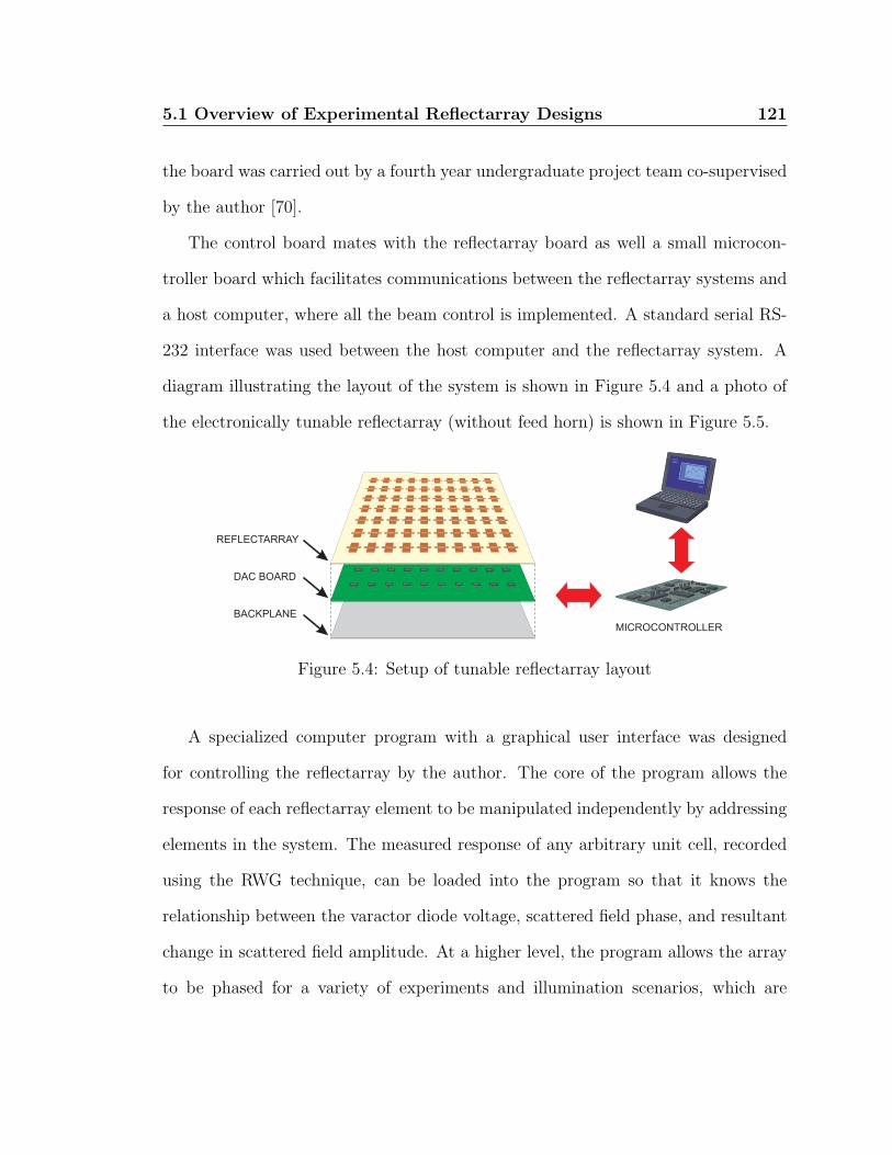
5.1 Overview of Experimental Reflectarray Designs 121
the board was carried out by a fourth year undergraduate project team co-supervised
by the author [70].
The control board mates with the reflectarray board as well a small microcon-
troller board which facilitates communications between the reflectarray systems and
a host computer, where all the beam control is implemented. A standard serial RS-
232 interface was used between the host computer and the reflectarray system. A
diagram illustrating the layout of the system is shown in Figure 5.4 and a photo of
the electronically tunable reflectarray (without feed horn) is shown in Figure 5.5.
Figure 5.4: Setup of tunable reflectarray layout
A specialized computer program with a graphical user interface was designed
for controlling the reflectarray by the author. The core of the program allows the
response of each reflectarray element to be manipulated independently by addressing
elements in the system. The measured response of any arbitrary unit cell, recorded
using the RWG technique, can be loaded into the program so that it knows the
relationship between the varactor diode voltage, scattered field phase, and resultant
change in scattered field amplitude. At a higher level, the program allows the array
to be phased for a variety of experiments and illumination scenarios, which are
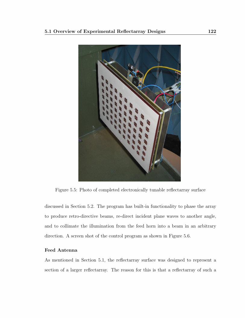
5.1 Overview of Experimental Reflectarray Designs 122
Figure 5.5: Photo of completed electronically tunable reflectarray surface
discussed in Section 5.2. The program has built-in functionality to phase the array
to produce retro-directive beams, re-direct incident plane waves to another angle,
and to collimate the illumination from the feed horn into a beam in an arbitrary
direction. A screen shot of the control program as shown in Figure 5.6.
Feed Antenna
As mentioned in Section 5.1, the reflectarray surface was designed to represent a
section of a larger reflectarray. The reason for this is that a reflectarray of such a
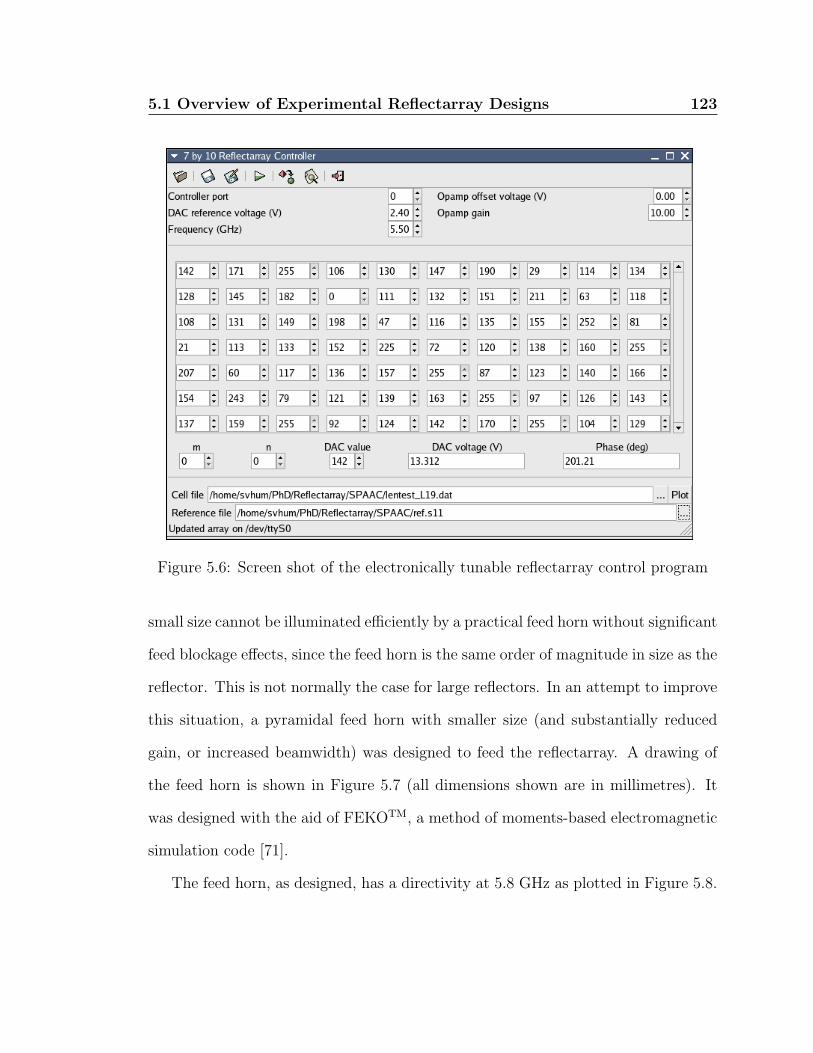
5.1 Overview of Experimental Reflectarray Designs 123
Figure 5.6: Screen shot of the electronically tunable reflectarray control program
small size cannot be illuminated efficiently by a practical feed horn without significant
feed blockage effects, since the feed horn is the same order of magnitude in size as the
reflector. This is not normally the case for large reflectors. In an attempt to improve
this situation, a pyramidal feed horn with smaller size (and substantially reduced
gain, or increased beamwidth) was designed to feed the reflectarray. A drawing of
the feed horn is shown in Figure 5.7 (all dimensions shown are in millimetres). It
was designed with the aid of FEKOTM, a method of moments-based electromagnetic
simulation code [71].
The feed horn, as designed, has a directivity at 5.8 GHz as plotted in Figure 5.8.
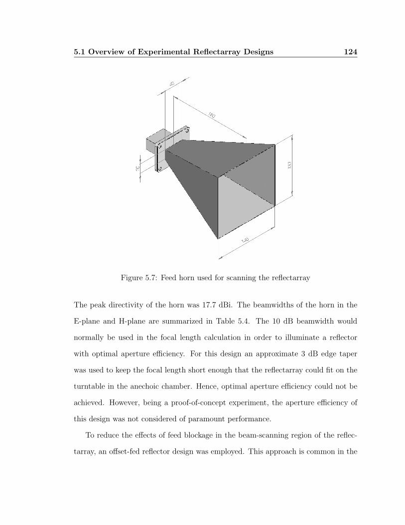
5.1 Overview of Experimental Reflectarray Designs 124
Figure 5.7: Feed horn used for scanning the reflectarray
The peak directivity of the horn was 17.7 dBi. The beamwidths of the horn in the
E-plane and H-plane are summarized in Table 5.4. The 10 dB beamwidth would
normally be used in the focal length calculation in order to illuminate a reflector
with optimal aperture efficiency. For this design an approximate 3 dB edge taper
was used to keep the focal length short enough that the reflectarray could fit on the
turntable in the anechoic chamber. Hence, optimal aperture efficiency could not be
achieved. However, being a proof-of-concept experiment, the aperture efficiency of
this design was not considered of paramount performance.
To reduce the effects of feed blockage in the beam-scanning region of the reflec-
tarray, an offset-fed reflector design was employed. This approach is common in the
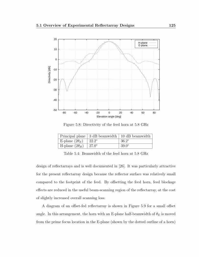
5.1 Overview of Experimental Reflectarray Designs 125
-50
-40
-30
-20
-10
0
10
20
-80 -60 -40 -20 0 20 40 60 80
Dire
ctiv
ity [d
Bi]
Elevation angle [deg]
H-planeE-plane
Figure 5.8: Directivity of the feed horn at 5.8 GHz
Principal plane 3 dB beamwidth 10 dB beamwidthE-plane (2θE) 22.2 36.2
H-plane (2θH) 27.0 39.0
Table 5.4: Beamwidth of the feed horn at 5.8 GHz
design of reflectarrays and is well documented in [26]. It was particularly attractive
for the present reflectarray design because the reflector surface was relatively small
compared to the footprint of the feed. By offsetting the feed horn, feed blockage
effects are reduced in the useful beam-scanning region of the reflectarray, at the cost
of slightly increased overall scanning loss.
A diagram of an offset-fed reflectarray is shown in Figure 5.9 for a small offset
angle. In this arrangement, the horn with an E-plane half-beamwidth of θE is moved
from the prime focus location in the E-plane (shown by the dotted outline of a horn)

5.1 Overview of Experimental Reflectarray Designs 126
in a circular arc to an offset location. The change in illumination angle is denoted θi.
The reflectarray can also be offset in the x-direction if desired. A constant distance
Ri = F is maintained between the centre of the reflectarray and the feed horn, where
F is the focal length of the reflectarray with a prime-focus feed. Offsetting the feed
horn in this way displaces it by distances Xf and Zf in Cartesian coordinates.
Figure 5.9: Offset feed geometry for a reflectarray
For this design, a prime focus feed with a 3 dB edge taper in the H-plane resulted
in a focal length of
F =D
2 tan θE= 0.5161 m (5.1)
where D = Md = 210 mm was used. The illumination angle θi was selected as
20. This produced a reasonably large visible region in front of the reflectarray while
offsetting the feed horn well below the axis of the reflectarray, reducing feed blockage.
Offsetting the horn in this manner required the horn to be offset such that
Zf = Ri cos θi = 489.6 mm (5.2)

5.2 Measurement Methodology 127
and
Xf = Ri sin θi = 178.2 mm. (5.3)
This resulted in a total subtended aperture in the E-plane of the reflectarray of
208.5 mm, which is close to the height of the reflectarray panel. The subtended
aperture in the H-plane is 222.5 mm wide, which is only slightly less than its length
of 300 mm. The effect of this is a slight reduction in taper efficiency.
A plot of the illumination pattern on the un-subtended aperture is shown in
Figure 5.10, where the contours are in dB. The 3 dB edge-taper in the E-plane is
clearly visible, as well as illumination asymmetry in the E-plane due to the offsetting
of the feed. The anticipated spillover and taper efficiencies were computed from this
illumination pattern, and are summarized in Table 5.5. Considering only feed effects,
the resulting aperture efficiency of 42.8% was deemed to be quite good considering
the short focal length required for practical measurements of the reflectarray.
Efficiency Calculated valueSpillover efficiency (εs) 53.6%Illumination taper efficiency (εt) 80.0%
Aperture efficiency (εsεt) 42.8%
Table 5.5: Aperture efficiencies and sub-efficiencies of the offset feed
5.2 Measurement Methodology
To study the performance of the reflectarray designs, experiments were conducted
in an anechoic chamber. The system in this chamber allows antennas under test to
be mounted on a turntable and positioner, allowing the response of antenna to be
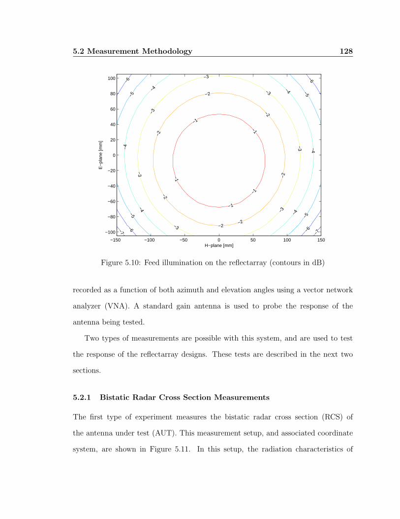
5.2 Measurement Methodology 128
−7
−7 −6
−6
−6−6
−5
−5
−5−5
−4
−4
−4
−4
−4
−4
−3
−3
−3
−3
−3
−3
−3−2
−2
−2
−2
−2
−2
−2
−1
−1
−1
−1
−1
H−plane [mm]
E−
plan
e [m
m]
−150 −100 −50 0 50 100 150
−100
−80
−60
−40
−20
0
20
40
60
80
100
Figure 5.10: Feed illumination on the reflectarray (contours in dB)
recorded as a function of both azimuth and elevation angles using a vector network
analyzer (VNA). A standard gain antenna is used to probe the response of the
antenna being tested.
Two types of measurements are possible with this system, and are used to test
the response of the reflectarray designs. These tests are described in the next two
sections.
5.2.1 Bistatic Radar Cross Section Measurements
The first type of experiment measures the bistatic radar cross section (RCS) of
the antenna under test (AUT). This measurement setup, and associated coordinate
system, are shown in Figure 5.11. In this setup, the radiation characteristics of
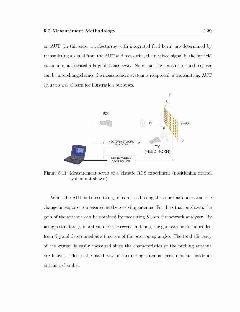
5.2 Measurement Methodology 129
an AUT (in this case, a reflectarray with integrated feed horn) are determined by
transmitting a signal from the AUT and measuring the received signal in the far field
at an antenna located a large distance away. Note that the transmitter and receiver
can be interchanged since the measurement system is reciprocal; a transmitting AUT
scenario was chosen for illustration purposes.
Figure 5.11: Measurement setup of a bistatic RCS experiment (positioning controlsystem not shown)
While the AUT is transmitting, it is rotated along the coordinate axes and the
change in response is measured at the receiving antenna. For the situation shown, the
gain of the antenna can be obtained by measuring S12 on the network analyzer. By
using a standard gain antenna for the receive antenna, the gain can be de-embedded
from S12 and determined as a function of the positioning angles. The total efficiency
of the system is easily measured since the characteristics of the probing antenna
are known. This is the usual way of conducting antenna measurements inside an
anechoic chamber.

5.2 Measurement Methodology 130
The ideal bistatic RCS of a reflectarray is defined as its gain response evaluated
at the desired beam pointing angle (θb, φb). It can be written as
RCSb(θb, φb) = Ge(θb, φb) cos θb
N−1∑
n=0
M−1∑
m=0
Amn(θmn, φmn, ψmn)
ejk0(x′
mn sin θb cosφb+y′
mn sin θb sinφb)ejψmn (5.4)
where: Ge(θb, φb) is the gain of the reflectarray element at the beam pointing an-
gle and (θmn, φmn) is the feed illumination angle to the mnth element. The cos θ
term appears in front of the summation to account for the apparent reduction in
reflectarray cross section as it is scanned off broadside.
5.2.2 Monostatic Radar Cross Section Measurements
An alternative method of measuring the response of an antenna is to measure its
monostatic RCS. In this setup, the radiation characteristics of the AUT are measured
at the same point in space. That is, a signal is transmitted from the probing antenna
to the AUT, where it is scattered, and then received by the exact same probing
antenna. By rotating the AUT along the coordinate axes, the amount of reflection
produced by the AUT can be measured. The monostatic RCS measurement setup for
a reflectarray is shown in Figure 5.12. By measuring S11 in this setup, the reflectivity
of the reflectarray surface can be characterized.
This is not the normal way in which reflectarrays are scanned, since the feed
horn that normally excites the reflectarray is removed and just the reflector sur-
face is measured. However, this method has a number of advantages for measuring
reflectarray antennas in particular. First, it is an excellent way to characterize the
efficiency of the reflector surface without having to deal with illumination effects such
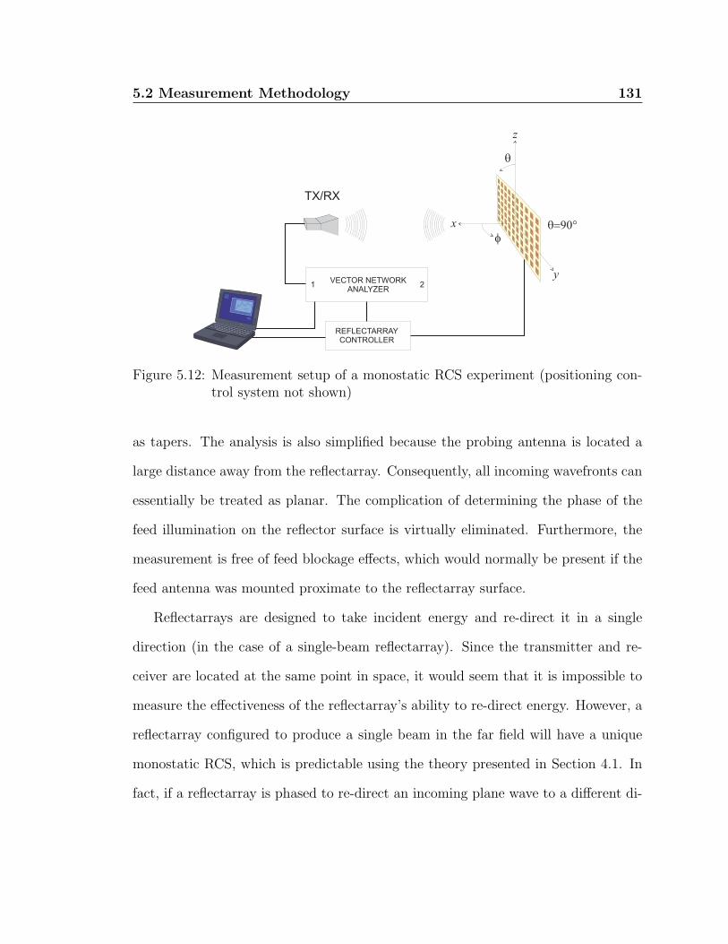
5.2 Measurement Methodology 131
Figure 5.12: Measurement setup of a monostatic RCS experiment (positioning con-trol system not shown)
as tapers. The analysis is also simplified because the probing antenna is located a
large distance away from the reflectarray. Consequently, all incoming wavefronts can
essentially be treated as planar. The complication of determining the phase of the
feed illumination on the reflector surface is virtually eliminated. Furthermore, the
measurement is free of feed blockage effects, which would normally be present if the
feed antenna was mounted proximate to the reflectarray surface.
Reflectarrays are designed to take incident energy and re-direct it in a single
direction (in the case of a single-beam reflectarray). Since the transmitter and re-
ceiver are located at the same point in space, it would seem that it is impossible to
measure the effectiveness of the reflectarray’s ability to re-direct energy. However, a
reflectarray configured to produce a single beam in the far field will have a unique
monostatic RCS, which is predictable using the theory presented in Section 4.1. In
fact, if a reflectarray is phased to re-direct an incoming plane wave to a different di-

5.2 Measurement Methodology 132
rection, there are several angles where retro-directive beams exist. That is, there are
illumination angles where the reflectarray surface reflects the entire incoming plane
wave in the same direction. This behaviour is very predictable, and serves as a useful
way of quantifying the performance of the array. The un-normalized reflectivity of a
reflectarray surface can can be computed theoretically using equation (4.7) subject
to a transmit and receive process at the same physical location in space:
R(θ, φ) = G2e(θ, φ)
N−1∑
n=0
M−1∑
m=0
Amn(θmn, φmn, ψmn)
ej2k0(x′mn sin θ cosφ+y′mn sin θ sinφ)ejψmn . (5.5)
It is observed the element gain has been squared because scanning loss affects both
the incoming and outgoing waves. For the same reason, the first complex exponen-
tial appearing in equation (4.7) is squared because phase delay introduced by the
incoming wave manifests itself in the phases of the waves departing the reflectarray.
To understand the retro-directive behaviour of a reflectarray, consider the situ-
ation shown in Figure 5.13, which shows an ideal model of a one-dimensional re-
flectarray. Incoming waves are received by antenna elements, which phase shift the
incoming signal by ψn before rebroadcasting it.
Assume that the reflectarray is configured to re-direct a plane wave at broadside
to some other direction. From equation (2.20), the required inter-element phase shift
to form a beam at an angle θ0 from the z-axis is α = k0d cos θ0. Assume that the
reflectarray has been programmed with this inter-element phase shift so that the
described plane wave re-direction is achieved. That is,
∆ψ = ψn+1 − ψn = k0d cos θ0. (5.6)
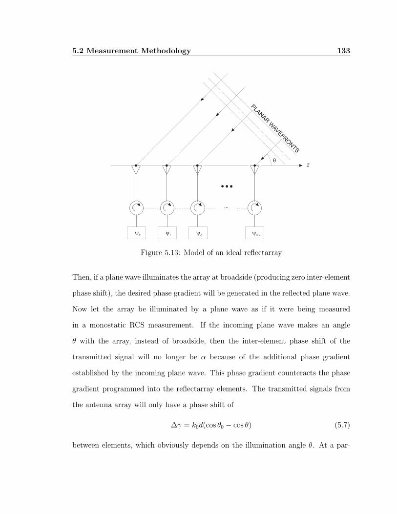
5.2 Measurement Methodology 133
Figure 5.13: Model of an ideal reflectarray
Then, if a plane wave illuminates the array at broadside (producing zero inter-element
phase shift), the desired phase gradient will be generated in the reflected plane wave.
Now let the array be illuminated by a plane wave as if it were being measured
in a monostatic RCS measurement. If the incoming plane wave makes an angle
θ with the array, instead of broadside, then the inter-element phase shift of the
transmitted signal will no longer be α because of the additional phase gradient
established by the incoming plane wave. This phase gradient counteracts the phase
gradient programmed into the reflectarray elements. The transmitted signals from
the antenna array will only have a phase shift of
∆γ = k0d(cos θ0 − cos θ) (5.7)
between elements, which obviously depends on the illumination angle θ. At a par-

5.2 Measurement Methodology 134
ticular angle, θr, all element signals will add coherently and a beam will be formed
in that direction. This angle is found by setting equation (5.7) to zero, resulting in
θr = cos−1
(
cos θ0
2
)
(5.8)
which is the direction of the retro-directive beam formed by the reflectarray.
In a monostatic RCS experiment, the reflectarray is programmed to re-direct a
plane wave at broadside to another angle. The reflectivity of the array surface can
be measured and compared to that predicted by array theory. If the array is working
properly, there should be a good correlation between the theoretical reflectivity of
the reflectarray, described by equation (5.5), and the measurement, including the
location and amplitude of the retro-directive beam. For a 2-D reflectarray based on
microstrip patch elements, under some circumstances two retro-directive beams will
be visible because of the existence of multiple solutions to equation (5.8).
The monostatic RCS is defined as the reflectivity of the reflectarray surface eval-
uated at the retro-directive beam pointing angle (θr, φr) produced by the array. It
is defined as
RCSm(θr, φr) = G2e(θr, φr) cos2 θr
N−1∑
n=0
M−1∑
m=0
Amn(θmn, φmn, ψmn)
ej2k0(x′mn sin θr cosφr+y′mn sin θr sinφr)ejψmn (5.9)
As with the bistatic RCS case, a cos θ term has been introduced to account for the
change in cross section of the reflectarray as it is scanned. For the same reason the
gain terms were squared in equation (5.5), the cos θ term is squared here.

5.2 Measurement Methodology 135
5.2.3 Description of Experiments
Two measurement methods have been described for quantifying the performance of
reflectarrays. Ultimately, a bistatic RCS measurement is important to demonstrate
the performance of the reflectarray in its natural configuration. The monostatic RCS
measurement, however, is extremely useful for preliminary testing of the reflectar-
ray surface because, as mentioned, feed blockage is not a concern and plane wave
assumptions can be used to simplify the reflectarray synthesis and analysis.
The fixed reflectarray design, which was designed early in the research program,
was a proof-of-concept design. It was characterized using a monostatic RCS measure-
ment using the technique described in the previous section. It was “programmed”
to re-direct a plane wave incident at broadside to a certain outgoing angle. The
reflector surface was characterized in the far field and the reflectivity of the surface
measured as a function of scan angle to confirm that retro-directive beams, and the
rest of the reflectivity pattern, behaved as expected by array theory. The monostatic
RCS is used to verify the expected loss in the retro-directive beam. This experiment
is described in Section 5.3.
The electronically tunable reflectarray design was characterized using both meth-
ods. Initially, it was tested using a monostatic measurement, because the reflector
efficiency of the surface could be quantified without having to worry about feed ef-
fects (e.g., taper efficiency, spillover loss, etc.) Once the reflective properties of the
tunable surface were measured, a bistatic measurement was performed whereby the
reflectarray was scanned in its normal configuration with a proximal feed horn.
Experiments with the tunable reflectarray were also considered with and without

5.2 Measurement Methodology 136
the use of a closed-loop controller. By default, the array controller uses open-loop
control whereby a single cell measurement, such as that shown in Figure 5.3, forms
the basis for a lookup table for mapping desired phases values to appropriate varactor
bias voltages. Such a control scheme can lead to aperture phase errors if there is
significant variance in the phase characteristic from element to element, such that the
lookup table is no longer sufficiently accurate to phase the array without a significant
reduction in reflector efficiency. This problem can be potentially quite pronounced
for an electronically tunable reflectarray for a number of reasons:
1. The manufactured patch dimensions from cell to cell can vary significantly,
leading to departures in the phase response from the curve used by the array
controller (Figure 5.3). Analysis of the accuracy of the technology used to
manufacture the array (a printed circuit board milling machine), reveals that
up to a ±2.4% variation in patch dimensions is possible. However, this is
not anticipated to be a major source of phase error in this case. The same
technology was used to manufacture the fixed-capacitor reflectarray, where
the dimensions of the patches were consistent with design values, and severe
phase errors (after phase discretization and range was accounted for), were not
observed (as will be discussed in Section 5.3).
2. The varactor diode parameters could vary significantly from diode to diode.
The cell’s response could also be impacted if two diodes with widely different
characteristics were paired together in a cell. According to the manufacturer,
up to a ±11% variation in varactor diode junction capacitance was possible
from the lot of diodes used [65], which is a significant variation. To compound

5.2 Measurement Methodology 137
this problem, varactor diode capacitance is a fairly strong function of temper-
ature which can also produce departures from the design curve.
3. There is a slight but known deviation between the phasing characteristic mea-
sured in a rectangular waveguide and an actual cell because of the short height
of the waveguide used in the measurement, as shown in Figure 3.16. The fixed-
capacitor design did not suffer from this effect because the FDTD results could
be used as design curves as the capacitor values were known; de-embedding the
actual capacitance of the varactor diode as a function of voltage was difficult
experimentally and hence RWG results had to be used as the design curve.
With a closed-loop control system, which employs physical feedback from the
array, phase error losses can be potentially alleviated. The discussion of such a
controller is presented in the next section.
5.2.4 Self-Phasing Control of Reflectarrays
One of the most interesting features of the tunable reflectarray architecture is that
it is highly amenable to closed-loop control techniques that directly manipulate the
RF signal from each antenna element. Such a system is illustrated in Figure 5.14. In
this setup, demonstrated in receive mode, the power measured at the feed horn can
be used as an optimization metric in a controller and used to manipulate the bias
across the varactor diodes used in each antenna element. Implementing a controller
in this way provides it with a unique capability in receive mode known as self-
phasing. Under this type of control, the array elements are phased such that the
scattered signal from each and every antenna element arrives in phase at the feed
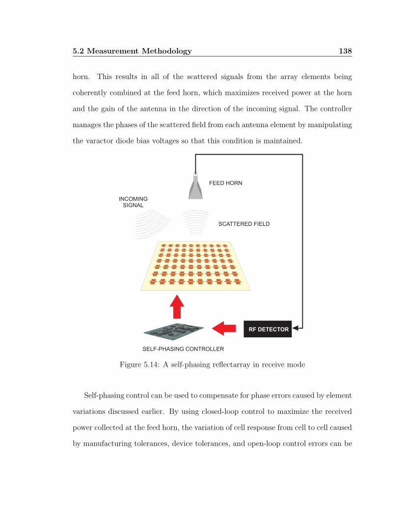
5.2 Measurement Methodology 138
horn. This results in all of the scattered signals from the array elements being
coherently combined at the feed horn, which maximizes received power at the horn
and the gain of the antenna in the direction of the incoming signal. The controller
manages the phases of the scattered field from each antenna element by manipulating
the varactor diode bias voltages so that this condition is maintained.
Figure 5.14: A self-phasing reflectarray in receive mode
Self-phasing control can be used to compensate for phase errors caused by element
variations discussed earlier. By using closed-loop control to maximize the received
power collected at the feed horn, the variation of cell response from cell to cell caused
by manufacturing tolerances, device tolerances, and open-loop control errors can be
5.2 Measurement Methodology 139
effectively dealt with.
Self-phasing control was implemented directly in the experimental setups dis-
cussed in Sections 5.2.2 and 5.2.1, for both the monostatic and bistatic tests. Since
a network analyzer essentially acts as a tuned transceiver, the measured RCS could
be used as an optimization metric. The same computer used to download configura-
tions to the reflectarray controller was also used to communicate with the VNA over
a general purpose instrumentation bus (GPIB). Functions for measuring the fitness
function, or RCS from the instrument, were written into the reflectarray control soft-
ware described in Section 5.1.2. A function call to evaluate the fitness of a particular
array configuration simply entails triggering a sweep on the VNA and querying it
for a measurement.
It is worth noting that since the fitness function for the optimizer is a physi-
cally measured quantity, there is the potential for very fast adaptation, as the fitness
function can be evaluated quickly. In fact, a time for the fitness of a single array con-
figuration to be evaluated is primarily limited by the acquisition time of the network
analyzer, since updating the array is a very fast process (as shown in Section 4.3.1),
even when the communication speed with the array and DAC response time is taken
into account.
For implementing the self-phasing control algorithm, a genetic algorithm (GA)
was chosen. Evolutionary algorithms such as GAs have been successfully employed
in many electromagnetics optimization problems [72] as they are very effective global
optimizers [73]. They have been particularly attractive in the design of antennas and
antenna arrays, where multiple generations of antenna configurations are evolved to
produce a fixed antenna design with desired characteristics. For antenna arrays, GAs
5.2 Measurement Methodology 140
have been used primarily in synthesis problems where the desired radiation pattern is
already known. This work differs considerably in that the pattern is unknown. The
GA is being used to evolve adaptive hardware to optimize reception of a signal of
unknown direction, and respond to changes in the environment or the antenna itself.
There has been some work in using GAs to optimize received signal strength from
reconfigurable antennas based on switches [74][75], and also to minimize interference
by manipulating reconfigurable shape-alloy antennas [76]. Conceivably, they could
be easily adapted to reflectarray control as well.
For the reflectarray problem, GAs appear attractive because optimization inputs
(the varactor bias voltages for each antenna element) can be mapped directly to genes
in a chromosome, and since the varactor voltages are quantized, standard bitwise ge-
netic operators can be used on the chromosomes. The “optimization-over-hardware”
approach enables the optimal antenna configuration to be found in a short period
of time, despite the large problem space which may require the evaluation of many
array configurations. While the technique is not the most efficient of optimizers in
terms of total iterations, speed was not the goal of this experiment; rather, proving
that phase errors could be compensated by using closed-loop control was the funda-
mental goal. Given the large search space and the nonlinear relationship between
the system’s inputs and the output signal, GAs appeared very attractive for this
problem.
The GA was implemented in the reflectarray control software. Details of the
implementation of the GA can be found in Appendix A. The optimization metric
could be selected as either |S11(f = f0)|, or |S12(f = f0)|, depending on whether the
monostatic or bistatic RCS of the reflectarray was being maximized. f0 refers to the

5.3 Fixed Reflectarray Results 141
design frequency of the reflectarray, which was 5.8 GHz for the electronically tunable
reflectarray.
5.3 Fixed Reflectarray Results
For this experiment, the reflectarray surface was placed in the anechoic chamber
and scanned with a standard gain horn located at the far end of the chamber. The
maximum reflectivity was found at θ = 100.5, φ = −12.0, where the antenna acted
as a retro-directive reflector. This compares favourably with the expected values of
θ = 99.0, φ = −10.5. Plots of the measured and theoretical reflectivity for two
different scans of the array are shown in Figures 5.15 and 5.16.
-60
-50
-40
-30
-20
-10
0
-60 -40 -20 0 20 40 60
Arr
ay r
espo
nse
[dB
]
Azimuth angle [deg]
Ideal phasesDiscrete phases
With lossMeasured
Figure 5.15: Measured and simulated monostatic RCS of the fixed reflectarray, θ =100.5
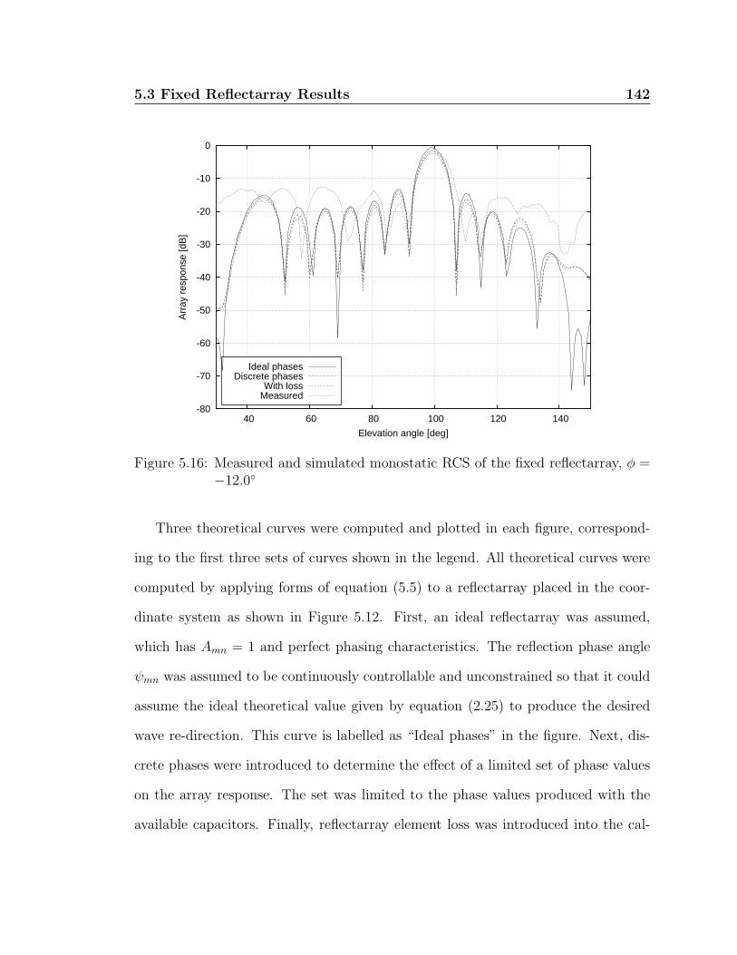
5.3 Fixed Reflectarray Results 142
-80
-70
-60
-50
-40
-30
-20
-10
0
40 60 80 100 120 140
Arr
ay r
espo
nse
[dB
]
Elevation angle [deg]
Ideal phasesDiscrete phases
With lossMeasured
Figure 5.16: Measured and simulated monostatic RCS of the fixed reflectarray, φ =−12.0
Three theoretical curves were computed and plotted in each figure, correspond-
ing to the first three sets of curves shown in the legend. All theoretical curves were
computed by applying forms of equation (5.5) to a reflectarray placed in the coor-
dinate system as shown in Figure 5.12. First, an ideal reflectarray was assumed,
which has Amn = 1 and perfect phasing characteristics. The reflection phase angle
ψmn was assumed to be continuously controllable and unconstrained so that it could
assume the ideal theoretical value given by equation (2.25) to produce the desired
wave re-direction. This curve is labelled as “Ideal phases” in the figure. Next, dis-
crete phases were introduced to determine the effect of a limited set of phase values
on the array response. The set was limited to the phase values produced with the
available capacitors. Finally, reflectarray element loss was introduced into the cal-

5.3 Fixed Reflectarray Results 143
culation to determine its effect. All theoretical curves are normalized to account for
element factor and scanning loss from the array, and hence do not reach 0 dB since
the retro-directive beam lies off broadside.
Before comparing these curves to the measured response, it is worthwhile to
compare them on their own to determine the effects of various reflectarray effects.
First, the monostatic RCS is examined, because ultimately the reflection behaviour
at the retro-direction angle, in the absence of scanning loss, represents the reflection
efficiency of the reflectarray surface as a whole. Comparing the three theoretical
monostatic radar cross section estimates, there are a few important observations.
Discretizing the available phases introduces potentially large phase errors into the
reflectarray surface because only 12 capacitor values are available, and the total phase
range of the reflectarray elements is limited to approximately 335 as discussed in
Section 3.4. The effect of this is to reduce the monostatic RCS, or equivalently, the
reflection efficiency of the surface, by 0.94 dB. Introducing loss in the reflectarray
elements, as shown in the lower subplot of Figure 3.16, reduces the RCS by a further
0.75 dB, yielding a total of 1.7 dB reduction in monostatic RCS. The reduction in
RCS due to loss effects can also be predicted using
∆RCS =
∣
∣
∣
∑N−1n=0
∑M−1m=0 Amn(ψmn)
∣
∣
∣
2
(MN)2(5.10)
In total, phase errors and loss effects have reduced the reflection efficiency of the
ideal reflectarray by 32%, which is significant.
Next, consider the effect of discrete phasing and loss on the overall reflectivity
behaviour. The most significant observation is that phase errors in the discretely-
phased reflectarrays affect sidelobe levels, since scattered combines coherently in

5.3 Fixed Reflectarray Results 144
different locations and at different levels when phase errors are introduced into the
surface. Element loss does not significantly affect the reflectivity behaviour at angles
other than the retro-direction angles.
The measured curves in Figures 5.15 and 5.16 are normalized to the measured
RCS of a metal plate having identical dimensions to the reflectarray panel. In the
far field, and ignoring reflections produced by diffraction, the plate should act close
to an ideal reflector. Hence, the reflection produced by this metal plate represents
the maximum reflected power that could be produced by the reflectarray in the
absence of other losses. Measurements of the monostatic RCS confirmed that at the
retro-direction angle, there was about 1 dB of loss excluding scanning loss. Hence,
the reflection efficiency of the fixed reflector surface is estimated at approximately
80%. Of course, in a real reflectarray implementation, feed effects must be considered
which would substantially reduce the overall reflector efficiency. Nevertheless, the
figure is useful in characterizing the performance of the reflector surface itself.
The overall correlation between the simulated and measured results is very good.
It is expected that the measured curve should most closely resemble the third theo-
retical curve, since this is the most realistic representation of a practical reflectarray.
Discrepancies between theory and measurement, most apparent in the elevation scan,
were likely caused by reflections of a large boom that was used to support the an-
tenna. The boom’s cross-section changed most significantly during elevation angle
scans, leading to large errors when the array was scanned more than 30 from broad-
side. Some beam-pointing error between theoretical and measured results is also
apparent in the elevation scan, which is also not surprising considering that only 7
elements with discrete phasing were used in the H-plane of the array, impacting its

5.4 Electronically Tunable Reflectarray Results 145
ability to accurately point a beam in this principal plane.
The success of this experiment confirmed that the reflectarray cell concept based
on variable capacitors could work in an array scenario. With the demonstrated suc-
cess of this system, the focus of experiments shifted to characterizing the performance
of the electronically tunable system, described in the next section.
5.4 Electronically Tunable Reflectarray Results
As discussed in Section 5.2.3, both monostatic and bistatic RCS measurement ex-
periments were conducted with the electronically tunable reflectarray. Monostatic
RCS performance was considered first, to establish the overall reflection efficiency of
the system without considering feed efficiency. Next, the reflectarray feed horn was
added to analyze the performance of the reflectarray system as a whole in its native
form.
5.4.1 Monostatic RCS Experiment with Open-Loop Control
Initially, for the same reasons the monostatic RCS measurement was used for the
fixed reflectarray, it was used for the electronically tunable reflectarray as well. To
demonstrate the beam-forming functionality of the electronically tunable reflectarray
surface, the array was programmed to form retro-directive beams for a variety of
azimuth angles at a fixed elevation angle of θ = 80. Knowing the desired retro-
direction angle φr, it is a straightforward matter to determine the required element
phasing using array theory since the incident wave is a plane wave originating from
the probe antenna in the far-field. The required phasing of the elements can be

5.4 Electronically Tunable Reflectarray Results 146
determined from equation (5.9) as
ψmn = −2k0(x′mn sin θr cosφr + y′mn sin θr sinφr) (5.11)
where (θr, φr) is the desired retro-directive angle.
For the first experiment, open-loop control was used. Calculations of the re-
quired phasing of the array to produce retro-directive beams were carried out auto-
matically by the control program so that the user could simply supply the desired
retro-directive beam direction, and the required voltages determined from the lookup
table.
Using this control technique, the reflectarray surface was programmed to produce
retro-directive beams at φ = 10, φ = 20, φ = 30, and φ = 40. The results of the
reflectivity measurements for each of these configurations is shown in Figure 5.17.
The desired retro-directive beams are visible on the right side of the plot; the beams
on the left are also expected by array theory, as explained earlier, but are not of
interest.
Overall, the beam positions correlated well with the desired beam angle. Some
beam pointing error at angles far from broadside is apparent and expected due to
the open-loop control scheme used to phase the array. The increased scan loss away
from broadside is also expected and a curve illustrating the expected scan loss is
included in the plot. This loss results from the response of microstrip elements as
well as from the decrease in projected aperture area as the beam is scanned. The
monostatic RCS values from the various configurations correlate well with this curve.
The reflectivity values in Figure 5.17, including the scanning loss curve, have
been normalized with respect the peak RCS measured from a metal plate just as in
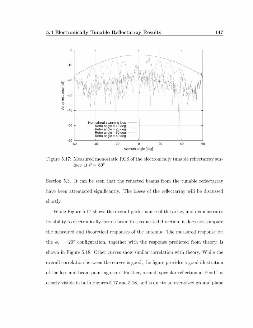
5.4 Electronically Tunable Reflectarray Results 147
-60
-50
-40
-30
-20
-10
0
-60 -40 -20 0 20 40 60
Arr
ay r
espo
nse
[dB
]
Azimuth angle [deg]
Normalized scanning lossRetro angle = 10 degRetro angle = 20 degRetro angle = 30 degRetro angle = 40 deg
Figure 5.17: Measured monostatic RCS of the electronically tunable reflectarray sur-face at θ = 80
Section 5.3. It can be seen that the reflected beams from the tunable reflectarray
have been attenuated significantly. The losses of the reflectarray will be discussed
shortly.
While Figure 5.17 shows the overall performance of the array, and demonstrates
its ability to electronically form a beam in a requested direction, it does not compare
the measured and theoretical responses of the antenna. The measured response for
the φr = 20 configuration, together with the response predicted from theory, is
shown in Figure 5.18. Other curves show similar correlation with theory. While the
overall correlation between the curves is good, the figure provides a good illustration
of the loss and beam-pointing error. Further, a small specular reflection at φ = 0 is
clearly visible in both Figures 5.17 and 5.18, and is due to an over-sized ground plane
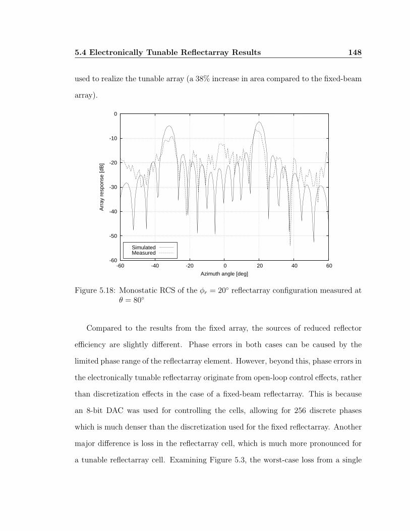
5.4 Electronically Tunable Reflectarray Results 148
used to realize the tunable array (a 38% increase in area compared to the fixed-beam
array).
-60
-50
-40
-30
-20
-10
0
-60 -40 -20 0 20 40 60
Arr
ay r
espo
nse
[dB
]
Azimuth angle [deg]
SimulatedMeasured
Figure 5.18: Monostatic RCS of the φr = 20 reflectarray configuration measured atθ = 80
Compared to the results from the fixed array, the sources of reduced reflector
efficiency are slightly different. Phase errors in both cases can be caused by the
limited phase range of the reflectarray element. However, beyond this, phase errors in
the electronically tunable reflectarray originate from open-loop control effects, rather
than discretization effects in the case of a fixed-beam reflectarray. This is because
an 8-bit DAC was used for controlling the cells, allowing for 256 discrete phases
which is much denser than the discretization used for the fixed reflectarray. Another
major difference is loss in the reflectarray cell, which is much more pronounced for
a tunable reflectarray cell. Examining Figure 5.3, the worst-case loss from a single

5.4 Electronically Tunable Reflectarray Results 149
cell can be as high as 3.5 dB. While not all of the cells are biased at this point,
yielding an average loss which will be much less, the loss is nevertheless much more
pronounced than the fixed-capacitor case.
Consider the φ = 20 case as an example. The measured monostatic RCS for
this configuration was -6.3 dB. The expected reduction in RCS can be performed by
performing RCS calculations with a theoretical reflectarray model using array factor
calculations. A loss budget can be formed which accounts for the following factors:
• Loss due to phase errors resulting from discretization of the phase characteris-
tics using DACs, and limited overall phase range of the cell
• Element loss caused by diode loss, metal loss, and dielectric loss
• Element factor loss, or natural rolloff in the patch antenna’s response as it is
scanned off broadside
• Subtended aperture (cos θ) loss
• Power loss to surface waves
Element loss and discretization/constrained phase range effects were calculated
in the same way as for the fixed-reflectarray model to isolate the reduction in RCS
produced by those effects. Element factor loss is calculated using equation (4.10).
Surface wave losses are expected to be at worst, 5% (0.2 dB). The resulting loss
budget is summarized in Table 5.6.
The total reduction in monostatic RCS for this configuration from Figure 5.17 is
4.2 dB, so there is still 2.1 dB unaccounted for. The bulk of this remaining power
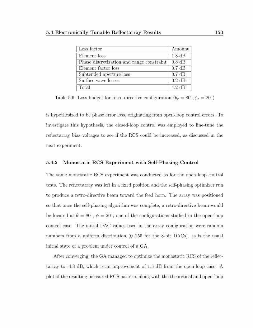
5.4 Electronically Tunable Reflectarray Results 150
Loss factor Amount
Element loss 1.8 dBPhase discretization and range constraint 0.8 dBElement factor loss 0.7 dBSubtended aperture loss 0.7 dBSurface wave losses 0.2 dB
Total 4.2 dB
Table 5.6: Loss budget for retro-directive configuration (θr = 80, φr = 20)
is hypothesized to be phase error loss, originating from open-loop control errors. To
investigate this hypothesis, the closed-loop control was employed to fine-tune the
reflectarray bias voltages to see if the RCS could be increased, as discussed in the
next experiment.
5.4.2 Monostatic RCS Experiment with Self-Phasing Control
The same monostatic RCS experiment was conducted as for the open-loop control
tests. The reflectarray was left in a fixed position and the self-phasing optimizer run
to produce a retro-directive beam toward the feed horn. The array was positioned
so that once the self-phasing algorithm was complete, a retro-directive beam would
be located at θ = 80, φ = 20, one of the configurations studied in the open-loop
control case. The initial DAC values used in the array configuration were random
numbers from a uniform distribution (0–255 for the 8-bit DACs), as is the usual
initial state of a problem under control of a GA.
After converging, the GA managed to optimize the monostatic RCS of the reflec-
tarray to -4.8 dB, which is an improvement of 1.5 dB from the open-loop case. A
plot of the resulting measured RCS pattern, along with the theoretical and open-loop
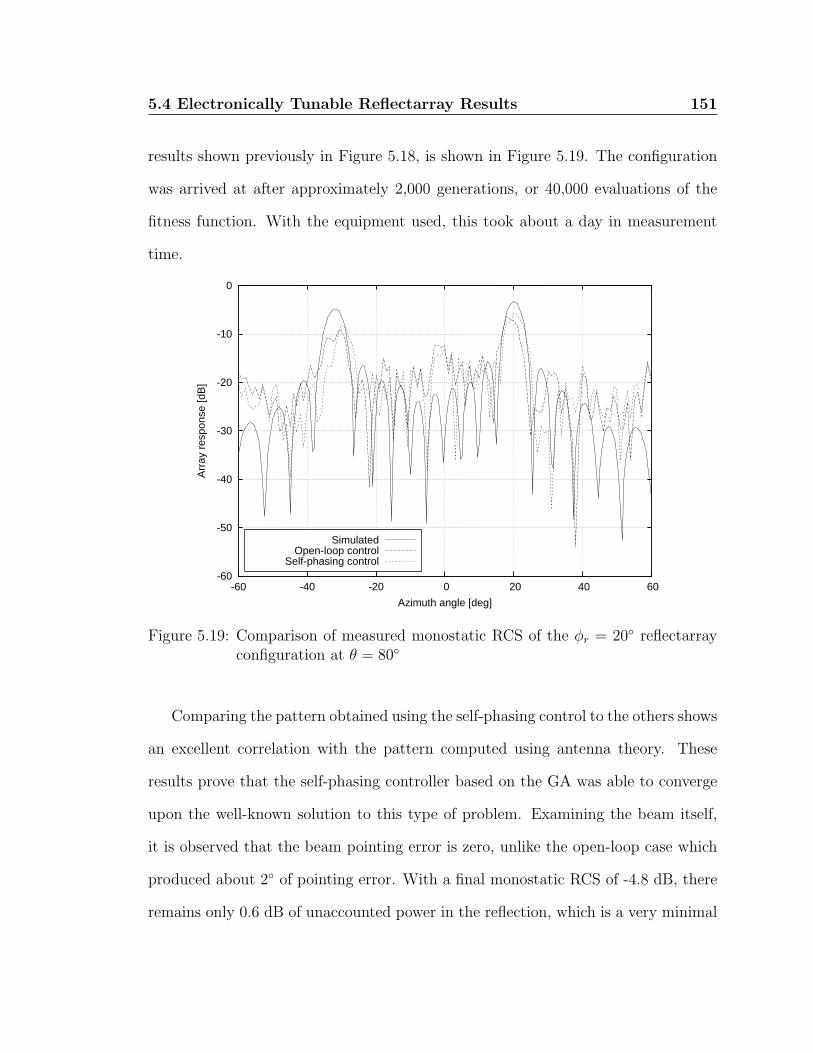
5.4 Electronically Tunable Reflectarray Results 151
results shown previously in Figure 5.18, is shown in Figure 5.19. The configuration
was arrived at after approximately 2,000 generations, or 40,000 evaluations of the
fitness function. With the equipment used, this took about a day in measurement
time.
-60
-50
-40
-30
-20
-10
0
-60 -40 -20 0 20 40 60
Arr
ay r
espo
nse
[dB
]
Azimuth angle [deg]
SimulatedOpen-loop control
Self-phasing control
Figure 5.19: Comparison of measured monostatic RCS of the φr = 20 reflectarrayconfiguration at θ = 80
Comparing the pattern obtained using the self-phasing control to the others shows
an excellent correlation with the pattern computed using antenna theory. These
results prove that the self-phasing controller based on the GA was able to converge
upon the well-known solution to this type of problem. Examining the beam itself,
it is observed that the beam pointing error is zero, unlike the open-loop case which
produced about 2 of pointing error. With a final monostatic RCS of -4.8 dB, there
remains only 0.6 dB of unaccounted power in the reflection, which is a very minimal

5.4 Electronically Tunable Reflectarray Results 152
error. The remaining power was likely lost to the specular reflection produced by
the array. Some of that reflection is visible in Figure 5.17, even despite the fact that
the array is tilted off broadside. Although the measured specular reflection was not
actually integrated to determine the total power loss to specular reflection, 0.6 dB
seems completely reasonable given the over-sized nature of the ground plane, and
possible measurement errors in the anechoic chamber.
5.4.3 Bistatic RCS Experiment with Open-Loop Control
In this experiment, the reflectarray was integrated with an offset feed horn as de-
scribed in Section 5.1.2 and the reflectarray surface scanned like a normal reflector.
A diagram showing the feed scanning arrangement for the reflectarray is shown in
Figure 5.20. The feed horn was placed on an adjustable mount which allowed the
focal distance to be adjusted as needed. The illumination angle of the feed horn, as
well as the height of the reflectarray relative to the feed, could also be adjusted as
necessary.
The whole system was placed on the turntable in the anechoic chamber for bistatic
RCS measurements at a fixed elevation angle. Due to the size of the reflectarray,
only bistatic measurements in the azimuth plane could be performed. The probe
antenna was placed in the chamber such that the reflectarray would have to produce
a beam in the elevation plane of θb = 83.5.
Multiple beam configurations in the azimuth plane were downloaded to the array
controller and used to synthesize test cases for the array. The azimuth angle of
these beams is designated as φb. Open-loop control was used to create these beams.
The phase of the feed illumination pattern used by the the array controller was
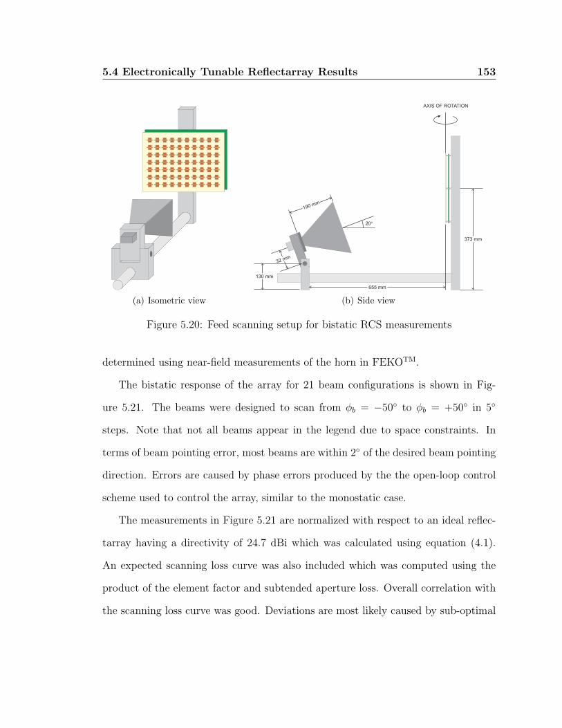
5.4 Electronically Tunable Reflectarray Results 153
(a) Isometric view (b) Side view
Figure 5.20: Feed scanning setup for bistatic RCS measurements
determined using near-field measurements of the horn in FEKOTM.
The bistatic response of the array for 21 beam configurations is shown in Fig-
ure 5.21. The beams were designed to scan from φb = −50 to φb = +50 in 5
steps. Note that not all beams appear in the legend due to space constraints. In
terms of beam pointing error, most beams are within 2 of the desired beam pointing
direction. Errors are caused by phase errors produced by the the open-loop control
scheme used to control the array, similar to the monostatic case.
The measurements in Figure 5.21 are normalized with respect to an ideal reflec-
tarray having a directivity of 24.7 dBi which was calculated using equation (4.1).
An expected scanning loss curve was also included which was computed using the
product of the element factor and subtended aperture loss. Overall correlation with
the scanning loss curve was good. Deviations are most likely caused by sub-optimal
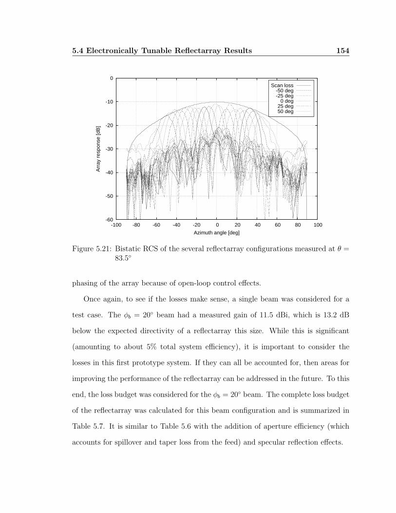
5.4 Electronically Tunable Reflectarray Results 154
-60
-50
-40
-30
-20
-10
0
-100 -80 -60 -40 -20 0 20 40 60 80 100
Arr
ay r
espo
nse
[dB
]
Azimuth angle [deg]
Scan loss-50 deg-25 deg
0 deg25 deg50 deg
Figure 5.21: Bistatic RCS of the several reflectarray configurations measured at θ =83.5
phasing of the array because of open-loop control effects.
Once again, to see if the losses make sense, a single beam was considered for a
test case. The φb = 20 beam had a measured gain of 11.5 dBi, which is 13.2 dB
below the expected directivity of a reflectarray this size. While this is significant
(amounting to about 5% total system efficiency), it is important to consider the
losses in this first prototype system. If they can all be accounted for, then areas for
improving the performance of the reflectarray can be addressed in the future. To this
end, the loss budget was considered for the φb = 20 beam. The complete loss budget
of the reflectarray was calculated for this beam configuration and is summarized in
Table 5.7. It is similar to Table 5.6 with the addition of aperture efficiency (which
accounts for spillover and taper loss from the feed) and specular reflection effects.
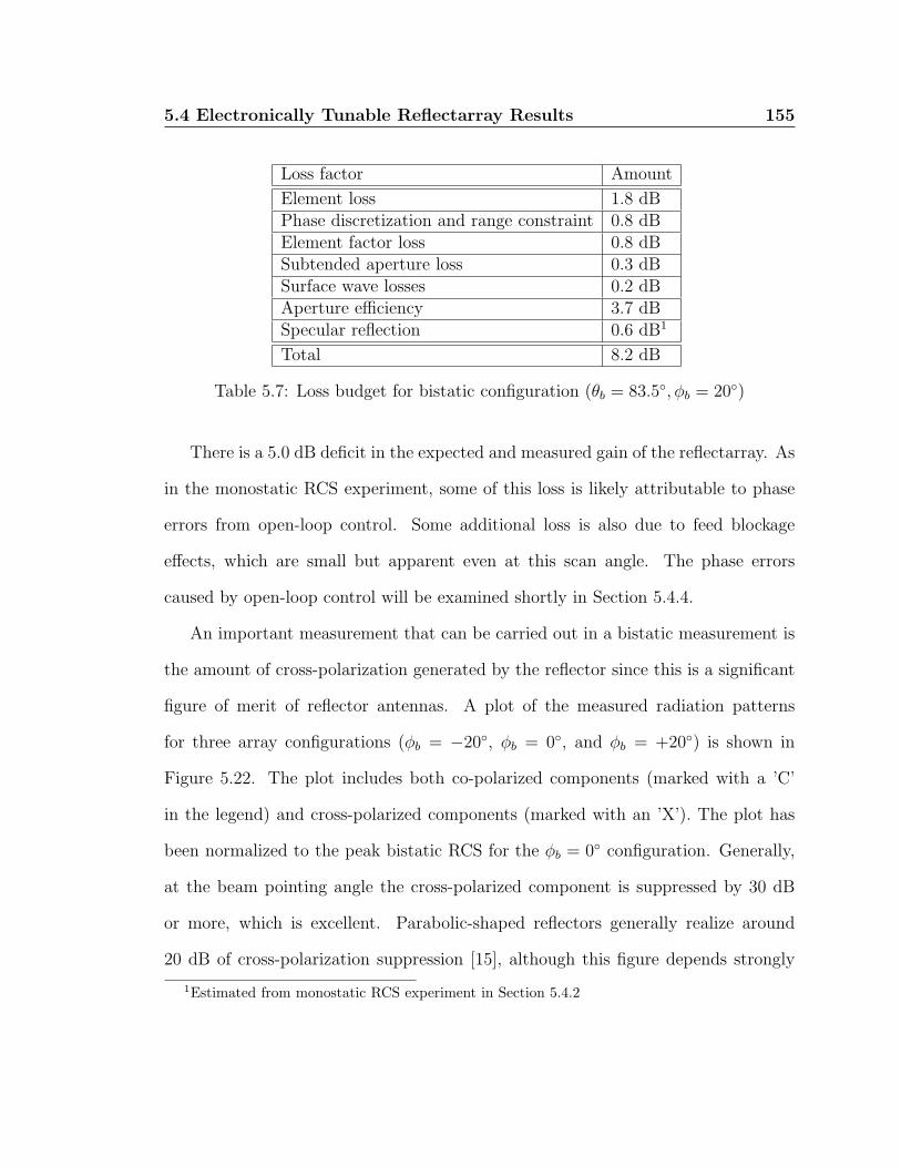
5.4 Electronically Tunable Reflectarray Results 155
Loss factor Amount
Element loss 1.8 dBPhase discretization and range constraint 0.8 dBElement factor loss 0.8 dBSubtended aperture loss 0.3 dBSurface wave losses 0.2 dBAperture efficiency 3.7 dBSpecular reflection 0.6 dB1
Total 8.2 dB
Table 5.7: Loss budget for bistatic configuration (θb = 83.5, φb = 20)
There is a 5.0 dB deficit in the expected and measured gain of the reflectarray. As
in the monostatic RCS experiment, some of this loss is likely attributable to phase
errors from open-loop control. Some additional loss is also due to feed blockage
effects, which are small but apparent even at this scan angle. The phase errors
caused by open-loop control will be examined shortly in Section 5.4.4.
An important measurement that can be carried out in a bistatic measurement is
the amount of cross-polarization generated by the reflector since this is a significant
figure of merit of reflector antennas. A plot of the measured radiation patterns
for three array configurations (φb = −20, φb = 0, and φb = +20) is shown in
Figure 5.22. The plot includes both co-polarized components (marked with a ’C’
in the legend) and cross-polarized components (marked with an ’X’). The plot has
been normalized to the peak bistatic RCS for the φb = 0 configuration. Generally,
at the beam pointing angle the cross-polarized component is suppressed by 30 dB
or more, which is excellent. Parabolic-shaped reflectors generally realize around
20 dB of cross-polarization suppression [15], although this figure depends strongly
1Estimated from monostatic RCS experiment in Section 5.4.2
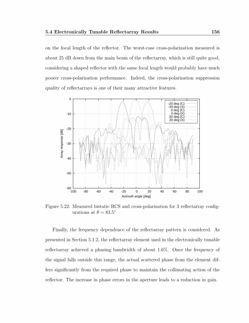
5.4 Electronically Tunable Reflectarray Results 156
on the focal length of the reflector. The worst-case cross-polarization measured is
about 25 dB down from the main beam of the reflectarray, which is still quite good,
considering a shaped reflector with the same focal length would probably have much
poorer cross-polarization performance. Indeed, the cross-polarization suppression
quality of reflectarrays is one of their many attractive features.
-60
-50
-40
-30
-20
-10
0
-100 -80 -60 -40 -20 0 20 40 60 80 100
Arr
ay r
espo
nse
[dB
]
Azimuth angle [deg]
-20 deg (C)-20 deg (X)
0 deg (C)0 deg (X)
20 deg (C)20 deg (X)
Figure 5.22: Measured bistatic RCS and cross-polarization for 3 reflectarray config-urations at θ = 83.5
Finally, the frequency dependence of the reflectarray pattern is considered. As
presented in Section 5.1.2, the reflectarray element used in the electronically tunable
reflectarray achieved a phasing bandwidth of about 1.6%. Once the frequency of
the signal falls outside this range, the actual scattered phase from the element dif-
fers significantly from the required phase to maintain the collimating action of the
reflector. The increase in phase errors in the aperture leads to a reduction in gain.
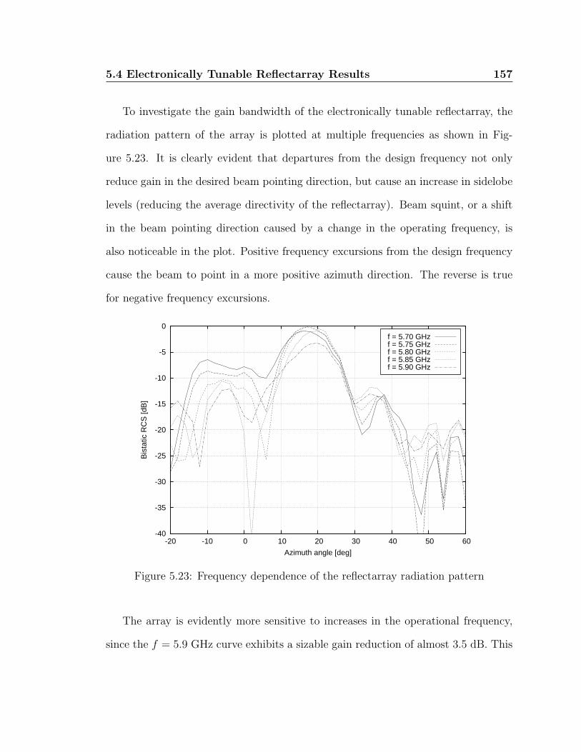
5.4 Electronically Tunable Reflectarray Results 157
To investigate the gain bandwidth of the electronically tunable reflectarray, the
radiation pattern of the array is plotted at multiple frequencies as shown in Fig-
ure 5.23. It is clearly evident that departures from the design frequency not only
reduce gain in the desired beam pointing direction, but cause an increase in sidelobe
levels (reducing the average directivity of the reflectarray). Beam squint, or a shift
in the beam pointing direction caused by a change in the operating frequency, is
also noticeable in the plot. Positive frequency excursions from the design frequency
cause the beam to point in a more positive azimuth direction. The reverse is true
for negative frequency excursions.
-40
-35
-30
-25
-20
-15
-10
-5
0
-20 -10 0 10 20 30 40 50 60
Bis
tatic
RC
S [d
B]
Azimuth angle [deg]
f = 5.70 GHzf = 5.75 GHzf = 5.80 GHzf = 5.85 GHzf = 5.90 GHz
Figure 5.23: Frequency dependence of the reflectarray radiation pattern
The array is evidently more sensitive to increases in the operational frequency,
since the f = 5.9 GHz curve exhibits a sizable gain reduction of almost 3.5 dB. This

5.4 Electronically Tunable Reflectarray Results 158
can be easily explained by the nonlinear dependence of the scattered field phase on
frequency. If the bandwidth over which the reflectarray maintains a gain within
1 dB of the peak gain value, this design achieves this over the frequency range of
5.7− 5.85 GHz. This translates to a 2.5% 1 dB bandwidth which is typical of single-
layer reflectarrays. This bandwidth is slightly larger than the 1.6% phase bandwidth
considered in Section 5.1.2. Therefore, it can be concluded that this phase bandwidth
will give a conservative estimate of the 1-dB bandwidth of the reflectarray.
5.4.4 Bistatic RCS Experiment with Self-Phasing Control
To reduce aperture phase errors, the self-phasing control algorithm was enabled and
used to optimize the φb = 20 configuration. The loss budget for this configuration
was presented in the previous section, and a 5.0 dB error between the expected
and measured gains reported with open-loop control. As for the bistatic case, the
optimizer was initiated for approximately 40,000 iterations of the fitness function,
after which it successfully arrived at the pattern plotted in Figure 5.24.
The resulting beam has no discernible beam pointing error, unlike the open-loop
case which points at φ = 18. Also, the bistatic RCS has increased by 1.4 dB. The
resulting reflectarray configuration has an optimized directivity of 12.9 dBi. This is
a satisfying result, since the beam peak closely approaches the predicted scanning
loss curve unlike the open-loop case. There is about a 0.7 dB difference from the
scanning loss curve, and still 3.6 dB of unaccounted power loss. Further optimization
may yield slightly improved performance, but the more likely cause of the remaining
power deficit is a combination of feed blockage, measurement error in the anechoic
chamber, and a lower-than-expected aperture efficiency.
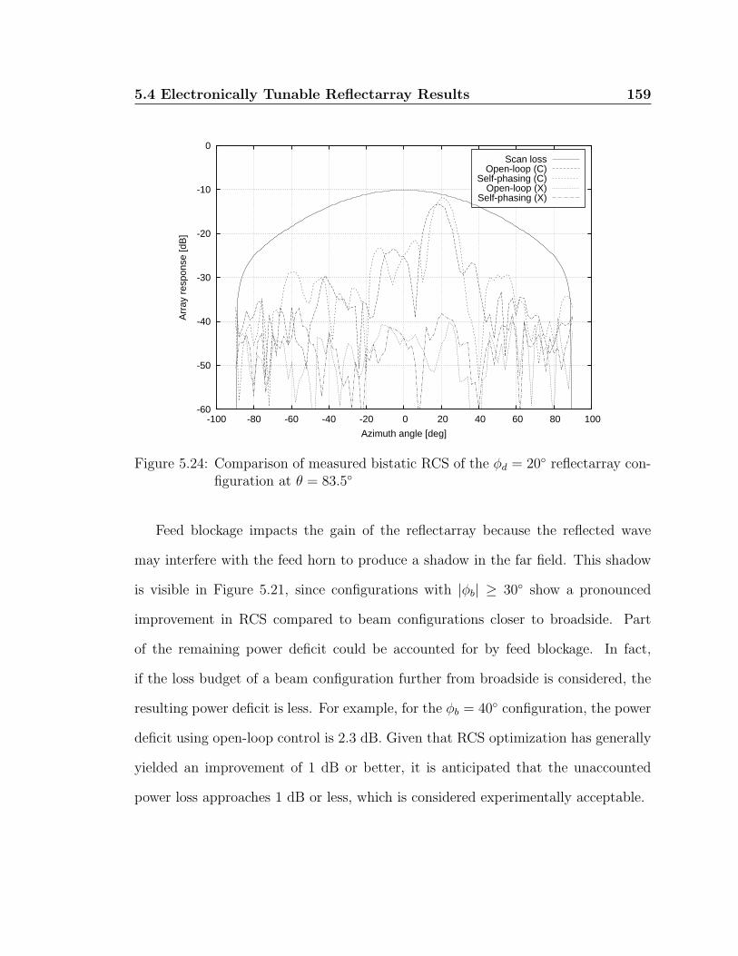
5.4 Electronically Tunable Reflectarray Results 159
-60
-50
-40
-30
-20
-10
0
-100 -80 -60 -40 -20 0 20 40 60 80 100
Arr
ay r
espo
nse
[dB
]
Azimuth angle [deg]
Scan lossOpen-loop (C)
Self-phasing (C)Open-loop (X)
Self-phasing (X)
Figure 5.24: Comparison of measured bistatic RCS of the φd = 20 reflectarray con-figuration at θ = 83.5
Feed blockage impacts the gain of the reflectarray because the reflected wave
may interfere with the feed horn to produce a shadow in the far field. This shadow
is visible in Figure 5.21, since configurations with |φb| ≥ 30 show a pronounced
improvement in RCS compared to beam configurations closer to broadside. Part
of the remaining power deficit could be accounted for by feed blockage. In fact,
if the loss budget of a beam configuration further from broadside is considered, the
resulting power deficit is less. For example, for the φb = 40 configuration, the power
deficit using open-loop control is 2.3 dB. Given that RCS optimization has generally
yielded an improvement of 1 dB or better, it is anticipated that the unaccounted
power loss approaches 1 dB or less, which is considered experimentally acceptable.

5.5 Closing Remarks 160
5.5 Closing Remarks
The experiments discussed in this chapter have validated the electronically tunable
reflectarray concept presented in this thesis. Experiments have not only demon-
strated the agility of the resulting platform, but have also shown that the perfor-
mance of the final structure correlates well with what is expected from theory.
There are some substantial losses that could be reduced in future designs of the
array. Examining Table 5.7, one can notice the most sizable losses in the system
are caused by element loss and poor aperture efficiency. The former loss is primarily
caused by loss in the tuning diode. Techniques for dealing with this type of loss will
be pursued in the next chapter, but if diode losses could be eliminated, the element
loss is estimated to fall to approximately 0.2 dB, which accounts for dielectric and
metal losses. Increasing the aperture efficiency of the reflector is also fairly easy
to implement if a slightly larger reflectarray is constructed to reduce spillover loss.
Theoretically, it should be possible to raise the aperture efficiency to the theoretical
limit of 70% for reflectarrays [15], which would reduce the loss from 3.7 dB to 1.5 dB
and also reduce the effect of feed blockage. Finally, reducing the size of the control
board is anticipated to reduce the specular reflection considerably. All told, if the
losses discussed could be reduced, the loss budgets shown in Table 5.8 could be
potentially realized.
According to the budget, the gain of the system could be increased by 4.4 dB.
Assuming the self-phasing controller was employed, and that the remaining power
deficits discussed could be addressed, approximately 3.8 dB of loss would exist if the
self-phasing controller was employed, yielding an efficiency of approximately 40%,

5.5 Closing Remarks 161
Loss factor Current design Possible
Element loss 1.8 dB 0.2 dBPhase discretization and range constraint 0.8 dB 0.8 dBElement factor loss 0.8 dB 0.8 dBSubtended aperture loss 0.3 dB 0.3 dBSurface wave losses 0.2 dB 0.2 dBAperture efficiency 3.7 dB 1.5 dBSpecular reflection 0.6 dB 0 dB
Total loss 8.2 dB 3.8 dB
Table 5.8: Hypothetically improved loss budget for bistatic configuration (θb =83.5, φb = 20)
which is competitive with fixed reflectarrays. Even if diode losses remained, an overall
system efficiency of 29% could still be achieved. However, the reduced efficiency in
exchange for electronic reconfigurability is felt to be well worth the cost.
One point deserving some discussion is the potential of the self-phasing controller.
In the experiments discussed in this chapter, the control was used purely to compen-
sate for intrinsic errors with the reflectarray to reduce aperture phase errors. In this
capacity, the controller worked very well, improving the gain of the reflectarray to
the expected limit within the context of other losses. The ability of the controller to
deal with intrinsic errors in the reflectarray improves the robustness of the system
since errors in the elements, feed, and illumination pattern can all be addressed by
the controller in the event of a departure from expected behaviour.
One can take this behaviour one step further and utilize self-phasing control to
provide the reflectarray with a degree of fault tolerance. The self-phasing feature can
allow the reflectarray to effectively adapt to faults such as element failures since a
self-phasing reflectarray will continue to produce a beam pattern (albeit with reduced

5.5 Closing Remarks 162
gain) if some of the elements fail. Similarly, the reflectarray possesses fault tolerance
with regards to the feed horn alignment: if the feed horn is moved away from the
focal point for some reason, the controller can simply adapt the reflector surface and
effective move the focal point to the new position. The self-phasing feature plus the
inherent hardware simplicity of reflectarrays makes them favourable candidates for
fault-tolerant antennas. Though the fault tolerance of the array was not investigated
in any major depth in this study, it is an interesting topic for future research.

Chapter 6
Recent Developments and Future Work
The electronically tunable reflectarray element has been shown to demonstrate
excellent scattering characteristics. On their own, the cells exhibit excellent
phase agility, large enough to enable beam-forming applications with reflectarrays.
Embedded in an electronically tunable reflectarray, the system exhibits the expected
level of performance and substantial potential for both space-borne and terrestrial
applications.
This chapter examines future work that can be conducted with the electronically
tunable reflectarray prototype. The first line of research that is considered is the
improvement of the reflectarray element itself. The foundation for future work in
this area has already been laid through some preliminary experiments, which will be
presented in detail in the first part of this chapter. The second part contemplates
future work that could be pursued at the array level. Alternative reflectarray con-
figurations and applications will be discussed. Additionally, some applications and
implications of the control algorithms that were used in Chapter 5 will be presented.
6.1 Possible Reflectarray Element Improvements
The reflectarray element topology that has been presented in this thesis, while ex-
hibiting a high level of phase agility, is not without some disadvantages as well. One
of these issues has already been identified, which is the loss associated with the tun-
6.1 Possible Reflectarray Element Improvements 164
ing diode which has a large impact on the efficiency of the reflectarray. The other
issue is the linearity of the cell with regards to the relationship between the inci-
dent and reflected signals. Since the tuning of the element is based on a device that
is inherently nonlinear, this could raise potential issues when using reflectarrays in
medium- to high-power applications such as transmitters. Since this effect has not
yet been contemplated, we begin with a characterization of the linear performance
of the reflectarray cell.
6.1.1 Reflectarray Element Linearity
The reflectarray element presented throughout this thesis has the potential to exhibit
nonlinear characteristics, due to the nature of the varactor diode used for tuning the
element. The ability to change the capacitance of the varactor diode has been the
pivotal aspect of the electronically tunable reflectarray cell design. By changing
the reverse DC bias applied to the diode, its capacitance is changed. However, the
diode can also be subject to changes in capacitance in response to a large radio
frequency signal. Since currents and fields are established on and around the patch
near its resonant frequency, a potentially large time-varying voltage superimposed
on top of the DC bias voltage can be established across the diode. Hence, the
capacitance produced by the varactor diode will not be fixed, but vary in accordance
with this time-varying voltage. That is, the capacitance of the varactor diode will
be modulated by the time-varying voltage across the diode. If the incident field is
small, the amount of capacitance modulation will be insignificant. However, beyond
a certain threshold, the modulation of the capacitance will also begin to modulate
the phase of the reflected signal significantly, leading to reflected signal distortion.
6.1 Possible Reflectarray Element Improvements 165
Signal distortion in communication systems is a significant issue because inter-
modulation distortion from nonlinear components such as mixers and amplifiers can
dramatically increase the bandwidth of the output signal. This necessitates the use
of filters in communication systems to suppress the distortion. However, in the case
of a transmitting reflectarray, filters cannot be used to deal with signal distortion
because the antenna is the final element in the communications chain. Therefore,
even if the input signal to the reflectarray is perfectly linear or filtered, the reflectar-
ray will introduce its own distortion which cannot be removed from the transmitted
signal.
To quantify the amount of distortion created by a component or system, two
types of distortion measurements are used: a harmonic distortion test and an in-
termodulation distortion test. In a harmonic distortion test, the cell is subject to a
monochromatic input signal and the creation of harmonics is examined. This type of
distortion is not the major point of interest for this study, since the distortion tends
to be out-of-band for most systems where this antenna would be employed. Inter-
modulation distortion (IMD), which is distortion created by the mixing of multiple
input frequencies as a result of the nonlinearity in the device under test (DUT), is
of major interest, since the amount of spectral broadening can be directly measured
in this type of measurement.
One of the standard ways of characterizing IMD is to use a two-tone test, whereby
the DUT is subjected to an input signal consisting of two sinusoids closely spaced in
frequency. Due to the nonlinear nature of the device, the output signal will consist
of various distortion products at frequencies of mf1 − nf2 and nf1 −mf2, where f1
and f2 denote the frequencies of the input sinusoids, and m,n = 1, 2, 3, . . .. The
6.1 Possible Reflectarray Element Improvements 166
sum m+n is referred to as the order of the IMD. Usually, odd-order distortion is of
most interest since those products are close in frequency to the input signals, while
the even-order distortion is usually out of band. For example, 3rd-order IMD, or
IM3, exists at frequencies 2f1 − f2 and 2f2 − f1, which are directly adjacent to the
two input frequencies. Since IM3 is the distortion with the most adjacent frequency
components, it is usually examined the most closely, though IM5 can be considered
as well.
To test the IMD generated by the reflectarray, a rectangular waveguide cell mea-
surement setup based on the one presented in Section 3.4 was used. The setup of this
system is shown in Figure 6.1. Two signal sources are used to create the two input
tones which are added together before they are launched into the waveguide. The
reflected signal is separated from the incident signal using a directional coupler and
sampled using a spectrum analyzer to isolate the various intermodulation products.
The IMD generated by the reflectarray cell is anticipated to be a function of sev-
eral variables. The most obvious variable is the input power applied to the waveguide:
the greater the power, the greater the capacitance modulation effect, and the greater
the expected distortion in the reflected signal. The IMD is also hypothesized to be
a strong function of the bias voltage supplied to the varactor diode. If the diode
is biased in the centre of the phase characteristic, where the phase slope is highest,
then small modulation of the varactor bias by an RF signal produces large changes in
reflection phase, and hence greater distortion. Conversely, when the diode is biased
away from the resonance in the phase characteristic, less distortion is expected in
the reflected signal.
Third order and fifth order IMD was recorded in the experiment using f1, f2 =
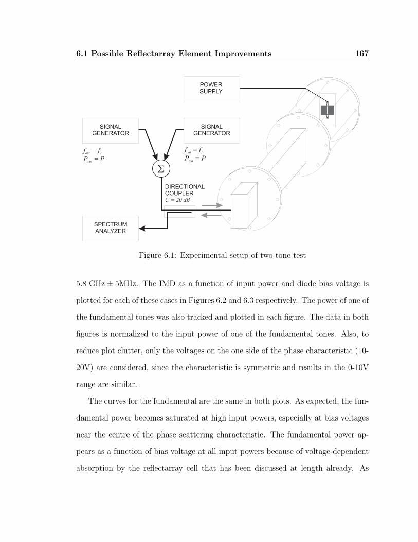
6.1 Possible Reflectarray Element Improvements 167
Figure 6.1: Experimental setup of two-tone test
5.8 GHz ± 5MHz. The IMD as a function of input power and diode bias voltage is
plotted for each of these cases in Figures 6.2 and 6.3 respectively. The power of one of
the fundamental tones was also tracked and plotted in each figure. The data in both
figures is normalized to the input power of one of the fundamental tones. Also, to
reduce plot clutter, only the voltages on the one side of the phase characteristic (10-
20V) are considered, since the characteristic is symmetric and results in the 0-10V
range are similar.
The curves for the fundamental are the same in both plots. As expected, the fun-
damental power becomes saturated at high input powers, especially at bias voltages
near the centre of the phase scattering characteristic. The fundamental power ap-
pears as a function of bias voltage at all input powers because of voltage-dependent
absorption by the reflectarray cell that has been discussed at length already. As
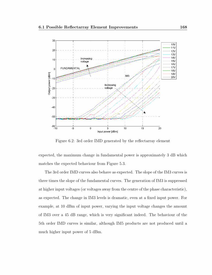
6.1 Possible Reflectarray Element Improvements 168
Figure 6.2: 3rd order IMD generated by the reflectarray element
expected, the maximum change in fundamental power is approximately 3 dB which
matches the expected behaviour from Figure 5.3.
The 3rd order IMD curves also behave as expected. The slope of the IM3 curves is
three times the slope of the fundamental curves. The generation of IM3 is suppressed
at higher input voltages (or voltages away from the centre of the phase characteristic),
as expected. The change in IM3 levels is dramatic, even at a fixed input power. For
example, at 10 dBm of input power, varying the input voltage changes the amount
of IM3 over a 45 dB range, which is very significant indeed. The behaviour of the
5th order IMD curves is similar, although IM5 products are not produced until a
much higher input power of 5 dBm.
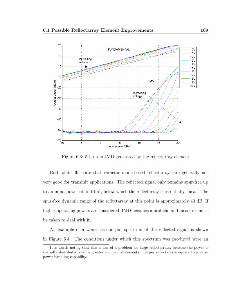
6.1 Possible Reflectarray Element Improvements 169
Figure 6.3: 5th order IMD generated by the reflectarray element
Both plots illustrate that varactor diode-based reflectarrays are generally not
very good for transmit applications. The reflected signal only remains spur-free up
to an input power of -5 dBm1, below which the reflectarray is essentially linear. The
spur-free dynamic range of the reflectarray at this point is approximately 40 dB. If
higher operating powers are considered, IMD becomes a problem and measures must
be taken to deal with it.
An example of a worst-case output spectrum of the reflected signal is shown
in Figure 6.4. The conditions under which this spectrum was produced were an
1It is worth noting that this is less of a problem for large reflectarrays, because the power isspatially distributed over a greater number of elements. Larger reflectarrays equate to greaterpower handling capability.
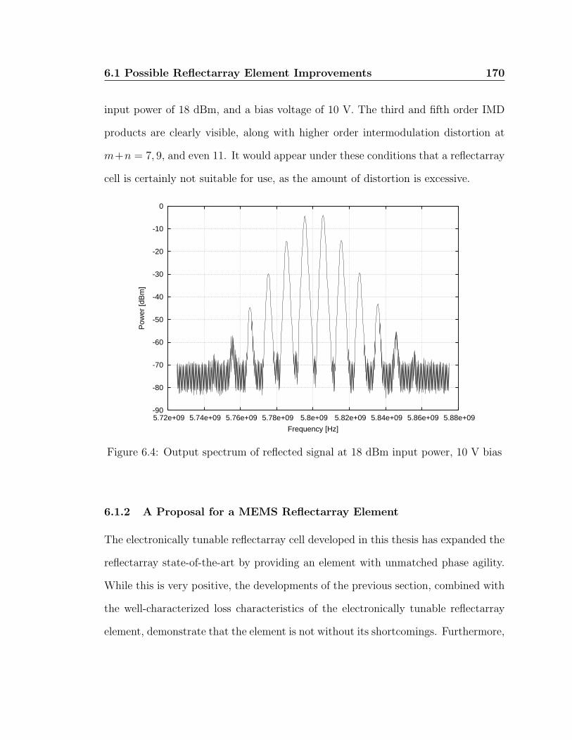
6.1 Possible Reflectarray Element Improvements 170
input power of 18 dBm, and a bias voltage of 10 V. The third and fifth order IMD
products are clearly visible, along with higher order intermodulation distortion at
m+n = 7, 9, and even 11. It would appear under these conditions that a reflectarray
cell is certainly not suitable for use, as the amount of distortion is excessive.
-90
-80
-70
-60
-50
-40
-30
-20
-10
0
5.72e+09 5.74e+09 5.76e+09 5.78e+09 5.8e+09 5.82e+09 5.84e+09 5.86e+09 5.88e+09
Pow
er [d
Bm
]
Frequency [Hz]
Figure 6.4: Output spectrum of reflected signal at 18 dBm input power, 10 V bias
6.1.2 A Proposal for a MEMS Reflectarray Element
The electronically tunable reflectarray cell developed in this thesis has expanded the
reflectarray state-of-the-art by providing an element with unmatched phase agility.
While this is very positive, the developments of the previous section, combined with
the well-characterized loss characteristics of the electronically tunable reflectarray
element, demonstrate that the element is not without its shortcomings. Furthermore,

6.1 Possible Reflectarray Element Improvements 171
it is anticipated that extending the technology to millimetre-wave frequencies will not
be simply a matter of scaling the design, primarily due to substantial diode package
parasitics at these frequencies that will limit its operation. This has motivated some
research into new technology that could be incorporated into the tunable cell concept
to address these issues.
Tuning capacitors based on micro-electro-mechanical systems (MEMS) can ad-
dress many of these issues. Since MEMS capacitors exhibit a very high quality factor,
employing MEMS capacitors in place of semiconductor tuning diodes is expected to
reduce reflection losses substantially. Being a mechanical device, the MEMS devices
are also immune to capacitance modulation effects at the carrier frequency, virtually
eliminating nonlinear distortion and allowing the reflectarray to be employed as a
transmit antenna. Furthermore, a reflectarray element based on a MEMS capac-
itors has the added advantage of potentially being monolithically integrated in a
single process. Integrating the patch with the tuning element enables reflectarrays
to operate at frequencies higher than would be possible with packaged components.
To explore this possibility, a collaborative research project was initiated between
the author and a graduate student in the same research group, Greg McFeetors, who
specializes in MEMS capacitors. The goal was to monolithically integrate MEMS
capacitors with the patch in a single fabrication process and investigate the feasibility
of using MEMS components in a reflectarray application.
A reflectarray cell based on a MEMS capacitor was designed. The MEMS capaci-
tor, previously presented in [77], is based on the bridge structure shown in Figure 6.5.
Capacitance is developed between two plates, one of which can be displaced using
electrostatic force by applying voltage across the points labelled “Tune2” in the fig-

6.1 Possible Reflectarray Element Improvements 172
ure. Further displacement can be achieved by applying the same voltage to the
points labelled “Tune1” on the capacitor. The capacitor was designed to match the
capacitance range of the varactor diode previously used. Greater than 5:1 tuning
range had been demonstrate with this MEMS capacitor in other experiments so the
cell was anticipated to provide a substantial phase tuning range.
Figure 6.5: Structure of the MEMS capacitor (figure courtesy Greg McFeetors)
The capacitor was designed into the previously presented cell topology, directly
replacing the varactor diodes in the design. For comparison purposes to the previous
varactor-based cells presented in Chapter 3, the cell was designed for operation at
5.5 GHz. The patch and integrated capacitors are fabricated in the same process on
a 1500 µm fused silica substrate (εr = 3.8), which is actually realized from fusing
three 500 µm substrates together. On this substrate, the required design dimensions
for operation at 5.5 GHz were L = 17 mm, W = 14 mm, and g = 0.5 mm.
The reflectarray element was fabricated at micro-fabrication facilities at the Uni-
versity of Calgary and University of Alberta. A photograph of one side of the com-
plete cell, with an inset showing the MEMS capacitor, is shown in Figure 6.6. An
off-chip biasing structure based on the same network used for the varactor diode-
based cell (not shown) decouples the DC tuning voltage from the RF currents on the
patch.
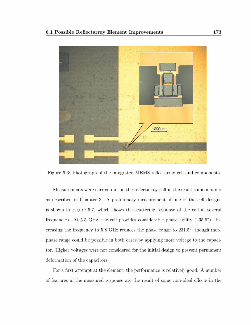
6.1 Possible Reflectarray Element Improvements 173
Figure 6.6: Photograph of the integrated MEMS reflectarray cell and components
Measurements were carried out on the reflectarray cell in the exact same manner
as described in Chapter 3. A preliminary measurement of one of the cell designs
is shown in Figure 6.7, which shows the scattering response of the cell at several
frequencies. At 5.5 GHz, the cell provides considerable phase agility (265.6). In-
creasing the frequency to 5.8 GHz reduces the phase range to 231.5, though more
phase range could be possible in both cases by applying more voltage to the capaci-
tor. Higher voltages were not considered for the initial design to prevent permanent
deformation of the capacitors.
For a first attempt at the element, the performance is relatively good. A number
of features in the measured response are the result of some non-ideal effects in the
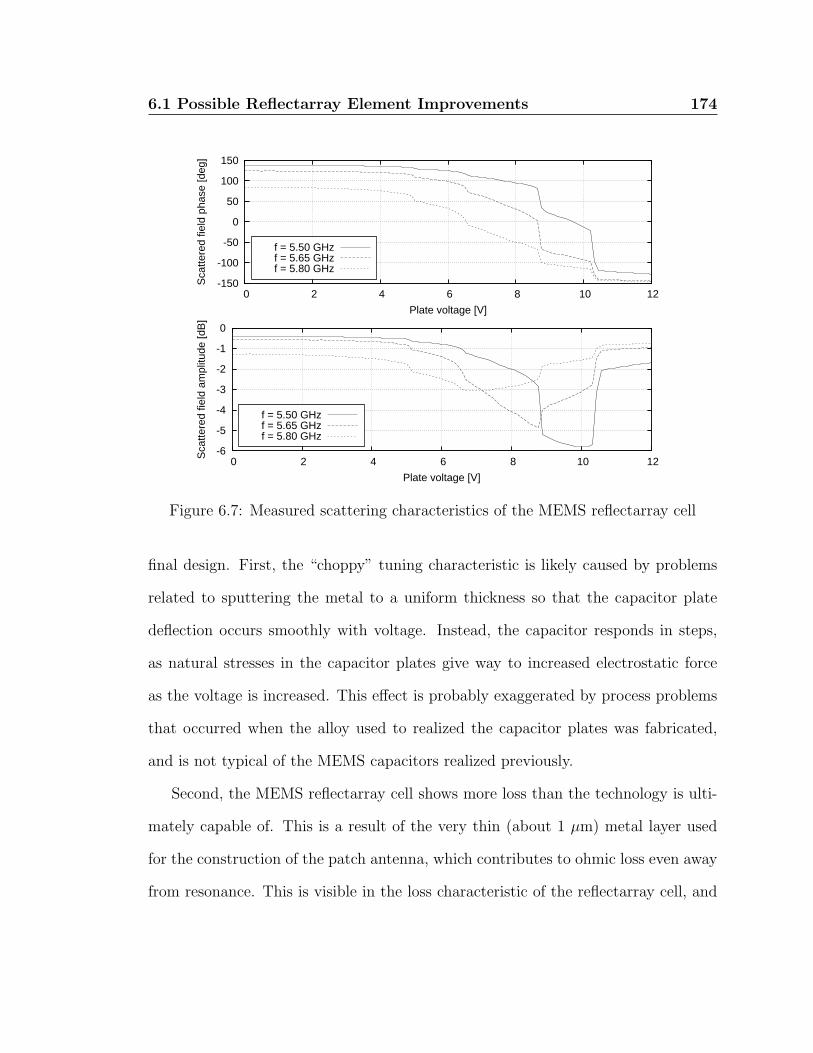
6.1 Possible Reflectarray Element Improvements 174
-6
-5
-4
-3
-2
-1
0
0 2 4 6 8 10 12Sca
ttere
d fie
ld a
mpl
itude
[dB
]
Plate voltage [V]
f = 5.50 GHzf = 5.65 GHzf = 5.80 GHz
-150
-100
-50
0
50
100
150
0 2 4 6 8 10 12
Sca
ttere
d fie
ld p
hase
[deg
]
Plate voltage [V]
f = 5.50 GHzf = 5.65 GHzf = 5.80 GHz
Figure 6.7: Measured scattering characteristics of the MEMS reflectarray cell
final design. First, the “choppy” tuning characteristic is likely caused by problems
related to sputtering the metal to a uniform thickness so that the capacitor plate
deflection occurs smoothly with voltage. Instead, the capacitor responds in steps,
as natural stresses in the capacitor plates give way to increased electrostatic force
as the voltage is increased. This effect is probably exaggerated by process problems
that occurred when the alloy used to realized the capacitor plates was fabricated,
and is not typical of the MEMS capacitors realized previously.
Second, the MEMS reflectarray cell shows more loss than the technology is ulti-
mately capable of. This is a result of the very thin (about 1 µm) metal layer used
for the construction of the patch antenna, which contributes to ohmic loss even away
from resonance. This is visible in the loss characteristic of the reflectarray cell, and

6.1 Possible Reflectarray Element Improvements 175
can be easily alleviated in the future with electroplating.
The linearity of the MEMS reflectarray element was also measured, and as ex-
pected, the spectrum was free of any intermodulation distortion. Since no IMD was
present, a plot of IMD was not reproduced here. This fact, combined with the fact
that cell loss in future versions of the reflectarray is anticipated as being much lower,
makes this cell structure a very interesting and attractive topic for future research
and development. Experimentation with the capacitor structure and fabrication
should also enable the phase range of the device to be extended, especially given the
fact that MEMS capacitors of this type demonstrate substantial tuning ranges when
measured on their own.
Overcoming engineering problems with the MEMS reflectarray cell promises to
open up very interesting possibilities for reconfigurable reflectarrays in the future.
Their linear nature and low loss will enable tunable reflectarrays to exhibit efficiencies
competitive with fixed reflectarrays, provided integrated cells can be fabricated in
arrays with high yield. Indeed, the future appears promising in this fascinating area
of research.
6.1.3 Other Cell Possibilities
A number of other possibilities have been contemplated as cell topologies for future
versions of the electronically tunable reflectarray. Most of these ideas, like the MEMS
idea, stem from underlying limitations in the basic tunable cell topology. A summary
of these limitations includes:
• Reflectarray cell loss, which results from the lossy characteristics of the tuning
diode

6.1 Possible Reflectarray Element Improvements 176
• Reflectarray cell linearity
• Limited phase tuning range / bandwidth
• No independent amplitude control of cells
• Packaging effects at high frequencies
There are a number of ways that some or all of these limitations could be ad-
dressed in future developments of the reflectarray element. These ideas include:
1. Active reflectarray elements. Reflectarray cell loss can be potentially alle-
viated using low-loss tuning components based on MEMS, as already presented.
An alternative is to use active components in the reflectarray cell, which can
not only compensate for element loss, but provide amplification as well. The
idea of an active reflectarray cell is certainly not new, and originates from ideas
in spatial power combining [78] whereby free space is used as the distribution
network for power combiners much in the same way a reflectarray uses it to
distribute feeding signals to antenna elements. By adding gain to a reflectar-
ray, then, it becomes possible to address the power distribution problem in
amplifiers while simultaneously focusing the power into a coherent beam for
antenna applications. Active reflectarray elements have been contemplated in
the literature [79]-[81]. However, while gain is provided, the beam is fixed just
as is the case with most passive reflectarray architectures. If a variable phase
shift could be introduced to these elements, then a truly versatile reconfig-
urable antenna platform would have been produced. Instead of having to use

6.1 Possible Reflectarray Element Improvements 177
a large (and likely expensive) power amplifier at the feed horn, the amplifica-
tion can be spatially distributed, which not only alleviates costs but enables
much higher output powers to be contemplated (as in the case of spatial power
combiners). This area of research is germane for future research.
2. Multi-layer tunable reflectarray elements. While the current reflectarray
element design covers most of the 360 range required, adding more phase range
would like reduce the phase errors noted in Chapter 5, and also increase the
bandwidth of large reflectarrays as in the case of stacked patch reflectarrays. In
fact, a reconfigurable stacked patch reflectarray would be a fascinating concept
to pursue in the future, as a means for addressing this issue.
3. Independent amplitude control of reflectarray elements. Amplitude
control of the elements is currently not possible in the current realization of
the reconfigurable antenna platform. Though amplitude variation has been
demonstrated with the unit cell, it is undesirable because it is dependent on the
tuned phase of the cell. Ideally, these two attributes of the unit cell should be
independently controllable. Amplitude control could enable complex pattern
synthesis problems to be handled by the reflectarray. Since amplitude response
manipulation of reflectarrays has been demonstrated in fixed form [34], it would
be interesting to adapt the topology in this platform to a tunable form.
4. Distributed tuning techniques. As mentioned in Section 6.1.2, migrating
the tunable reflectarray cell to high frequencies is a significant issue, compared
to the design of fixed reflectarrays at the same frequency. Since discrete com-
ponents must be integrated with the reflectarray antenna elements, there are

6.2 Future Work at the Array Level 178
engineering issues related to this problem that must be resolved. Monolithic
integration of the tuning element with the cell is one possible technique (as in
the case of MEMS), but other distributed techniques could be investigated to
enable operation at higher frequencies in the future. Distributed tuning would
also make the elements less sensitive to losses in lumped components.
6.2 Future Work at the Array Level
The viability of the electronically tunable reflectarray concept also opens up a vari-
ety of opportunities for further development at the array level. Future possibilities
include investigating alternative geometries for the reflectarray, and exploring the
use of the self-phasing reflectarray for other applications. Both of these ideas are
discussed in the following sections.
6.2.1 Alternative Reflectarray Geometries
While the tunable reflectarray is a very flexible reconfigurable antenna platform,
because of its reflector-like geometry it is limited to scan angles in front of the
reflector. Furthermore, scanning loss introduced by the microstrip patch elements,
as well as subtended aperture loss, constrains the scanning range of the reflectarray
to within ±50 of broadside. An ultimate embodiment of a reconfigurable antenna
would support beam-forming in all directions.
To do this, a transmit-array architecture could be considered, whereby the feed
antenna illuminates a number of re-radiators surrounding the feed in all directions.
An example of how this might be done is shown conceptually in Figure 6.8, though
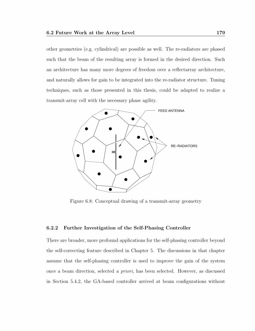
6.2 Future Work at the Array Level 179
other geometries (e.g. cylindrical) are possible as well. The re-radiators are phased
such that the beam of the resulting array is formed in the desired direction. Such
an architecture has many more degrees of freedom over a reflectarray architecture,
and naturally allows for gain to be integrated into the re-radiator structure. Tuning
techniques, such as those presented in this thesis, could be adapted to realize a
transmit-array cell with the necessary phase agility.
FEED ANTENNA
RE−RADIATORS
Figure 6.8: Conceptual drawing of a transmit-array geometry
6.2.2 Further Investigation of the Self-Phasing Controller
There are broader, more profound applications for the self-phasing controller beyond
the self-correcting feature described in Chapter 5. The discussions in that chapter
assume that the self-phasing controller is used to improve the gain of the system
once a beam direction, selected a priori, has been selected. However, as discussed
in Section 5.4.2, the GA-based controller arrived at beam configurations without

6.2 Future Work at the Array Level 180
any prior knowledge of the desired beam direction – the reflectarray elements were
randomized and a useful configuration determined by the optimizer. This allows self-
phasing reflectarrays to potentially form beams without any prior knowledge of the
external terminal’s location. Essentially, the reflectarray becomes a “self-pointing”
reflector whereby the desired beam locks on to the terminal and a beam formed in
that location automatically.
Self-phasing also allows the antenna to adapt to changes in the received signal.
These changes could be caused by terminal movement, or even multipath effects in
the radio channel. The adaptive nature of the self-phasing control results in the
antenna to produce an array response that maximizes signal power at the feed horn
regardless of source conditions. In a multipath environment, the reflectarray could
actually produce multiple beams pointed in the directions of signal arrival and co-
phase the signals properly to mitigate the effect of multipath fading. The effect is
directly analogous to the use of a receiver employing a diversity combining technique
known as equal gain combining [82], and can be used to provide the system with
diversity gain.
From this discussion it can be seen that the self-phasing reflectarray has signifi-
cant potential for effectively dealing with environmental effects, addressing terminal
movement, and providing self-pointing functionality without knowledge of source
conditions. While these applications were not investigated in detail in this thesis,
there is obviously significant potential for investigating these applications in the fu-
ture. In particular, adapting to multipath conditions, as well as dealing with terminal
movement, are seen as being challenging problems that if solved, will increase the
potential applications of this reconfigurable antenna platform.

Chapter 7
Conclusions
Areconfigurable antenna platform for producing electronically controllable ra-
diation patterns has been presented in this thesis. This antenna is realized
using a unique blend of concepts from antenna arrays and reflector antennas, in a
platform known as a reflectarray antenna. Though traditionally, reflectarrays pre-
sented in the literature have only been able to realize reflectors with fixed antenna
patterns, this thesis has proved that the antenna elements in a reflectarray can be
made to be electronically tunable, allowing reflectarrays to scan the beam electron-
ically. The resulting platform boasts a number of key advantages over traditional
antenna arrays, including lower cost, fewer components, spatial feeding, and easy
integration with closed-loop control systems for managing the radiation pattern.
7.1 Research Achievements
Recall from Chapter 1, Section 1.3, that the goals of the thesis were threefold:
1. To develop a phase agile reflectarray cell and fully understand its operation
and design;
2. To enhance the understanding of array-level effects in reflectarrays such as
sources of loss, specular reflections, and transient effects;
3. To successfully demonstrate experimentally the feasibility of using electroni-

7.1 Research Achievements 182
cally tunable reflectarrays as reconfigurable antennas.
These goals have been met in this study, and the specific achievements in meeting
these goals are now discussed.
The key to the operation of the platform is the electronically tunable reflectar-
ray cell. Previous attempts in the literature demonstrated tunable reflectarray cells
with inadequate phase agility to be considered useful for beam-forming applications.
This thesis has presented the design of a novel electronically tunable reflectarray cell
that possesses excellent phase agility and other scattering characteristics for use in
electronically tunable reflectarrays. A number of comprehensive techniques for the
analysis and design of electronically tunable reflectarray cells were presented in the
thesis. These techniques include an extensive equivalent circuit model, and various
computational electromagnetics models. Combined, these techniques ultimately en-
abled a reflectarray element with superior phase agility to be realized in this work
and has enhanced the understanding of scattering dynamics of reflectarray elements
in the field.
Analytical and numerical analysis at the array level has demonstrated the mer-
its of this unique reconfigurable antenna platform. The detailed development of a
computational electromagnetics model of an infinite reflectarray has enhanced the
understanding of numerous effects in reflectarrays that are of great importance when
considering the design of an electronically tunable form of this architecture. In partic-
ular, the understanding of specular reflections from reflectarrays has been enhanced
through this work and has proved that a reconfigurable antenna platform based on
the proposed cell design will not suffer significantly from this form of loss. This

7.1 Research Achievements 183
model has also enabled transient effects in reflectarrays to be better understood.
Two experimental prototypes demonstrating the proposed reflectarray cell oper-
ating in an array have been presented. The first prototype, based on a fixed form
of the reflectarray element, validated the initial cell concept and proved that beam-
forming with the proposed cell topology was viable. The second prototype, which
was fully electronically tunable, demonstrated the outstanding beam-forming capa-
bilities of the platform. Detailed experiments examining the monostatic and bistatic
radar cross section of the electronically tunable reflectarray prototype demonstrated
that its performs equals what is expected from theory and the models presented in
the thesis. The validation of these models allows improved forms of the reflectarray
to be designed in the future, exhibiting even better performance. Additionally, a
control system for reducing phase errors in an electronically tunable reflectarray has
been shown to improve performance with a simple, straightforward algorithm.
The electronically tunable experimental prototype realized in this thesis illus-
trates good performance considering it is the first realization of an antenna of this
type. The 70-element prototype provided over 100 of beam scanning range in the
azimuth plane, and provided a 2.5% 1-dB gain bandwidth at 5.8 GHz. It exhibited a
peak gain of approximately 12 dBi, and while there were more than 8 dB in estimated
losses, most of these can be easily addressed through the design of a better feeding
system, increased reflectarray size, and board sizes with reduced specular reflection.
The peak efficiency of the system is estimated at 15% though it is anticipated that
basic changes to the prototype could improve this to 29%.
An analysis of issues affecting the performance of electronically tunable reflectar-
rays revealed that one of the single best ways to improve performance is to reduce

7.2 Thesis Contributions 184
reflection loss from the reflectarray elements. If this were possible, the efficiency of
the electronically tunable reflectarray could be improved to 40%, which is compet-
itive with fixed forms. The elements are also susceptible to nonlinear effects which
can make electronically tunable reflectarrays undesirable as high-power transmitting
antennas. To address these problems, a preliminary study was undertaken to in-
vestigate the feasibility of using MEMS devices integrated with the reflectarray cell.
Preliminary results from this study have demonstrated the potential MEMS devices
possess with regards to solving these problems. This work has solidified the founda-
tion for further developments in MEMS reflectarray antennas, and is also a world’s
first in experimentally demonstrated reflectarray technology.
7.2 Thesis Contributions
This thesis had made a number of major contributions to the field of reflectarrays.
As discussed earlier, the concept of an electronically tunable reflectarray element,
while not completely new, is a topic of primarily theoretical and conceptual dis-
cussions in the literature. Practical realizations pursued by researchers failed to
provide the scattering characteristics necessary to make reflectarrays fully tunable.
The contributions in this thesis have resulted in a number of publications. The first
disclosure of the concept lead to an award-winning paper [83], which was later ex-
panded upon [84][85]. Initial publication of these ideas inspired other researchers to
investigate a similar tunable element structure [86].
The development of the equivalent circuit model, and self-phasing array controller
was also presented recently in [87] and [88], respectively. FDTD modelling of the
7.2 Thesis Contributions 185
infinite reflectarrays is also pending presentation [89]. Preliminary research into the
MEMS reflectarray cells has resulted in two pending presentations [90][91], one of
which is invited.
An interesting collaborative project, outside the scope of this thesis, has also
been pursued between the author and another researcher and has enhanced the
state-of-the-art in the area of reflectarray applications. This project investigated the
feasibility of using reconfigurable antennas (including electronically tunable reflec-
tarrays) to realize systems employing space-time coding. Space-time coding is used
to improve the capacity of wireless communication systems, but is often expensive
to implement because of the need for multiple transmit modules. Since the one of
the major advantages of electronically tunable reflectarrays is that array processing
can be performed without the need for multiple transmit/receive modules, it became
clear that these systems, and reconfigurable antennas in general, could potentially
address a problem in space-time coding.
One of the core operations in space time coding is independent phase modulation
of multiple transmitted signals from an antenna array. An investigation of applying
reconfigurable antennas to realize the phase shifting operation required for space time
codes was published in [92], and the concept was later evolved into a system using
a reflectarray so that adaptive sectorization could also be introduced [67][68]. Since
reflectarrays allow for fast adaptation of phase the transmitted signal, as demon-
strated in Chapter 4, as well as for beam-forming, they possess significant potential
for an antenna platform simultaneously providing adaptive sectorization and space-
time coding. This collaborative research effort has demonstrated the feasibility of
applying reflectarrays in communication systems that traditionally do not use these

7.3 Closing Remarks 186
type of antennas.
7.3 Closing Remarks
The design, analysis, and implementation of an electronically tunable reflectarray
has been successfully achieved in this thesis. While extending the state-of-the-art in
reflectarrays in general, the project has also been fulfilling and inspirational to work
on. Furthermore, future opportunities for reconfigurable antenna systems have been
catalysed by the demonstration of the reconfigurable antenna technology presented
in this thesis.
A number of other avenues for future research have been presented in this thesis,
including developments at the cell and array level. The development of the electroni-
cally tunable reflectarray cell has opened the door to numerous possibilities in future
reflectarray designs, including active reflectarrays, broadband reflectarrays, and al-
ternative tuning techniques. Concepts have also been proposed for realizing more
ambitious forms of reconfigurable antennas based on this technology, including mono-
lithically integrated forms for use at higher frequencies. The potential applications
of these antenna platforms with self-phasing control have also been contemplated.
Indeed, the future appears bright for the field of reconfigurable antennas.

Bibliography
[1] M. Lloyd-Hart, “Taking the twinkle out of starlight,” IEEE Spectrum, pp. 22–
29, Dec. 2003.
[2] W. L. Stutzman and G. A. Theile, Antenna theory and design. John Wiley and
Sons, Inc., 1998.
[3] K. Gyoda and T. Ohira, “Design of electronically steerable passive array radia-
tor (ESPAR) antennas,” in Proceedings of the 2000 Antennas and Propagation
Society International Symposium, vol. 2, pp. 922–925, June 2000.
[4] J. Huang, “Microstrip reflectarray,” in 1991 Antennas and Propagation Society
International Symposium Digest, vol. 2, pp. 612–615, June 1991.
[5] D. G. Berry, R. G. Malech, and W. A. Kennedy, “The reflectarray antenna,”
IEEE Transactions on Antennas and Propagation, vol. 11, pp. 645–651, Nov.
1963.
[6] R. E. Munson, H. A. Haddad, and J. W. Hanlen, “Microstrip reflectarray for
satellite communication and radar cross-section enhancement or reduction.”
U.S. patent no. 4,584,952, Aug. 1987.
[7] D. M. Pozar, “Trimming stubs for microstrip feed networks and patch antennas,”
IEEE Antenas and Propagation Society Newsletter, vol. 29, pp. 26–28, Dec.
1987.
187

Bibliography 188
[8] D. D. Chang and M. C. Huang, “Microstrip reflectarray antenna with offset
feed,” Electronics Letters, vol. 28, pp. 1489–1491, 30 July 1992.
[9] D. C. Chang and M. C. Huang, “Multiple-polarization microstrip reflectarray
antenna with high efficiency and low cross-polarization,” IEEE Transactions on
Antennas and Propagation, vol. 43, pp. 829–834, Aug. 1995.
[10] T. A. Metzler, “Stub loaded microstrip reflectarrays,” in 1995 Antennas and
Propagation Society International Symposium Digest, vol. 1, June 1995.
[11] K. Y. Sze and L. Shafai, “Microstrip patches for a reflectarray,” in Proceedings of
the 1999 IEEE International Symposium on Antennas and Propagation, vol. 3,
pp. 1666–1669, Aug. 1999.
[12] A. Kelkar, “FLAPS: conformal phased reflecting surfaces,” in Proceedings of the
1991 IEEE National Radar Conference, pp. 58–62, Mar. 1991.
[13] D. M. Pozar and S. D. Targonski, “A microstrip reflectarray using crossed
dipoles,” in Proceedings of the 1998 IEEE Antennas and Propagation Society
International Symposium, vol. 2, pp. 1008–1011, June 1998.
[14] S. D. Targonski and D. M. Pozar, “Analysis and design of a microstrip reflectar-
ray using patches of variable size,” in 1994 Antennas and Propagation Society
International Symposium Digest, vol. 3, pp. 1820–1823, June 1994.
[15] D. M. Pozar, S. D. Targonski, and H. D. Syrigos, “Design of millimeter wave
microstrip reflectarrays,” IEEE Transactions on Antennas and Propagation,
vol. 45, pp. 287–296, Feb. 1997.

Bibliography 189
[16] K. Y. Sze and L. Shafai, “Analysis of phase variation due to varying patch
length in a microstrip reflectarray,” in Proceedings of the 1998 Antennas and
Propagation Society International Symposium, vol. 2, pp. 1134–1137, June 1998.
[17] K. Y. Sze and L. Shafai, “Substrate thickness in a microstrip reflectarray,” in
1999 Asia Pacific Microwave Conference, vol. 1, pp. 146–149, Dec. 1999.
[18] K. Y. Sze and L. Shafai, “Phase properties of a variable-patch-size microstrip
reflectarray,” in 1998 Symposium of Antenna Technology and Applied Electro-
magnetics (ANTEM ’98), pp. 551–554, 1998.
[19] D. M. Pozar, S. D. Targonski, and R. Pokuls, “A shaped-beam microstrip
patch reflectarray,” IEEE Transactions on Antennas and Propagation, vol. 47,
pp. 1167–1173, July 1999.
[20] K. Y. Sze and L. Shafai, “Phase properties of single-layer patch arrays with
applications to line-source-fed microstrip reflectarrays,” IEEE Proceedings - Mi-
crowaves, Antennas and Propagation, vol. 149, pp. 64–70, Feb. 2002.
[21] M. R. Chaharmir, J. Shaker, M. Cuhaci, and A. Sebak, “Reflectarray with
variable slots on ground plane,” IEE Proceedings on Microwaves, Antennas and
Propagation, vol. 150, pp. 436–439, Dec. 2003.
[22] M. Bozzi, S. Germani, and L. Perregrini, “Performance comparison of different
element shapes used in printed reflectarrays,” IEEE Antennas and Wireless
Propagation Letters, vol. 2, no. 1, pp. 219–222, 2003.
[23] J. A. Encinar, “Design of two-layer printed reflectarrays using patches of variable

Bibliography 190
size,” IEEE Transactions on Antennas and Propagation, vol. 49, pp. 1403–1410,
Oct. 2001.
[24] A. Zornoza, J. A. Encinar, and M. E. Bialkowski, “A double-layer microstrip re-
flectarray design to obtain Australia and New Zealand footprint,” in Proceedings
of the 2003 IEEE Antennas and Propagation Society International Symposium,
vol. 3, June 2003.
[25] F.-C. E. Tsai and M. Bialkowski, “An equivalent waveguide approach to design-
ing of reflect arrays with the use of variable-size microstrip patches,” Microwave
and Optical Technology Letters, vol. 34, pp. 172–175, Aug. 2002.
[26] F.-C. E. Tsai and M. E. Bialkowski, “Designing a 161-element Ku-band mi-
crostrip reflectarray of variable size patches using an equivalent unit cell
waveguide approach,” IEEE Transactions on Antennas and Propagation, vol. 51,
pp. 2953–2962, Oct. 2003.
[27] J. A. Encinar and J. A. Zornoza, “Broadband design of three-layer printed reflec-
tarrays,” IEEE Transactions on Antennas and Propagation, vol. 51, pp. 1662–
1664, July 2003.
[28] J. A. Encinar and J. A. Zornoza, “Three-layer printed reflectarrays for contoured
beam space applications,” IEEE Transactions on Antennas and Propagation,
vol. 52, pp. 1138–1148, May 2004.
[29] J. A. Zornoza, R. Leberer, J. A. Encinar, and W. Menzel, “Folded multilayer
microstrip reflectarray with shaped pattern,” IEEE Transactions on Antennas
and Propagation, vol. 54, pp. 510–518, Feb. 2006.

Bibliography 191
[30] R. E. Hodges and M. Zawadzki, “A reflectarray antenna for use in interferomet-
ric ocean height measurement,” in 2005 IEEE Aerospace Conference, pp. 1–9,
Mar. 2005.
[31] D. Pilz and W. Menzel, “Folded reflectarray antenna,” Electronics Letters,
vol. 34, pp. 832–833, Apr. 1998.
[32] W. Menzel, D. Pilz, and M. Al-Tikriti, “Millimeter-wave folded reflector anten-
nas with high gain, low loss, and low profile,” IEEE Antennas and Propagation
Magazine, vol. 44, pp. 24–29, June 2002.
[33] W. Menzel, D. Pilz, and R. Leberer, “A 77-GHz FM/CW radar front-end with a
low-profile low-loss printed antenna,” IEEE Transactions on Microwave Theory
and Techniques, vol. 47, pp. 2237–2241, Dec. 1999.
[34] R. Leberer and W. Menzel, “A dual planar reflectarray with synthesized phase
and amplitude distribution,” IEEE Transactions on Antennas and Propagation,
vol. 53, pp. 3534–3539, Nov. 2005.
[35] B. Huder and W. Menzel, “Flat printed reflector antenna for mm-wave applica-
tions,” Electronics Letters, vol. 24, pp. 318–319, Mar. 1988.
[36] Y. J. Guo and S. K. Barton, “Fresnel zone plate reflector incorporating rings,”
IEEE Microwave and Guided Wave Letters, vol. 3, pp. 417–419, Nov. 1993.
[37] J. Huang, “Bandwidth study of microstrip reflectarray and a novel phased re-
flectarray concept,” in 1995 Antennas and Propagation Society International
Symposium AP-S Digest, vol. 1, pp. 582–585, June 1995.

Bibliography 192
[38] J. Huang and R. J. Pogorzelski, “A Ka-band microstrip reflectarray with ele-
ments having variable rotation angles,” IEEE Transactions on Antennas and
Propagation, vol. 46, pp. 650–656, May 1998.
[39] J. Huang, R. Hodges, M. Zawadzki, S. Rengarajan, C. Han, and K. Chang,
“Recent development of printed reflectarrays at JPL.” URSI General Assembly
Meeting Presentation, New Delhi, Oct. 2005.
[40] B. Subbarao, V. Srinivasan, V. Fusco, and R. Cahill, “Element suitability for
circularly polarised phase agile reflectarray applications,” IEE Proceedings on
Microwaves, Antennas and Propagation, vol. 151, pp. 287–292, Aug. 2004.
[41] A. E. Martynuk, J. I. M. Lopez, and N. A. Martynuk, “Spiraphase-type reflec-
tarrays based on loaded ring slot resonators,” IEEE Transactions on Antennas
and Propagation, vol. 52, pp. 142–153, Jan. 2004.
[42] B. Strassner, C. Han, and K. Chang, “Circularly polarized reflectarray with
microstrip ring elements having variable rotation angles,” IEEE Transactions
on Antennas and Propagation, vol. 52, pp. 1122–1125, Apr. 2004.
[43] C. Han, C. Rodenbeck, J. Huang, and K. Chang, “A C/Ka dual frequency dual
layer circularly polarized reflectarray antenna with microstrip ring elements,”
IEEE Transactions on Antennas and Propagation, vol. 52, pp. 2871–2876, Nov.
2004.
[44] C. Han, J. Huang, and K. Chang, “A high efficiency offset-fed X/Ka dual-
band reflectarray using thin membranes,” IEEE Transactions on Antennas and
Propagation, vol. 53, pp. 2792–2798, Sept. 2005.

Bibliography 193
[45] N. Misran, R. Cahill, and V. F. Fusco, “Design optimisation of ring elements for
broadband reflectarray antennas,” IEE Proceedings on Microwaves, Antennas
and Propagation, vol. 150, pp. 440–444, Dec. 2003.
[46] R. D. Javor, X. Wu, and K. Chang, “Design and performance of a microstrip
reflectarray antenna,” IEEE Transactions on Antennas and Propagation, vol. 43,
pp. 932–939, Sept. 1995.
[47] M. E. Cooley, J. F. Walker, D. G. Gonzalez, and G. E. Pollon, “Novel reflectarray
element with variable phase characteristics,” IEE Proceedings on Microwaves,
Antennas and Propagation, vol. 144, pp. 149–151, May 1997.
[48] C. S. Malagasi, “Microstrip disc element reflectarray,” in Electronics and
Aerospace Systems Convention, Sept. 1978.
[49] E. Girard, R. Moulinet, R. Gillard, and H. Legay, “An FDTD optimization of a
circularly polarized reflectarray unit cell,” in Proceedings of the 2002 Antennas
and Propagation Society International Symposium, vol. 3, pp. 136–139, June
2002.
[50] H. Legay, B. Pinte, M. Charrier, A. Ziaei, E. Girard, and R. Gillard, “A steerable
reflectarray antenna with MEMS controls,” in Proceedings of the 2003 IEEE
International Symposium on Phased Array Systems and Technology, pp. 494–
499, Oct. 2003.
[51] J. H. Schaffner, D. F. Sievenpiper, R. Y. Loo, J. J. Lee, and S. W. Livingston, “A
wideband beam switching antenna using RF MEMS switches,” in Proceedings

Bibliography 194
of the 2001 IEEE Antennas and Propagation Society International Symposium
and USNC/URSI National Radio Science Meeting, vol. 3, pp. 658–661, July
2001.
[52] J. P. Gianvittorio and Y. Rahmat-Samii, “Reconfigurable reflectarray with vari-
able height patch elements: design and fabrication,” in Proceedings of the
2004 IEEE Antennas and Propagation Society International Symposium, vol. 2,
pp. 1800–1803, June 2004.
[53] L. Boccia, F. Venneri, G. Amendola, and G. Di Massa, “Application of varactor
diodes for reflectarray phase control,” in Proceedings of the 2002 Antennas and
Propagation Society International Symposium, vol. 3, pp. 132–135, June 2002.
[54] L. Boccia, G. Amendola, and G. Di Massa, “A microstrip patch antenna oscil-
lator for reflectarray applications,” in Proceedings of the 2004 IEEE Int. Symp.
on Antennas and Propagation, vol. 4, pp. 3927–3930, June 2004.
[55] D. Sievenpiper, L. Zhang, R. F. Broas, N. G. Alexopolous, and E. Yablonovitch,
“High-impedance electromagnetic surfaces with a forbidden frequency band,”
IEEE Transactions on Microwave Theory and Techniques, vol. 47, pp. 2059–
2074, Nov. 1999.
[56] D. Sievenpiper, J. Schaffner, H. J. Song, R. Loo, and G. Tangonan, “Two-
dimensional beam steering using an electrically tunable impedance surface,”
IEEE Transactions on Antennas and Propagation, vol. 51, pp. 2713–2722, Oct.
2003.

Bibliography 195
[57] P. Bhartia and I. J. Bahl, “Frequency agile microstrip antennas,” Microwave
Journal, pp. 67–70, Oct. 1982.
[58] R. B. Waterhouse and N. V. Shuley, “Full characterisation of varactor-loaded,
probe-fed, rectangular, microstrip patch antennas,” IEE Proceedings on Mi-
crowaves, Antennas and Propagation, vol. 141, pp. 367–373, Oct. 1994.
[59] R. B. Waterhouse and N. V. Shuley, “Scan performance of infinite arrays of
microstrip patch elements loaded with varactor diodes,” IEEE Transactions on
Antennas and Propagation, vol. 41, pp. 1273–1280, Sept. 1993.
[60] N. Fayyaz, S. Safavi-Naeini, E. Shin, and N. Hodjat, “A novel electronically
tunable rectangular patch antenna with one octave bandwidth,” in 1998 IEEE
Canadian Conference on Electrical and Computer Engineering, vol. 1, pp. 29–
31, May 1998.
[61] C. A. Balanis, Antenna theory: analysis and design. John Wiley & Sons, Inc.,
2 ed., 1987.
[62] N. H. L. Koster and R. H. Jansen, “The equivalent circuit of the asymmetrical
series gap in microstrip and suspended substrate lines,” IEEE Transactions on
Microwave Theory and Techniques, vol. 82, pp. 1273–1279, Aug. 1982.
[63] P. R. B. Vitor, M. Joao Rosario, and J. Costa Freire, “Modelling SMD capacitor
for microstrip circuits,” in Proceedings of the 1989 Mediterranean Electrotech-
nical Conference (MELECON ’89), (Lisbon), pp. 717–720, Apr. 1989.
Bibliography 196
[64] A. Taflove, Computational electrodynamics: the finite-difference time-domain
method. Norwood, MA: Artech House, Inc., 2 ed., 1995.
[65] “MGV series GaAs hyperabrupt varactor diodes datasheet,” Nov. 2005.
[66] P. Hannan and M. Balfour, “Simulation of a phased-array antenna in
waveguide,” IEEE Transactions on Antennas and Propagation, vol. 13, pp. 342–
353, May 1965.
[67] G. G. Messier, S. V. Hum, and M. Okoniewski, “Combining space time block
coding and adaptive sectorization using an electronically tunable reflectarray,”
in Proceedings of the 2005 IEEE Vehicular Technology Conference (VTC-Fall),
pp. 369–372, Sept. 2005.
[68] G. G. Messier, S. V. Hum, and M. Okoniewski, “Combining space time coding
and adaptive sectorization using reflectarrays (accepted),” IEEE Antennas and
Wireless Propagation Letters, 2006.
[69] Acceleware Inc., Calgary, AB, AxFDTD API programmer’s guide (BERNE re-
lease), July 2005.
[70] J. S. I. Choi, S. A. Rahim, A. Sanden, and A. Wong, “The self-phasing antenna
array controller: 4th year group project,” tech. rep., Department of Electrical
and Computer Engineering, University of Calgary, Calgary, AB, Apr. 2004.
[71] EM Software & Systems-S.A. (Pty) Ltd., Stellenbosch, South Africa, FEKO
user’s manual, suite 5.0, July 2005.

Bibliography 197
[72] Y. Rahmat-Samii and E. Michielssen, Electromagnetic Optimization by Genetic
Algorithms. John Wiley and Sons, Inc., 1999.
[73] D. E. Goldberg, Genetic Algorithms in Search, Optimization, & Machine Learn-
ing. Addison-Wesley, 1989.
[74] C. M. Coleman, E. J. Rothwell, J. E. Ross, and L. L. Nagy, “Self-structuring
antennas,” IEEE Antennas and Propagation Magazine, vol. 44, pp. 11–22, June
2002.
[75] D. S. Linden, “An evolvable antenna system for optimizing signal strength in-
situ,” in Proceedings of the 2002 Antennas and Propagation Society Interna-
tional Symposium, vol. 2 of 346-349, June 2002.
[76] S. H. Mahdavi and P. J. Bentley, “Evolving noise tolerant antenna configura-
tions using shape memory alloys,” in Proceedings of the Second International
Conference on Computational Intelligence, Robotics and Autonomous Systems
(CIRAS 2003), December 2003.
[77] G. McFeetors and M. Okoniewski, “Distributed MEMS analog phase shifter with
enhanced tuning,” IEEE Microwave and Wireless Components Letters, vol. 16,
pp. 34–36, Jan. 2005.
[78] J. Harvey, E. R. Brown, D. B. Rutledge, and R. A. York, “Spatial power combin-
ing for high-power transmitters,” IEEE Microwave Magazine, vol. 1, pp. 48–59,
Dec. 2000.
[79] M. E. Bialkowski and S. H. J., “Investigations into a power-combining structure

Bibliography 198
using a reflect array of dual-feed aperture-coupled microstrip patch antennas,”
IEEE Transactions on Antennas and Propagation, vol. 50, pp. 841–849, June
2002.
[80] M. E. Bialkowski, A. W. Robinson, and H. J. Song, “Design, development, and
testing of X-band amplifying reflectarrays,” IEEE Transactions on Antennas
and Propagation, vol. 50, pp. 1065–1076, Aug. 2002.
[81] R. W. Clark, G. H. Huff, and J. T. Bernhard, “An integrated active microstrip
reflectarray element with an internal amplifier,” IEEE Transactions on Anten-
nas and Propagation, vol. 51, pp. 993–999, May 2003.
[82] T. S. Rappaport, Wireless Communications, Principles and Practice, ch. 6.
Prentice-Hall, 1996.
[83] S. V. Hum and M. Okoniewski, “An electronically tunable reflectarray using
varactor diode-tuned elements,” in Proceedings of the 2004 IEEE International
Symposium on Antennas and Propagation, vol. 2, pp. 1827–1830, June 2004.
[84] S. V. Hum, M. Okoniewski, and R. J. Davies, “A reconfigurable antenna based
on an electronically tunable reflectarray,” in Proceedings of the 16th Interna-
tional Conference on Wireless Communications (Wireless 2004), vol. 2, pp. 532–
541, July 2004.
[85] S. V. Hum, M. Okoniewski, and R. J. Davies, “Realizing an electronically tun-
able reflectarray using varactor diode-tuned elements,” IEEE Microwave and
Wireless Components Letters, vol. 15, June 2005.

Bibliography 199
[86] M. Riel and J.-J. Laurin, “Design of a C-band reflectarray element with full
phase tuning range using varactor diodes,” in Proceedings of the 2005 IEEE
Antennas and Propagation Society International Symposium, vol. 3A, pp. 622–
625, July 2005.
[87] S. V. Hum, M. Okoniewski, and R. J. Davies, “An equivalent circuit model for
reflectarray elements,” in Proceedings of the 2005 IEEE Antennas and Propa-
gation Society International Symposium, July 2005.
[88] S. V. Hum, M. Okoniewski, and R. J. Davies, “An evolvable antenna platform
based on reconfigurable reflectarrays,” in Proceedings of the 2005 NASA/DoD
Conference on Evolvable Hardware, pp. 139–146, June 2005.
[89] S. V. Hum and M. Okoniewski, “FDTD simulations of tunable reflectarrays (ac-
cepted),” in Proceedings of the 2006 Conference on Frontiers in Applied Com-
putational Electromagnetics, 2006.
[90] S. V. Hum, G. McFeetors, and M. Okoniewski, “A reflectarray cell based on a
tunable MEMS capacitor (accepted),” in Proceedings of the 2006 IEEE Anten-
nas and Propagation Society International Symposium, July 2006.
[91] S. V. Hum, G. McFeetors, and M. Okoniewski, “Integrated MEMS reflectarray
elements (invited paper),” in European Conference on Antennas and Propaga-
tion (EuCAP 2006), 2006.
[92] G. G. Messier, A. Sutinjo, S. V. Hum, and M. Okoniewski, “A space time coding
scheme utilizing phase shifting antennas at RF frequencies,” IEEE Antennas and
Wireless Propagation Letters, vol. 4, pp. 369–372, 2005.

Appendix A
Description of Genetic Algorithm Implementation
For the self-phasing controller, the genetic algorithm was implemented using a chro-
mosome structure shown in Figure A.1. Each gene in the chromosome is an 8-bit
value representing the DAC voltage used to subsequently bias the integrated varactor
diodes in the reflectarray cell. Each of the MN = 70 genes for each element are con-
catenated into a sequence of genes representing the chromosome. Standard bitwise
operators were used to implement genetic operations of crossover and mutation. For
this implementation, the GA converges much faster if crossover and mutation are
applied to each gene individually as opposed to the chromosome as a whole. The
reason for this is that crossover and mutation generally occur at one point in the
chromosome which means that only a single element in the array will be affected by
a crossover or mutation operation applied to the gene as whole. Obviously, due to
the large number of dimensions in the problem, and the small effect of changing just
one element in the reflectarray, changing one element at a time leads to very slow
convergence.
b7 b6 b5 b4 b3 b2 b0b1 b7 b6 b5 b4 b3 b2 b0b1
b7 b6 b5 b4 b3 b2 b0b1
DACN−1
DAC0 DAC1
Figure A.1: GA chromosome structure

A. Description of Genetic Algorithm Implementation 201
To determine the optimum GA parameters, simulations of the array were per-
formed where the monostatic RCS of the array was calculated using array theory and
idealized array elements was used to find a set of parameters that provided reason-
able convergence time. A population size of 20 was selected. A crossover probability
of 0.75–0.80 was found to produce good convergence. Tournament selection was used
to select parents in the crossover process. For mutation, a rate of 0.01-0.02 was used.
Elitism was also employed to ensure that the best array configuration was kept from
generation to generation.