Embed Size (px)
Citation preview
The use of materials patterned on a nano- and micro-metric scale in cellular engineering
C.D.W. Wilkinson, M. Riehle, M. Wood, J. Gallagher, A.S.G. Curtis Department of Electrical Engineering and Centre for Cell Engineering, Glasgow G12 8QQ, Scotland, UK
Materials Science and Engineering C 19 2002.263–269
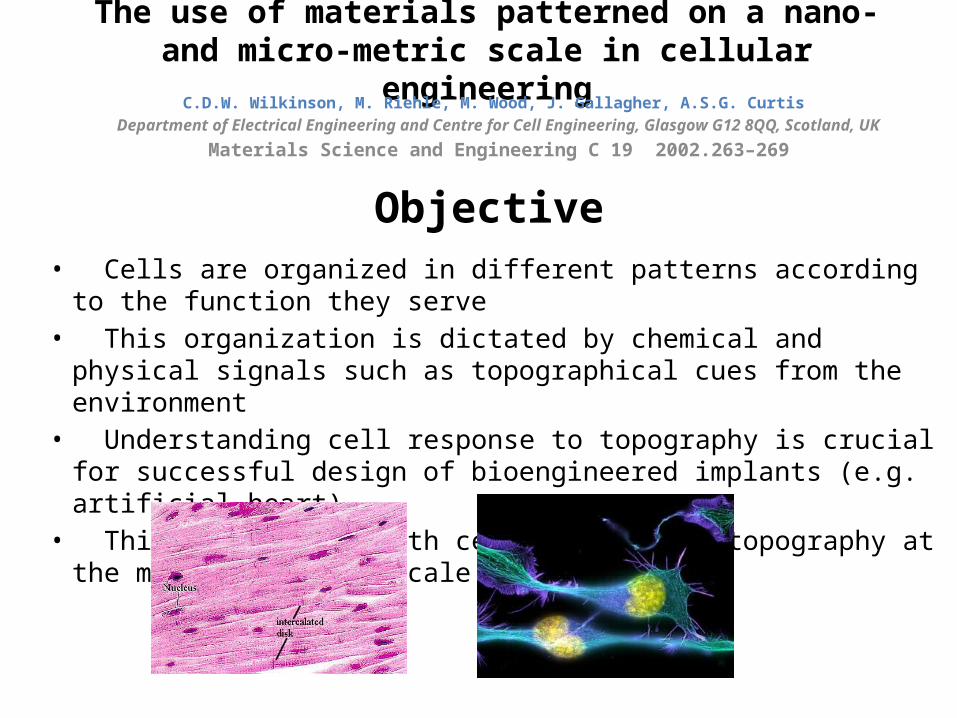
• Cells are organized in different patterns according to the function they serve• This organization is dictated by chemical and physical signals such as
topographical cues from the environment• Understanding cell response to topography is crucial for successful design of
bioengineered implants (e.g. artificial heart)• This paper deals with cell response to topography at the micro- and nano-scale
Objective
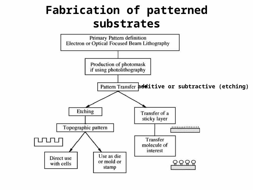
Fabrication of patterned substrates
additive or subtractive (etching)
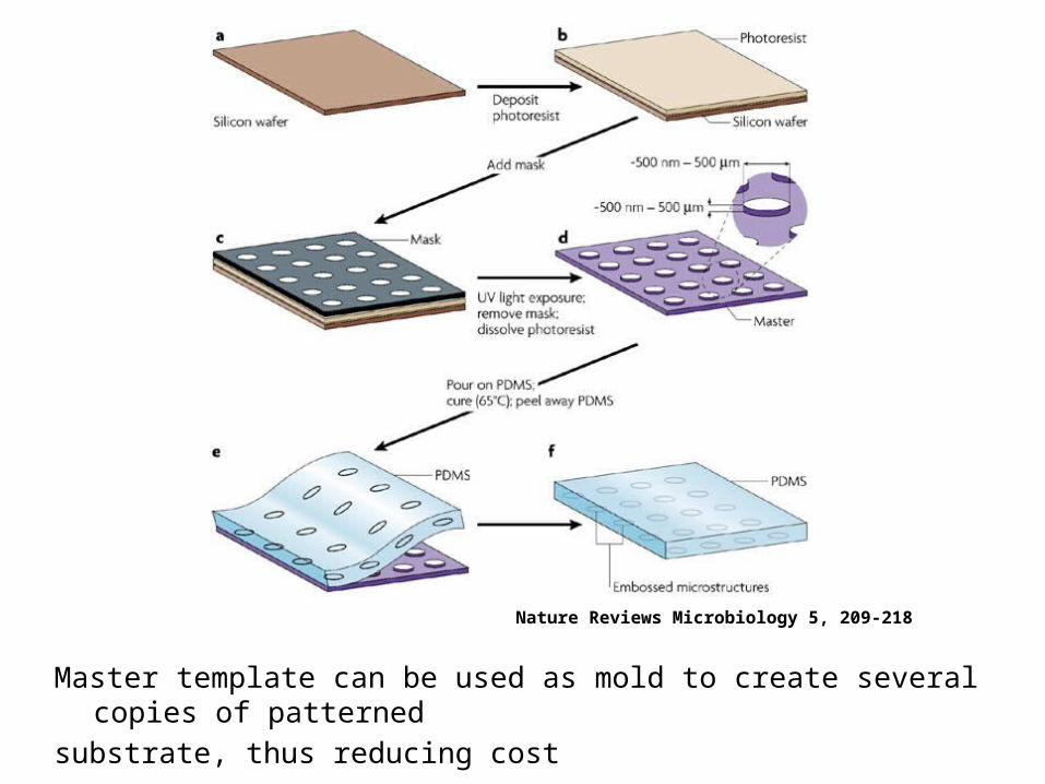
Master template can be used as mold to create several copies of patterned substrate, thus reducing cost
Nature Reviews Microbiology 5, 209-218
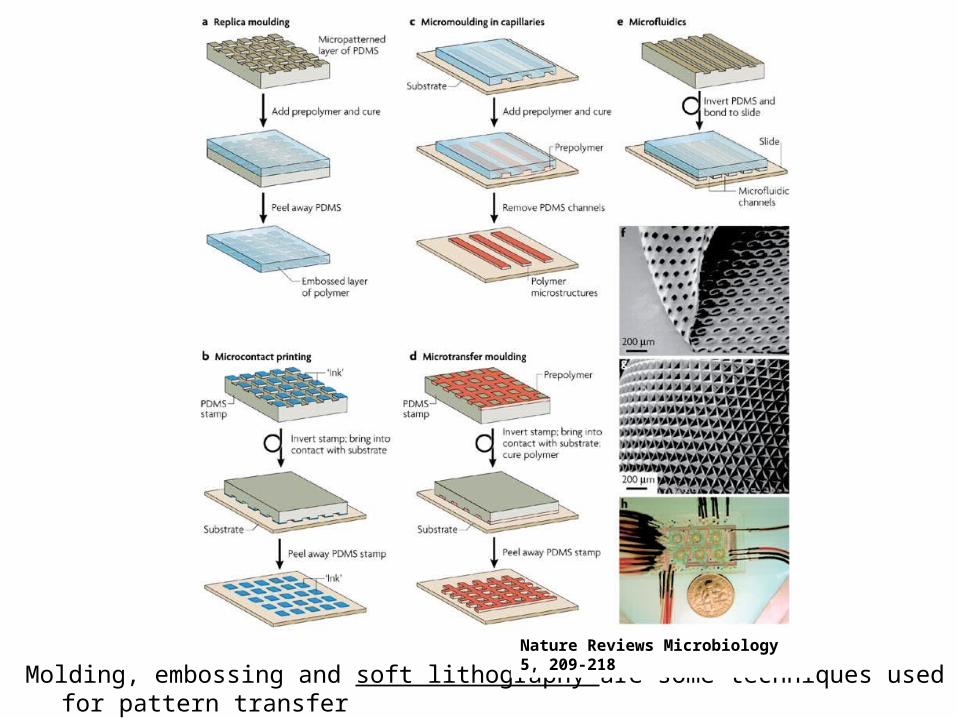
Molding, embossing and soft lithography are some techniques used for pattern transferNature Reviews Microbiology 5, 209-218
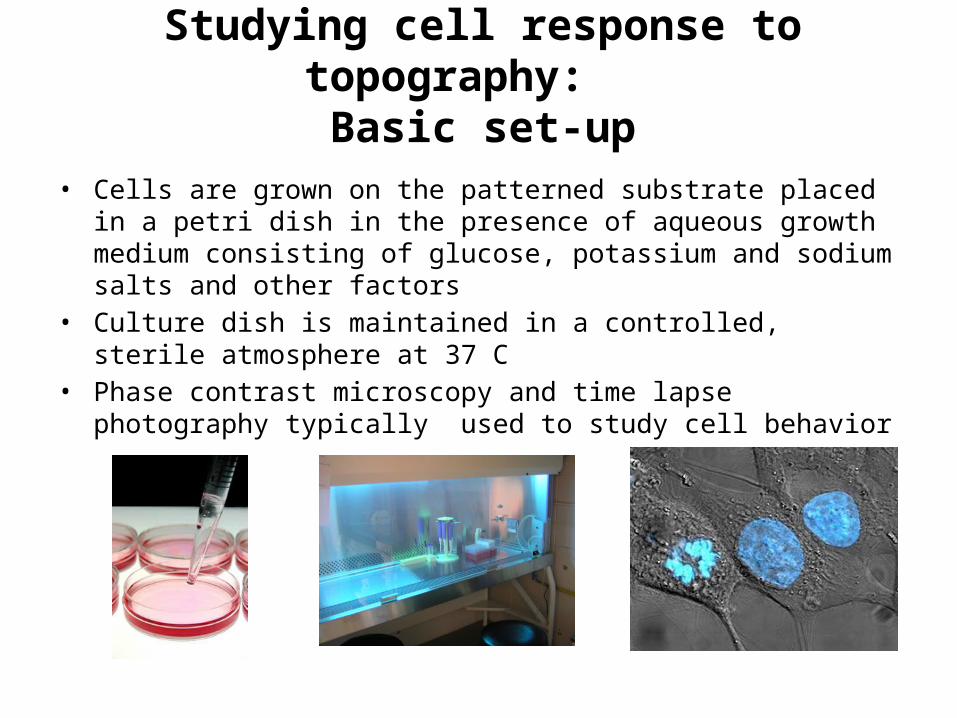
Studying cell response to topography: Basic set-up
• Cells are grown on the patterned substrate placed in a petri dish in the presence of aqueous growth medium consisting of glucose, potassium and sodium salts and other factors
• Culture dish is maintained in a controlled, sterile atmosphere at 37 C• Phase contrast microscopy and time lapse photography typically used to
study cell behavior
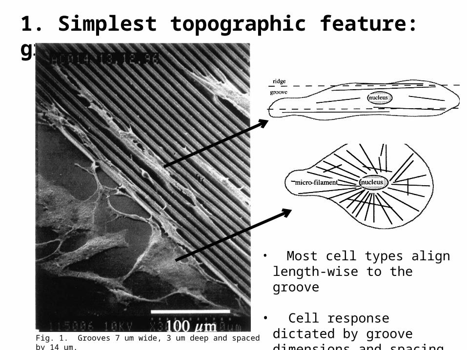
1. Simplest topographic feature: grooves
• Most cell types align length-wise to the groove
• Cell response dictated by groove dimensions and spacing
Fig. 1. Grooves 7 um wide, 3 um deep and spaced by 14 um.
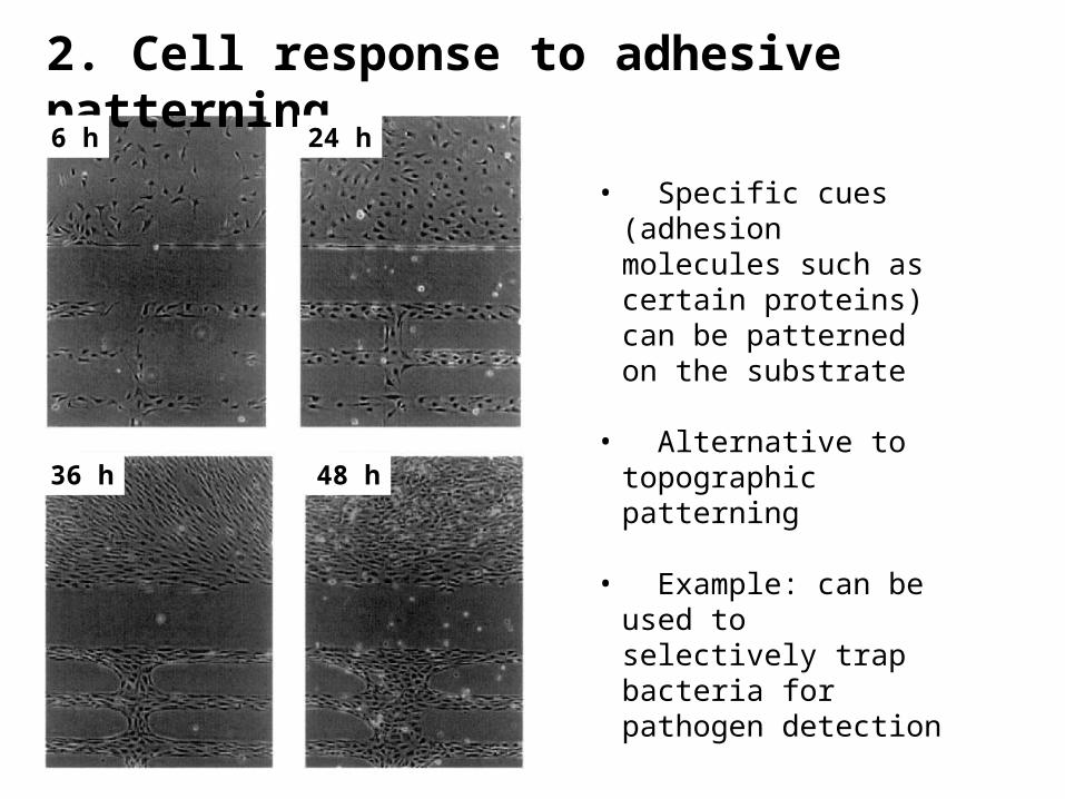
2. Cell response to adhesive patterning
• Specific cues (adhesion molecules such as certain proteins) can be patterned on the substrate
• Alternative to topographic patterning
• Example: can be used to selectively trap bacteria for pathogen detection
6 h 24 h
48 h36 h
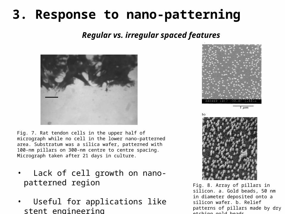
3. Response to nano-patterning
Fig. 7. Rat tendon cells in the upper half of micrograph while no cell in the lower nano-patterned area. Substratum was a silica wafer, patterned with 100-nm pillars on 300-nm centre to centre spacing.Micrograph taken after 21 days in culture.
Fig. 8. Array of pillars in silicon. a. Gold beads, 50 nm in diameter deposited onto a silicon wafer. b. Relief patterns of pillars made by dry etching gold beads
Regular vs. irregular spaced features
• Lack of cell growth on nano-patterned region
• Useful for applications like stent engineering
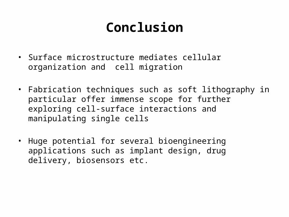
Conclusion
• Surface microstructure mediates cellular organization and cell migration
• Fabrication techniques such as soft lithography in particular offer immense scope for further exploring cell-surface interactions and manipulating single cells
• Huge potential for several bioengineering applications such as implant design, drug delivery, biosensors etc.


![Apparato Stomatognatico (A.S.G.): Apparato Masticatorio (A.M.) · Microsoft PowerPoint - Lezione 12. ATM.ppt [modalità compatibilità] Created Date: 20181128114027Z](https://img.pdfslide.net/doc/110x75/5f1d4617a2ce674ea90aa642/apparato-stomatognatico-asg-apparato-masticatorio-am-microsoft-powerpoint.jpg)