Embed Size (px)
Citation preview
Copyright © 2017 Silex Microsystems. All rights reserved. SILEX CONFIDENTIAL
The World’s Leading Pure Play MEMS Foundry
Copyright © 2017 Silex Microsystems. All rights reserved. SILEX CONFIDENTIAL
THE WORLD´S LEADING PURE-PLAY MEMS FOUNDRY
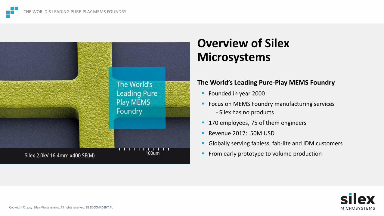
Overview of SilexMicrosystems
The World’s Leading Pure-Play MEMS Foundry
▪ Founded in year 2000
▪ Focus on MEMS Foundry manufacturing services
- Silex has no products
▪ 170 employees, 75 of them engineers
▪ Revenue 2017: 50M USD
▪ Globally serving fabless, fab-lite and IDM customers
▪ From early prototype to volume production
Copyright © 2017 Silex Microsystems. All rights reserved. SILEX CONFIDENTIAL
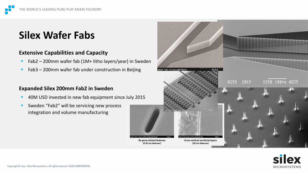
Extensive Capabilities and Capacity
▪ Fab2 – 200mm wafer fab (1M+ litho layers/year) in Sweden
▪ Fab3 – 200mm wafer fab under construction in Beijing
Expanded Silex 200mm Fab2 in Sweden
▪ 40M USD invested in new fab equipment since July 2015
▪ Sweden “Fab2” will be servicing new process
integration and volume manufacturing
THE WORLD´S LEADING PURE-PLAY MEMS FOUNDRY
Silex Wafer Fabs
Copyright © 2017 Silex Microsystems. All rights reserved. SILEX CONFIDENTIAL
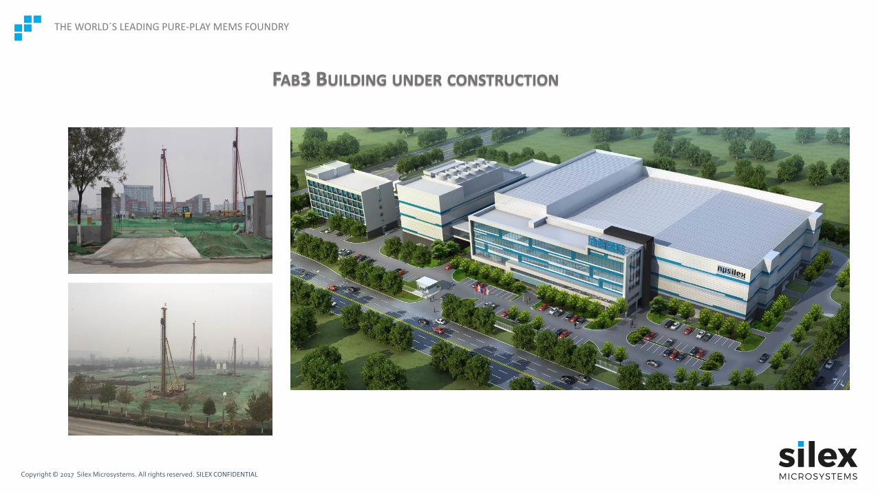
FAB3 BUILDING UNDER CONSTRUCTION
THE WORLD´S LEADING PURE-PLAY MEMS FOUNDRY
Copyright © 2017 Silex Microsystems. All rights reserved. SILEX CONFIDENTIAL
THE WORLD´S LEADING PURE-PLAY MEMS FOUNDRY
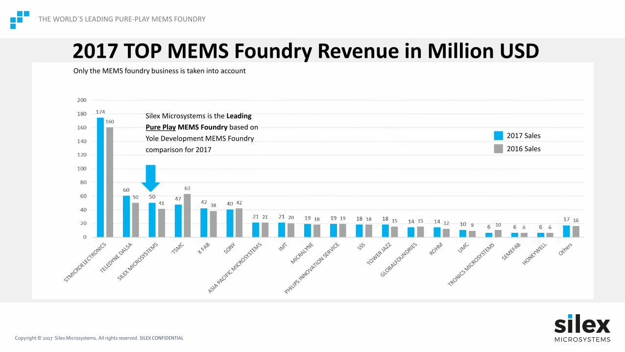
2017 TOP MEMS Foundry Revenue in Million USD
Silex Microsystems is the Leading
Pure Play MEMS Foundry based on
Yole Development MEMS Foundry
comparison for 2017
Only the MEMS foundry business is taken into account
2017 Sales
2016 Sales
Copyright © 2017 Silex Microsystems. All rights reserved. SILEX CONFIDENTIAL
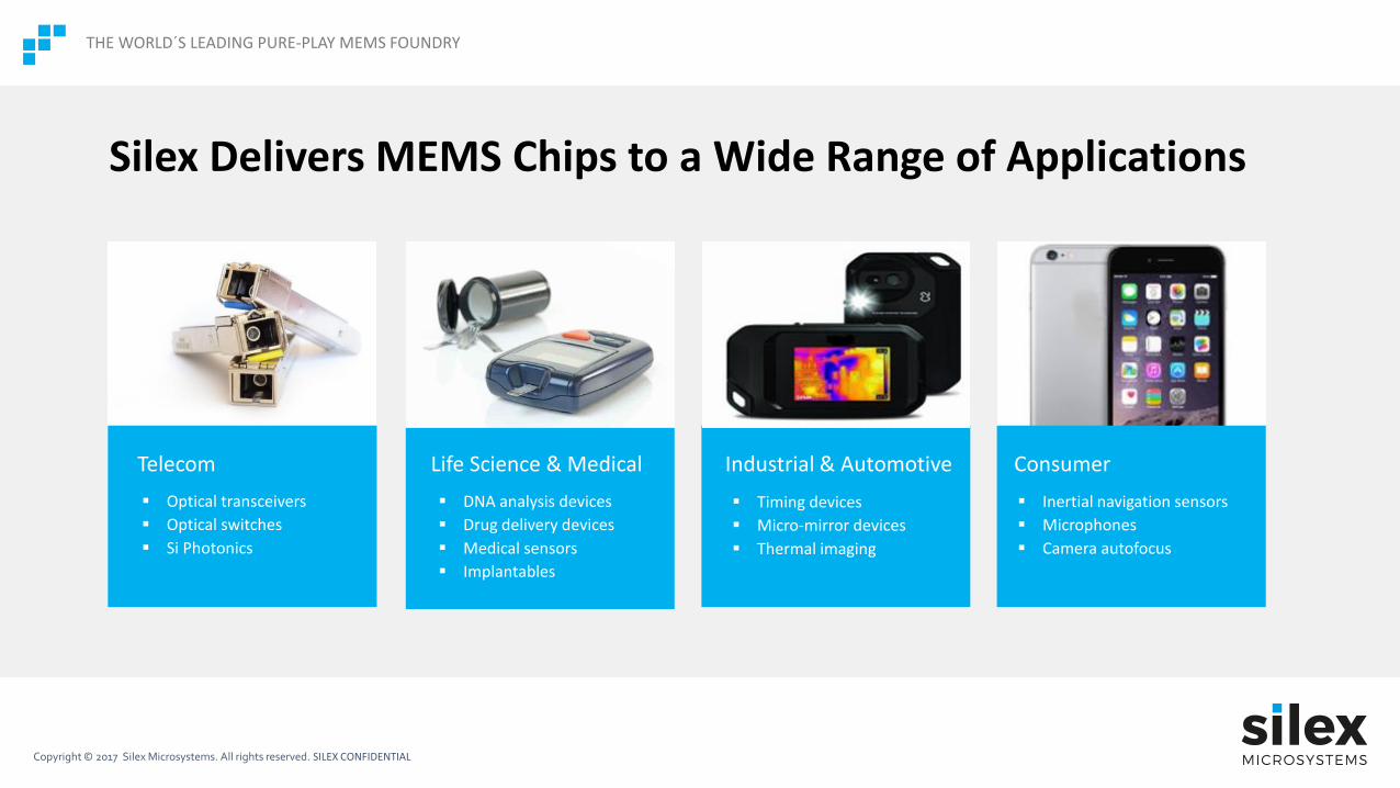
Silex Delivers MEMS Chips to a Wide Range of Applications
THE WORLD´S LEADING PURE-PLAY MEMS FOUNDRY
▪ DNA analysis devices
▪ Drug delivery devices
▪ Medical sensors
▪ Implantables
Life Science & MedicalTelecom
▪ Optical transceivers
▪ Optical switches
▪ Si Photonics
Industrial & Automotive
▪ Timing devices
▪ Micro-mirror devices
▪ Thermal imaging
Consumer
▪ Inertial navigation sensors
▪ Microphones
▪ Camera autofocus
Copyright © 2017 Silex Microsystems. All rights reserved. SILEX CONFIDENTIAL
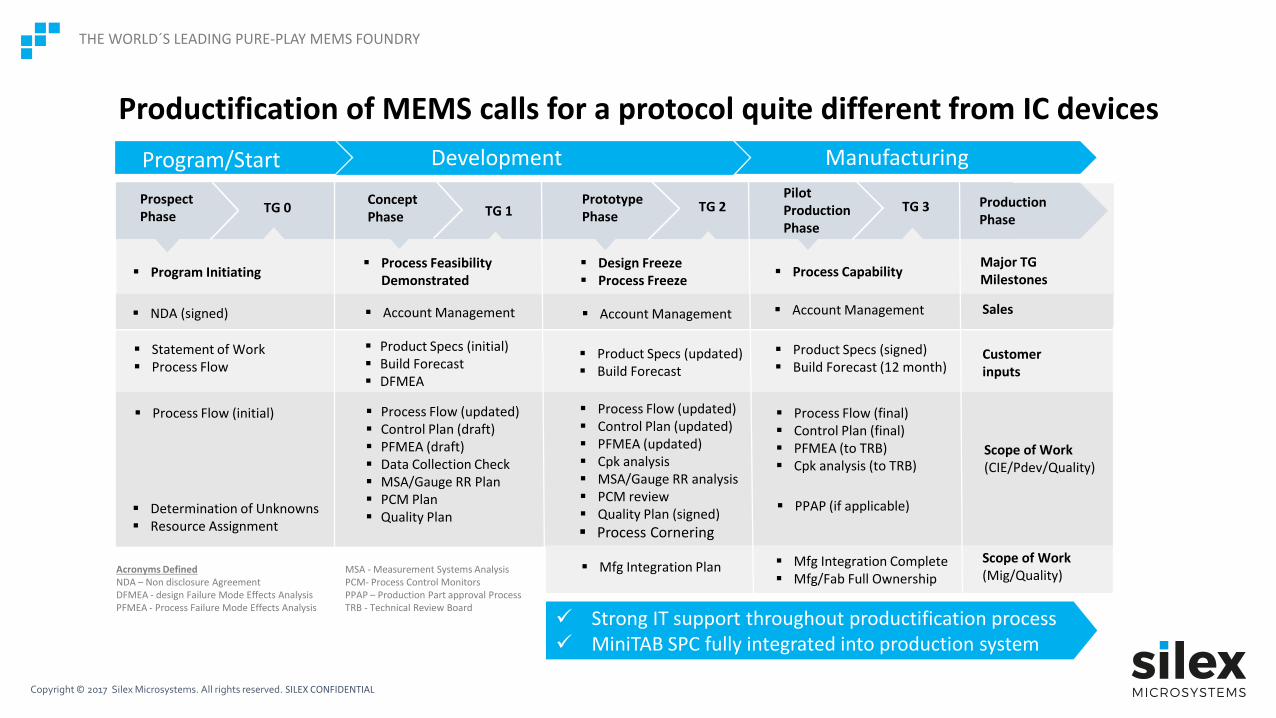
Acronyms DefinedNDA – Non disclosure AgreementDFMEA - design Failure Mode Effects AnalysisPFMEA - Process Failure Mode Effects Analysis
MSA - Measurement Systems AnalysisPCM- Process Control MonitorsPPAP – Production Part approval ProcessTRB - Technical Review Board
THE WORLD´S LEADING PURE-PLAY MEMS FOUNDRY
TG 0
▪ Process Flow (initial)
TG 1
▪ Process FeasibilityDemonstrated
▪ Design Freeze▪ Process Freeze
▪ Process Capability
TG 2 TG 3
Major TGMilestones
▪ Program Initiating
▪ Statement of Work▪ Process Flow
▪ Product Specs (initial)▪ Build Forecast▪ DFMEA
▪ Process Flow (updated)▪ Control Plan (draft)▪ PFMEA (draft)▪ Data Collection Check▪ MSA/Gauge RR Plan▪ PCM Plan▪ Quality Plan
▪ Process Flow (updated)▪ Control Plan (updated)▪ PFMEA (updated) ▪ Cpk analysis▪ MSA/Gauge RR analysis▪ PCM review▪ Quality Plan (signed)
▪ Product Specs (updated)▪ Build Forecast
▪ Process Flow (final)▪ Control Plan (final)▪ PFMEA (to TRB)▪ Cpk analysis (to TRB)
Customerinputs
ProspectPhase
ConceptPhase
PrototypePhase
ProductionPhase
ManufacturingDevelopmentProgram/Start
▪ Determination of Unknowns▪ Resource Assignment
▪ NDA (signed) ▪ Account Management ▪ Account Management ▪ Account Management Sales
Scope of Work(CIE/Pdev/Quality)
▪ Product Specs (signed)▪ Build Forecast (12 month)
▪ PPAP (if applicable)
Pilot ProductionPhase
▪ Process Cornering
▪ Mfg Integration Complete▪ Mfg/Fab Full Ownership
Scope of Work(Mig/Quality)
▪ Mfg Integration Plan
Productification of MEMS calls for a protocol quite different from IC devices
✓ Strong IT support throughout productification process✓ MiniTAB SPC fully integrated into production system
Copyright © 2017 Silex Microsystems. All rights reserved. SILEX CONFIDENTIAL
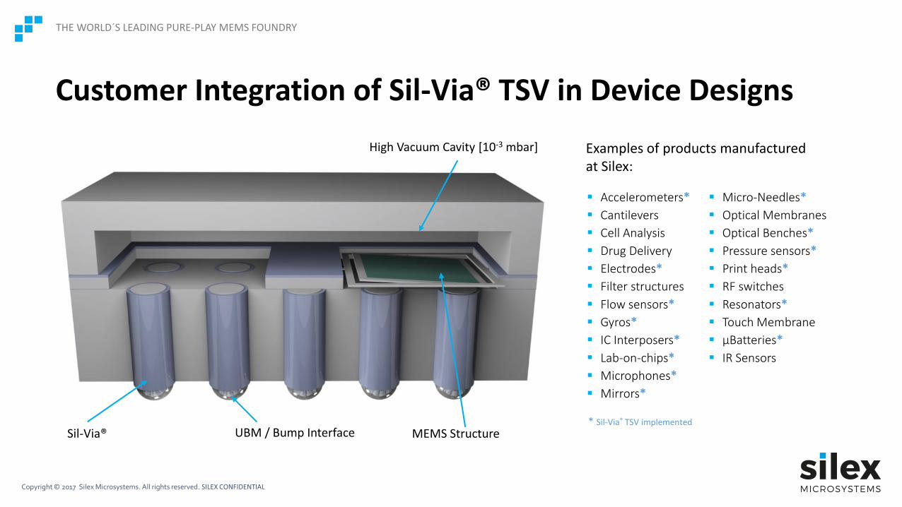
High Vacuum Cavity [10-3 mbar]
Sil-Via® UBM / Bump Interface MEMS Structure
▪ Accelerometers*
▪ Cantilevers
▪ Cell Analysis
▪ Drug Delivery
▪ Electrodes*
▪ Filter structures
▪ Flow sensors*
▪ Gyros*
▪ IC Interposers*
▪ Lab-on-chips*
▪ Microphones*
▪ Mirrors*
▪ Micro-Needles*
▪ Optical Membranes
▪ Optical Benches*
▪ Pressure sensors*
▪ Print heads*
▪ RF switches
▪ Resonators*
▪ Touch Membrane
▪ µBatteries*
▪ IR Sensors
Examples of products manufactured at Silex:
* Sil-Via® TSV implemented
Customer Integration of Sil-Via® TSV in Device Designs
THE WORLD´S LEADING PURE-PLAY MEMS FOUNDRY
Copyright © 2017 Silex Microsystems. All rights reserved. SILEX CONFIDENTIAL
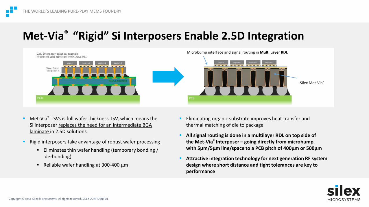
▪ Met-Via® TSVs is full wafer thickness TSV, which means the Si interposer replaces the need for an intermediate BGA laminate in 2.5D solutions
▪ Rigid interposers take advantage of robust wafer processing
▪ Eliminates thin wafer handling (temporary bonding /de-bonding)
▪ Reliable wafer handling at 300-400 µm
▪ Eliminating organic substrate improves heat transfer and thermal matching of die to package
▪ All signal routing is done in a multilayer RDL on top side of the Met-Via® Interposer – going directly from microbumpwith 5µm/5µm line/space to a PCB pitch of 400µm or 500µm
▪ Attractive integration technology for next generation RF system design where short distance and tight tolerances are key toperformance
Met-Via® “Rigid” Si Interposers Enable 2.5D Integration
THE WORLD´S LEADING PURE-PLAY MEMS FOUNDRY
Microbump interface and signal routing in Multi Layer RDL
Silex Met-Via®
Copyright © 2017 Silex Microsystems. All rights reserved. SILEX CONFIDENTIAL
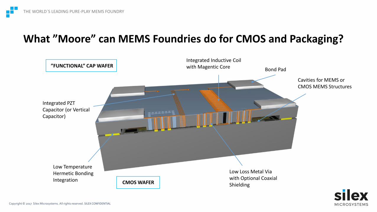
What ”Moore” can MEMS Foundries do for CMOS and Packaging?
THE WORLD´S LEADING PURE-PLAY MEMS FOUNDRY
”FUNCTIONAL” CAP WAFER
Integrated PZT Capacitor (or VerticalCapacitor)
Bond Pad
Integrated Inductive Coilwith Magentic Core
Low TemperatureHermetic Bonding Integration
Low Loss Metal Via with Optional CoaxialShielding
Cavities for MEMS or CMOS MEMS Structures
CMOS WAFER

Copyright © 2017 Silex Microsystems. All rights reserved. SILEX CONFIDENTIAL
Thank You