Embed Size (px)
Citation preview

www.epc-co.comEPC - The Leader in eGaN® FETs 11
The eGaN® FET Journey Continues
Efficient Power Conversion Corporation
The ZVS Class-D Amplifier, an eGaN®
FET-enabled Topology for Highly Resonant Wireless Power Transfer

www.epc-co.comEPC - The Leader in eGaN® FETs 2
Agenda
• Introduction to the A4WP Class-3 Specifications
• ZVS Class D Amplifier• eGaN® FET versus MOSFET Comparison• Testing to the A4WP Class-3 Specifications• Experimental Results• Summary
eGaN® is a registered trademark of Efficient Power Conversion Corporation
www.epc-co.comEPC - The Leader in eGaN® FETs 3
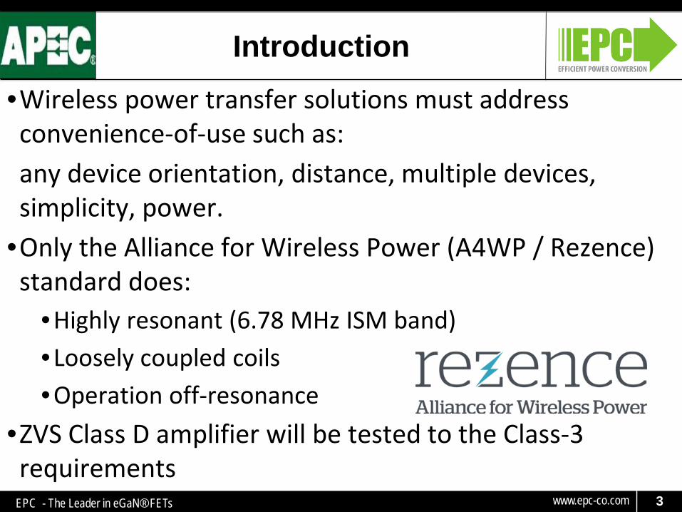
Introduction•Wireless power transfer solutions must address convenience-of-use such as:any device orientation, distance, multiple devices, simplicity, power.
•Only the Alliance for Wireless Power (A4WP / Rezence) standard does:
•Highly resonant (6.78 MHz ISM band)•Loosely coupled coils•Operation off-resonance
•ZVS Class D amplifier will be tested to the Class-3 requirements

www.epc-co.comEPC - The Leader in eGaN® FETs 4
A4WP Class-3 Impedance Requirements
Unloaded Coil Arc
Full Load Arc
Load Variation
Arcs
Decreasing Capacitance
Increasing Inductance
50 ΩSmithChart
On Resonance
1 +10j Ω
1 -150j Ω
55 +10j Ω
55 -150j ΩMatched Coil
Impedance Rotation permissible

www.epc-co.comEPC - The Leader in eGaN® FETs 5
Class-3 Coil Drive Requirements
0
20
40
60
80
100
120
140
0 10 20 30 40 50 60
Coil
Volta
ge [V
]
Real Reflected Resistance [Ω]
10j [Ω]0j [Ω]20j [Ω]40j [Ω]80j [Ω]150j [Ω]
800 mA Region
Power Limit 16 W
Amplifier LimitedVector sum of real (R) and imaginary (X) impedance range

www.epc-co.comEPC - The Leader in eGaN® FETs 6
ZVS Class D Amplifier
V / I
VDS ID
time
VDD
50%Ideal Waveforms
ILZVS
• Switch voltage rating = Supply (VDD).• COSS Voltage is transitioned by the ZVS tank • ZVS tank circuit does not carry load current• Coil Voltage = (√2/π)·VDD [VRMS]
+VDD
CsQ2
Q1 Zload
LZVS
CZVS
ZVS tank

www.epc-co.comEPC - The Leader in eGaN® FETs 7
Ultra High FrequencyeGaN FETs
Drain
Source
Gate Substrate (Connect to Source on PWB)
Solder side View
Part Number Package (mm)
VDS (V)
VGS (V)
RDS(on)@5 V (mΩ)
QG @5 V Typ. (pC)
QGSTyp. (pC)
QGDTyp. (pC)
RGTyp. (Ω)
VthTyp. (V)
QRR(nC)
ID(A)
TJ Max. (˚C)
EPC8004 LGA 2.05x0.85 40 6 125 358 110 31 0.34 1.4 0 2.7 150
EPC8009 LGA 2.05x0.85 65 6 138 380 116 36 0.3 1.4 0 2.7 150
EPC8010 LGA 2.05x0.85 100 6 160 354 109 32 0.3 1.4 0 2.7 150
2.05 x 0.85 mm
Gate Return
• Proven in various wireless power transfer amplifiers• Low CISS• Low COSS• Zero QRR• Full dv/dt immunity
www.epc-co.comEPC - The Leader in eGaN® FETs 8
0100200300400500600700
EPC8010 MOSFET 2
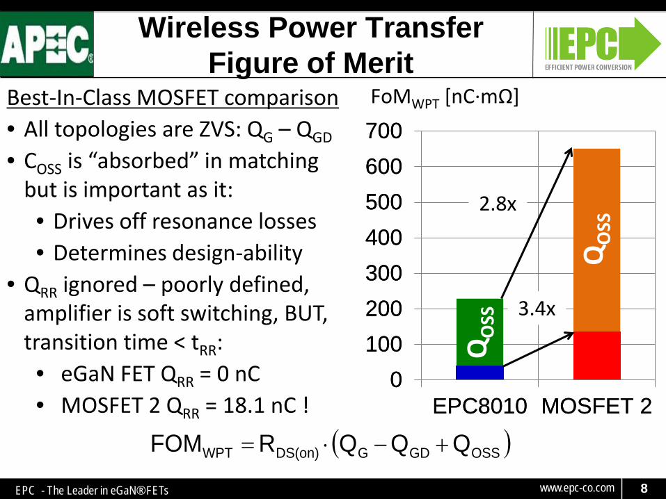
Wireless Power Transfer Figure of Merit
( )OSSGDGDS(on)WPT QQQRFOM +−⋅=
FoMWPT [nC·mΩ]Best-In-Class MOSFET comparison• All topologies are ZVS: QG – QGD
• COSS is “absorbed” in matching but is important as it:• Drives off resonance losses• Determines design-ability
• QRR ignored – poorly defined, amplifier is soft switching, BUT, transition time < tRR:• eGaN FET QRR = 0 nC• MOSFET 2 QRR = 18.1 nC !
0100200300400500600700
EPC8010 MOSFET 2
3.4x
2.8x
QO
SS
QO
SS

www.epc-co.comEPC - The Leader in eGaN® FETs 9
Experimental Amplifier
eGaN FET EPC8010125 mΩ
Load Connection
Gate Driver LM5113 (5 V)
ZVS Capacitor CZVS
MOSFET 2105 mΩ
Load Connection
ZVS Inductor LZVSOscilloscope Probe Holder

www.epc-co.comEPC - The Leader in eGaN® FETs 10
Load Variation (Ω) Results
1357911131517
808284868890929496
0 10 20 30 40 50 60
Out
put P
ower
[W]
Effic
ienc
y [%
]
Real Reflected Resistance [Ω]
Total Amplifier Efficiency
EPC8010 0j ΩMOSFET 0j Ω
Pout
808284868890929496
0 10 20 30 40 50 60
Effic
ienc
y [%
]
Real Reflected Resistance [Ω]
Total Amplifier Efficiency
EPC8010 -30j ΩMOSFET -30j Ω
808284868890929496
0 10 20 30 40 50 60
Effic
ienc
y [%
]
Real Reflected Resistance [Ω]
Total Amplifier Efficiency
EPC8010 +20j ΩMOSFET +20j Ω

www.epc-co.comEPC - The Leader in eGaN® FETs 11
00.5
11.5
22.5
33.5
-30 -25 -20 -15 -10 -5 0 5 10 15 20
Pow
er [W
]
Imaginary Impedance [jΩ]
Total Amplifier Losses
00.5
11.5
22.5
33.5
-30 -25 -20 -15 -10 -5 0 5 10 15 20
Pow
er [W
]
Imaginary Impedance [jΩ]
Total Amplifier Losses
00.5
11.5
22.5
33.5
-30 -25 -20 -15 -10 -5 0 5 10 15 20
Pow
er [W
]
Imaginary Impedance [jΩ]
Total Amplifier Losses
Load Variation (jΩ) Results
5 % lower
MOSFET 10 Ω 7 WEPC8010 10 Ω 7 W
20 % lower
MOSFET 36 Ω 16 WEPC8010 36 Ω 16 W
30 % lower
MOSFET 55 Ω 16 WEPC8010 55 Ω 16 W

www.epc-co.comEPC - The Leader in eGaN® FETs 12
Summary
eGaN FETs in a ZVS Class D amplifier were tested to the A4WP Class-3 specifications :
• eGaN FETs always yield higher efficiency than best-in-class MOSFETs
• Gate driver and eGaN FET temperature remain below 100˚C
• eGaN FET’s lower COSS reduces the ZVS current needed, resulting in lower power dissipation for both FET and LZVS
• eGaN FETs reduce board space by 40 %

www.epc-co.comEPC - The Leader in eGaN® FETs 13
Wireless Power Handbook
• Visit EPC’s Booth #1405 to see several demonstrations in operation
• Handbook on wireless power that covers this work and much more – available at Digikey

www.epc-co.comEPC - The Leader in eGaN® FETs 1414
Thank You