Embed Size (px)
Citation preview
Theoretical Investigation of a new OFDM
Access-Network Topology (OTONES)
ADITYA KAKKAR
Degree project in
Photonics
Second cycle
Stockholm, Sweden 2013

Theoretical Investigation of a new OFDM
Access-Network Topology (OTONES)
Aditya Kakkar
Master of Science Thesis
European Master of Research on Information and Communication Technologies with specialization in Photonics
(Erasmus Mundus MERIT Program)
External Supervisor: Prof. Jürg Leuthold, KIT Karlsruhe, ETH Zürich External Cosupervisor: Philipp Schindler, KIT Karlsruhe
KTH Supervisor: Dr. Richard Schatz
KTH Examiner: Prof. Urban Westergren
KTH, Royal Institute of Technology Stockholm 2013
TRITA-ICT-EX-2013:162

i
Table of Contents Table of Contents ................................................................................................................... i
Abstract ................................................................................................................................ iii
Acknowledgement ..................................................................................................................v
1 Introduction .....................................................................................................................1
2 Fundamentals Behind OTONES topology ........................................................................4 2.1 Basics of Orthogonal Frequency Division Multiplexing (OFDM) with QAM Modulation ........................................................................................................................4
2.1.1 Quadrature Amplitude Modulation (QAM) ........................................................4 2.1.2 Multi-carrier data transmission ...........................................................................7 2.1.3 Sub-carrier generation using IFFT ......................................................................7
2.2 Optical Coherent Detection .......................................................................................9 2.2.1 Optical Hybrid and Balanced Photo detection .................................................. 10 2.2.2 General Block Diagram of Coherent Detection................................................. 12
2.3 Basics of Optical Modulators .................................................................................. 14 2.3.1 The MZI Modulator ......................................................................................... 14 2.3.2 IQ Modulator ................................................................................................... 16
2.4 Basics of Wavelength Division Multiplexing (WDM) ............................................. 18 2.4.1 WDM Parameters............................................................................................. 19
3 Single Side Band Modulation Techniques for Image Rejection ...................................... 22 3.1 Motivation .............................................................................................................. 22
3.1.1 Mathematical Background of Generation of Image Spectrum ........................... 23 3.2 Formulation of Requirements as per OTONES........................................................ 24 3.3 Methods for Generation of SSB/ Image Rejection ................................................... 25
3.3.1 Filtering Methods ............................................................................................. 25 3.3.2 Hilbert Transform Method ............................................................................... 27 3.3.3 Hartley Phasing Circuit Method ....................................................................... 29 3.3.4 Novel Bedrosian Method.................................................................................. 30 3.3.5 Weaver’s Method ............................................................................................. 32
3.4 Results and Discussion............................................................................................ 34 3.4.1 Tolerance Limits for Novel Bedrosian Method ................................................. 36
3.5 Conclusions ............................................................................................................ 41
4 Circuital Modeling of the OTONES Topology ............................................................... 43 4.1 OFDM Transmitter ................................................................................................. 45 4.2 OFDM Receiver ..................................................................................................... 46 4.3 Up-conversion Circuit with Pilot Tone Inclusion..................................................... 47
4.3.1 Electrical Amplifier Model............................................................................... 47 4.3.2 Mixer Model .................................................................................................... 48
4.4 SSB up-conversion Module..................................................................................... 49 4.5 Down-conversion Module ....................................................................................... 49 4.6 Remote Hub based WDM system............................................................................ 50
ii
4.7 IQ Optical Modulator Module ................................................................................. 51 4.7.1 MZM Modulator Module ................................................................................. 52 4.7.2 Phase Modulator Module ................................................................................. 52
4.8 Optical Amplifier Module ....................................................................................... 52
5 Results and Discussion .................................................................................................. 54
6 Conclusion and Outlook ................................................................................................ 61
Bibliography......................................................................................................................... 63
Appendix: List of Abbreviations ........................................................................................... 65
iii
Abstract Recent studies on growth of telecomm sector depict an ever rising demand for high bandwidth applications such as on-line gaming, high definition television and many more. This demand is coupled with increase in internet connected utilities per house hold - each requiring a portion of bandwidth. The fast development of broadband telecommunication services calls for an upgrade of access infrastructure. This challenge could be met by technologies such as Fiber-To-The-Home/Building (FTTH/B) point-to-multipoint (P2MP) optical access networking. Further, FTTH is also widely regarded as a future proof solution for broadband telecommunication services within scientific and industrial sectors. This has encouraged large amount of research and development throughout the globe to find optimal topologies for FTTH.
OFDM based optical access network topology abbreviated as OTONES is an ongoing EU FP 7 project under the PIANO+ framework. The OTONES project addresses the next generation optical access networking on the basis of Orthogonal Frequency Division Multiplexing (OFDM) and Orthogonal Frequency Multiple Access (OFDMA), with special provision for reduced complexity and signal processing aspects of the subscriber side terminals (ONUs).
This thesis focuses on the theoretical investigation of OFDM based optical access network topology OTONES. The thesis provides an in depth view of the salient aspects of the topology and formulates the key requirements of OTONES topology. The investigation primarily delves on two important aspects of the topology. First, finding the optimal analog circuitry for the optical network unit (ONU). Second, finding the optimal operation regime for the topology and hence optimizing the system level concept.
In this thesis, we show that the requirement of an analog circuitry originates from the need of successive up-conversions in OTONES topology which also produces image spectrum. This image spectrum causes a 3 dB loss in power and spectral efficiency in absence of a proper image rejection circuitry. Thus, we discuss the generic SSB generation methods for efficient image rejection. Novel Bedrosian method based on Bedrosian Theorem is established as a promising method for image rejection. We show that this method is an analog implementation of Hilbert Transform Method and does not involve any approximation. Both generic methods for SSB along with the Novel Bedrosian method are evaluated based on the criterion established for OTONES topology. Finally, optical filtering from the set of generic SSB method is proposed for the downstream path and Novel Bedrosian method is proposed for the upstream path. The tolerance limits for Novel Bedrosian method, are also established for its physical implementation.
We further discuss the realistic implementation of various components of the OTONES topology. We also establish the optimal operation regime of the full concurrent topology based on parameters such as input optical power, pilot tone separation and many more.
iv
Finally as a key feature of the thesis, we optimize the system level concept of the topology with the use of the proposed Novel Bedrosian Method as the optimal analog circuitry for OTONES topology and provide a region of optimal operation of the topology.
KEYWORDS: OTONES, SSB Method, Image Rejection, Novel Bedrosian Method,
Orthogonal Frequency Division Multiplexing (OFDM), Optical Network Unit (ONU), Optical Line Terminal (OLT), Coherent Receiver, Remote Heterodyne Detection, Optical Access Network, WDM network.
v
Acknowledgement I would like to express my sincere gratitude to my advisor, Prof. Dr. Jürg Leuthold, for his unmatched guidance and support throughout the course of my thesis. He was kind enough to give me the opportunity to join his research group and has been a source of inspiration and motivation for me since then. He has helped me to comprehend the field of photonics and optical communication and untangle the complexities of this field. He always finds time for his students in his busy schedule. This thesis would not be possible without his continuous guidance and support. His immense knowledge of this field has made my research work an enjoyable and learning experience.
This research was done as part of my master thesis at KTH, Sweden. I extend my heartfelt gratitude to my thesis examiner Prof. Urban Westergren, for his valuable guidance and support throughout the thesis. This has turned out to be a golden opportunity which has helped to grow both professionally and personally. I am deeply thankful to my supervisors at KTH Sweden, Dr. Richard Schatz for his support and guidance throughout the work.
I wish to thank my supervisor Philipp Schindler for his insightful discussions and kind help on questions related to many areas. The thesis required a lot of data and Philipp has always been very cooperative and agile in providing it. He always has an eye to details which has helped me to address even the minor issues in my work. His quick insights to the technical problems in the implementation are highly recommendable. His guidance has kept me motivated and their contribution to this work is unmatched and unparalleled.
Most importantly, I would like to thank my father C. A. Surendra Kakkar, my mother Rachna Kakkar and my loving sister Devika Kakkar for their countless blessings and unwavering support all the time. Without their unconditional love and support, nothing could have been possible. Finally, I thank the Almighty for giving me this opportunity and strength needed to work on this thesis.
1
1 Introduction Users of telecommunication access networks are nowadays showing interest in high-bandwidth applications such as on-line gaming, video telephony, video-on-demand, high-definition television and peer-to-peer applications. Moreover, many households have multiple personal computers connected to internet - each requiring a portion of bandwidth. The fast development of broadband telecommunication services requires an upgrade of access infrastructure. This challenge could be met by technologies such as Fiber-To-The-Home/Building (FTTH/B) point-to-multipoint (P2MP) optical access networking.
In addition, FTTH is widely regarded as a future proof solution for broadband telecommunication services within scientific and industrial sectors. This has encouraged large amount of research and development throughout the globe to find optimal topologies for FTTH.
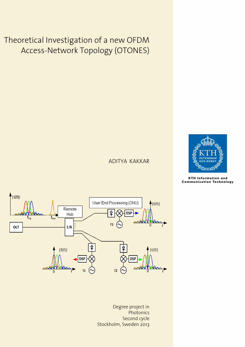
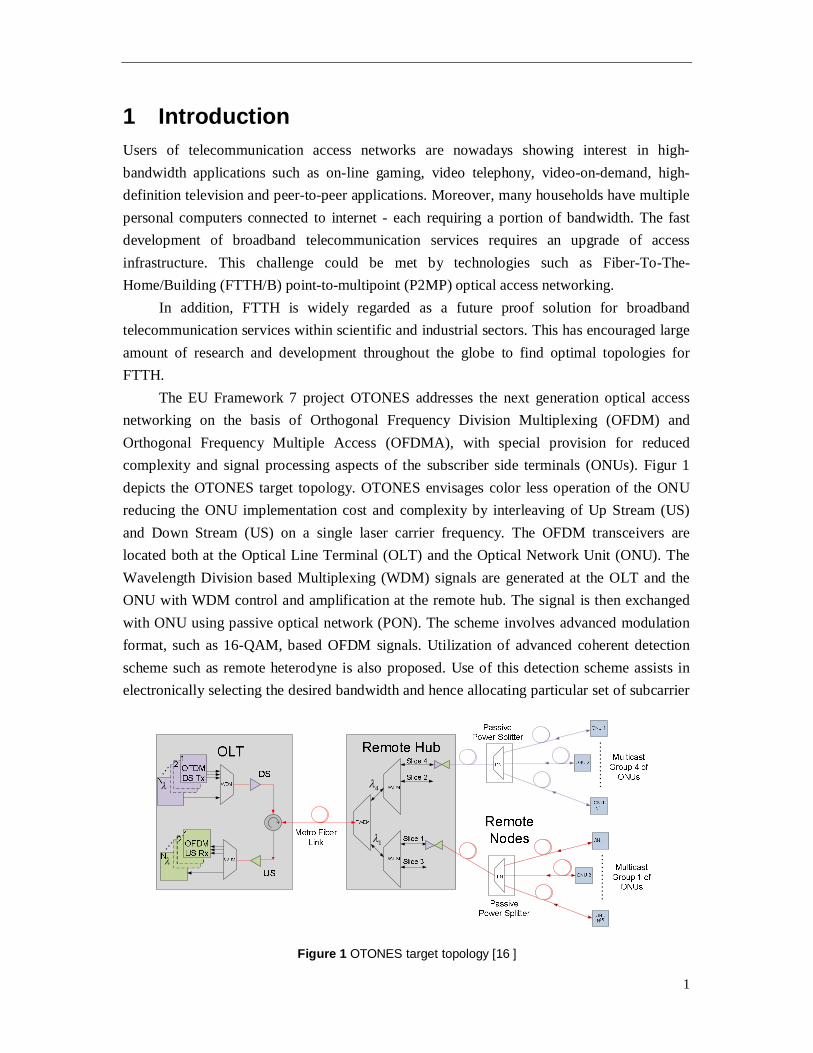
The EU Framework 7 project OTONES addresses the next generation optical access networking on the basis of Orthogonal Frequency Division Multiplexing (OFDM) and Orthogonal Frequency Multiple Access (OFDMA), with special provision for reduced complexity and signal processing aspects of the subscriber side terminals (ONUs). Figur 1 depicts the OTONES target topology. OTONES envisages color less operation of the ONU reducing the ONU implementation cost and complexity by interleaving of Up Stream (US) and Down Stream (US) on a single laser carrier frequency. The OFDM transceivers are located both at the Optical Line Terminal (OLT) and the Optical Network Unit (ONU). The Wavelength Division based Multiplexing (WDM) signals are generated at the OLT and the ONU with WDM control and amplification at the remote hub. The signal is then exchanged with ONU using passive optical network (PON). The scheme involves advanced modulation format, such as 16-QAM, based OFDM signals. Utilization of advanced coherent detection scheme such as remote heterodyne is also proposed. Use of this detection scheme assists in electronically selecting the desired bandwidth and hence allocating particular set of subcarrier
4
1
Figure 1 OTONES target topology [16 ]
2
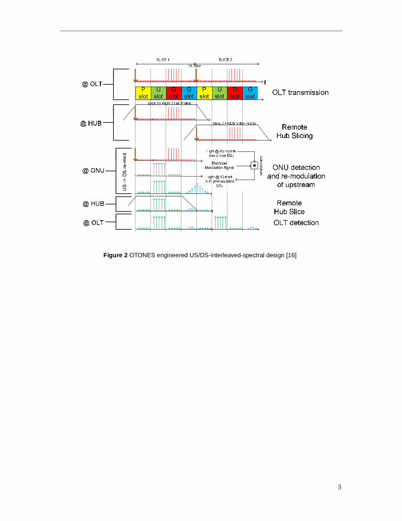
to each ONU user. This scheme acts a bridge between 25 GHz wide band communication band at the metro layer and low bandwidth signal processing at the ONU.
The evolution of the spectral components along the DS and US transmission chain is depicted in Figure 2. Each slice at the OLT is 12.5 GHz wide encompassing the up-converted DS OFDM signal along with the pilot tone. The slices are combined to form 25 GHz wide signal. 25 GHz aggregate signal is modulated on an optical carrier and transmitted along with other WDM signals on a single trunk fiber. The 25 GHz spectra is split back in the remote hub by FWDM to two 12.5 GHz slices to be multi-casted to respective groups using remote passive nodes. On reception in the ONU, detection and re-modulation of upstream on the U slot is carried out concurrently in the ONU. The convolution of electrical signal with the incoming DS spectra results in the desired signal and a spurious signal. The spurious signal is the outcome from the convolution of DS data spectrum and the US data spectrum. The 12.5 GHz bands are again combined in the remote hub to form 25 GHz band which is coherently detected in OLT. The circuital implementation of the scheme is discussed in detail in Chapter 4. The further details of the OTONES project and its feature can be found in the OTONES concept paper [16].
In this thesis, theoretical investigation of this novel Orthogonal Frequency Division Multiplexing (OFDM) based optical access network topology (OTONES) for FTTH as last mile solution is done. We investigate the possible analog circuitry to reduce the requirements for digital electronics: Optical Network Unit (ONU) Digital to Analog Converter (DAC)/ Analog to Digital Converter (ADC) rate reduction and improve overall energy and spectral efficiency. Further, we emulate the full concurrent network operation by deploying practical models for components encompassing noise and other imparities. Study of the effects of various system related parameters on the overall network performance is carried out. We theoretically optimize system level concept with respect to the cost and reach. Finally, we establish lower thresholds for operating points of components of both electrical and optical (E/O) domain and upper performance bound of the topology.
3
Figure 2 OTONES engineered US/DS-interleaved-spectral design [16]
4
2 Fundamentals Behind OTONES topology The novel OTONES topology envisions the utilization of various state of the art technologies such as OFDM, remote heterodyne detection and many more. In this chapter we discuss the underlying theory and basic principles behind those technologies. Details can as well be referred in [9] and [11].
2.1 Basics of Orthogonal Frequency Division Multiplexing (OFDM) with QAM Modulation
The basic principle behind OFDM is to sub-divide a high data rate stream into multiple lower data rate streams modulated on a number of closely spaced orthogonal subcarriers. The decrease in individual data rate results in decrease in dispersion in time caused by dispersive channels such as optical fibers. ODFM based design has an inherent capability to include a cyclically extended guard interval in every OFDM symbol. This cyclic guard interval assists in avoiding and eliminating inter-symbol interference and inter-carrier interference [21] and [23].
Number of parameters for instance number of subcarrier, guard interval and many more influence OFDM design. The optimal selection of these parameters is constrained by system requirements such as available bandwidth, required bit rate and tolerable dispersion. However, there is a tradeoff between some of the requirements. For instance, to get an optimal delay spread tolerance, a large number of subcarriers with small subcarrier spacing are desirable, but the opposite is required for an optimal tolerance against phase noise. In the next sections we shall discuss the basics of various components that make up the OFDM transmitter.
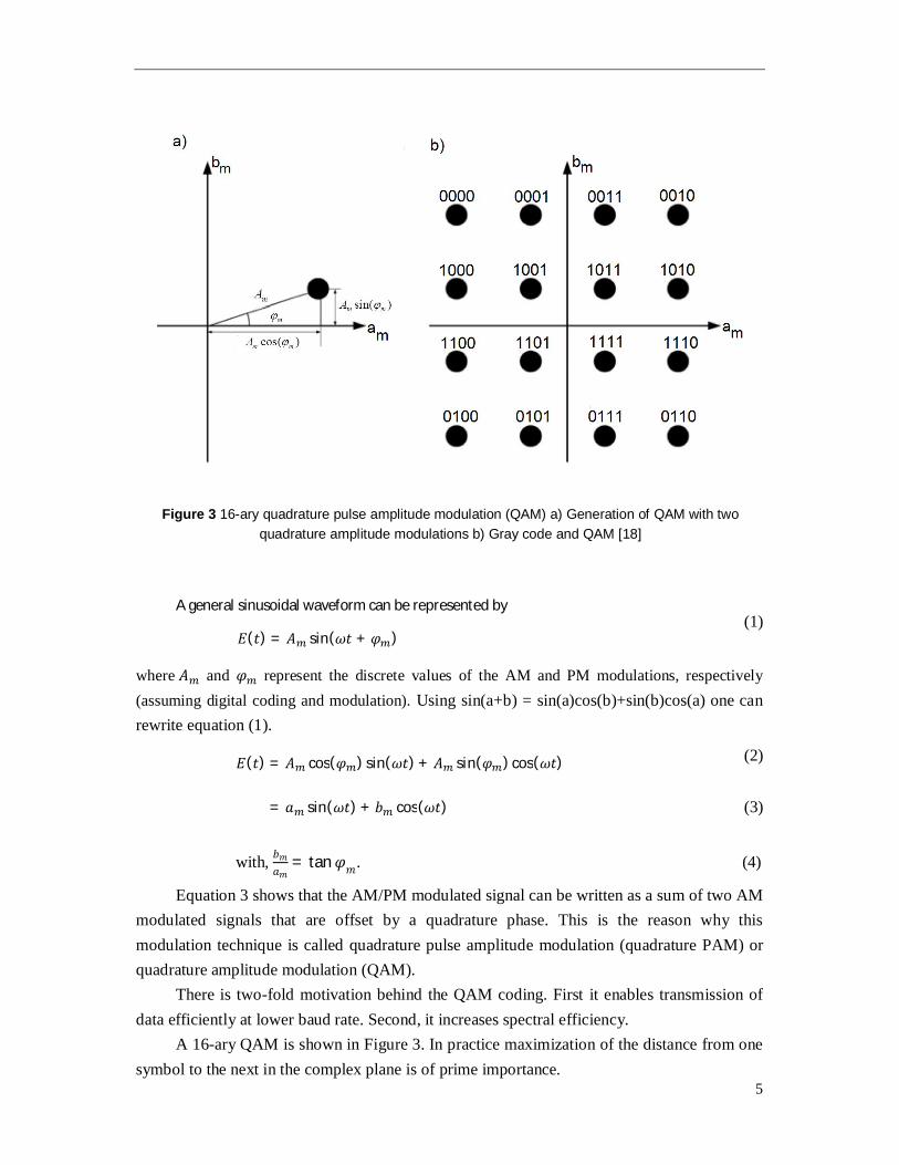
2.1.1 Quadrature Amplitude Modulation (QAM) A harmonic signal is represented by its amplitude and phase information, as shown in equation 1. Information can be modulated on the amplitude component, phase component, or both. The process of modulating information on the amplitude of the harmonic signal is known as Amplitude Modulation (AM) or Amplitude Shift Keying (ASK) in the digital domain. Similarly, the process of modulating information on the phase of the signal is known as Phase Modulation (PM) or Phase Shift Keying (PSK) in the digital domain. In order to increase the information transmitted on the single carrier, the obvious process would be utilize phase and amplitude information simultaneously. The mathematical representation of simultaneous coding is as follows:
5
A general sinusoidal waveform can be represented by
퐸(푡) = 퐴 sin(휔푡 +휑 ) (1)
where 퐴 and 휑 represent the discrete values of the AM and PM modulations, respectively (assuming digital coding and modulation). Using sin(a+b) = sin(a)cos(b)+sin(b)cos(a) one can rewrite equation (1).
퐸(푡) = 퐴 cos(휑 ) sin(휔푡) + 퐴 sin(휑 ) cos(휔푡) (2)
= 푎 sin(휔푡) + 푏 cos(휔푡) (3)
with, 푏푚푎푚
= tan휑푚. (4)
Equation 3 shows that the AM/PM modulated signal can be written as a sum of two AM modulated signals that are offset by a quadrature phase. This is the reason why this modulation technique is called quadrature pulse amplitude modulation (quadrature PAM) or quadrature amplitude modulation (QAM).
There is two-fold motivation behind the QAM coding. First it enables transmission of data efficiently at lower baud rate. Second, it increases spectral efficiency.
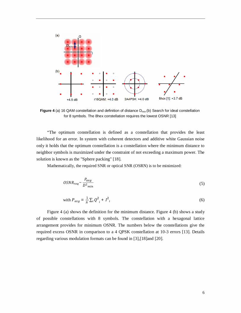
A 16-ary QAM is shown in Figure 3. In practice maximization of the distance from one symbol to the next in the complex plane is of prime importance.
Figure 3 16-ary quadrature pulse amplitude modulation (QAM) a) Generation of QAM with two quadrature amplitude modulations b) Gray code and QAM [18]
6
“The optimum constellation is defined as a constellation that provides the least
likelihood for an error. In system with coherent detectors and additive white Gaussian noise only it holds that the optimum constellation is a constellation where the minimum distance to neighbor symbols is maximized under the constraint of not exceeding a maximum power. The solution is known as the "Sphere packing" [18].
Mathematically, the required SNR or optical SNR (OSRN) is to be minimized:
푂푆푁푅 ~푃퐷
(5)
with 푃푎푣푔 = 1푁 ∑ 푄2
푖 + 퐼2푖푖 (6)
Figure 4 (a) shows the definition for the minimum distance. Figure 4 (b) shows a study of possible constellations with 8 symbols. The constellation with a hexagonal lattice arrangement provides for minimum OSNR. The numbers below the constellations give the required excess OSNR in comparison to a 4 QPSK constellation at 10-3 errors [13]. Details regarding various modulation formats can be found in [3],[18]and [20].
Figure 4 (a) 16 QAM constellation and definition of distance Dmin (b) Search for ideal constellation for 8 symbols. The 8hex constellation requires the lowest OSNR [13]
7
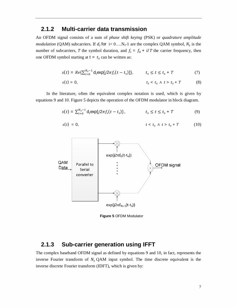
2.1.2 Multi-carrier data transmission An OFDM signal consists of a sum of phase shift keying (PSK) or quadrature amplitude modulation (QAM) subcarriers. If 푑 for i= 0….Ns-1 are the complex QAM symbol, 푁 is the number of subcarriers, 푇 the symbol duration, and 푓 = 푓 + 푖/푇 the carrier frequency, then one OFDM symbol starting at t = 푡 can be written as:
푠(푡) = 푅푒{∑ d exp[푗2휋푓 (푡 − 푡 )]}, 푡 ≤ 푡 ≤ 푡 + 푇 (7)
푠(푡) = 0, 푡 < 푡 ∧ 푡 > 푡 + 푇 (8)
In the literature, often the equivalent complex notation is used, which is given by equations 9 and 10. Figure 5 depicts the operation of the OFDM modulator in block diagram. 푠(푡) = ∑ d exp[푗2휋푓 (푡 − 푡 )] , 푡 ≤ 푡 ≤ 푡 + 푇 (9)
푠(푡) = 0, 푡 < 푡 ∧ 푡 > 푡 + 푇 (10)
2.1.3 Sub-carrier generation using IFFT The complex baseband OFDM signal as defined by equations 9 and 10, in fact, represents the inverse Fourier transform of 푁 QAM input symbol. The time discrete equivalent is the inverse discrete Fourier transform (IDFT), which is given by:
Figure 5 OFDM Modulator
8
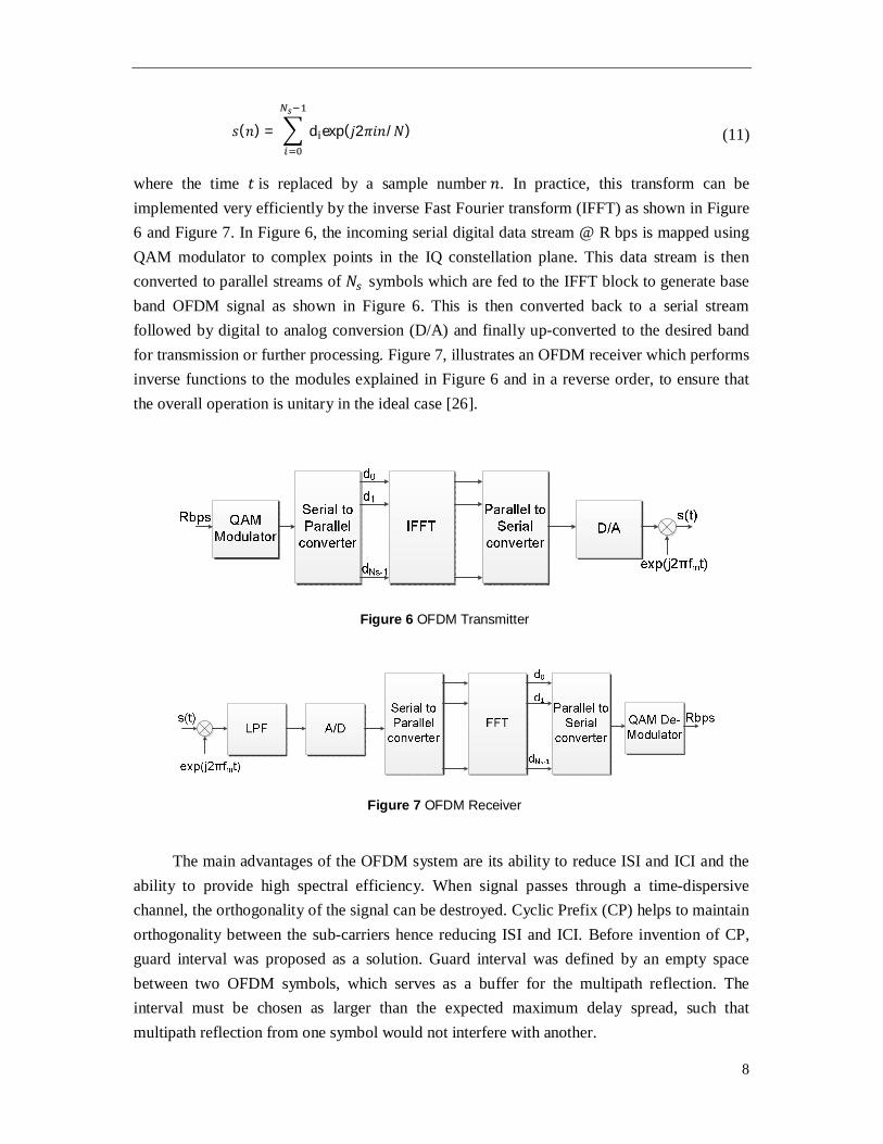
푠(푛) = d exp(푗2휋푖푛/푁) (11)
where the time 푡 is replaced by a sample number 푛. In practice, this transform can be implemented very efficiently by the inverse Fast Fourier transform (IFFT) as shown in Figure 6 and Figure 7. In Figure 6, the incoming serial digital data stream @ R bps is mapped using QAM modulator to complex points in the IQ constellation plane. This data stream is then converted to parallel streams of 푁 symbols which are fed to the IFFT block to generate base band OFDM signal as shown in Figure 6. This is then converted back to a serial stream followed by digital to analog conversion (D/A) and finally up-converted to the desired band for transmission or further processing. Figure 7, illustrates an OFDM receiver which performs inverse functions to the modules explained in Figure 6 and in a reverse order, to ensure that the overall operation is unitary in the ideal case [26].
The main advantages of the OFDM system are its ability to reduce ISI and ICI and the
ability to provide high spectral efficiency. When signal passes through a time-dispersive channel, the orthogonality of the signal can be destroyed. Cyclic Prefix (CP) helps to maintain orthogonality between the sub-carriers hence reducing ISI and ICI. Before invention of CP, guard interval was proposed as a solution. Guard interval was defined by an empty space between two OFDM symbols, which serves as a buffer for the multipath reflection. The interval must be chosen as larger than the expected maximum delay spread, such that multipath reflection from one symbol would not interfere with another.
Figure 7 OFDM Receiver
Figure 6 OFDM Transmitter
9
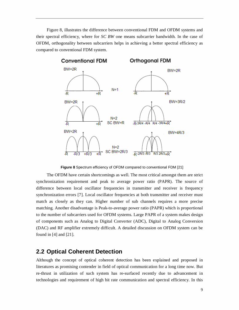
Figure 8, illustrates the difference between conventional FDM and OFDM systems and their spectral efficiency, where for SC BW one means subcarrier bandwidth. In the case of OFDM, orthogonality between subcarriers helps in achieving a better spectral efficiency as compared to conventional FDM system.
The OFDM have certain shortcomings as well. The most critical amongst them are strict synchronization requirement and peak to average power ratio (PAPR). The source of difference between local oscillator frequencies in transmitter and receiver is frequency synchronization errors [7]. Local oscillator frequencies at both transmitter and receiver must match as closely as they can. Higher number of sub channels requires a more precise matching. Another disadvantage is Peak-to-average power ratio (PAPR) which is proportional to the number of subcarriers used for OFDM systems. Large PAPR of a system makes design of components such as Analog to Digital Converter (ADC), Digital to Analog Conversion (DAC) and RF amplifier extremely difficult. A detailed discussion on OFDM system can be found in [4] and [21].
2.2 Optical Coherent Detection Although the concept of optical coherent detection has been explained and proposed in literatures as promising contender in field of optical communication for a long time now. But re-thrust in utilization of such system has re-surfaced recently due to advancement in technologies and requirement of high bit rate communication and spectral efficiency. In this
Figure 8 Spectrum efficiency of OFDM compared to conventional FDM [21]
10
section the basics of coherent detection are discussed. Various coherent detection schemes such as homodyne and heterodyne detection are covered. Various details of coherent detection systems can be found cumulatively in [1], [5], [6], [10], [12] and [19]
2.2.1 Optical Hybrid and Balanced Photo detection A coherent system design utilizes two important components. First, an optical hybrid used for mixing of the light beams. Second, balanced photo detectors used for optimal conversion of input optical fields into photocurrents.
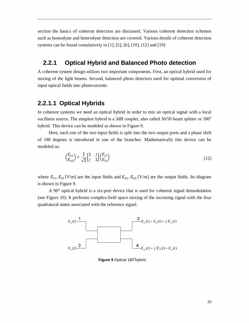
2.2.1.1 Optical Hybrids In coherent systems we need an optical hybrid in order to mix an optical signal with a local oscillator source. The simplest hybrid is a 3dB coupler, also called 50/50 beam splitter or 180o
hybrid. This device can be modeled as shown in Figure 9. Here, each one of the two input fields is split into the two output ports and a phase shift
of 180 degrees is introduced in one of the branches. Mathematically this device can be modeled as:
퐸퐸 =
1√2
1 푗푗 1
퐸퐸 (12)
where 퐸 , 퐸 [V/m] are the input fields and 퐸 , 퐸 [V/m] are the output fields. Its diagram is shown in Figure 9.
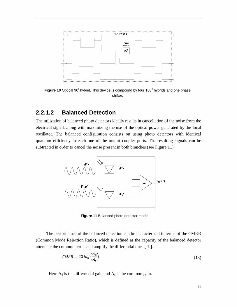
A 90° optical hybrid is a six-port device that is used for coherent signal demodulation (see Figure 10). It performs complex-field space mixing of the incoming signal with the four quadratural states associated with the reference signal.
1( )iE t
2 ( )iE t
1 1 2( ) ( ) ( )o i iE t E t j E t
2 1 2( ) ( ) ( )o i iE t j E t E t
Figure 9 Optical 180ohybrid.
11
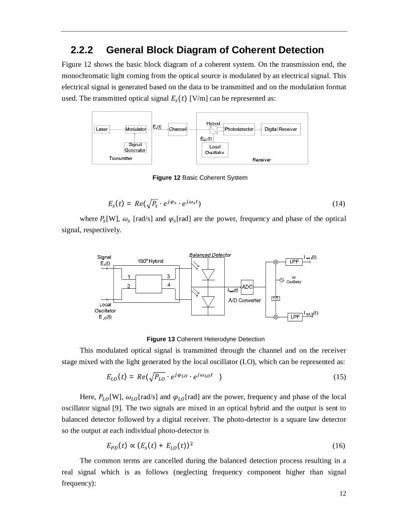
2.2.1.2 Balanced Detection The utilization of balanced photo detectors ideally results in cancellation of the noise from the electrical signal, along with maximizing the use of the optical power generated by the local oscillator. The balanced configuration consists on using photo detectors with identical quantum efficiency in each one of the output coupler ports. The resulting signals can be subtracted in order to cancel the noise present in both branches (see Figure 11).
The performance of the balanced detection can be characterized in terms of the CMRR
(Common Mode Rejection Ratio), which is defined as the capacity of the balanced detector attenuate the common terms and amplify the differential ones [ 1 ].
퐶푀푅푅 = 20 푙표푔퐴퐴
(13)
Here Ad is the differential gain and As is the common gain.
Figure 10 Optical 90o hybrid. This device is compound by four 180o hybrids and one phase shifter.
Figure 11 Balanced photo detector model.
12
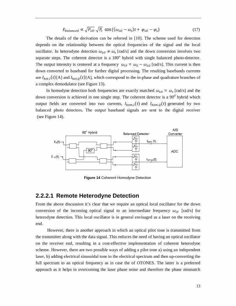
2.2.2 General Block Diagram of Coherent Detection Figure 12 shows the basic block diagram of a coherent system. On the transmission end, the monochromatic light coming from the optical source is modulated by an electrical signal. This electrical signal is generated based on the data to be transmitted and on the modulation format used. The transmitted optical signal 퐸 (푡) [V/m] can be represented as:
퐸 (푡) = 푅푒( 푃 ∙ 푒 ∙ 푒 ) (14)
where 푃 [W], 휔 [rad/s] and 휑 [rad] are the power, frequency and phase of the optical signal, respectively.
This modulated optical signal is transmitted through the channel and on the receiver stage mixed with the light generated by the local oscillator (LO), which can be represented as:
퐸 (푡) = 푅푒( 푃 ∙ 푒 ∙ 푒 ) (15)
Here, 푃 [W], 휔 [rad/s] and 휑 [rad] are the power, frequency and phase of the local oscillator signal [9]. The two signals are mixed in an optical hybrid and the output is sent to balanced detector followed by a digital receiver. The photo-detector is a square law detector so the output at each individual photo-detector is
퐸 (푡) ∝ (퐸 (푡) + 퐸 (푡)) (16)
The common terms are cancelled during the balanced detection process resulting in a real signal which is as follows (neglecting frequency component higher than signal frequency):
Figure 12 Basic Coherent System
Figure 13 Coherent Heterodyne Detection
13
퐸 ∝ 푃 . 푃 cos ((휔 −휔 )푡 + 휑 − 휑 ) (17)
The details of the derivation can be referred in [10]. The scheme used for detection depends on the relationship between the optical frequencies of the signal and the local oscillator. In heterodyne detection 휔 ≠ 휔 [rad/s] and the down conversion involves two separate steps. The coherent detector is a 180o hybrid with single balanced photo-detector. The output intensity is centered at a frequency 휔 = 휔 −휔 [rad/s]. This current is then down converted to baseband for further digital processing. The resulting basebands currents are 퐼 , (푡)[A] and 퐼 , (푡)[A], which correspond to the in-phase and quadrature branches of a complex demodulator (see Figure 13).
In homodyne detection both frequencies are exactly matched 휔 = 휔 [rad/s] and the down conversion is achieved in one single step. The coherent detector is a 900 hybrid which output fields are converted into two currents, 퐼 , (푡) and 퐼 , (푡) generated by two balanced photo detectors. The output baseband signals are sent to the digital receiver (see Figure 14).
2.2.2.1 Remote Heterodyne Detection From the above discussion it’s clear that we require an optical local oscillator for the down conversion of the incoming optical signal to an intermediate frequency 휔 [rad/s] for heterodyne detection. This local oscillator is in general envisaged as a laser on the receiving end.
However, there is another approach in which an optical pilot tone is transmitted from the transmitter along with the data signal. This reduces the need of having an optical oscillator on the receiver end, resulting in a cost-effective implementation of coherent heterodyne scheme. However, there are two possible ways of adding a pilot tone a) using an independent laser, b) adding electrical sinusoidal tone to the electrical spectrum and then up-converting the full spectrum to an optical frequency as in case the of OTONES. The latter is a preferred approach as it helps in overcoming the laser phase noise and therefore the phase mismatch
Figure 14 Coherent Homodyne Detection
14
between the two lasers within the system and it also prevents optical beat interference that might occur to frequency offset.
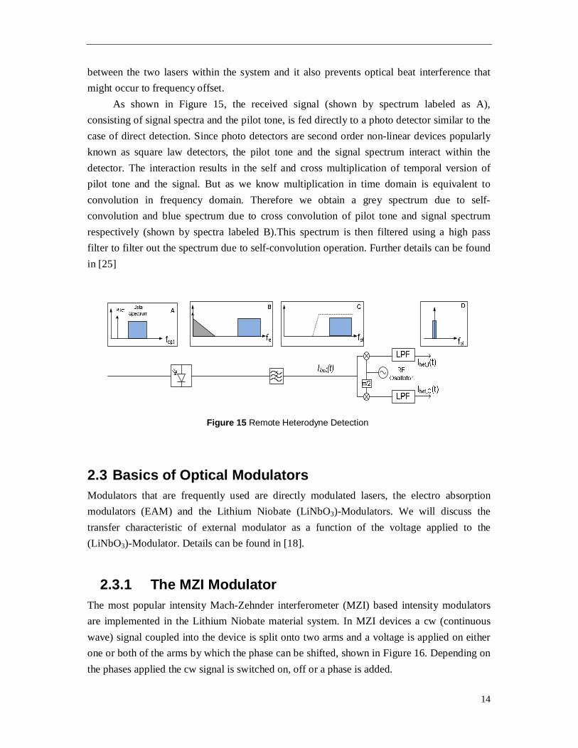
As shown in Figure 15, the received signal (shown by spectrum labeled as A), consisting of signal spectra and the pilot tone, is fed directly to a photo detector similar to the case of direct detection. Since photo detectors are second order non-linear devices popularly known as square law detectors, the pilot tone and the signal spectrum interact within the detector. The interaction results in the self and cross multiplication of temporal version of pilot tone and the signal. But as we know multiplication in time domain is equivalent to convolution in frequency domain. Therefore we obtain a grey spectrum due to self-convolution and blue spectrum due to cross convolution of pilot tone and signal spectrum respectively (shown by spectra labeled B).This spectrum is then filtered using a high pass filter to filter out the spectrum due to self-convolution operation. Further details can be found in [25]
2.3 Basics of Optical Modulators Modulators that are frequently used are directly modulated lasers, the electro absorption modulators (EAM) and the Lithium Niobate (LiNbO3)-Modulators. We will discuss the transfer characteristic of external modulator as a function of the voltage applied to the (LiNbO3)-Modulator. Details can be found in [18].
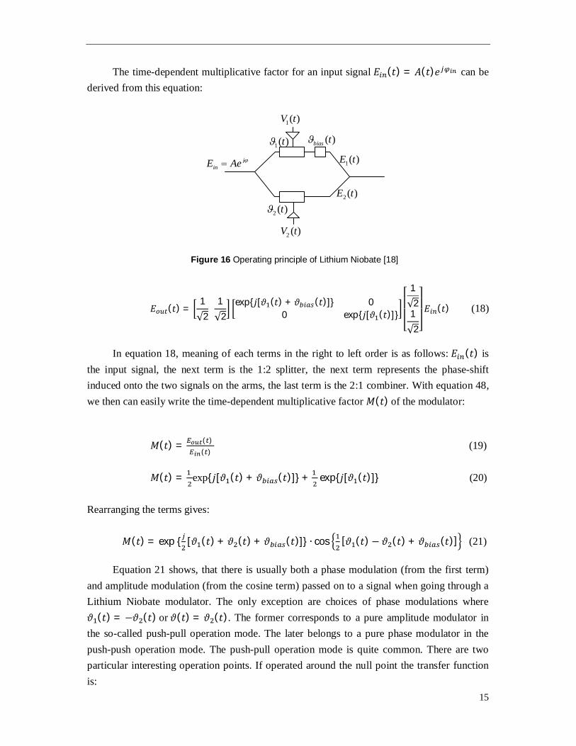
2.3.1 The MZI Modulator The most popular intensity Mach-Zehnder interferometer (MZI) based intensity modulators are implemented in the Lithium Niobate material system. In MZI devices a cw (continuous wave) signal coupled into the device is split onto two arms and a voltage is applied on either one or both of the arms by which the phase can be shifted, shown in Figure 16. Depending on the phases applied the cw signal is switched on, off or a phase is added.
Figure 15 Remote Heterodyne Detection
15
The time-dependent multiplicative factor for an input signal 퐸 (푡) = 퐴(푡)푒 can be derived from this equation:
퐸 (푡) =1√2
1√2
exp{푗[휗 (푡) + 휗 (푡)]} 00 exp{푗[휗 (푡)]}
⎣⎢⎢⎡
1√21√2⎦⎥⎥⎤퐸 (푡) (18)
In equation 18, meaning of each terms in the right to left order is as follows: 퐸 (푡) is the input signal, the next term is the 1:2 splitter, the next term represents the phase-shift induced onto the two signals on the arms, the last term is the 2:1 combiner. With equation 48, we then can easily write the time-dependent multiplicative factor 푀(푡) of the modulator:
푀(푡) = ( ) ( )
(19)
푀(푡) = exp{푗[휗 (푡) + 휗 (푡)]} + exp{푗[휗 (푡)]} (20)
Rearranging the terms gives:
푀(푡) = exp { [휗 (푡) + 휗 (푡) + 휗 (푡)]} ∙ cos [휗 (푡) − 휗 (푡) + 휗 (푡)] (21)
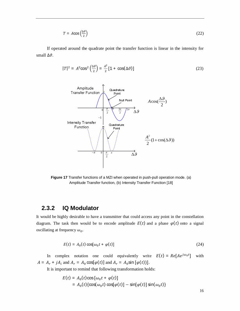
Equation 21 shows, that there is usually both a phase modulation (from the first term) and amplitude modulation (from the cosine term) passed on to a signal when going through a Lithium Niobate modulator. The only exception are choices of phase modulations where 휗 (푡) = −휗 (푡) or 휗(푡) = 휗 (푡). The former corresponds to a pure amplitude modulator in the so-called push-pull operation mode. The later belongs to a pure phase modulator in the push-push operation mode. The push-pull operation mode is quite common. There are two particular interesting operation points. If operated around the null point the transfer function is:
jinE Ae
1( )V t
2 ( )V t
1( )t
2 ( )t
( )bias t
1( )E t
2 ( )E t
Figure 16 Operating principle of Lithium Niobate [18]
16
푇 = 퐴cos ∆ (22)
If operated around the quadrate point the transfer function is linear in the intensity for small ∆휗.
|푇| = 퐴 cos ∆ = [1 + cos(∆휗)] (23)
2.3.2 IQ Modulator It would be highly desirable to have a transmitter that could access any point in the constellation diagram. The task then would be to encode amplitude 퐸(푡) and a phase 휑(푡) onto a signal oscillating at frequency 휔 .
퐸(푡) = 퐴 (푡) cos[휔 푡 + 휑(푡)] (24)
In complex notation one could equivalently write 퐸(푡) = 푅푒[퐴푒 ] with 퐴 = 퐴 + 푗퐴 and 퐴 = 퐴 cos[휑(푡)] and 퐴 = 퐴 sin [휑(푡))].
It is important to remind that following transformation holds:
퐸(푡) = 퐴 (푡)cos [휔 푡 + 휑(푡)] = 퐴 (푡){cos(휔 푡) cos[휑(푡)]− sin[휑(푡)] sin(휔 푡)}
2
2
0 32 2
1
0
cos( )2
A
2
(1 cos( ))2A
1
Figure 17 Transfer functions of a MZI when operated in push-pull operation mode. (a) Amplitude Transfer function, (b) Intensity Transfer Function [18]
17
= 퐴 cos(휔 푡) − 퐴 sin(휔 푡) = 푅푒{[퐴 + 푗퐴 ][cos (휔 푡) + 푗sin (휔 푡)]} = 푅푒(퐴푒 ) (25)
2.3.2.1 MZI Modulator Solution With the MZI modulator depicted in Figure 16 and described by equation 21 one indeed can access any point in the complex constellation diagram. The point in equation 22 for instance can be accessed by selecting
휗 (푡) = 휑(푡) + arccos[퐴 (푡)] (26)
휗 (푡) =
휑(푡)2 − arcos[퐴 (푡)]
(27)
This solution could work well, yet it requires sophisticated control over the electrical signals.
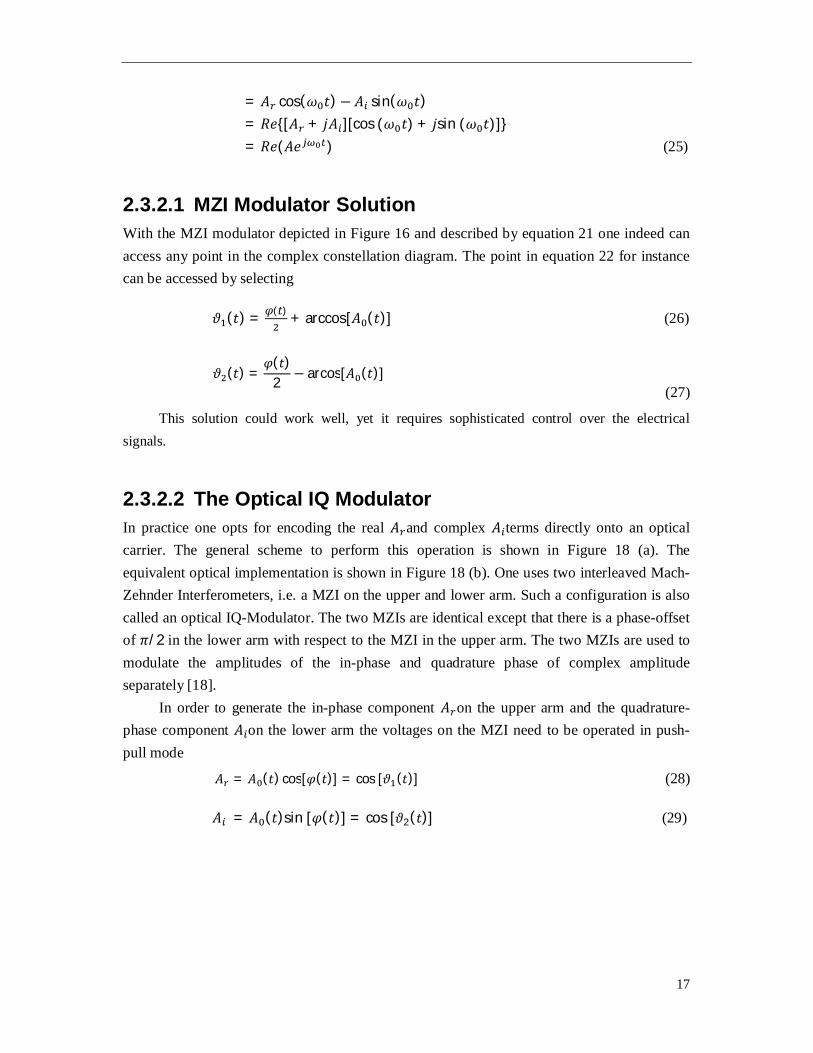
2.3.2.2 The Optical IQ Modulator In practice one opts for encoding the real 퐴 and complex 퐴 terms directly onto an optical carrier. The general scheme to perform this operation is shown in Figure 18 (a). The equivalent optical implementation is shown in Figure 18 (b). One uses two interleaved Mach- Zehnder Interferometers, i.e. a MZI on the upper and lower arm. Such a configuration is also called an optical IQ-Modulator. The two MZIs are identical except that there is a phase-offset of 휋/2 in the lower arm with respect to the MZI in the upper arm. The two MZIs are used to modulate the amplitudes of the in-phase and quadrature phase of complex amplitude separately [18].
In order to generate the in-phase component 퐴 on the upper arm and the quadrature-phase component 퐴 on the lower arm the voltages on the MZI need to be operated in push-pull mode
퐴 = 퐴 (푡) cos[휑(푡)] = cos [휗 (푡)] (28)
퐴 = 퐴 (푡)sin [휑(푡)] = cos [휗2(푡)] (29)
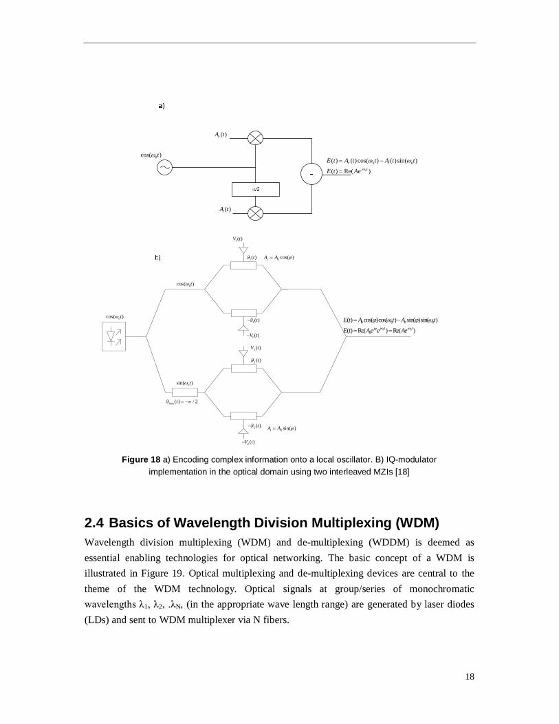
18
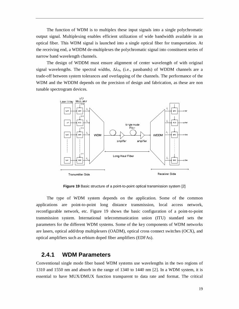
2.4 Basics of Wavelength Division Multiplexing (WDM) Wavelength division multiplexing (WDM) and de-multiplexing (WDDM) is deemed as essential enabling technologies for optical networking. The basic concept of a WDM is illustrated in Figure 19. Optical multiplexing and de-multiplexing devices are central to the theme of the WDM technology. Optical signals at group/series of monochromatic wavelengths λ1, λ2, .λN, (in the appropriate wave length range) are generated by laser diodes (LDs) and sent to WDM multiplexer via N fibers.
( )rA t
( )iA t
0cos( )t
0
0 0( ) ( )cos( ) ( ) sin( )
( ) Re( )r i
j t
E t A t t A t t
E t Ae
1( )V t
1( )t
1( )V t
2 ( )V t
2 ( )V t
1( )t
2 ( )t
2 ( )t
0cos( )t
0cos( )t
0sin( )t
( ) / 2bias t
0 cos( )rA A
0 sin( )iA A
0 0
0 0 0 0
0
( ) cos( )cos( ) sin( )sin( )
( ) Re( ) Re( )j t j tj
E t A t A t
E t Ae e Ae
Figure 18 a) Encoding complex information onto a local oscillator. B) IQ-modulator
implementation in the optical domain using two interleaved MZIs [18]
19
The function of WDM is to multiplex these input signals into a single polychromatic output signal. Multiplexing enables efficient utilization of wide bandwidth available in an optical fiber. This WDM signal is launched into a single optical fiber for transportation. At the receiving end, a WDDM de-multiplexes the polychromatic signal into constituent series of narrow band wavelength channels.
The design of WDDM must ensure alignment of center wavelength of with original signal wavelengths. The spectral widths, ΔλN, (i.e., passbands) of WDDM channels are a trade-off between system tolerances and overlapping of the channels. The performance of the WDM and the WDDM depends on the precision of design and fabrication, as these are non tunable spectrogram devices.
The type of WDM system depends on the application. Some of the common applications are point-to-point long distance transmission, local access network, reconfigurable network, etc. Figure 19 shows the basic configuration of a point-to-point transmission system. International telecommunication union (ITU) standard sets the parameters for the different WDM systems. Some of the key components of WDM networks are lasers, optical add/drop multiplexers (OADM), optical cross connect switches (OCX), and optical amplifiers such as erbium doped fiber amplifiers (EDFAs).
2.4.1 WDM Parameters Conventional single mode fiber based WDM systems use wavelengths in the two regions of 1310 and 1550 nm and absorb in the range of 1340 to 1440 nm [2]. In a WDM system, it is essential to have MUX/DMUX function transparent to data rate and format. The critical
1
2
3
n
1
2
3
n
Figure 19 Basic structure of a point-to-point optical transmission system [2]
20
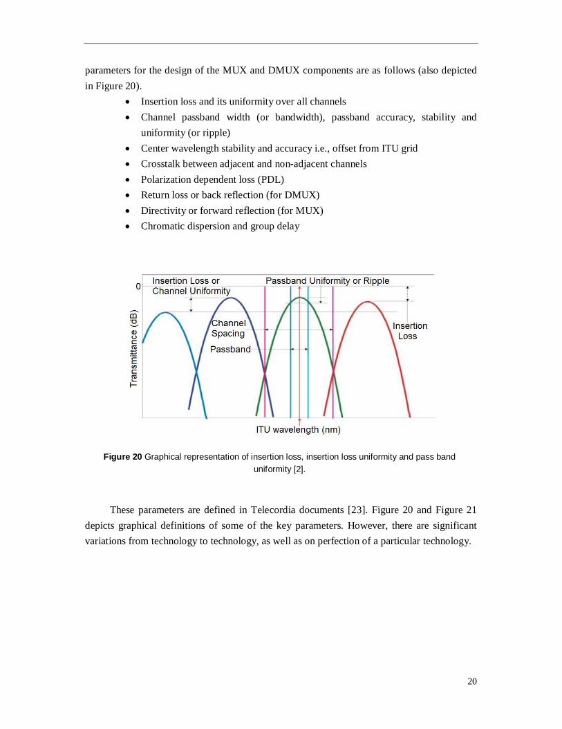
parameters for the design of the MUX and DMUX components are as follows (also depicted in Figure 20).
Insertion loss and its uniformity over all channels Channel passband width (or bandwidth), passband accuracy, stability and
uniformity (or ripple) Center wavelength stability and accuracy i.e., offset from ITU grid Crosstalk between adjacent and non-adjacent channels Polarization dependent loss (PDL) Return loss or back reflection (for DMUX) Directivity or forward reflection (for MUX) Chromatic dispersion and group delay
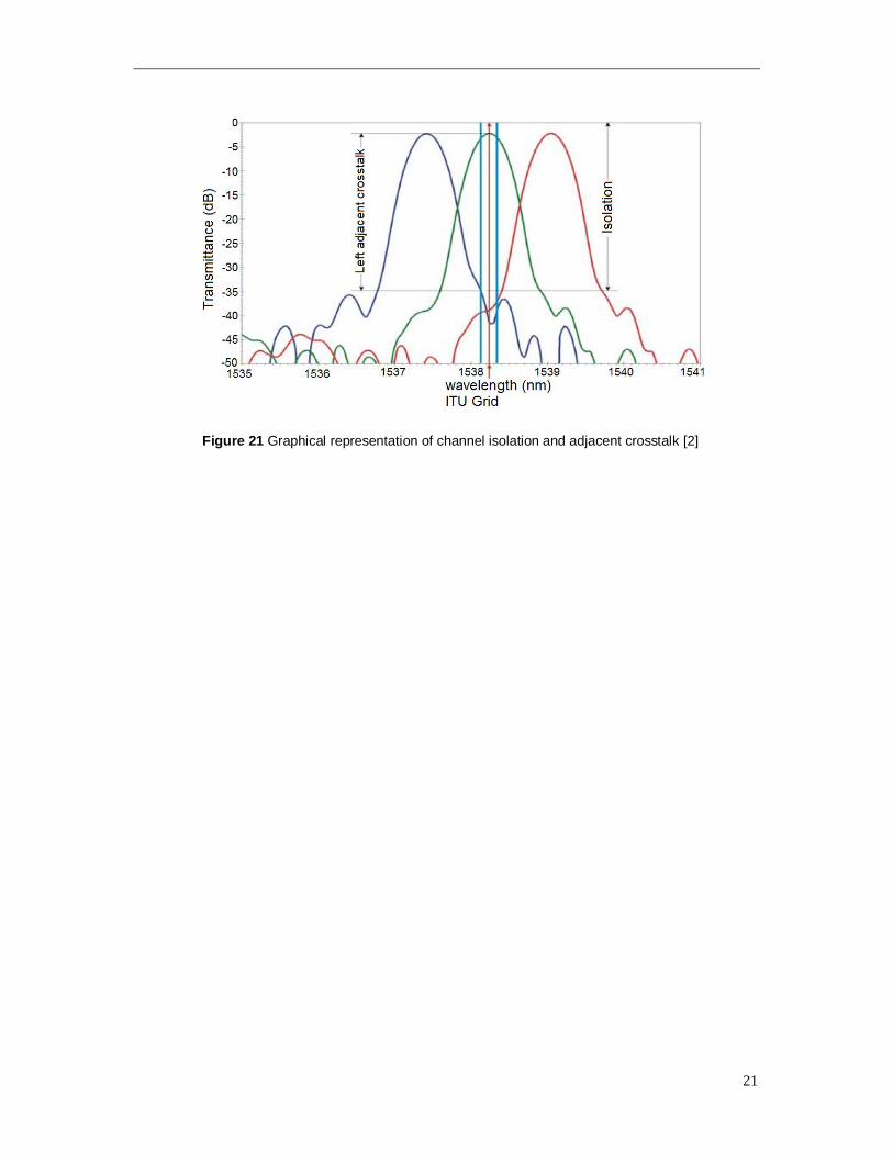
These parameters are defined in Telecordia documents [23]. Figure 20 and Figure 21
depicts graphical definitions of some of the key parameters. However, there are significant variations from technology to technology, as well as on perfection of a particular technology.
Figure 20 Graphical representation of insertion loss, insertion loss uniformity and pass band uniformity [2].
21
Figure 21 Graphical representation of channel isolation and adjacent crosstalk [2]
22
3 Single Side Band Modulation Techniques for Image Rejection
In this chapter, we discuss the problem and potential solutions for the rejection of image spectrum, also known as ghost spectrum, which originates during the up-conversion process for signal transmission through a desired channel. The first section of the chapter discusses the motivation for image rejection. Then, we formulate the requirements with respect to the OTONES projects. This is followed by an extensive review of various available methods to produce a Single Side Band (SSB). A Novel Bedrosian method for image rejection in OTONES is also proposed in this chapter. Finally, we present and discuss the simulation results for the selected methods which satisfy OTONES requirements and draw conclusions from the same.
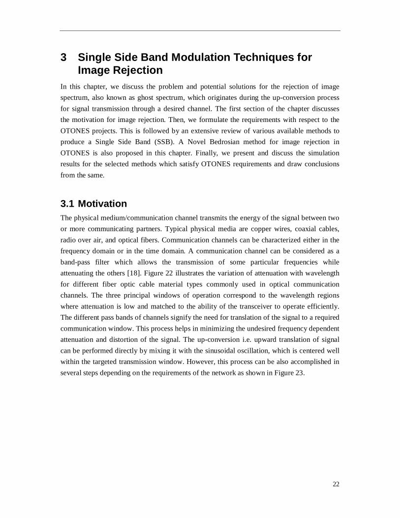
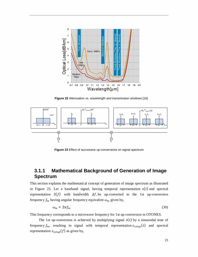
3.1 Motivation The physical medium/communication channel transmits the energy of the signal between two or more communicating partners. Typical physical media are copper wires, coaxial cables, radio over air, and optical fibers. Communication channels can be characterized either in the frequency domain or in the time domain. A communication channel can be considered as a band-pass filter which allows the transmission of some particular frequencies while attenuating the others [18]. Figure 22 illustrates the variation of attenuation with wavelength for different fiber optic cable material types commonly used in optical communication channels. The three principal windows of operation correspond to the wavelength regions where attenuation is low and matched to the ability of the transceiver to operate efficiently. The different pass bands of channels signify the need for translation of the signal to a required communication window. This process helps in minimizing the undesired frequency dependent attenuation and distortion of the signal. The up-conversion i.e. upward translation of signal can be performed directly by mixing it with the sinusoidal oscillation, which is centered well within the targeted transmission window. However, this process can be also accomplished in several steps depending on the requirements of the network as shown in Figure 23.
23
3.1.1 Mathematical Background of Generation of Image Spectrum
This section explains the mathematical concept of generation of image spectrum as illustrated in Figure 23. Let a baseband signal, having temporal representation 푠(푡) and spectral representation 푆(푓) with bandwidth 훥푓, be up-converted to the 1st up-conversion frequency 푓 having angular frequency equivalent 휔 given by,
휔 = 2휋푓 . (30)
This frequency corresponds to a microwave frequency for 1st up-conversion in OTONES. The 1st up-conversion is achieved by multiplying signal 푠(푡) by a sinusoidal tone of
frequency 푓 , resulting in signal with temporal representation 푠 (푡) and spectral representation 푠 (푓) as given by,
Figure 22 Attenuation vs. wavelength and transmission windows [16]
Figure 23 Effect of successive up-conversions on signal spectrum
24
푠 (푡) = 푠(푡) cos(휔 푡) (31)
2nd up-conversion is achieved by multiplying 푠 (푡) by sinusoidal tone of frequency 푓 , corresponding to optical frequency in OTONES, having angular frequency equivalent 휔 , given by,
휔 = 2휋푓 . (32)
This up-conversion results in a signal with temporal representation 푠 (푡) and spectral representation 푆 (푓) which is given by,
푠 (푡) = 푠 (푡) cos(휔 푡) (33)
Applying the trigonometric identity (34) to (33) we get (35),
cos(퐴). cos(퐵) =12 [cos(퐴 − 퐵) + cos(퐴 + 퐵)] (34)
푠 (푡) = 푠(푡) {cos[(휔 −휔 )푡] + cos[(휔 + 휔 )푡]} (35)
We can observe that single up-conversion produces double side band spectrum from the base-band signal. Performing a second up-conversion to a higher frequency, say 푓 , generates an image spectrum on the lower side due to different frequency generation. The two side bands after second up-conversion contain redundant information reducing the spectral efficiency by 3 dB. This ghost spectrum, per se lower side band in OTONES can act as an additional noise for the spectrum at that frequency band deteriorating the Signal to Noise Ratio (SNR) and thus the performance. It is this specific problem of ghost spectrum that we are dealing with in this chapter. This problem can be solved by applying an optimal SSB technique, as described in the subsequent sections.
3.2 Formulation of Requirements as per OTONES OTONES envisages 16-QAM OFDM modulation scheme to achieve high data rates. Since the signal is complex, both side bands of the base-band spectrum are required to retrieve the signal without any loss of data. As it was discussed previously in introduction section, the image spectrum is created after the optical up-conversion.
The requirements of OTONES for finding an optimal scheme to suppress the image spectrum are as following:
Preserving both side bands of the base band signal Inclusion of pilot tone in the downstream Achieve optimal spectral efficiency
25
Minimal circuital and computational complexity Cost effective and easy implementation Minimal spectral power loss during SSB generation Minimal phase distortion
3.3 Methods for Generation of SSB/ Image Rejection SSB generation is the process of elimination of all components of one of the side-bands from a modulated signal. A SSB signal comprises only of the upper or lower side band of a signal spectrum. As shown earlier, the successive up-conversions creates side-band having redundant information. Hence, no information is lost in the process of eliminating a sideband. In addition, since the final RF amplification is now concentrated in a single sideband, more information can be transmitted for the same power. We will describe various available methods for SSB generation in the following sub sections.
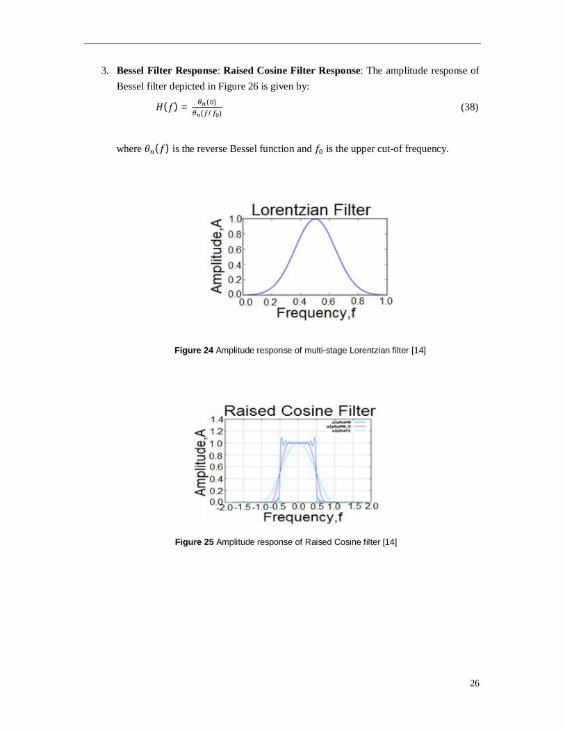
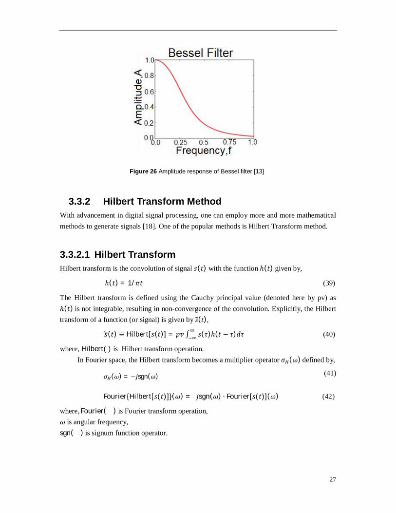
3.3.1 Filtering Methods Filtering is one method of producing a SSB signal by removing one of the side band, leaving only either the Upper Side Band (USB) or less commonly the Lower Side Band (LSB). Single Side Band Suppressed Carrier (SSB SC) is a most often case where the carrier is reduced or removed entirely (suppressed). Amplitude responses of some common filters are shown in Figure 24, Figure 25 and Figure 26.
1. Lorentzian Filter Response: The amplitude response of Lorentzian filter is given by:
퐿 (푓) = [ .( ) ( . )
] (36)
where 푓 is the central frequency and and Γ is a parameter specifying the band-width of filter and n is the order or number of cascaded stages of the multi-stage Lorentzian filter, amplitude response depicted in Figure 24.
2. Raised Cosine Filter Response: The amplitude response of Raised Cosine filter is given by:
퐻(푓) =푇,
0,1 + cos |푓| −
|푓| ≤
, < |푓| ≤표푡ℎ푒푟푤푖푠푒
(37)
where β is the roll off factor and T is the reciprocal of symbol rate. Amplitude response also depicted in Figure 25.
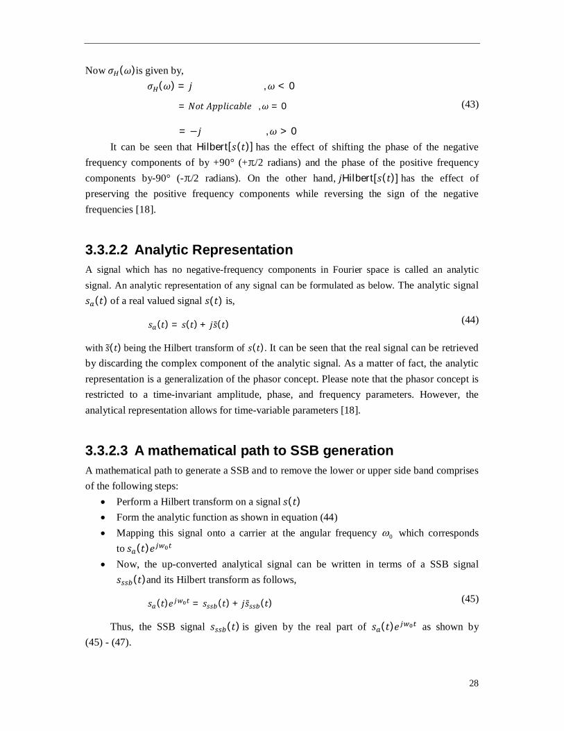
26
3. Bessel Filter Response: Raised Cosine Filter Response: The amplitude response of Bessel filter depicted in Figure 26 is given by:
퐻(푓) = ( )( / )
(38)
where 휃 (푓) is the reverse Bessel function and 푓 is the upper cut-of frequency.
Figure 25 Amplitude response of Raised Cosine filter [14]
Figure 24 Amplitude response of multi-stage Lorentzian filter [14]
27
3.3.2 Hilbert Transform Method With advancement in digital signal processing, one can employ more and more mathematical methods to generate signals [18]. One of the popular methods is Hilbert Transform method.
3.3.2.1 Hilbert Transform Hilbert transform is the convolution of signal 푠(푡) with the function ℎ(푡) given by,
ℎ(푡) = 1/휋푡 (39)
The Hilbert transform is defined using the Cauchy principal value (denoted here by pv) as ℎ(푡) is not integrable, resulting in non-convergence of the convolution. Explicitly, the Hilbert transform of a function (or signal) is given by 푠(푡),
푠(푡) ≡ Hilbert[푠(푡)] = 푝푣 ∫ 푠(휏)ℎ(푡 − 휏)푑휏 (40)
where, Hilbert( ) is Hilbert transform operation. In Fourier space, the Hilbert transform becomes a multiplier operator 휎 (휔) defined by,
휎 (휔) = −푗sgn(휔) (41)
Fourier{Hilbert[푠(푡)]}(휔) = 푗sgn(휔) ∙ Fourier[푠(푡)](휔) (42)
where, Fourier( ) is Fourier transform operation, 휔 is angular frequency, sgn( ) is signum function operator.
Figure 26 Amplitude response of Bessel filter [13]
28
Now 휎 (휔)is given by, 휎 (휔) = 푗 ,휔 < 0
= 푁표푡 퐴푝푝푙푖푐푎푏푙푒 ,휔 = 0 (43)
= −푗 ,휔 > 0 It can be seen that Hilbert[푠(푡)] has the effect of shifting the phase of the negative
frequency components of by +90° (+π/2 radians) and the phase of the positive frequency components by-90° (-π/2 radians). On the other hand, 푗Hilbert[푠(푡)] has the effect of preserving the positive frequency components while reversing the sign of the negative frequencies [18].
3.3.2.2 Analytic Representation A signal which has no negative-frequency components in Fourier space is called an analytic signal. An analytic representation of any signal can be formulated as below. The analytic signal 푠 (푡) of a real valued signal 푠(푡) is,
푠 (푡) = 푠(푡) + 푗푠̃(푡) (44)
with 푠(푡) being the Hilbert transform of 푠(푡). It can be seen that the real signal can be retrieved by discarding the complex component of the analytic signal. As a matter of fact, the analytic representation is a generalization of the phasor concept. Please note that the phasor concept is restricted to a time-invariant amplitude, phase, and frequency parameters. However, the analytical representation allows for time-variable parameters [18].
3.3.2.3 A mathematical path to SSB generation A mathematical path to generate a SSB and to remove the lower or upper side band comprises of the following steps:
Perform a Hilbert transform on a signal 푠(푡) Form the analytic function as shown in equation (44) Mapping this signal onto a carrier at the angular frequency 0 which corresponds
to 푠 (푡)푒 Now, the up-converted analytical signal can be written in terms of a SSB signal
푠 (푡)and its Hilbert transform as follows,
푠 (푡)푒 = 푠 (푡) + 푗푠̃ (푡) (45)
Thus, the SSB signal 푠 (푡) is given by the real part of 푠 (푡)푒 as shown by (45) - (47).
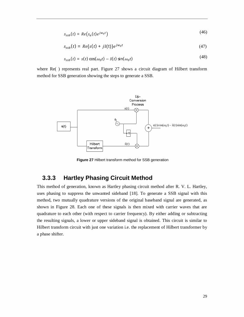
29
푠 (푡) = 푅푒 푠 (푡)푒 (46)
푠 (푡) = 푅푒{푠(푡) + 푗푠̃(t)}푒 (47)
푠 (푡) = 푠(푡) cos(휔 푡)− 푠̃(푡) sin(휔 푡) (48)
where Re( ) represents real part. Figure 27 shows a circuit diagram of Hilbert transform method for SSB generation showing the steps to generate a SSB.
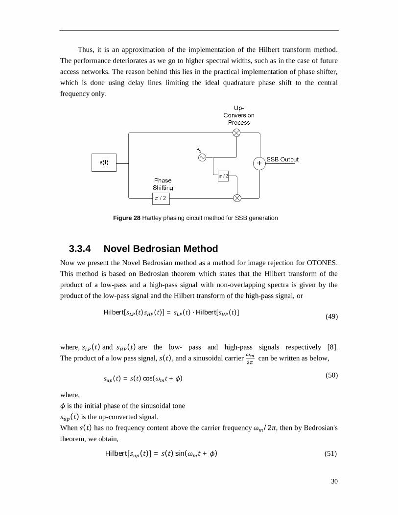
3.3.3 Hartley Phasing Circuit Method This method of generation, known as Hartley phasing circuit method after R. V. L. Hartley, uses phasing to suppress the unwanted sideband [18]. To generate a SSB signal with this method, two mutually quadrature versions of the original baseband signal are generated, as shown in Figure 28. Each one of these signals is then mixed with carrier waves that are quadrature to each other (with respect to carrier frequency). By either adding or subtracting the resulting signals, a lower or upper sideband signal is obtained. This circuit is similar to Hilbert transform circuit with just one variation i.e. the replacement of Hilbert transformer by a phase shifter.
( )s t
( )s t
0 0( )cos( ) ( )sin( )s t t s t t
Figure 27 Hilbert transform method for SSB generation
30
Thus, it is an approximation of the implementation of the Hilbert transform method. The performance deteriorates as we go to higher spectral widths, such as in the case of future access networks. The reason behind this lies in the practical implementation of phase shifter, which is done using delay lines limiting the ideal quadrature phase shift to the central frequency only.
3.3.4 Novel Bedrosian Method Now we present the Novel Bedrosian method as a method for image rejection for OTONES. This method is based on Bedrosian theorem which states that the Hilbert transform of the product of a low-pass and a high-pass signal with non-overlapping spectra is given by the product of the low-pass signal and the Hilbert transform of the high-pass signal, or
Hilbert[푠 (푡)푠 (푡)] = 푠 (푡) ∙ Hilbert[푠 (푡)]
(49)
where, 푠 (푡) and 푠 (푡) are the low- pass and high-pass signals respectively [8]. The product of a low pass signal, 푠(푡), and a sinusoidal carrier can be written as below,
푠 (푡) = 푠(푡) cos(휔 푡 +휙) (50)
where, 휙 is the initial phase of the sinusoidal tone 푠 (푡) is the up-converted signal. When 푠(푡) has no frequency content above the carrier frequency 휔 /2휋, then by Bedrosian's theorem, we obtain,
Hilbert[푠 (푡)] = 푠(푡) sin(휔 푡 + 휙) (51)
/ 2
/ 2
Figure 28 Hartley phasing circuit method for SSB generation
31
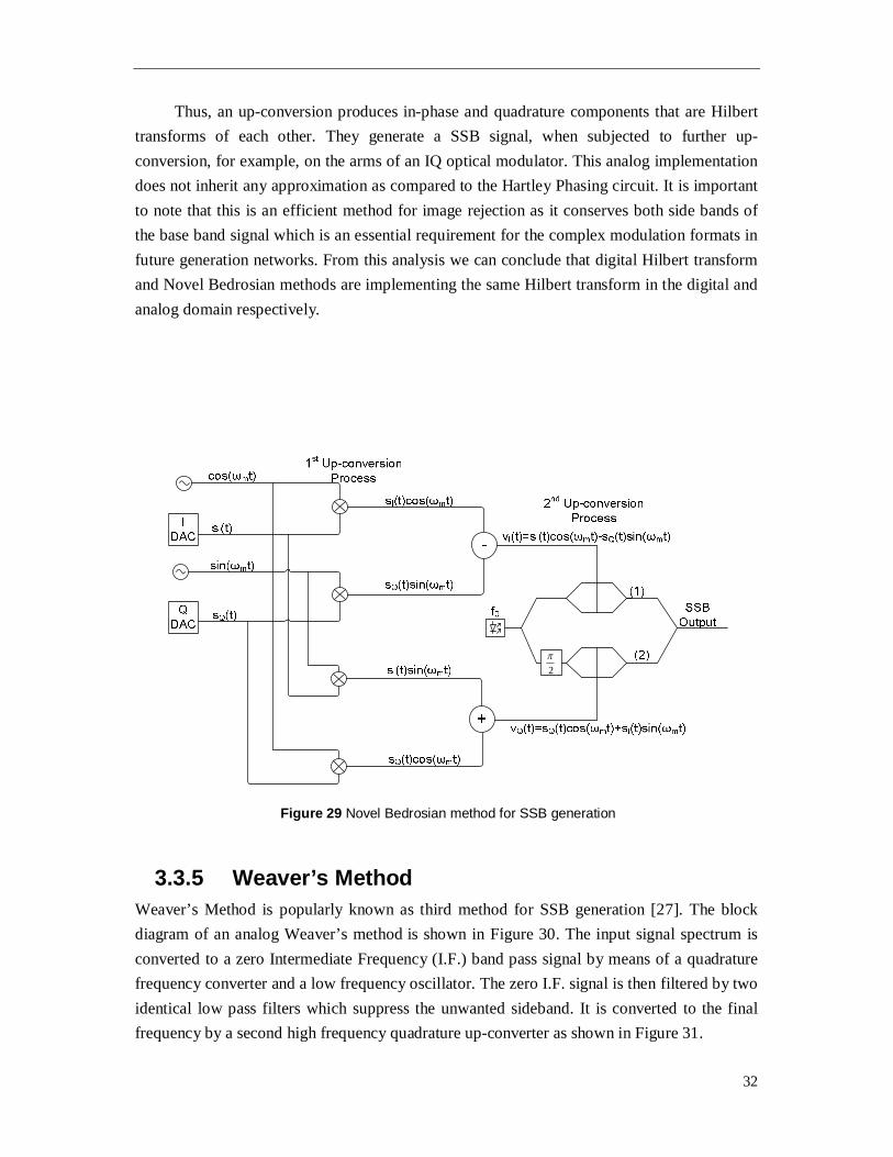
Thus, Hilbert transform pair can be generated by multiplying signal with quadrature tones. Figure 29 shows a Novel Bedrosian method circuit. The mathematical explanation of the circuit is provided below.
Let 푠(푡) a complex signal having in-phase component 푠 (푡) and quadrature component 푠 (푡) be given by,
푠(푡) = 푠 (푡) + 푗푠 (푡) (52)
Then up-conversion to frequency 푓 gives a signal represented by 푠 (푡) which is as shown below,
푠 (푡) = 푠(푡)푒 (53)
Applying equation (52) in (53) we get,
푠 (푡) = [푠 (푡) + 푗푠 (푡)]푒 (54)
Replacing 푒 by cos(2휋푓 푡) + 푗sin(2휋푓 푡) and expanding we get, 푠 (푡) = [푠 (푡) 푐표푠(2휋푓 푡)− 푠 (푡)푠푖푛(2휋푓 푡)] + 푗[푠 (푡)푠푖푛(2휋푓 푡) + 푠 (푡) 푐표푠(2휋푓 푡)] (55) Equation (53) can be rewritten as following,
푠 (푡) = 푣 (푡) + 푗푣 푡 (56)
where, 푣 (푡) and 푣 (푡) are in-phase and quadrature component of 푠 (푡) respectively, thus separating real and complex part we get,
푣 (푡) = 푠 (푡)cos (2π푓 푡) − 푠 (푡)sin (2π푓 푡) (57)
푣 (푡) = 푠 (푡)sin (2π푓 푡) + 푠 (푡)cos (2π푓 푡) (58)
Then applying the Hilbert transform on 푣 (푡), we get,
Hilbert[푣 (푡)] = Hilbert[푠 (푡)cos (2π푓 푡) − 푠 (푡)sin (2π푓 푡)] (59)
Applying linearity property of Hilbert transform to equation (58), we get,
Hilbert[푣 (푡)] = Hilbert[푠 (푡)cos (2π푓 푡)] − Hilbert[푠 (푡)sin (2휋푓 푡))] (60)
Applying Bedrosian theorem to equation (60), we get,
Hilbert[푣 (푡)] = 푠 (푡)Hilbert[푐표푠 (2π푓 푡)]− 푠 (t)Hilbert[sin (2π푓 푡)] (61) Thus,
Hilbert[푣 (푡)] = 푠 (푡)sin (2π푓 푡) + 푠 (t)cos (2π푓 푡) (62)
Hilbert[푣 (푡)] = 푣 (푡) (63)
32
Thus, an up-conversion produces in-phase and quadrature components that are Hilbert transforms of each other. They generate a SSB signal, when subjected to further up-conversion, for example, on the arms of an IQ optical modulator. This analog implementation does not inherit any approximation as compared to the Hartley Phasing circuit. It is important to note that this is an efficient method for image rejection as it conserves both side bands of the base band signal which is an essential requirement for the complex modulation formats in future generation networks. From this analysis we can conclude that digital Hilbert transform and Novel Bedrosian methods are implementing the same Hilbert transform in the digital and analog domain respectively.
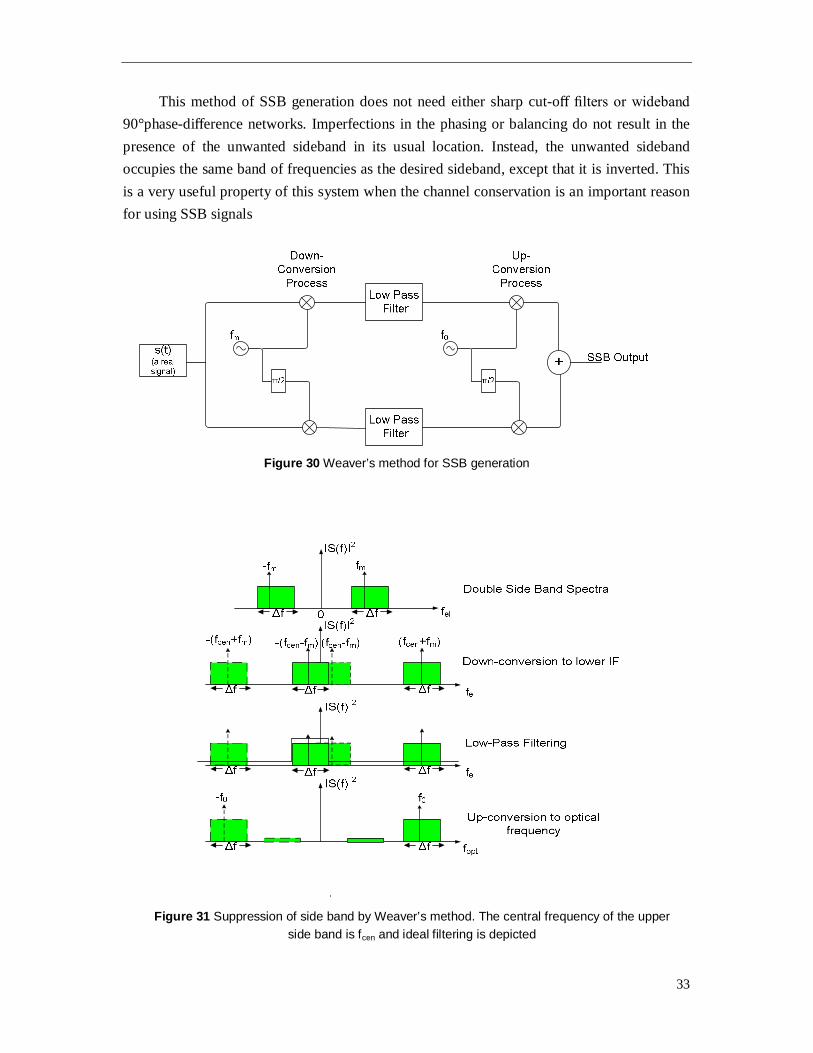
3.3.5 Weaver’s Method Weaver’s Method is popularly known as third method for SSB generation [27]. The block diagram of an analog Weaver’s method is shown in Figure 30. The input signal spectrum is converted to a zero Intermediate Frequency (I.F.) band pass signal by means of a quadrature frequency converter and a low frequency oscillator. The zero I.F. signal is then filtered by two identical low pass filters which suppress the unwanted sideband. It is converted to the final frequency by a second high frequency quadrature up-converter as shown in Figure 31.
2
Figure 29 Novel Bedrosian method for SSB generation
33
This method of SSB generation does not need either sharp cut-off filters or wideband 90°phase-difference networks. Imperfections in the phasing or balancing do not result in the presence of the unwanted sideband in its usual location. Instead, the unwanted sideband occupies the same band of frequencies as the desired sideband, except that it is inverted. This is a very useful property of this system when the channel conservation is an important reason for using SSB signals
Figure 31 Suppression of side band by Weaver’s method. The central frequency of the upper
side band is fcen and ideal filtering is depicted
Figure 30 Weaver’s method for SSB generation
34
3.4 Results and Discussion The analysis of the various methods was conducted for the requirement specifications given in OTONES. The signal bandwidth is denoted by 훥푓 and 1st up-conversion frequency is denoted by 푓 and 2nd up-conversion frequency is denoted by 푓 . As seen in the previous sections, if the SSB technique is applied directly to base band signals, then only the positive frequency spectrum i.e. the upper side band is preserved. This means that the Hilbert Transform method at base band frequencies cannot be applied, as it violates OTONES requirements stated in section 3.2. In order to preserve both side bands the signal is up-converted to an intermediate microwave frequency. Thus, we need to compare the methods with up-conversion as an essential and first common step.
Weaver’s method which comprises of down conversion to a lower I.F.as its integral part can be ruled out, as down-converting a signal is an extra step before the final up-conversion to optical frequencies. This would increase the hardware complexity without any significant advantage with respect to other methods.
Digital Hilbert transform is ideally identical to Novel Bedrosian method so there is no net gain in performance. Performing a Digital Hilbert transform is more hardware intensive because it requires high speed ADCs/DACs and FPGA to get the Hilbert transform at the up-converted frequency.
Hartley phasing circuit method is an approximation to the Hilbert transform generation. Since we have 16 QAM-OFDM modulation, which is phase sensitive along with a wide spectral band requirement, this method would generate phasing error. The phasing error would deteriorate the performance of the OFDM based topology due to unequal phase shift for frequencies in the spectrum.
SSB generation methods are analyzed for its performance limits based on the suppression depth performance. The suppression depth (S.D.) is defined as (see Figure 32):
Figure 33 shows the variation of suppression depth vs. side band separation (= 2 ∗ 푓 )
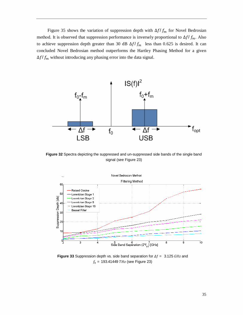
for various optical filtering methods discussed earlier. It can be observed that, Raised Cosine filter provides an upper bound to the filtering performance of the optical filters. While the Bessel filter provides a lower bound to the filtering performance. Performance of the Multi-stage Lorentzian filter increases with stages but is inversely proportional to 3 dB filtering bandwidth. For all filter types the suppression performance increases with the side band separation.
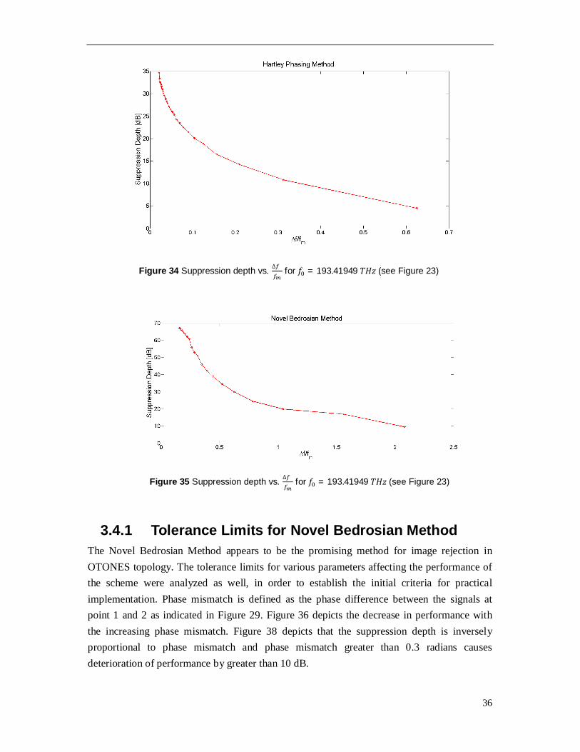
Figure 34 shows the variation of suppression depth with ∆푓/푓 for Hartley Phasing method. It is observed that suppression performance is inversely proportional to ∆푓/푓 . Also to achieve suppression depth greater than 30 dB ∆푓/푓 less than 0.03125 is desired.
Total power in undesired or suppressed side band after SSB. .Total power in desired side band after SSB
S D
35
Figure 35 shows the variation of suppression depth with ∆푓/푓 for Novel Bedrosian method. It is observed that suppression performance is inversely proportional to ∆푓/푓 . Also to achieve suppression depth greater than 30 dB ∆푓/푓 less than 0.625 is desired. It can concluded Novel Bedrosian method outperforms the Hartley Phasing Method for a given ∆푓/푓 without introducing any phasing error into the data signal.
Figure 32 Spectra depicting the suppressed and un-suppressed side bands of the single band signal (see Figure 23)
Figure 1 Suppression depth vs. ∆풇 풇풎
for 풇ퟎ = ퟏퟗퟑ.ퟒퟏퟗퟒퟗ 푻푯풛 (see Error! Reference source
Figure 33 Suppression depth vs. side band separation for 훥푓 = 3.125 퐺퐻푧 and
푓 = 193.41449 푇퐻푧 (see Figure 23)
36
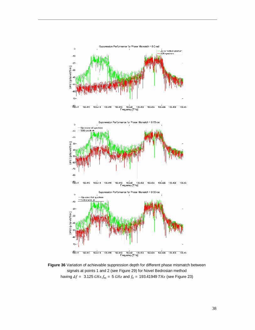
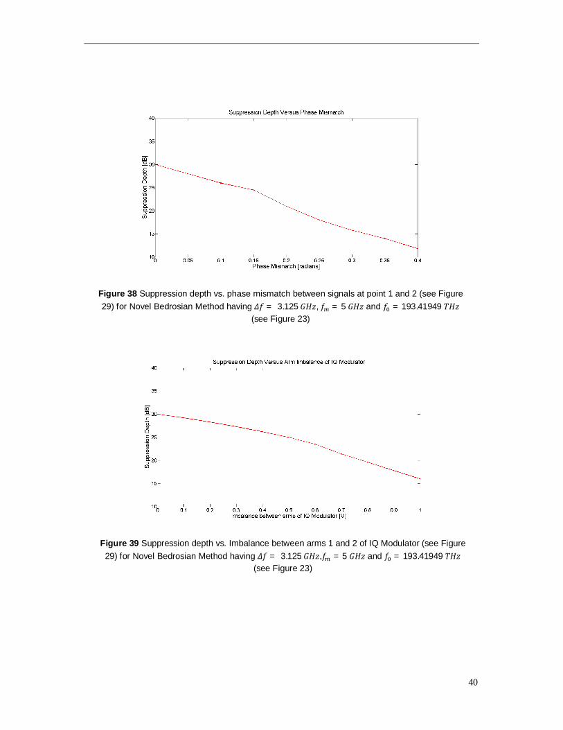
3.4.1 Tolerance Limits for Novel Bedrosian Method The Novel Bedrosian Method appears to be the promising method for image rejection in OTONES topology. The tolerance limits for various parameters affecting the performance of the scheme were analyzed as well, in order to establish the initial criteria for practical implementation. Phase mismatch is defined as the phase difference between the signals at point 1 and 2 as indicated in Figure 29. Figure 36 depicts the decrease in performance with the increasing phase mismatch. Figure 38 depicts that the suppression depth is inversely proportional to phase mismatch and phase mismatch greater than 0.3 radians causes deterioration of performance by greater than 10 dB.
Figure 34 Suppression depth vs. ∆ for 푓 = 193.41949 푇퐻푧 (see Figure 23)
Figure 35 Suppression depth vs. ∆ for 푓 = 193.41949 푇퐻푧 (see Figure 23)

37
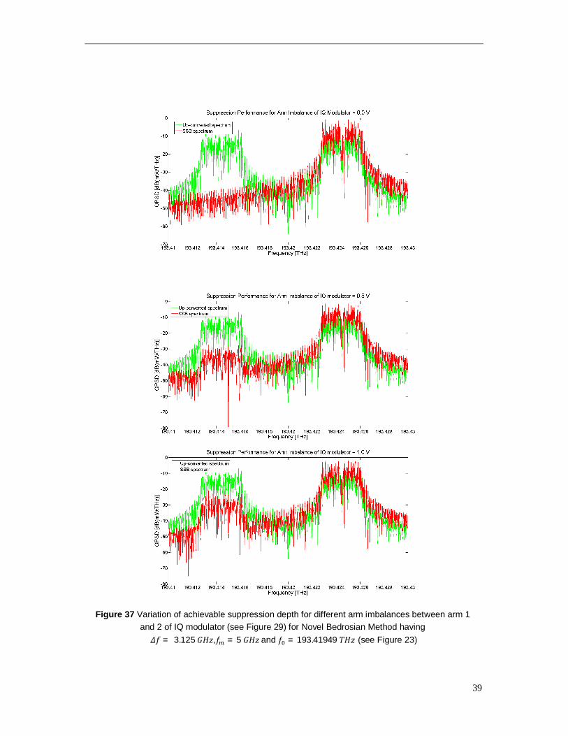
The imbalance between the two arms of IQ modulator is defined as the difference in the operating points of the arm 1 and 2 of the IQ modulator, indicated in Figure 29. Figure 37 depicts decrease in performance with increase in imbalance between the arms of the IQ modulator. Figure 39 shows that the suppression depth is inversely proportional to the imbalance between two arms of IQ modulator. Also for imbalance between two arms greater than 0.75 V causes a decrease of suppression depth by more than 10 dB.
38
Figure 36 Variation of achievable suppression depth for different phase mismatch between
signals at points 1 and 2 (see Figure 29) for Novel Bedrosian method having 훥푓 = 3.125 퐺퐻푧,푓 = 5 퐺퐻푧 and 푓 = 193.41949 푇퐻푧 (see Figure 23)
39
Figure 37 Variation of achievable suppression depth for different arm imbalances between arm 1
and 2 of IQ modulator (see Figure 29) for Novel Bedrosian Method having 훥푓 = 3.125 퐺퐻푧,푓 = 5 퐺퐻푧 and 푓 = 193.41949 푇퐻푧 (see Figure 23)
40
Figure 38 Suppression depth vs. phase mismatch between signals at point 1 and 2 (see Figure 29) for Novel Bedrosian Method having 훥푓 = 3.125 퐺퐻푧, 푓 = 5 퐺퐻푧 and 푓 = 193.41949 푇퐻푧
(see Figure 23)
Figure 39 Suppression depth vs. Imbalance between arms 1 and 2 of IQ Modulator (see Figure 29) for Novel Bedrosian Method having 훥푓 = 3.125 퐺퐻푧,푓 = 5 퐺퐻푧 and 푓 = 193.41949 푇퐻푧
(see Figure 23)
41
3.5 Conclusions This chapter provides a detailed discussion on the challenges and potential solutions of
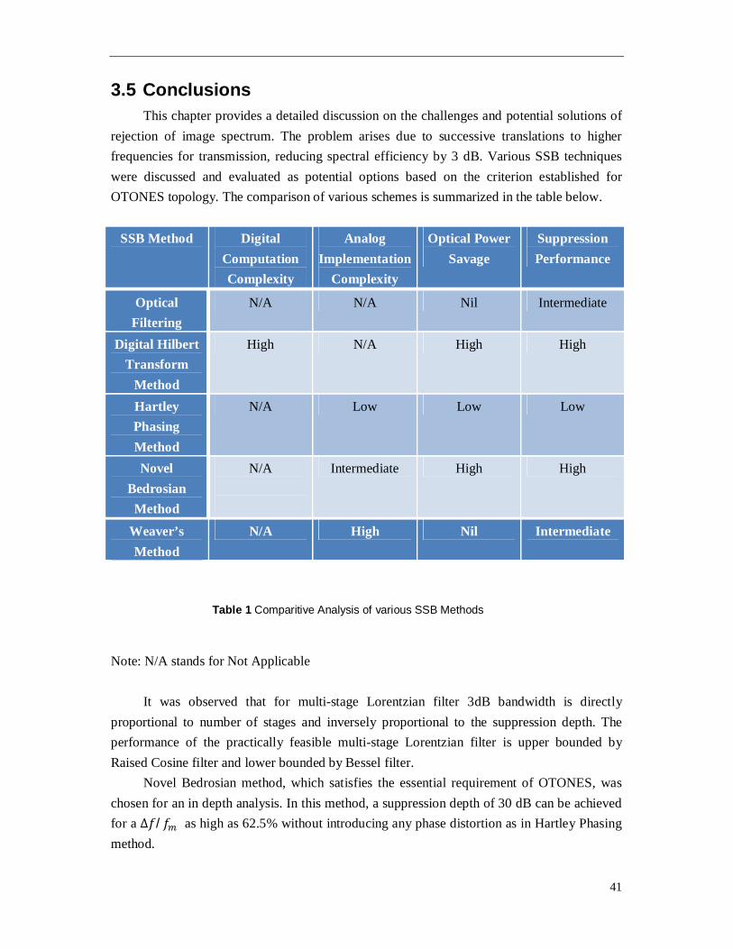
rejection of image spectrum. The problem arises due to successive translations to higher frequencies for transmission, reducing spectral efficiency by 3 dB. Various SSB techniques were discussed and evaluated as potential options based on the criterion established for OTONES topology. The comparison of various schemes is summarized in the table below.
SSB Method Digital
Computation Complexity
Analog Implementation
Complexity
Optical Power Savage
Suppression Performance
Optical Filtering
N/A N/A Nil Intermediate
Digital Hilbert Transform
Method
High N/A High High
Hartley Phasing Method
N/A Low Low Low
Novel Bedrosian Method
N/A
Intermediate High High
Weaver’s Method
N/A High Nil Intermediate
Note: N/A stands for Not Applicable It was observed that for multi-stage Lorentzian filter 3dB bandwidth is directly
proportional to number of stages and inversely proportional to the suppression depth. The performance of the practically feasible multi-stage Lorentzian filter is upper bounded by Raised Cosine filter and lower bounded by Bessel filter.
Novel Bedrosian method, which satisfies the essential requirement of OTONES, was chosen for an in depth analysis. In this method, a suppression depth of 30 dB can be achieved for a ∆푓/푓 as high as 62.5% without introducing any phase distortion as in Hartley Phasing method.
Table 1 Comparitive Analysis of various SSB Methods
42
The tolerance limits were established for the Novel Bedrosian method to provide theoretical bounds on the performance due to possible phase mismatch and imbalance between the two arms of the IQ Modulator. Deterioration in suppression performance of greater than 10 dB is observed for a phase mismatch of greater than 0.3 radians or an imbalance between the arms of the IQ modulators of greater than 0.75 V.
Therefore, Novel Bedrosian method with a suppression depth of approximately 30 dB is a considerable option for image rejection for the upstream path. It would result in saving 3 dB of power at Optical Network Unit (ONU). The downstream path involves the usage of pilot tone. Use of optical filtering turns out to be a better option in terms of suppression depth and circuit complexity.
43
4 Circuital Modeling of the OTONES Topology This chapter deals with the modeling aspects of various components in the OTONES network topology. The goal is to emulate realistic behavior of the network and its components to assist in visualization and verification of the network operation. An overview of the topology and its spectral design was discussed in the introduction chapter, wherein bi-directional concurrent behavior of the network having colorless ONU is underlined. Since the upstream data is modulated on the incoming downstream signal see Figure 2 therefore imparities and non-ideal behavior of the various components have a coupled effect on the overall network performance.
The modeling and simulation of topology was carried out on RSOFT’s OptSim which is a well-known simulation platform for optical networks. In traditional optical communication, involving On/Off Keying modulation, in general, the noise and other impairments in the electrical domain are suppressed in the optical domain. Thus using the simplistic models for the electrical drive circuits suffices simulation requirements for all practical purposes. In this thesis, the utilization of complex modulation format based coherent OFDM system is considered. Thus, effects of imparities in electrical domain components on overall system performance are interesting to analyze a pragmatic scenario. Since the OptSim provides for extremely simple model for the electrical domain components. The challenge was to emulate realistic models in the electrical domain as well in OptSim without inordinate effect on the simulation time and processing resources.
The simulations were carried out in the Sample mode Variable Bandwidth Simulation (VBS-SM) with full model to include all fiber effect, both linear and non-linear. This was most complete and powerful simulation strategy for our case. Various simulation parameters for executing the simulation is an efficient manner were set. Details of the parameters and other Optsim related information can be referred in sample mode simulation [22].
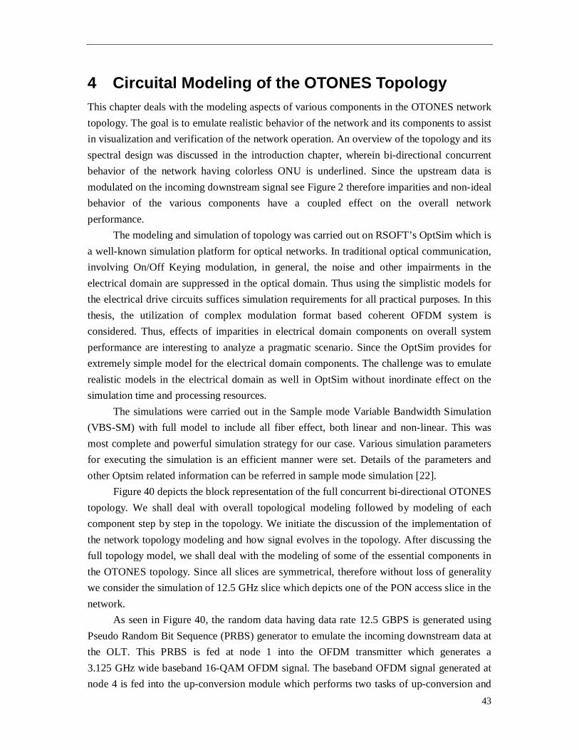
Figure 40 depicts the block representation of the full concurrent bi-directional OTONES topology. We shall deal with overall topological modeling followed by modeling of each component step by step in the topology. We initiate the discussion of the implementation of the network topology modeling and how signal evolves in the topology. After discussing the full topology model, we shall deal with the modeling of some of the essential components in the OTONES topology. Since all slices are symmetrical, therefore without loss of generality we consider the simulation of 12.5 GHz slice which depicts one of the PON access slice in the network.
As seen in Figure 40, the random data having data rate 12.5 GBPS is generated using Pseudo Random Bit Sequence (PRBS) generator to emulate the incoming downstream data at the OLT. This PRBS is fed at node 1 into the OFDM transmitter which generates a 3.125 GHz wide baseband 16-QAM OFDM signal. The baseband OFDM signal generated at node 4 is fed into the up-conversion module which performs two tasks of up-conversion and
44
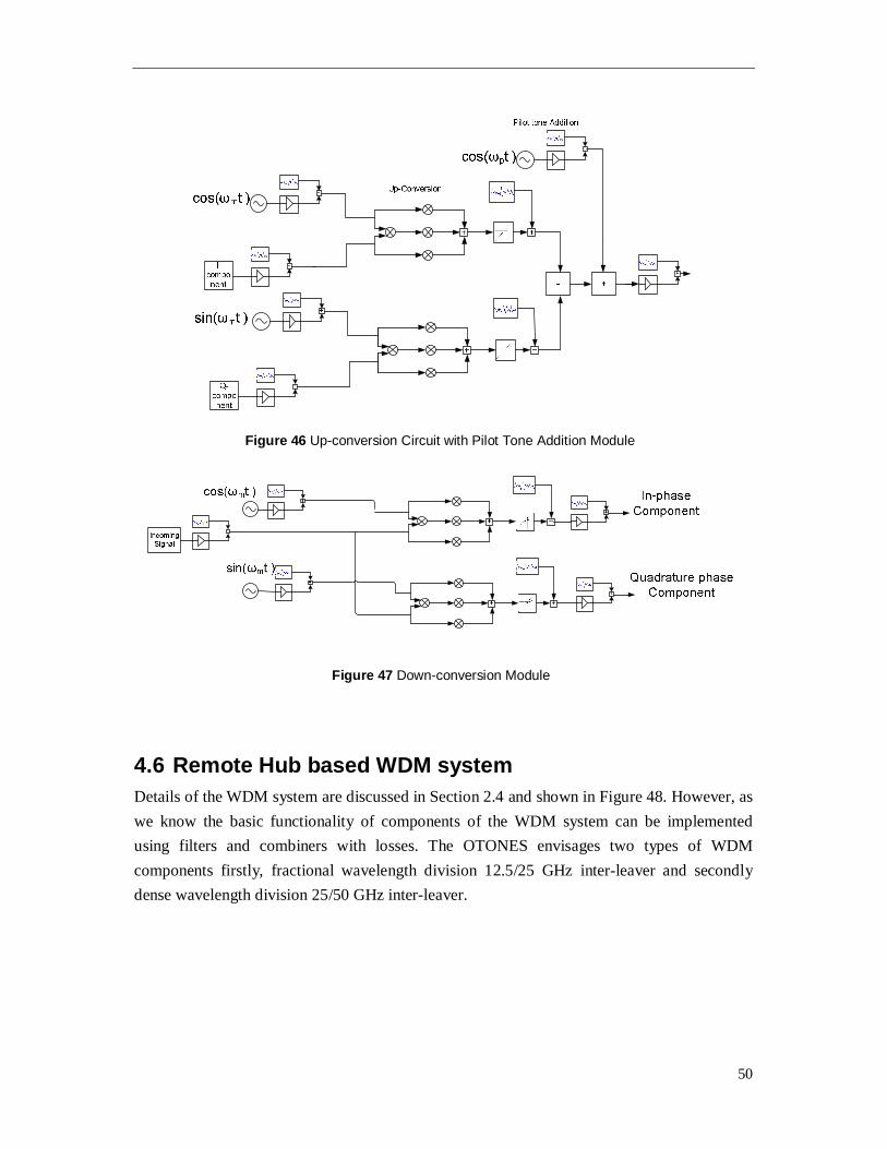
addition of pilot tone. Since we adhere to PUDG scheme therefore, the pilot is at the starting point of the PUDG spectral slot which is 12.5 GHz wide and each sub-band within PUDG is ∆푓 = 3.125 GHz wide. Therefore, the separation of the pilot tone to the mid of the downstream band is constant and is equal to 2.5 ∗ ∆푓. Thus, the up-conversion frequency on absolute frequency scale is pilot tone frequency 푓 + 2.5 ∗ ∆푓. The value of pilot frequency 푓 needs to be optimized for the topology. The up-converted signal at node 5 is modulated on the MZM dual arm modulator. The MZM modulator is operated at the null point to achieve suppression of the DC carrier tone. Since, the optical spectrum has a double side band spectra for reasons discussed in Chapter 3, the signal is passed through a band pass filter followed by amplification which results in a single side band spectra at node 6.
This signal is fed into the fiber attributing almost 6 dB loss in signal power along with inclusion of other imparities such as dispersion and more. The signal is fed into the remote hub module which performs the functions as discussed in Section 4.6. The signal output signal at node 13 is fed into the passive distribution network inducing certain loss due to passive splitting.
At node 14 the signal is fed into SOA based amplifier which is then split into two parts as shown by node 16 and 17 respectively. The signal at node 16 is fed into the remote heterodyne reception module consisting of a photo-diode which results in electrical signal at node 18 which is then filtered and down-converted into a base band signal using the down conversion module, process discussed earlier as remote heterodyne detection. The base signal at node 19 is fed into the OFDM receiver module which performs demodulation and retrieval of data sequence.
The signal at node 17 is used to re-modulate the upstream data signal onto the received optical signal using an IQ modulator module. At the ONU the random data with bit rate of 12.5 Gbps is generated using a PRBS generator which is fed into the OFDM transmitter module which generates a ∆푓 = 3.125 GHz wide 16-QAM OFDM base band signal. The base band signal is up-converted so that it lies within the upstream sub-band of the PUDG spectral band. Therefore the up-conversion frequency is 푓 + 1.5 ∗ ∆푓. Up-conversion using the SSB module generates two signals theoretically, Hilbert of each other. The up-converted signals at node 27 are modulated on I and Q arm of the IQ modulator module respectively which results in a single side band signal at node 28.
The signal is transmitted through the same amplifier working in bi-directional mode. In the simulation the bi-directional SOA is modeled as two uni-directional SOA as the power level in the SOA is well below the non-linear operation regime of the SOA. The optical upstream signal traverses back through the remote hub and the fiber to the OLT. At OLT the incoming weak optical signal is amplified and balanced homo dyne detection is performed using 90o hybrid module and balanced detection resulting in a base band signal at node 39 which is demodulated and upstream data sequence is retrieved from it at node 42.
45
In next section we deal with the essential component models utilized in the topology.
We discuss the component models in the following sections as they appear when signal traverses from the source to the sink. Details of all in-built module mentioned in the discussion below can be referred in the OptSim manual [22].
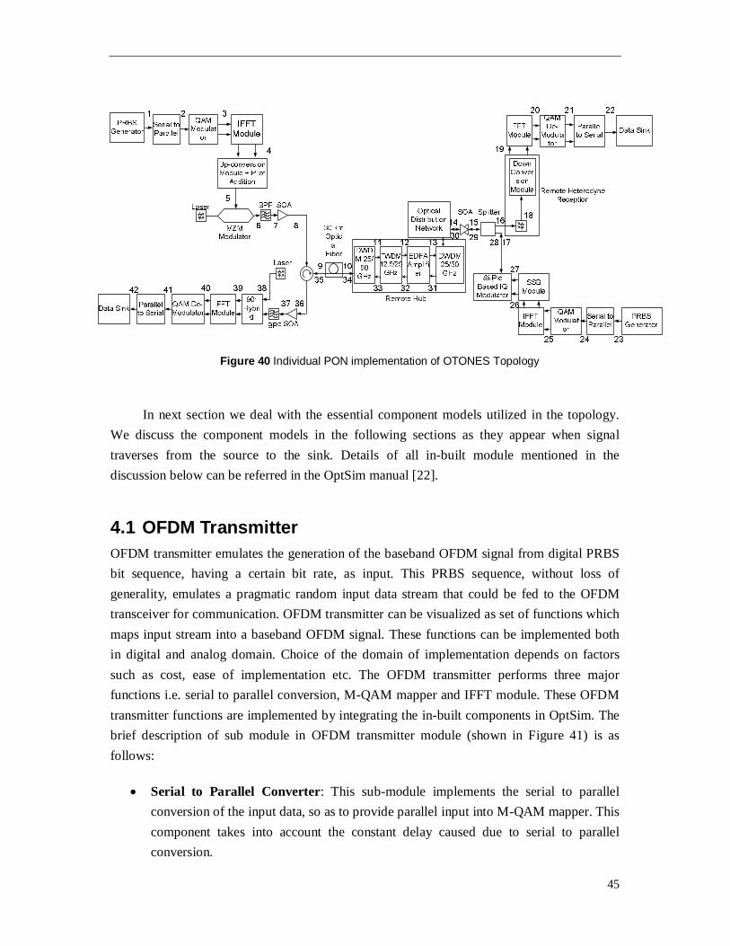
4.1 OFDM Transmitter OFDM transmitter emulates the generation of the baseband OFDM signal from digital PRBS bit sequence, having a certain bit rate, as input. This PRBS sequence, without loss of generality, emulates a pragmatic random input data stream that could be fed to the OFDM transceiver for communication. OFDM transmitter can be visualized as set of functions which maps input stream into a baseband OFDM signal. These functions can be implemented both in digital and analog domain. Choice of the domain of implementation depends on factors such as cost, ease of implementation etc. The OFDM transmitter performs three major functions i.e. serial to parallel conversion, M-QAM mapper and IFFT module. These OFDM transmitter functions are implemented by integrating the in-built components in OptSim. The brief description of sub module in OFDM transmitter module (shown in Figure 41) is as follows:
Serial to Parallel Converter: This sub-module implements the serial to parallel conversion of the input data, so as to provide parallel input into M-QAM mapper. This component takes into account the constant delay caused due to serial to parallel conversion.
Figure 40 Individual PON implementation of OTONES Topology
46
M-QAM Modulator/Mapper: This is one-to-one mapping function which maps input digital bits sequence into a point on constellation in the complex plane. This module takes log 푀 bits and maps them into a particular point in constellation of M points.
IFFT Module: This module performs the inverse fast fourier transform of the input signal into an analog time domain baseband signal. The functionality of DAC is included in this module. The number of subcarrier or to say N points of FFT is limited by the simulation time of the full simulation environment.
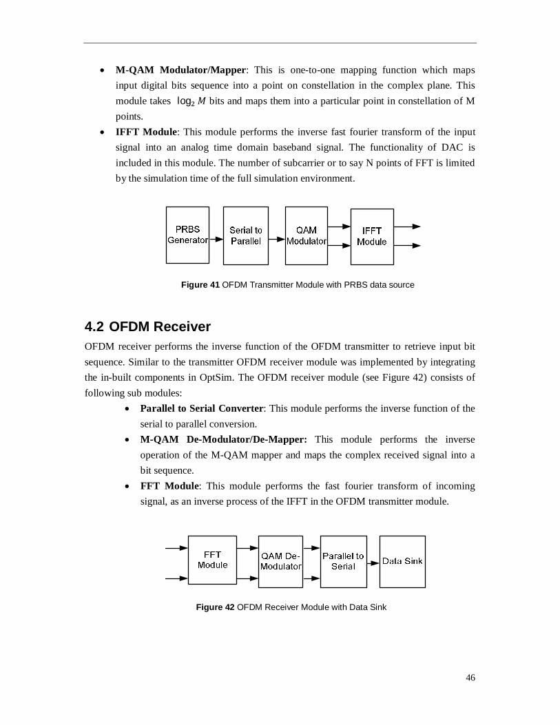
4.2 OFDM Receiver OFDM receiver performs the inverse function of the OFDM transmitter to retrieve input bit sequence. Similar to the transmitter OFDM receiver module was implemented by integrating the in-built components in OptSim. The OFDM receiver module (see Figure 42) consists of following sub modules:
Parallel to Serial Converter: This module performs the inverse function of the serial to parallel conversion.
M-QAM De-Modulator/De-Mapper: This module performs the inverse operation of the M-QAM mapper and maps the complex received signal into a bit sequence.
FFT Module: This module performs the fast fourier transform of incoming signal, as an inverse process of the IFFT in the OFDM transmitter module.
Figure 41 OFDM Transmitter Module with PRBS data source
Figure 42 OFDM Receiver Module with Data Sink

47
4.3 Up-conversion Circuit with Pilot Tone Inclusion This module performs two functions. Firstly the up conversion of the complex incoming signal to a desired microwave frequency referred by 푓 in the thesis and secondly inclusion of pilot tone 푓 . This module includes multiple mixers and amplifiers with the realistic model. Therefore it is essential to discuss the sub-models of mixer and electrical amplifier before discussing this module in detail.
4.3.1 Electrical Amplifier Model In this model, (see Figure 43) the gain and noise characteristics are implemented separately using an ideal amplifier model and additive amplifier noise model. The thermal noise of amplifier has been implemented using the AWGN noise module with noise variance equal to the thermal noise due to the amplifier and is equal to
Noise Variance (휎 ) = 푘 ∙ 푇 ∙ ∆푓 ∙ (푁퐹 − 1) (64)
where k is the Boltzmann constant, 푇 is the ambient temperature , ∆푓 the sampling rate of the signal and NF is the noise figure defined by
푁표푖푠푒 퐹푖푔푢푟푒 (푁퐹) =푆푁푅푆푁푅
(65)
where푆푁푅 and 푆푁푅 are input and output signal to noise ration respectively.
∴ 푁퐹 = ∙∙
(66)
∴ 푁 = 퐺(푁퐹 − 1)푁 (67) where, S is input signal power
푁 is the input thermal power noise power
G is the power gain of the amplifier
푁 is the noise added due to the amplifier
48
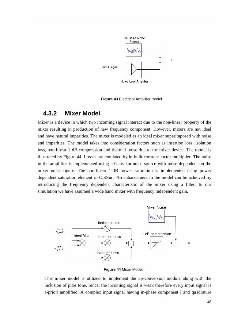
4.3.2 Mixer Model Mixer is a device in which two incoming signal interact due to the non-linear property of the mixer resulting in production of new frequency component. However, mixers are not ideal and have natural imparities. The mixer is modeled as an ideal mixer superimposed with noise and imparities. The model takes into consideration factors such as insertion loss, isolation loss, non-linear 1 dB compression and thermal noise due to the mixer device. The model is illustrated by Figure 44. Losses are emulated by in-built constant factor multiplier. The noise in the amplifier is implemented using a Gaussian noise source with noise dependent on the mixer noise figure. The non-linear 1-dB power saturation is implemented using power dependent saturation element in OptSim. An enhancement in the model can be achieved by introducing the frequency dependent characteristic of the mixer using a filter. In our simulation we have assumed a wide band mixer with frequency independent gain.
This mixer model is utilized to implement the up-conversion module along with the inclusion of pilot tone. Since, the incoming signal is weak therefore every input signal is a-priori amplified. A complex input signal having in-phase component I and quadrature
Figure 44 Mixer Model
Figure 43 Electrical Amplifier model
49
component Q which are multiplied by quadrature tones to produce a real signal. This is followed by addition of a pilot tone and amplification of the outgoing signal as shown in Figure 45.
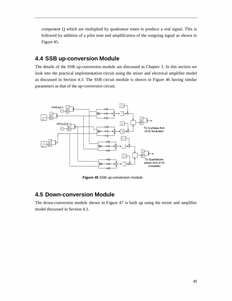
4.4 SSB up-conversion Module The details of the SSB up-conversion module are discussed in Chapter 3. In this section we look into the practical implementation circuit using the mixer and electrical amplifier model as discussed in Section 4.3. The SSB circuit module is shown in Figure 46 having similar parameters as that of the up-conversion circuit.
4.5 Down-conversion Module The down-conversion module shown in Figure 47 is built up using the mixer and amplifier model discussed in Section 4.3.
Figure 45 SSB up-conversion module
50
4.6 Remote Hub based WDM system Details of the WDM system are discussed in Section 2.4 and shown in Figure 48. However, as we know the basic functionality of components of the WDM system can be implemented using filters and combiners with losses. The OTONES envisages two types of WDM components firstly, fractional wavelength division 12.5/25 GHz inter-leaver and secondly dense wavelength division 25/50 GHz inter-leaver.
Figure 46 Up-conversion Circuit with Pilot Tone Addition Module
Figure 47 Down-conversion Module
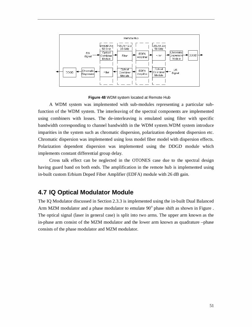
51
A WDM system was implemented with sub-modules representing a particular sub-function of the WDM system. The interleaving of the spectral components are implemented using combiners with losses. The de-interleaving is emulated using filter with specific bandwidth corresponding to channel bandwidth in the WDM system.WDM system introduce imparities in the system such as chromatic dispersion, polarization dependent dispersion etc. Chromatic dispersion was implemented using loss model fiber model with dispersion effects. Polarization dependent dispersion was implemented using the DDGD module which implements constant differential group delay.
Cross talk effect can be neglected in the OTONES case due to the spectral design having guard band on both ends. The amplification in the remote hub is implemented using in-built custom Erbium Doped Fiber Amplifier (EDFA) module with 26 dB gain.
4.7 IQ Optical Modulator Module The IQ Modulator discussed in Section 2.3.3 is implemented using the in-built Dual Balanced Arm MZM modulator and a phase modulator to emulate 90o phase shift as shown in Figure . The optical signal (laser in general case) is split into two arms. The upper arm known as the in-phase arm consist of the MZM modulator and the lower arm known as quadrature –phase consists of the phase modulator and MZM modulator.
Figure 48 WDM system located at Remote Hub
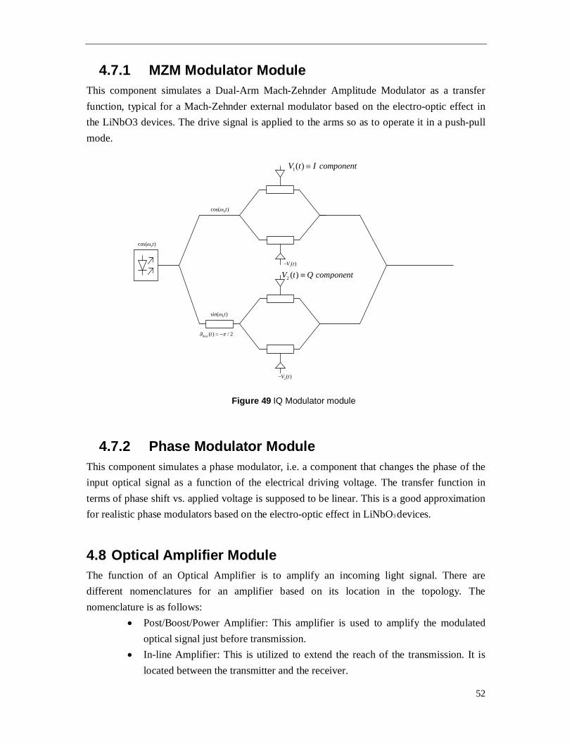
52
4.7.1 MZM Modulator Module This component simulates a Dual-Arm Mach-Zehnder Amplitude Modulator as a transfer function, typical for a Mach-Zehnder external modulator based on the electro-optic effect in the LiNbO3 devices. The drive signal is applied to the arms so as to operate it in a push-pull mode.
4.7.2 Phase Modulator Module This component simulates a phase modulator, i.e. a component that changes the phase of the input optical signal as a function of the electrical driving voltage. The transfer function in terms of phase shift vs. applied voltage is supposed to be linear. This is a good approximation for realistic phase modulators based on the electro-optic effect in LiNbO3 devices.
4.8 Optical Amplifier Module The function of an Optical Amplifier is to amplify an incoming light signal. There are different nomenclatures for an amplifier based on its location in the topology. The nomenclature is as follows:
Post/Boost/Power Amplifier: This amplifier is used to amplify the modulated optical signal just before transmission.
In-line Amplifier: This is utilized to extend the reach of the transmission. It is located between the transmitter and the receiver.
1( ) V t I component
1( )V t
2( )V t
0cos( )t
0cos( )t
0sin( )t
( ) / 2bias t
2 ( ) V t Q component
Figure 49 IQ Modulator module
53
Pre-Amplifier: This amplifier is utilized to amplify a weak received signal before it is detected by a photo-detector.
The optical amplifiers can also be classified on the basis of whether the active region is electrically pumped or optically pumped.
Electrically pumped amplifier: Semi-conductor optical amplifiers (SOA) belong to this category. The population inversion in the active region is achieved by electrical pumping of charges.
Optically pumped amplifier: The amplifiers belonging to this category are rare earth doped amplifier (for instance, EDFA), Fiber Raman Amplifier (FRA) and parametric amplifiers. They rely on the non-linear interaction of the pump and signal. This results in transfer of power from pump to the signal. There is no photon to electron conversion involved in these types of amplifiers.
In our topology, SOA is used as the pre/post amplifier and Erbium doped fiber amplifier as in-line amplifier.
Semiconductor Optical Amplifier Module: The bi-directional operation of the topology requires SOA with bi-directional amplification capabilities. However, the OptSim does not support simulations of closed loop configuration. Therefore, under the assumption that the topology operates well within the linear regime, the bi-directional SOA was modeled as two uni-directional SOAs. As in the linear regime there shall be no interaction between the counter propagating signals.
Erbium Doped Amplifier Module: This in-built module comes in two variants 980 nm pump and 1480 nm pump. The 980 nm pump is characterized by low amplified spontaneous emission and high efficiency. However, 1480 nm pump is characterized by high ASE along with high output power. The 980 nm pump EDFA was utilized as low ASE is advantageous for the topology.
54
5 Results and Discussion In the previous chapters, various aspects relating to the OTONES topology are discussed. In chapter 3 we discussed about various image rejection techniques and select optimal methods for the downstream DS and upstream US signal paths.
In this chapter we present and discuss the results of the simulation of the full concurrent single slice network topology, with inclusion of the schemes established in previous chapters. Based on the results we establish the thresholds for the theoretically optimal operating point of the network shown as in Figure 40, thereby optimizing the system concept.
Before analyzing the simulation results, it is beneficial to understand the key parameters in the network design. Some of the key parameters in the network design are (also shown in Figure 50):
Input Optical Power of Carrier Source: It is defined as the feed-in power of the carrier source of frequency f0 used within a bidirectional concurrent PON.
Central Frequency of DS Filter: It is defined as the mid frequency of the gain response of the filter and corresponds in general to maximum gain value of the response.
Pilot Tone Separation: It is defined as the separation between the pilot tone and its image within the spectra.
Optical Signal to Noise Ratio (OSNR):
푂푆푁푅 =푂푝푡푖푐푎푙 푆푖푔푛푎푙 푃표푤푒푟
푂푝푡푖푐푎푙 푁표푖푠푒 푃표푤푒푟 푤푖푡ℎ푖푛 푟푒푓푒푟푒푛푐푒 푏푎푛푑푤푖푑푡ℎ
Electrical Signal to Noise Ratio (ESNR):
퐸푆푁푅 =퐸푙푒푐푡푟푖푐푎푙 푆푖푔푛푎푙 푃표푤푒푟
퐸푙푒푐푡푟푖푐푎푙 푁표푖푠푒 푃표푤푒푟 푤푖푡ℎ푖푛 푠푖푔푛푎푙 푏푎푛푑푤푖푑푡ℎ
It is essential to establish a Figure of Merit (FOM) to evaluate the performance of the network with respect to the parameters discussed above. It has now been established that Error Vector Magnitude (EVM) is a good FOM for complex modulation formats based OFDM signals. Therefore, we choose EVM as the FOM criterion for our network analysis.
Error Vector Magnitude is defined by:
퐸푉푀 =∑ 퐷푆
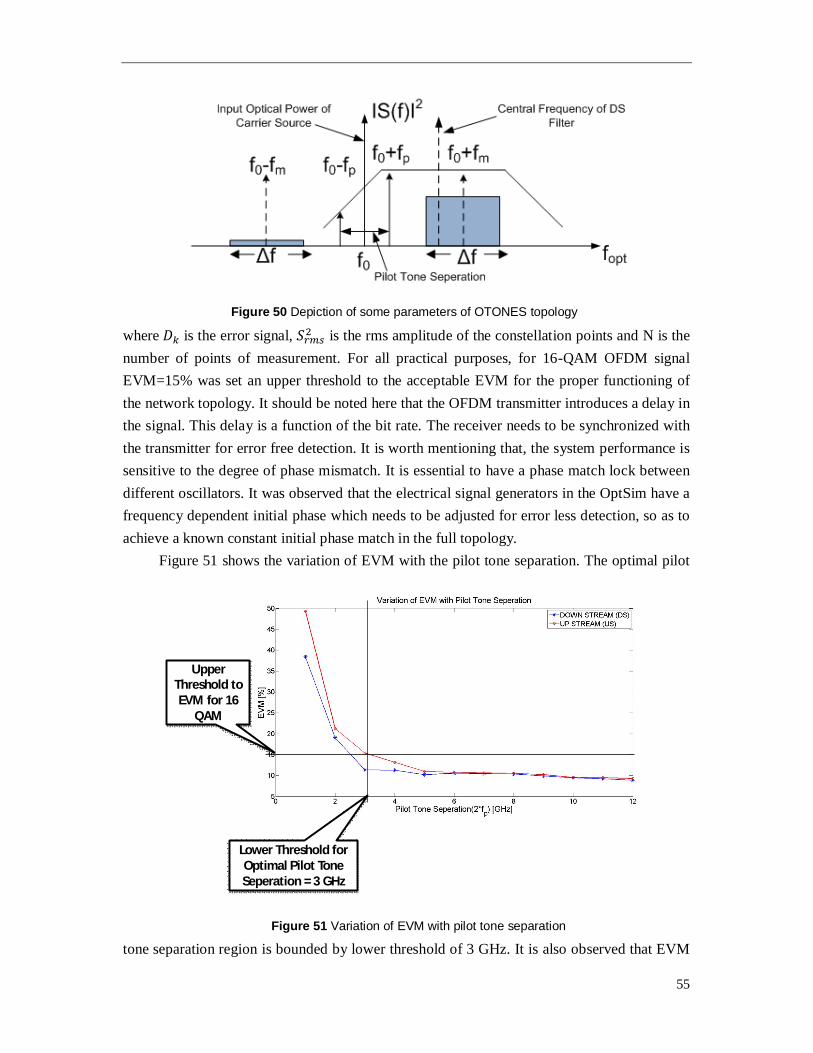
55
where 퐷 is the error signal, 푆 is the rms amplitude of the constellation points and N is the number of points of measurement. For all practical purposes, for 16-QAM OFDM signal EVM=15% was set an upper threshold to the acceptable EVM for the proper functioning of the network topology. It should be noted here that the OFDM transmitter introduces a delay in the signal. This delay is a function of the bit rate. The receiver needs to be synchronized with the transmitter for error free detection. It is worth mentioning that, the system performance is sensitive to the degree of phase mismatch. It is essential to have a phase match lock between different oscillators. It was observed that the electrical signal generators in the OptSim have a frequency dependent initial phase which needs to be adjusted for error less detection, so as to achieve a known constant initial phase match in the full topology.
Figure 51 shows the variation of EVM with the pilot tone separation. The optimal pilot
tone separation region is bounded by lower threshold of 3 GHz. It is also observed that EVM
Figure 50 Depiction of some parameters of OTONES topology
Figure 51 Variation of EVM with pilot tone separation
Upper Threshold to EVM for 16
QAM
Lower Threshold for Optimal Pilot Tone Seperation = 3 GHz
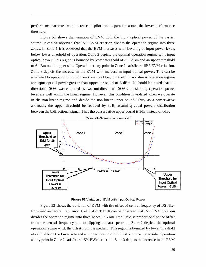
56
performance saturates with increase in pilot tone separation above the lower performance threshold.
Figure 52 shows the variation of EVM with the input optical power of the carrier source. It can be observed that 15% EVM criterion divides the operation regime into three zones. In Zone 1 it is observed that the EVM increases with lowering of input power levels below lower threshold of operation. Zone 2 depicts the optimal operation regime w.r.t input optical power. This region is bounded by lower threshold of -9.5 dBm and an upper threshold of 6 dBm on the upper side. Operation at any point in Zone 2 satisfies < 15% EVM criterion. Zone 3 depicts the increase in the EVM with increase in input optical power. This can be attributed to operation of components such as fiber, SOA etc. in non-linear operation regime for input optical power greater than upper threshold of 6 dBm. It should be noted that bi-directional SOA was emulated as two uni-directional SOAs, considering operation power level are well within the linear regime. However, this condition is violated when we operate in the non-linear regime and decide the non-linear upper bound. Thus, as a conservative approach, the upper threshold be reduced by 3dB, assuming equal powers distribution between the bidirectional signal. Thus the conservative upper bound is 3dB instead of 6dB.
Figure 53 shows the variation of EVM with the offset of central frequency of DS filter from median central frequency 푓 =193.427 THz. It can be observed that 15% EVM criterion divides the operation regime into three zones. In Zone 1the EVM is proportional to the offset from the central frequency due to clipping of data spectrum. Zone 2 depicts the optimal operation regime w.r.t. the offset from the median. This region is bounded by lower threshold of -2.5 GHz on the lower side and an upper threshold of 0.5 GHz on the upper side. Operation at any point in Zone 2 satisfies < 15% EVM criterion. Zone 3 depicts the increase in the EVM
Figure 52 Variation of EVM with Input Optical Power
Upper Threshold to EVM for 16
QAM
Lower Threshold for Input Optical
Power = -9.5 dBm
Upper Threshold for Input Optical
Power = 6 dBm
Zone 1 Zone 2 Zone 3
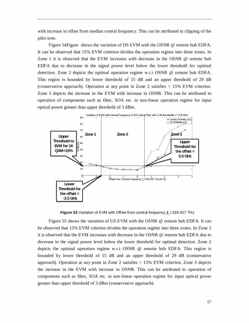
57
with increase in offset from median central frequency. This can be attributed to clipping of the pilot tone.
Figure 54Figure shows the variation of DS EVM with the OSNR @ remote hub EDFA. It can be observed that 15% EVM criterion divides the operation regime into three zones. In Zone 1 it is observed that the EVM increases with decrease in the OSNR @ remote hub EDFA due to decrease in the signal power level below the lower threshold for optimal detection. Zone 2 depicts the optimal operation regime w.r.t OSNR @ remote hub EDFA. This region is bounded by lower threshold of 15 dB and an upper threshold of 29 dB (conservative approach). Operation at any point in Zone 2 satisfies < 15% EVM criterion. Zone 3 depicts the increase in the EVM with increase in OSNR. This can be attributed to operation of components such as fiber, SOA etc. in non-linear operation regime for input optical power greater than upper threshold of 3 dBm.
Figure 55 shows the variation of US EVM with the OSNR @ remote hub EDFA. It can be observed that 15% EVM criterion divides the operation regime into three zones. In Zone 1 it is observed that the EVM increases with decrease in the OSNR @ remote hub EDFA due to decrease in the signal power level below the lower threshold for optimal detection. Zone 2 depicts the optimal operation regime w.r.t OSNR @ remote hub EDFA. This region is bounded by lower threshold of 15 dB and an upper threshold of 29 dB (conservative approach). Operation at any point in Zone 2 satisfies < 15% EVM criterion. Zone 3 depicts the increase in the EVM with increase in OSNR. This can be attributed to operation of components such as fiber, SOA etc. in non-linear operation regime for input optical power greater than upper threshold of 3 dBm (conservative approach).
Figure 53 Variation of EVM with Offset from central frequency 풇풄=193.427 THz
Upper Threshold to EVM for 16 QAM=15%
Lower Threshold for the offset =
-2.5 GHz
Upper Threshold for the offset =
0.5 GHz
Zone 1 Zone 2 Zone 3
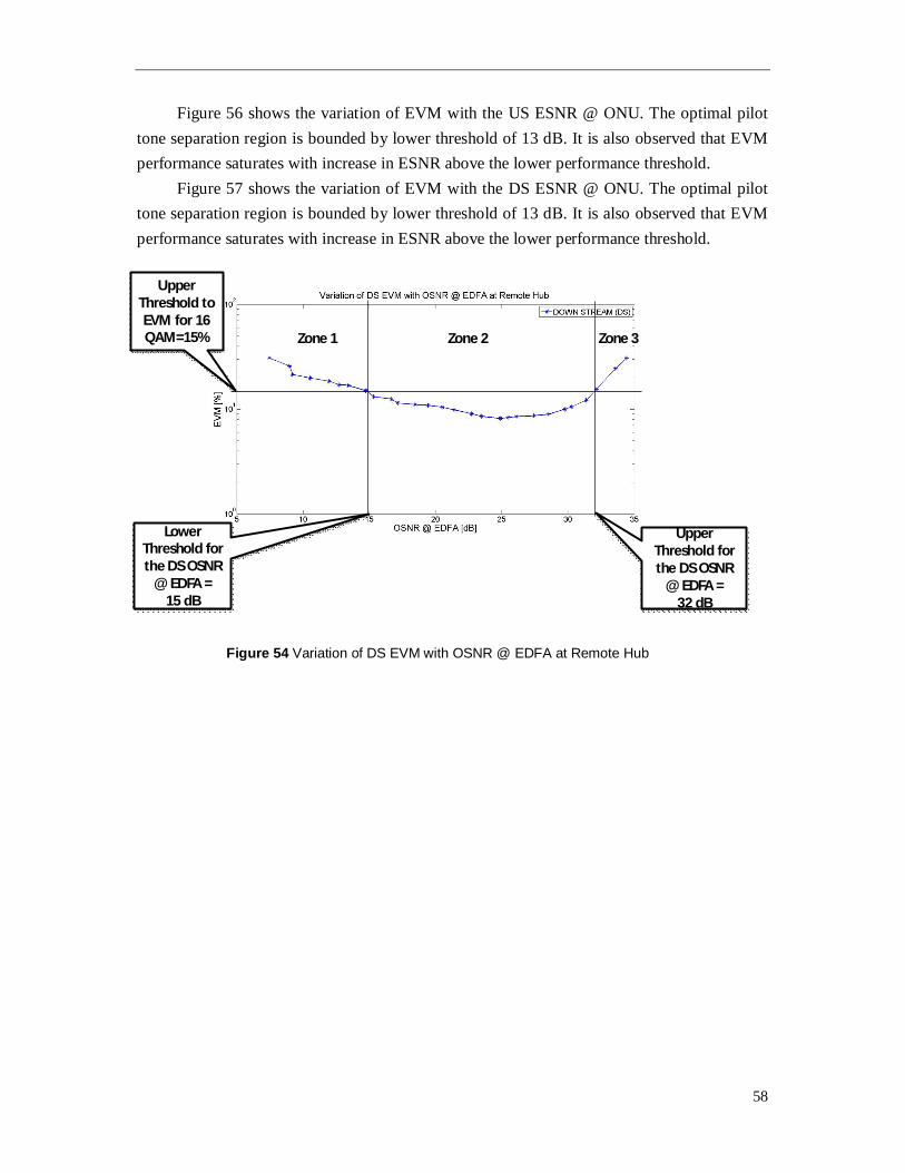
58
Figure 56 shows the variation of EVM with the US ESNR @ ONU. The optimal pilot tone separation region is bounded by lower threshold of 13 dB. It is also observed that EVM performance saturates with increase in ESNR above the lower performance threshold.
Figure 57 shows the variation of EVM with the DS ESNR @ ONU. The optimal pilot tone separation region is bounded by lower threshold of 13 dB. It is also observed that EVM performance saturates with increase in ESNR above the lower performance threshold.
Figure 54 Variation of DS EVM with OSNR @ EDFA at Remote Hub
Upper Threshold to EVM for 16 QAM=15%
Lower Threshold for the DS OSNR
@ EDFA =15 dB
Upper Threshold for the DS OSNR
@ EDFA = 32 dB
Zone 1 Zone 2 Zone 3
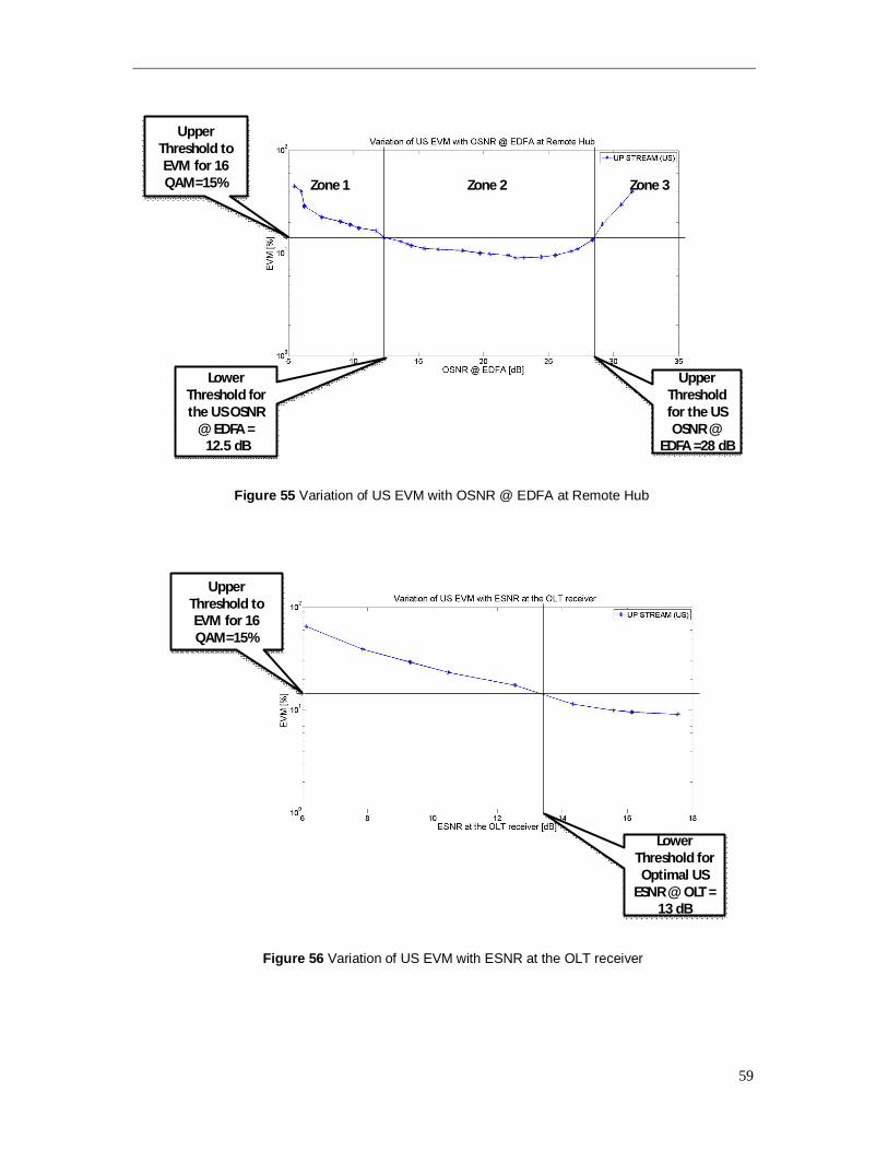
59
Figure 55 Variation of US EVM with OSNR @ EDFA at Remote Hub
Upper Threshold to EVM for 16 QAM=15%
Lower Threshold for the US OSNR
@ EDFA =12.5 dB
Upper Threshold for the US OSNR @
EDFA =28 dB
Zone 1 Zone 2 Zone 3
Figure 56 Variation of US EVM with ESNR at the OLT receiver
Upper Threshold to EVM for 16 QAM=15%
Lower Threshold for Optimal US
ESNR @ OLT = 13 dB
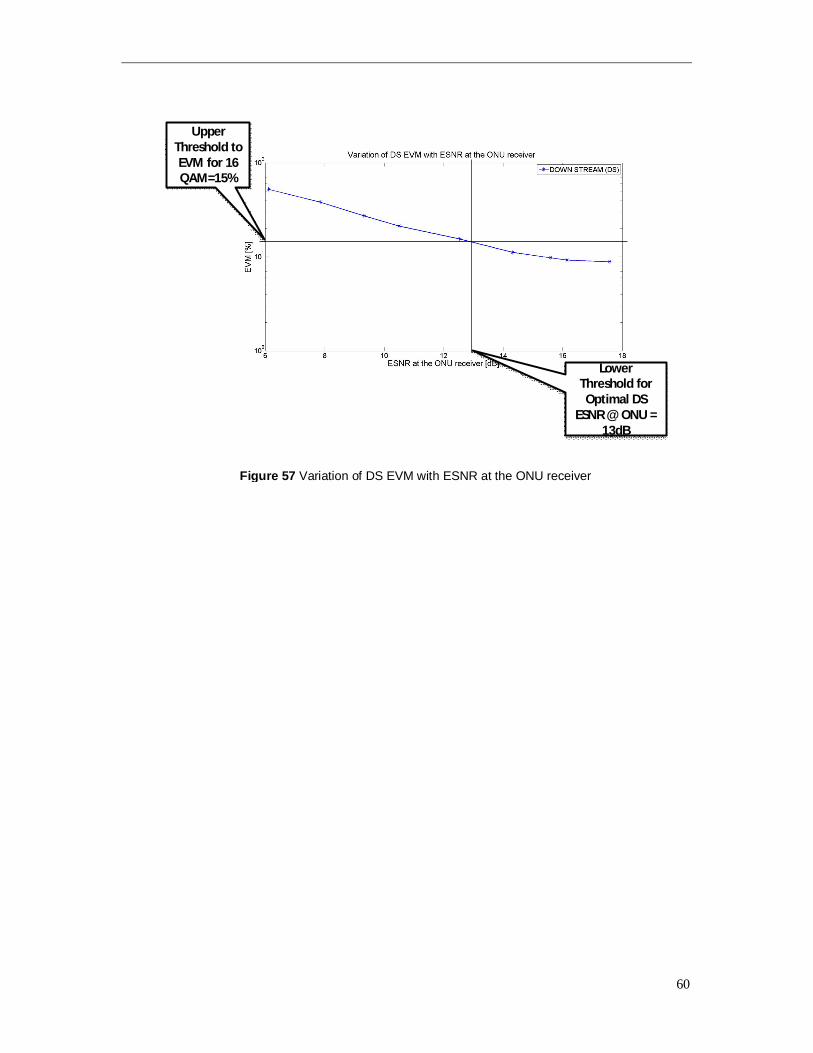
60
Figure 57 Variation of DS EVM with ESNR at the ONU receiver
Upper Threshold to EVM for 16 QAM=15%
Lower Threshold for Optimal DS
ESNR @ ONU = 13dB
61
6 Conclusion and Outlook In this thesis, theoretical investigation of OFDM based optical access network topology is carried out as a part of the EU FP7 project OTONES. The thesis provides an in depth view of the various aspects of the topology and formulates its key requirements. The thesis also explores the fundamentals of the varied state of the art technologies which are utilized in the novel topology.
However, the investigation was primarily focused on two important aspects of the topology. Firstly, finding the optimal analog circuitry for the ONU and secondly, finding the optimal operation regime for the topology and hence optimizing the system level concept. The requirement for an analog circuitry emerged from the fact that the topology implements the “PUDG” spectral design. It is characterized by a recurrent spectral slot sequence of pilot (P), upstream data (U), downstream data (D) and guard band (G) sections. This necessitates the up-conversion of both DS and US data to the appropriate slot. This up-conversion is then followed by up-conversion of full “PUDG” slice to optical domain for transmission. The successive translations to higher frequencies results in a redundant image spectrum reducing spectral efficiency by 3 dB.
In this thesis, the SSB generation methods for image rejection are discussed. Novel Bedrosian method based on Bedrosian theorem is established as a promising method for image rejection. We show that this method is an analog implementation of the Hilbert Transform method and does not involve any approximation. All the methods are then evaluated based on the criterion established for OTONES topology.
It was found that, optical filtering achieves ~ 28 dB suppression depth along with ensuring minimum implementation complexity and phase distortion for pilot tone inclusion. Thus for the DS path, optical filtering is considered a reasonable option. The Novel Bedrosian method is characterized by achievable suppression depth of 30 dB, spectral power saving by 3dB, low phase distortion and lower implementation complexity as compared to its digital counterpart. Thus, Novel Bedrosian method which is based on the Bedrosian Theorem is proposed for the US path. The tolerance limits for this method, with 10 dB depression in suppression depth as FOM, were established for its physical implementation. In order to meet the tolerance criterion, phase mismatch of less than 0.22 radians and arm imbalance of 0.78 V were considered desirable.
After establishing optimal analog circuitry, the full concurrent topology was simulated to find the optimal operation regime. The simulations were conducted as an iterative process. It can be concluded that, the optimal operation regime is as follows:
Input Optical Power 휖 [-10 dBm 3 dBm] Pilot Tone Seperation > 3 GHz Offset from central frequency i.e. 193.427 THz 휖 [-2.5 GHz 0.5 GHz] OSNR for DS @ EDFA of Remote Hub 휖 [15 dB 32 dB]
62
OSNR for US @ EDFA of Remote Hub 휖 [12.5 dB 28 dB] ESNR for DS signal > 13 dB ESNR for US signal > 13 dB
Operation within the optimal regime ensures adherance to less than 15% EVM criterion for both US and DS path. Finally as a key feature of the thesis, we optimize the system level concept by the use of the proposed Novel Bedrosian Method as the optimal analog circuitry for OTONES topology and provide a region of optimal operation of the topology.
Since all slices (slice is 12.5 GHz band per PON) have an identical topological setup. Therefore, in this thesis, without loss of generality we had considered single slice simulations for finding optimal analog circuitry and optimizing the system level concepts per slice. However, as the logical next step simulation full network with multi slice and multi wavelength consideration is proposed. In this thesis, we have discussed the problem of image spectra and methods to mitigate it. However, further analysis of the impact of insufficient suppression of the image spectra on other wavelength channels shall assist in designing the wavelength channels in the topology along with establishing more stringent tolerance criterion for the methods. Last but not the least, is the experimental validation of the OTONES topology.
63
Bibliography [1] Abbas, G. L., S., C. V.W., y Yee, T. K., "Local-oscillator Excess Noise Suppression for
Homodyne and Heterodyne Detection," Optics Letters, p. 8(8): 419–421, 1983 [2] Anis Rehman, Ph.D, “A Review of DWDM- The Heart of Optical Network”[Online].
Available: http://arphotonics.net/DWDM_Review.pdf [3] H. Sari et al.," Transmission Techniques for Digital Terrestrial TV Broadcasting," IEEE
Comm. Mag., vol. vol. 33, pp. no. 2, pages 100–109, February 1995 [4] Ove Edfors et al.," An Introduction to Orthogonal Frequency-Division Multiplexing,"
Research 101 Report, no. 1996:16, Division of Signal Processing, Lulea University of Technlogy, Sweden, September 1996.
[5] Bar-David I., Saltz J., "On dual Optical detection: Homodyne and retransmitted reference heterodyne detection," IEEE Trans. Commun., vol 36, pp. pp.1309-1315, Dec. 1988
[6] Barry R.J., Lee E.A., "Performance of Coherent Optical Receivers," Proceedings of the IEEE, vol. vol. 78, pp. no. 8, pp. 1369-1394, August 1990
[7] D. Matic, OFDM Synchronization and Wideband Power Measurements at 60 GHz for Future Wireless Broadband Multimedia Communications, September 2001: Ph.D. Thesis, Aalborg University.
[8] E. Bedrosian, "A Product Theorem for Hilbert Transform," Rand Corporation Memorandum, no. RM-3439-PR, December, 1962.
[9] E. Desurvire, Wiely Survival Guide in Global Telecommunications, Signaling Principles, Wiley 2004.
[10] Esdras Anzuola Valencia, “Digital coherent transceiver for optical communications. From Design to Implementation”, Department of Communication and Signal Theory Technical University of Catalonia (UPC), February 2012
[11] G. Agrawal, " Fiber-Optic Communication Systems"", Wiley Series 1997
[12] Garret, I., Bond, J., J., W., D., L., y G., J., "Impact of Phase Noise in Weakly Coherent Systems:a New and Accurate Approach," Journal of Lightwave Technology, p. 8(4): 329–337,1990.
[13] H. Grießer, M. Eiselt, B. Teipen, A. Autenrieth, K. Grobe, J.-P. Elbers, “Options for Tb/s,” in ITG workshop 3.5.1, Karlsruhe, Nov. 2011
[14] Wikipedia, Bessel Filter [Online]. Available: http://en.wikipedia.org/wiki/Bessel_filter [15] Filter Design [Online]. Available: http://www.dsplog.com/ [16] OTONES Concept Paper [Online]. Available:
http://www.ipq.kit.edu/research/projects/OTONES/publications/2011/D7.1%20- %20Concept-Paper.pdf
[17] Fiber Types in Gigabit Optical Communications [Online]. Available: http://www.cisco.com/en/US/prod/collateral/modules/ps5455/white_paper_c11- 463661.html
[18] J. Leuthold, "Optical Communication Systems - Part 2: Transmitter and Receiver Formats", IPQ,Karlsruhe Institute of Technology, WS 2011/2012.
[19] J. Salz, “Modulation and detection for coherent lightwave communication systems,” IEEE Comun. Mag., vol. vol 24, pp. pp.38-49, 1986.
[20] M. Seitzmetz, “Höherwertige Modulationsverfahren für die Glasfaserübertragung – System,” in Proc. ITG Tagung – Photonische Netze, Leipzig 2009.
[21] Nicola Marchetti, Muhammad Imadur Rahman, Sanjay Kumar, and Ramjee Prasad,
64
“OFDM: Principles and Challenges”, Springer Science Business Media, LLC 2009 [22] OptSim Guide: Sample Mode Reference [23] R. N. a. R. Prasad, OFDM for Wireless Multimedia Communications, Norwood, MA,
USA, 2000: Artech House. [24] Telecordia documents: GR-1209-CORE; FOTP-205
[25] U. Gliese, S. Nørskov, and T. N. Nielsen, “Multifunctional Fiber-Optic Microwave Links Based on Remote Heterodyne Detection,” IEEE TRANSACTIONS ON MICROWAVE THEORY AND TECHNIQUES, Vols. VOL. 46, NO. 5, MAY 1998.
[26] U. Jha, Low Complexity Resource Efficient OFDM Based Transceiver Design, Denmark: Ph.D. Thesis, Aalborg University, September 2002.
[27] Weaver D.K. “A Third Method of Generation and Detection of Single-Sideband Signals”, Single Sideband Issue Proceedings of the IRE

65
Appendix: List of Abbreviations ADC Analog to Digital Converter ASK Amplitude Shift Keying AWG Arrayed Waveguide BPSK Binary Phase Shift Keying CMRR Common Mode Rejection Ratio CP Cyclic Prefix CW Continuous Wave D/A Digital to Analog DAC Digital to Analog Converter dB Decibel DFT Discrete Fourier Transform DQPSK Differential Quadrature Phase Shift Keying DMUX De-Multiplexer DPSK Differential Phase Shift Keying DS Down Stream DWDM Dense Wavelength Division Multiplexing EDFA Erbium Doped Fiber Amplifier EO Electro-optic ESNR Electrical Signal to Noise Ratio FDM Frequency Division Multiplexing FEC Forward Error Correction FFT Fast Fourier Transform FTTH/B Fiber-To-The-Home/Building FWDM Fractional Wavelength Division Multiplexing GBPS Giga Bits Per Second GHz Giga Hertz I In-Phase ICI Inter Carrier Interference IDFT Inverse Discrete Fourier Transform I.F. Intermediate Frequency IFFT Inverse Fast Fourier Transform ISI Inter Symbol Interference ITU International Telecommunication Union LPF Low Pass Filter LSB Lower Side Band MZI Mach-Zehnder Interferometer MUX Multiplexer
66
OCX Optical Cross connect Switches OTONES OFDM based optical access network topology OLT Optical Line Terminal ONU Optical Network Unit OPSD Optical Power Spectral Density OSNR Optical Signal to Noise Ratio PAPR Peak to Average Power Ratio PAM Pulse Amplitude Modulation PDL Polarization Dependent Losses P2MP Point to Multi Point PON Passive Optical Network PRBS Pseudo Random Bit Sequence PSD Power Spectral Density PSK Phase Shift Keying P.V. Principal Value QAM Quadrature Amplitude Modulation Q Quadrature Phase QPSK Quadrature Phase Shift Keying RF Radio Frequency SSB SC Single Side Band Subcarrier Suppression SC BW Sub Carrier Bandwidth SOA Semiconductor Optical Amplifier SPT Spectral Propagation Technique SSB Single Side Band USB Upper Side Band US Up Stream VBS Variable Bandwidth Simulations