Embed Size (px)
Citation preview

Theoretical Study of Electronic and Optical Properties in Doped Quantum Structureswith Razavy Confining Potential: Effects of External Fields
Hassen Dakhlaoui1,2, J. A. Gil-Corrales3, A. L. Morales3, E. Kasapoglu4, A. Radu5,
R. L. Restrepo6, V. Tulupenko3, J. A. Vinasco3, M. E. Mora-Ramos7, and C. A. Duque3∗1Nanomaterials Technology unit, Basic and Applied Scientific Research Center (BASRC),
College of Science of Dammam, Imam Abdulrahman Bin Faisal University,P. O. Box 1982, 31441 Dammam, Saudi Arabia
2Department of Physics, College of Sciences for Girls,Imam Abdulrahman Bin Faisal University, Saudi Arabia
3Grupo de Materia Condensada-UdeA, Instituto de Fısica, Facultad de Ciencias Exactas y Naturales,Universidad de Antioquia UdeA, Calle 70 No. 52-21, Medellın, Colombia
4Faculty of Science, Department of Physics, Sivas Cumhuriyet University, 58140 Sivas, Turkey5Department of Physics, “Politehnica” University of Bucharest, 313 Splaiul Independen tei, 060042 Bucharest
6Universidad EIA, Envigado 055428, Colombia and7Centro de Investigacion en Ciencias-IICBA, Universidad Autonoma del Estado de Morelos,
Av. Universidad 1001, Cuernavaca 62209, Morelos, Mexico(Dated: September 8, 2021)
We investigate the energy states of confined electrons in doped quantum structures with Razavy-like confining potentials. The theoretical investigation is performed within the effective mass andparabolic band approximations, including the influence of externally applied electric and magneticfields. First, we analyze the case of a Razavy quantum well and determine its conduction subbandspectrum, focusing on the lowest energy levels and their probability densities. These propertieshave been numerically determined by self-consistently solving the coupled system of Schrodinger,Poisson, and charge neutrality equations. Doping is introduced via an on-center δ-like layer. Inorder to evaluate the associated total (linear plus nonlinear) optical absorption coefficient (TOAC),we have calculated the corresponding diagonal and off-diagonal electric dipole matrix elements, themain energy separation, and the occupancy ratio which are the main factors governing the variationof this optical response. A detailed discussion is given about the influence of doping concentration aswell as electric and magnetic fields, which can produce shifts in the light absorption signal, towardseither lower or higher frequencies. As an extension of the self-consistent method to a two-dimensionalproblem, the energy states of quantum wire system of circular cross section, with internal dopingand Razavy potential have been calculated. The response of eigenvalues, self-consistent potentialsand electron densities is studied with the variation of δ-doping layer width and of the donor density.Finally, the origin of Friedel-like oscillations, that arise in the density profile, generated by theoccupation of internal and surface electronic states has been explained.
I. INTRODUCTION
Semiconductor structures based on quantum wells(QWs), quantum-well wires , and quantum dots haveacquired a huge importance in the process of designinglow-dimensional devices, mostly due to their features ofcharge carriers confinement. To satisfy the exigence re-quired by new generation of optoelectronic devices, theinvolved semiconductor structures must be suitably se-lected upon the basis of their confinement potential ge-ometry, their dimensions, and the possible influence ofcertain external physical factors. Among these factors,we can cite the insertion of delta doped layers, as well asthe application of either nonresonant intense laser fieldradiation, electric fields, magnetic fields, or a combina-tion of these probe fields. All of them would play a crucial
∗Corresponding author (C. A. Duque): [email protected]
role in tuning the energy spectrum of the confined carrierstates [1–10].
As it is well known, the application of an external elec-tric field leads to a tilt of the confining potential andpushes the electron wave functions towards the edge ofthe structure, producing a significant change in the en-ergy levels and, per consequent, in the transition ener-gies. This, in turn, produces noticeable modificationsin the optical absorption response of the system. Theapplication of a magnetic field provides an additionalparabolic confinement that causes further spatial spreadin the wave functions so that affecting the dipole matrixelements. The influences of both electric and magneticfields have been theoretically and experimentally studiedby many researchers [11–21]. For instance, Dakhlaouiet al., investigated the effects of magnetic and electricfields on the TOAC [22]. They showed that these probescan control the red and blue shifts of the TOAC in dou-ble and triple δ-doped GaAs semiconductor heterostruc-tures. Ungan et al. reported on the optical responses

2
in hyperbolic-like QWs under external electric and mag-netic fields [23]. They demonstrated that the TOACand the total relative refractive index change coefficientcan be shifted towards the blue or the red by adjust-ing the applied field intensities. The impacts of externalperturbations on the optical and magnetic properties ofGaAs/AlGaAs semi-parabolic QW have been widely dis-cussed and commented by Hien et al. [24]. They provedthat the magneto-optical properties are largely affectedby the external fields.
Besides the application of external fields, the δ−dopingtechnique represents an ultimate concept in semiconduc-tor’s processing [25–31]. It is proved among the last yearsthat this method is highly practical to adjust the energylevels in order to obtain the desired electronic mobilityand optical absorption. For instance, in GaAs-based sys-tems, the most typical n-type δ−doping technique con-sists of inserting a thin layer containing silicon atoms.Once these atoms are ionized, they supply additional freeelectrons into the system. In addition, the silicon layercreates a triangular-shaped quantum well which wouldaffect the spatial spread of the wave functions and furnishfurther confinement to the carriers [32, 33]. Various re-search works have explored, both experimentally and the-oretically, the impact of δ-doping on the behavior of theTOAC in semiconductor quantum nanostructures [34–41]. For instance, Gaggero-Sager et al. studied the ef-fects of temperature on the energy levels in a single dopedQW [42], whereas Dhafer et al. showed the importance ofan inserted δ-InGaAs layer in a single AlxGayIn1−x−yAsQW. They found that the inserted layer can improve theintensity of the optical gain which is a requirement forfiber-optical communications [43]. J. Osvald studied theeffect of a non-central δ-doping layer on the energy levelsand electronic density in GaAs QWs [44]. On the otherhand, in 1980 M. Razavy used double potential wells inthe quantum theory of molecules to describe the motionof a particle in the presence of two force fields [45]. Thesetypes of potentials are known today as Razavy potentials[46, 47], and are used as a model to describe the couplingof two molecules or quantum dots [48–51]. Effects of in-tense laser field and position dependent effective mass inRazavy QWs (Razavy-like quantum wells) were investi-gated in Ref. [52]. In their works, these authors haveshown that the intensity of the TOAC can be largelytuned by varying the ionized impurity concentration inthe doping layer.
Another class of heterostructures that can be studiedby a similar procedure are quantum wires (QWRs), whichare semiconductor structures in which electrons are con-fined in the transverse plane and therefore can only movein one dimension. A consequence of the above is that theelectronic energy levels present a discrete behavior alongthe cross section of the structure, while in the free dimen-sion the electrons present a continuous spectrum. QWRshave been the subject of study for more than 40 years,as noticed -for example- from a bunch of early references[53–57]. Due to the remarkable applications of this type
of low-dimensional structures in areas as diverse as flex-ible electronics (when designing thin-film transistors) orhigh-efficiency solar cells [58], among others; to seek animprovement in the properties of electronic conductionwould become a boost to development and characteriza-tion of this type of systems. In recent years, results ofgreat interest have been reported along these lines, someof which have appeared in references [59–62].
Motivated by all the cited works, here we aim to inves-tigate the effects of the concentration of an on-center thindoping layer and of externally applied electric and mag-netic fields on the TOAC in Razavy-like GaAs quantumstructures. We shall study the impact of these param-eters on the lowest energy separations, the occupancyratios, and dipole matrices which are preponderant fac-tors governing the TOAC variation. In the first partwe develop the one-dimensional problem of a GaAs δ-doped QW (with z-oriented growth direction) having aRazavy-type confinement potential. For this system, theconfined electronic states are calculated, as well as theself-consistent potentials, with a special care taken on de-termining the Fermi level position, affected by the bothtemperature and ionized impurity distribution. Subse-quently, external electric and magnetic fields are appliedin order to analyze the variations in obtained results andfinally the optical absorption response is investigated.The second problem dealt with is a two-dimensional sys-tem corresponding to a GaAs QWR with circular crosssection and exposed borders (the confinement plane hasbeen taken as xy), with an additional δ-type doping andan inner Razavy-like potential. The problem for the elec-tron energy states in this case is also solved in a self-consistent way, taking into account a fundamental differ-ence: In this case the Fermi level is no longer modifiedby the density of donors because the system has exposedborders. So, a “Fermi Level Pinning” is presented whichkeeps it fixed. Another fundamental difference with re-spect to the QW structure is that, in this type of systems,variations in the electron density profile known as Friedeloscillations can occur at low temperatures. To study thisparticular phenomenon, electron states in this system hasbeen calculated for T = 10 K and not at 300 K as thefirst problem. In this second case, the electronic states,self-consistent potential and electron density have beencalculated for different widths of the δ-layer, with differ-ent concentrations. Self-consistent procedures have beenperformed by numerically solving the effective mass con-duction band equation using the finite element method(FEM). In accordance, this work is organized as follows:in sections 2 we outline the theoretical equations andthe method of resolution for the one-dimensional systemquantum well and the quantum wire system with exposedboundaries. The discussion and comments on the ob-tained results for each system are presented in section 3,while the conclusions are given in section 4.

3
II. THEORETICAL FRAMEWORK
A. Razavi quantum-well (quantum well withRazavy-like potential)
-10 -5 0 5 100
100
200
300
400
500
ener
gy (m
eV)
z (nm)
y
xA = 2M = 3
V(z) = V0 [ A cosh(z/d) - M ] 2
FB
z
dope
d la
yer
FIG. 1: (color online) Schematic representation of dopedRazavy quantum well under applied electric and magneticfields.
The problem under consideration here consists of aGaAs conduction electron that moves under the influ-ence of an on-center doped Razavy-like QW potentialand undergoes the effect of external electric and mag-netic fields. The electric field is assumed to be orientedalong the z-growth direction and the magnetic field is ap-plied perpendicular to the electric field, and lies withinthe plane of the layers. In Fig. 1 we plot a Razavy-likeconfining profile, together with a schematic representa-tion of the n-type doped layer. The δ-parameter (2-nm inthis work) corresponds to the finite width of the on-centerdoped layer, which has a two-dimensional Nd concentra-tion of ionized donor atoms. Within the effective massand parabolic band approximations, the Hamiltonian fora confined electron is given by [1]:
H =1
2m∗
[~p+
e
c~A(~r)
]2+ Vc(z) + VH(z) + e F z , (1)
where c, e, and m∗ denote the speed of light in the vac-uum, the absolute value of the elementary charge, and theelectron effective mass, respectively. Additionally, ~p rep-resents the momentum operator, and F is the intensity of
the applied electric (~F ). Within the Landau gauge, thevector potential associated to the applied magnetic field
( ~B) is given by ~A(~r) = B z x (B stands for the magneticfield intensity). Furthermore, VH(z) is the Hartree po-tential, which represents the additional conduction bandreshaping due to the presence of the low-dimensional elec-tron gas that arises from the donor ionization in the δ-layer. Besides, Vc(z) is the Razavy-like confining poten-tial given by [52]:
Vc(z) = V0
[A cosh
( zD
)−M
]2, (2)
where a set of parameters with V0 = 228 meV, A = 2,
M = 3, D =Leff
3 , and Leff = 20 nm (the total width ofthe QW) has been chosen for the calculation.
The wave function associated to the Hamiltonian inEq. (1) can be written as [63]:
ψ (~r) = exp(i ~k⊥ · ~ρ) Φ′(z) , (3)
where ~k⊥ = (kx, ky), ~ρ = (x, y), and Φ′(z) satisfies thefollowing differential equation [63]:
H0 Φ′ (z) =
(Ez −
~2 k2y2m∗
)Φ′ (z) . (4)
where
H0 = − ~2
2m∗d2
dz2+e2B2
2m∗
(z +
~ kxeB
)2
+e F (z + Leff/2) + VH (z) . (5)
The z-component of the Eq. (4) can be written in theform [63]:
H Φ (z) = Ez Φ (z) . (6)
where
H = − ~2
2m∗d2
dz2+e2B2
2m∗z2
+e F (z + Leff/2) + VH (z) . (7)
Note that the solutions of Eq. (6) correspond to the bot-tom of the confined conduction subbands, i.e., (kx, ky) =(0, 0).
The calculation of the Fermi level (EF ) is based on thecharge neutrality condition, such that the total numberof electrons must be equal to the total number of ionizeddonors per unit area (assuming that all the silicon atomsare ionized)
nd =∑i
m∗ kB T
π ~2log
[1 + exp
(EF − EikB T
)], (8)
where kB is the Boltzmann constant and T (= 300 K inthis work) denotes the absolute temperature.
The Hartree potential VH (z) which describes the elec-trostatic interaction of electrons and ionized ions resultsfrom the solution of the generalized Poisson equation [64]:
d2VH (z)
dz2=
e2
ε ε0[nd (z)− n (z)] , (9)
where ε (ε0) is the GaAs (vacuum) static dielectric con-stant and nd is the 3D donor density in the delta layer.Also, in Eq. (9)
n(z) =∑i
m∗ kB T
π ~2log
[1 + exp
(EF − EikB T
)]Φ2i (z) ,
(10)
4
The Eqs. (6-9) are discretized using the finite differ-ence method (FDM) and solved iteratively. Under sucha procedure, the Schrodinger and Poisson equations arethen changed to matrices of type Ax = λx and B x = ρ,respectively. Here, λ represents the energy and x is a col-umn wave vector describing the electron wave function.After computing the energy levels and their correspond-ing wave functions, the linear, third-order nonlinear, andtotal optical absorption coefficients for the intersubbandtransitions between initial and final states Ei → Ef canbe evaluated from [65–67]:
α1 (ω) = ω
õ
εR× e2 |Mif |2 σif ~/τin
(∆E − ~ω)2
+ (~/τin)2 , (11)
α3 (ω, I) = −2ω
õ
εR
(I
ε0 nr c
)× e4 |Mif |4 σif (~/τin)[
(∆E − ~ω)2
+ (~/τin)2]2
×
(1− Ω
(∆E − ~ω)2 − (~/τin)
2+ 2 ∆E (∆E − ~ω)
(∆E)2
+ (~/τin)2
)(12)
and
α (ω, I) = α1 (ω) + α3 (ω, I) . (13)
In the previous equations Ω =|Mff−Mii|2|2Mif |2 , ∆E = Ef −
Ei,
Mif =
∫ +∞
−∞Φ∗f (z) Φi(z) z dz (14)
is the reduced dipole matrix element, and σif =m∗ kB TLeff π ~2 σif , with
σif = ln
1 + exp [(EF − Ei)/kBT ]
1 + exp [(EF − Ef )/kBT ]
. (15)
Here, µ represents the free space permeability, τin =0.14 ps stands for the intersubband relaxation time, andI is the intensity of incident light. The other physical pa-rameters used in this work are [68, 69]: m∗ = 0.067m0
(where m0 is free electron mass), e = 1.602×10⁻¹⁹ C, ~ =1.056× 10⁻³⁴ J s; nr =
√ε = 3.2, µ = 4π × 10−7 Hm−1,
ε = 12.35, ε0 = 8.854×10⁻¹²C2 N−1 m−2, εR = ε ε0, andI = 0.5 MW/cm2.
B. Razavi quantum-wire
The theory required to study the two-dimensionalproblem of a QWR with delta-type doping is very sim-ilar to that developed for the one-dimensional well sys-tem since both problems are solved by means of the self-consistent method. For this reason, and to clarify the
procedure without being redundant, some equations havebeen rewritten in this section, with the aim of presentinggeneralization to a 2D system.
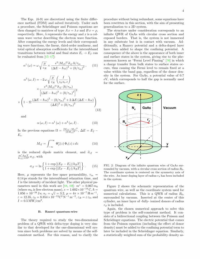
The structure under consideration corresponds to aninfinite QWR of GaAs with circular cross section andexposed borders. That is, the system is not immersedin any substrate but is in contact with vacuum. Ad-ditionally, a Razavy potential and a delta-doped layerhave been added to shape the confining potential. Aconsequence of the above is the appearance of both innerand surface states in the system, giving rise to the phe-nomenon known as “Fermi Level Pinning” [70] in whicha charge transfer from bulk states to surface states oc-curs, thus causing the Fermi level to remain fixed at avalue within the band gap, regardless of the donor den-sity in the system. For GaAs, a potential value of 0.7eV, which corresponds to half the gap is normally usedfor the surface.
x
y
Vacuum
R0rd
z
GaAsNd
FIG. 2: Diagram of the infinite quantum wire of GaAs sur-rounded by vacuum, with a circular cross section of radius R0.The coordinate system is centered on the symmetry axis ofthe wire. An inner doping layer of radius rd has been includedin the system.
Figure 2 shows the schematic representation of thequantum wire, as well as the coordinate system used fornumerical calculations. This is a QWR of radius R0,surrounded by vacuum. Inserted at the center of thiscylinder, an inner layer of -fully- ionized donors of radiusrd is included.
Again, the chosen numerical approach to solve thistype of problem is the self-consistent method. It con-sists of a bidirectional coupling between the Poisson andSchrodinger equations. The electric potential that comesfrom the Poisson equation (including the effect of donordensity) must be added to the confining potential term tolater be included in the Schrodinger equation. Similarly,a statistically weighted sum of the probability density as-

5
sociated with the electronic occupation of the states ofthe Schrodinger problem contributes to the space chargedensity that enters the Poisson equation. This processimplies an iteration scheme where the confining poten-tial becomes modified by the redistribution of charges.
As a starting point of the self-consistent method, andfollowing the Luscombe and Luban procedure [71], weshal consider that electrons in the cross section of theQWR behave as a two-dimensional charge-carrier gas.This indicates that a good approximation for the electrondensity would be the Thomas-Fermi one (Eq. 16). Suchelectron density must contribute to the charge density inthe system and therefore to the Hartree potential that isobtained through the Poisson equation,
n(x, y, T ) = NC F1/2 (β (EF −Υ(x, y, T ))) (16)
where β = 1/kBT is the Boltzmann factor, NC =(2m∗/πβ~2)3/2/4 is the effective density of states,Υ(x, y, T ) is the electronic potential generated by theFermi level pinning on the exposed lateral surface, thelevel of doping and the lateral dimensions of the sys-tem and is given by Υ(x, y, T ) = −e φ(x, y, T ), whereφ(x, y, T ) is the Hartree potential. Besides, e is thecharge of the electron, m∗ is the effective mass, andF1/2(x) is the well known Fermi-Dirac integral. Withthe electron density given by Eq. 16 and the density ofdonors Nd given by Nd for r ≤ rd and 0 for r > rd, it ispossible to write the expression for the charge density inthe system as,
ρ(x, y, T ) = e (Nd − n(x, y, T )) (17)
where εr and ε0 are the relative permittivity and vacuumpermittivity respectively. Note that, unlike the QW, nowthe charge density has a two-dimensional dependence, inthe same way the donor density for this case is identifiedas Nd (for the well system it is labeled as nd). This chargedensity must enter the two-dimensional Poisson equation(Eq. 18) to obtain the Hartree potential,
− ε0εr∇2φ(x, y, T ) = ρ(x, y, T ) (18)
This equation should be solved taking into account theboundary conditions imposed by the Fermi level pinning,which for GaAs takes the form φ(Ω) = −(EF +0.7eV)/e,where Ω represents the QWR boundary. The potential,φ(x, y, T ), obtained through Eq. 18 must contribute tothe potential energy term in the Schrodinger equation,
U(x, y, T ) = −e φ(x, y, T ) + Vc(x, y) (19)
where −e φ(x, y, T ) is the contribution that comes fromthe Poisson equation and the redistribution of chargesdue to doping, and Vc(x, y) is the Razavy 2D poten-tial, which has the same form as Eq. 2, changing z for
√x2 + y2. In this case, V0 = 0.228 eV, A = 2, M = 3,
D = 1.57L, and L = 20 nm. On the other hand, theelectrons are assumed to be totally confined within thevolume of the QWR and, therefore, it must be satisfiedthat Ψ(Ω) = 0 in the Schrodinger equation,
− ~2
2m∗∇2Ψik(~r) + U(x, y, T ) Ψik(~r) = Eik Ψik(~r) (20)
Note that in Eq. 21 we have used the approximationof effective mass for electrons in GaAs. In this equationΨ(~r), the wave function of the system, takes the form,
Ψik(~r) = eikz ψi(x, y) (21)
Considering now the Schrodinger equation in the xyplane, with eigenvalue Ei associated with the stateψi(x, y), we have to solve the problem
− ~2
2m∗∇2ψi(x, y) + U(x, y, T )ψi(x, y) = Ei ψi(x, y),
(22)with ψi(Ω) = 0. From here, it is possible to find thefirst set of eigenfunctions and eigenvalues for the system.With this set we can calculate the electron density asso-ciated with the occupation of the internal states in thesystem,
η(x, y, T ) = ξ∑i=1
F−1/2(β (EF − Ei)) |ψi(x, y)|2 (23)
where ξ = 3√
4NC . This equation represents the densityof electron gas at a point (x, y) and temperature T . Fromthe electron density calculated in Eq. 24, a new profilefor the charge density of the system is obtained:
ρnew(x, y, T ) = e(Nd − η(x, y, T )). (24)
Replacing this charge density into Poisson’s equation(18), a new Hartree potential φnew(x, y, T ) is obtainedthat will -again- contribute to the potential energy termin the Schrodinger equation. Then, a new set of eigen-functions and eigenvalues for the system ψnewi , Enewi isobtained. This set will be associated to a new electrondensity profile ηnew relative to the occupation of eachof each state of the system. In this way, the process isrepeated iteratively until the absolute value of the differ-ence between potential terms corresponding to two suc-cessive self-consistent steps is smaller than a certain tol-erance |U−Uold| < 10−6 eV. When this condition is met,the system is said to have reached self-consistency. Notethat the confining potential and the Razavy potential donot change with the iterative process, only the electro-static potential changes due to the redistribution of thecharge carriers.

6
Once self-consistency has been reached, the final setof eigenvalues and eigenfunctions as well as the self-consistent potential found are the correct solutions forthe quantum wire with exposed boundaries, Razavy po-tential, and donor density Nd. Figure 3 shows the plotsof first five QWR confined state wave functions for threedifferent values of rd; from left to right, each column cor-responds to: rd = 5 nm, rd = 10 nm, and rd = 15 nm.Despite varying the inner radius rd, all the figures main-tain the same cross-sectional area since the outer radiusR0 = 50 nm remains fixed. The electron density Nd hasbeen fixed as 3 × 1019 cm−3 for all three cases, and thetemperature has also been kept at T = 10K. The colorscale in each figure goes from the blue, which correspondsto negative values of the wave function, to dark red whichrepresents positive values. Yellow indicates the points atwhich the wave function is zero. With these parametersa degeneracy between ψ1 and ψ2 appears for all rd. Notehow for rd = 5 nm -first column plots- the state ψ3 hasthe shape of an s-orbital, followed by the state ψ4 whichhas a d-type orbital (in analogy with atomic orbitals).For values of rd = 10 nm and rd = 15 nm, this s stateno longer appears in ψ3, it takes the form of a d state.This means that as long as the value of rd augments, anexchange between states of type s and type d is presentfor the third excited state.
On the other hand, the first row at the top of Fig. 3,corresponds to the ground state ψ0 for each system, againin analogy with the atomic orbitals, a clear symmetryequivalent to an s-type state is evidenced. For all systemconfigurations, it is readily apparent that there is a highprobability of finding the electrons close to the center ofgravity of the structure. Moreover, as rd increases, theprobability at the center of the structure diminishes, atthe time that increases along the radial direction. Then,the electrons tend to be distributed along the cross sec-tion with the increase of the doping region width. Thefirst and second excited states, ψ1 and ψ2, are presentedon the second and third rows from top to bottom. Notethat these states present a symmetry similar to the p-typeorbitals.
FIG. 3: First five wave functions for a confined electron inGaAs quantum wires. The rows from top to bottom are theground state and first four excited states, columns from left toright correspond to rd = 5 nm, rd = 10 nm, and rd = 15 nm,respectively. For all figures the radius of the quantum wire hasbeen set at R0 = 50 nm, T = 10K, and Nd = 3× 1019 cm−3.
III. RESULTS AND DISCUSSION
A. Results Quantum Well
In Fig. 4, we present our results for the confining po-tential, energy levels, Fermi level, and probability den-sities for the lowest four bound electron states in GaAsRazavy-like QWs, considering four different cases of theexternal electric and magnetic fields, as well as dopingconcentration. Despite the inclusion of the third excitedstate, it does not contribute to the electron density sinceit is above the Fermi level of the system. From Fig. 4(a),where these three parameters are set to zero, it is ob-served that the central barrier is high enough such thatthe ground state is almost-degenerate; corresponding tothe ground state -with even symmetry- and the first ex-cited state -with energy very close to the ground stateone- showing odd symmetry with respect to the z = 0point. The energy difference between the ground stateand the second excited state is approximately 150 meV.Notice that the second excited state is located above thecentral barrier. In Fig. 4(b), where an on-center dopingconcentration of nd = 4.5 × 1019 cm−3 is considered inthe absence of external fields (doping of this order is dis-cussed in Ref. [72]), one may observe the appearance ofan additional central potential well. The energy minimaof the two side QWs, which in Fig. 4(a) have zero value,now show a slight shift towards lower energies. Besides,the minimum of the central well positions itself at an en-ergy slightly higher than the energy of the two lateralminima.

7
-10 -5 0 5 10-0.1
0.0
0.1
0.2
0.3
0.4
0.5
-10 -5 0 5 10-0.1
0.0
0.1
0.2
0.3
0.4
0.5
-10 -5 0 5 10-0.1
0.0
0.1
0.2
0.3
0.4
0.5
-10 -5 0 5 10-0.1
0.0
0.1
0.2
0.3
0.4
0.5
(b) nd = 4.5 x 1019 cm-3
F = 0 B = 0
ener
gy (e
V)
(a) nd = 0 F = 0 B = 0
ground state 1st excited state 2st excited state 3st excited state Fermi Level confining potential
(c) nd = 4.5 x 1019 cm-3
F = 30 kV/cm B = 0
ener
gy (e
V)
z (nm)
(d) nd = 4.5 x 1019 cm-3
F = 0 B = 30 T
z (nm)
FIG. 4: (color online) Confining potentials, energy lev-els, Fermi level, and probability density for the lowest fourbounded electron states in a GaAs Razavy-like quantumwells. Four different cases of the external fields and dop-ing concentration (F,B, nd) are considered: (0, 0, 0) (a),(0, 0, 4.5× 1019 cm−3) (b), (30 kV/cm, 0, 4.5× 1019 cm−3) (c),and (0, 30 T, 4.5× 1019 cm−3) (d). In (b-d) the Fermi level isdepicted with the horizontal line close to 200 meV.
Under these conditions, the GaAs Razavy-like doublequantum well in the presence of central doping is trans-formed into a triple quantum well with outer barriersthat rapidly diverge, generating an infinite confining po-tential. The presence of the central well in Fig. 4(b)has the function of coupling the two quantum wells ini-tially observed in Fig. 4(a). In this sense, the break-down of the ground state degeneration is clearly noticed.It is also observed that the first excited state shows ablue shift of 36 meV concerning the ground state. Thelatter, whose energy is 3 meV less than the maximumof the finite potential barriers, is an even function withits maximum probability density in the central region;the presence of shoulders associated with the irregular-ity of the potential well bottom is also well apparent.Besides, the first excited state is an odd function whosemaximum probability density is located in the region ofthe two lateral quantum wells. The second excited state
is remarkably insensitive to the shape of the potentialwell. This is concluded by observing that the two lateralmaximums in the probability density present magnitudesslightly lower than that shown by the central maximum.On the other hand, in Fig. 4(c), where a delta-like dop-ing volume density of nd = 4.5× 1019 cm−3 is combinedwith an applied electric field of 30 kV/cm (developmentsin high electric fields can be seen in Ref. [73, 74]), it ispossibel to see that, by breaking the symmetry of thesystem, the ground state is pushed towards the left-handside well structure while, due to orthogonality conditions,the first excited state displaces its maximum towards theright-side of the system. The ground state has a quasi-constant probability density in the region −5 nm< z < 0.The comparison between the second excited state in Figs.4(b) and 4(c) shows a slight blue shift due to the field-effect without significant changes in the probability den-sity shape. This effect is associated with the fact thatthe electric potential is zero at z = −10 nm. Now, turn-ing to analyzing Fig. 4(d), where a delta-like doping ofnd = 4.5×1019 cm−3 combines with an applied magneticfield of 30 T (some experimental and theoretical worksin high magnetic fields [75–77]), a parabolic confinementappears associated with the second term in the squaredparenthesis of Eq. (5). By comparing the confinementpotentials in Figs. 4(b) and 4(d), it is observed that,as a first effect, the parabolic potential is responsible forequalizing in energy the bottom of the three quantumwells. In this way, the central maximum of the groundstate probability density is reinforced. Additionally, thethree confined states show a blue shift related with thereinforcement of carrier space confinement; noting an in-crease in the separation in energy between the groundstate and the first excited state. The probability densityof the second excited state now appears with three max-ima, all of them with equal amplitude, reflecting a sys-tematic disappearance of the influence of potential wellbottom shape. In Figs. 4(b-d), where central doping ispresent, it is clearly seen that in the three cases there areonly three confined levels with energies lower than theFermi level.
0 50 100 150 2000.00
0.04
0.08
0.12
0.16
B = 0nd = 4.5 x1019 cm-3
ener
gy (e
V)
electric field (kV/cm)
E2 - E1
E3 - E1
E3 - E2
(a)

8
0 5 10 15 20 25 300.03
0.06
0.09
0.12(b)
ener
gy (e
V)
magnetic field (T)
E2 - E1
E3 - E1
E3 - E2
F = 0nd = 4.5 x1019 cm-3
FIG. 5: (color online) Variation of the lowest three energyseparations in a central doped GaAs Razavy-like quantumwell as a function of the applied electric (a) and magnetic (b)field. Calculations are for nd = 4.5× 1019 cm−3.
In Fig. 5, we present the results for the variation ofthe lowest three energy separations (E2 − E1, E3 − E1,and E3 − E2) in a central doped GaAs Razavy-like QWas a function of the applied electric field, without mag-netic field effects, Fig. 5(a), and as a function of theapplied magnetic field, without electric field effects, Fig.5(b). The simulations include a fixed delta-like dopingconcentration, nd = 4.5×1019 cm−3. The results in Figs.5(a) and 5(b) are in complete agreement with those pre-sented in Figs. 4(c) and 4(d), respectively. The electricfield -variable in Fig. 5(a)- has the function of tilting thepotential well profile, generating a greater localization ofthe carriers towards the z < 0 region. This effect trans-lates into greater confinement of the carriers, thereby in-creasing the separation between the confined levels andconsequently the transition energies. The quasi-parallelbehavior of the E2 − E1 and E3 − E1 curves justifiesthe quasi-constant behavior with the electric field of theE3−E2 curve which, in the whole range of electric fieldsconsidered, only presents a variation of 8 meV; less than10%. It is important to note that the wave functions as-sociated to the three states in Fig. 5(a) lose their odd oreven symmetry with respect to the z = 0 point, whichmeans that all inter-subband transitions are allowed. Ascommented, the magnetic field -the variable in Fig. 5(b)-is responsible for a parabolic potential whose effect is toincrease the localization of all confined states within theregion close to z = 0. This greater localization of thestates translates into an increase in the transition ener-gies with the applied magnetic field. Due to its greaterextension in space, the second excited state (Φ3) is theone most susceptible to being spatially modified by theeffect of the applied magnetic field. The ground state(Φ1), which has its maximum probability density closeto the z = 0 region, is essentially insensitive to the ef-fects of the magnetic field. Combining these two aspects,one may understand why, as in Fig. 5(a), the E2−E1 andE3 −E1 transition energies are the most sensitive to the
magnetic field, with a growing behavior and parallel toeach other. This justifies that in the range of magneticfields, the E3 − E2 transition energy is constant. Thewave functions associated with the three states consid-ered in the transitions of Fig. 5(b) preserve their even orodd symmetries. The Φ1 and Φ3 states are even functionsconcerning z = 0 while the Φ1 state is an odd function.Consequently, only the 1 → 2 and 2 → 3 transitions areallowed whereas the 1→ 3 transition is forbidden.
0 50 100 150 2000.0
0.3
0.6
0.9
1.2
1.5
0 50 100 150 2001
2
3
4
5
6
0 50 100 150 2000
50
100
150
200
250
300
mat
rix e
lem
ents
(10-3
nm
2 )
M122
M132
M232
(a) (b)
occu
panc
y ra
tio -
if
12
13
23
if Mif2 (E
f - E
i) (m
eV n
m2 )
electric field (kV/cm)
12 M122 (E2 - E1)
13 M132 (E3 - E1)
23 M232 (E3 - E2)
(c)
FIG. 6: (color online) Variation of the reduced dipole ma-trix elements-|Mif |2 (a), the occupancy ratio-σif (b), and thefunction Fif = σif |Mif |2 (Ef − Ei) (c) in a central dopedGaAs Razavy-like quantum well as a function of the appliedelectric field, for zero magnetic field. The results are fornd = 4.5× 1019 cm−3.
9
0 10 20 301.0
1.1
1.2
1.3
1.4
1.5
0 10 20 301.50
2.50
3.50
4.50
0 10 20 3050
100
150
200
250
300
(a)m
atrix
ele
men
ts (1
0-3 n
m2 )
M122
M232
occu
panc
y ra
tio -
if
12
13
23
(b)
if M
if2 (Ef -
Ei)
(meV
nm
2 )
magnetic field (T)
12 M122 (E2 - E1)
23 M232 (E3 - E2)
(c)
FIG. 7: (color online) Variation of the reduced dipole ma-trix elements-|Mif |2 (a), the occupancy ratio-σif (b), and thefunction Fif = σif |Mif |2 (Ef − Ei) (c) in a central dopedGaAs Razavy-like quantum well as a function of the ap-plied magnetic field for zero electric field. The results arefor nd = 4.5× 1019 cm−3.
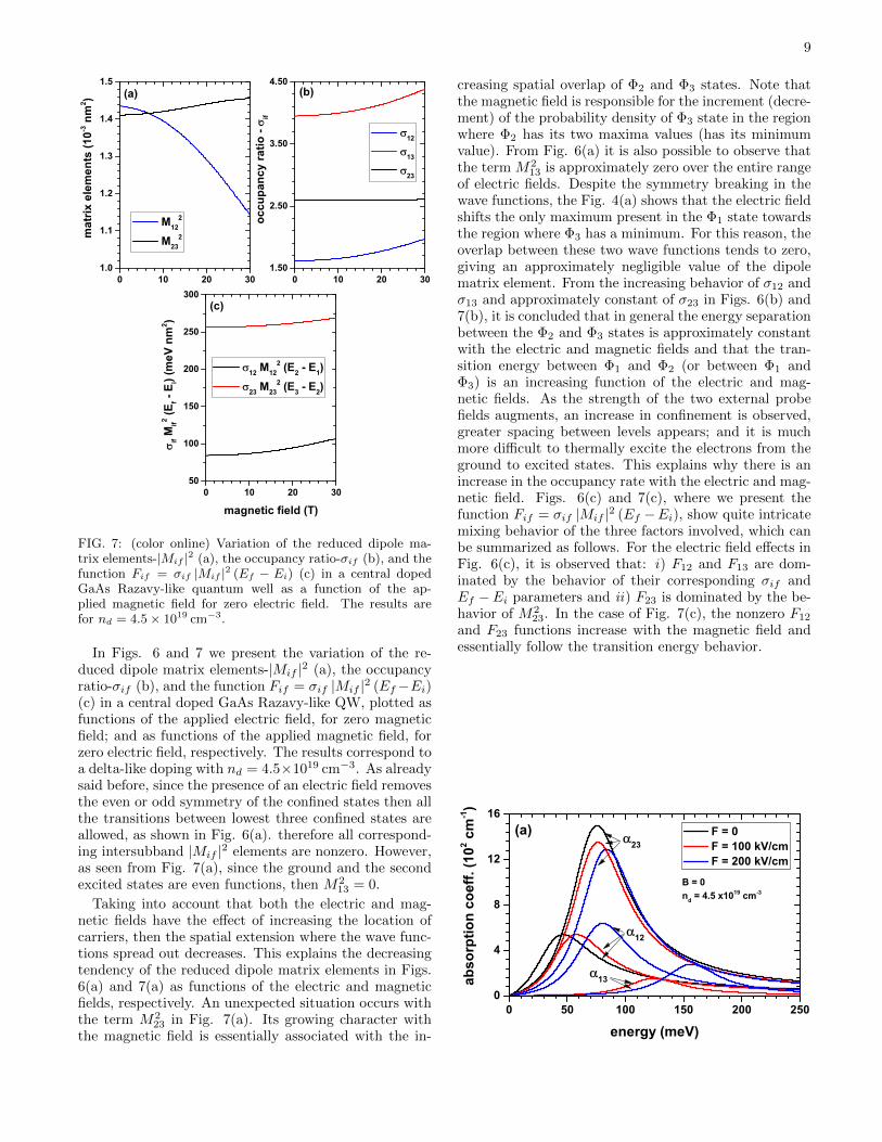
In Figs. 6 and 7 we present the variation of the re-duced dipole matrix elements-|Mif |2 (a), the occupancyratio-σif (b), and the function Fif = σif |Mif |2 (Ef−Ei)(c) in a central doped GaAs Razavy-like QW, plotted asfunctions of the applied electric field, for zero magneticfield; and as functions of the applied magnetic field, forzero electric field, respectively. The results correspond toa delta-like doping with nd = 4.5×1019 cm−3. As alreadysaid before, since the presence of an electric field removesthe even or odd symmetry of the confined states then allthe transitions between lowest three confined states areallowed, as shown in Fig. 6(a). therefore all correspond-ing intersubband |Mif |2 elements are nonzero. However,as seen from Fig. 7(a), since the ground and the secondexcited states are even functions, then M2
13 = 0.
Taking into account that both the electric and mag-netic fields have the effect of increasing the location ofcarriers, then the spatial extension where the wave func-tions spread out decreases. This explains the decreasingtendency of the reduced dipole matrix elements in Figs.6(a) and 7(a) as functions of the electric and magneticfields, respectively. An unexpected situation occurs withthe term M2
23 in Fig. 7(a). Its growing character withthe magnetic field is essentially associated with the in-
creasing spatial overlap of Φ2 and Φ3 states. Note thatthe magnetic field is responsible for the increment (decre-ment) of the probability density of Φ3 state in the regionwhere Φ2 has its two maxima values (has its minimumvalue). From Fig. 6(a) it is also possible to observe thatthe term M2
13 is approximately zero over the entire rangeof electric fields. Despite the symmetry breaking in thewave functions, the Fig. 4(a) shows that the electric fieldshifts the only maximum present in the Φ1 state towardsthe region where Φ3 has a minimum. For this reason, theoverlap between these two wave functions tends to zero,giving an approximately negligible value of the dipolematrix element. From the increasing behavior of σ12 andσ13 and approximately constant of σ23 in Figs. 6(b) and7(b), it is concluded that in general the energy separationbetween the Φ2 and Φ3 states is approximately constantwith the electric and magnetic fields and that the tran-sition energy between Φ1 and Φ2 (or between Φ1 andΦ3) is an increasing function of the electric and mag-netic fields. As the strength of the two external probefields augments, an increase in confinement is observed,greater spacing between levels appears; and it is muchmore difficult to thermally excite the electrons from theground to excited states. This explains why there is anincrease in the occupancy rate with the electric and mag-netic field. Figs. 6(c) and 7(c), where we present thefunction Fif = σif |Mif |2 (Ef −Ei), show quite intricatemixing behavior of the three factors involved, which canbe summarized as follows. For the electric field effects inFig. 6(c), it is observed that: i) F12 and F13 are dom-inated by the behavior of their corresponding σif andEf −Ei parameters and ii) F23 is dominated by the be-havior of M2
23. In the case of Fig. 7(c), the nonzero F12
and F23 functions increase with the magnetic field andessentially follow the transition energy behavior.
0 50 100 150 200 2500
4
8
12
16
B = 0nd = 4.5 x1019 cm-3
13abso
rptio
n co
eff.
(102 c
m-1)
energy (meV)
F = 0 F = 100 kV/cm F = 200 kV/cm
23
12
(a)

10
0 50 100 150 200 2500
5
10
15
20(b)
F = 0nd = 4.5 x1019 cm-3
12
abso
rptio
n co
effic
. (10
2 cm
-1)
energy (meV)
B = 0 B = 15 T B = 30 T
23
FIG. 8: (color online) Variation of the total optical absorptioncoefficient in a central doped GaAs Razavy-like quantum wellas a function of the z-polarized incident photon energy forthree different values of the applied electric field, for zeromagnetic field (a) and for three values of the applied magnetic,for zero electric field (b). The results are for nd = 4.5 ×1019 cm−3.
In Fig. 8 we present the variation of the total opti-cal absorption coefficient in a central δ-like doped GaAsRazavy-like QW as a function of the z-polarized inci-dent photon energy for three different values of the ap-plied electric field, with B = 0 (a) and for three valuesof the applied magnetic, with F = 0 (b) and keepingconstant the nd concentration. According to Eq. (11),the magnitude of the first-order correction resonant peakof the optical absorption coefficient is proportional toFif = |M2
if σif (Ef − Ei) which is precisely the quantity
reported in Figs. 6(c) and 6(c). The incident radiationintensity chosen in this study is I = 0.5 MW/cm2 and,under such assumption, a clear dominance of the linearcontribution to the total light absorption is present. Notethat the magnitude of the maxima of αij in all the curvesof Fig. 8 follow the behavior of Fij reported in Figs. 6and 7. For example, in Fig. 6(c), we can see that F23
decreases with the electric field, a situation that is iden-tical to the decrease of the resonant peak of α23 in thethree corresponding curves in Fig. 8(a) as it increases theelectric field. The almost constant behavior of the mag-nitude of the resonant peak of α23 in Fig. 8(b) is directlyrelated to the slight variation shown by F23 in Fig. 7(c).The absence of the α13 coefficient in Fig. 8(b) for allthe magnetic fields strengths considered and in Fig. 8(a)for F = 0 is since the α13 transitions are forbidden be-tween states that have the same even symmetry. As men-tioned, in general, the electric and magnetic fields usedas external probes in this study are responsible for theincrease in carriers’ confinement, which finally translatesinto a greater spacing between adjacent levels and con-sequently in an increase in the transition energies. Thisfact is in perfect coherence with the blue shift shown bythe resonant peaks of the total absorption coefficient asthe electric field increases, as shown in Fig. 8(a), or as
the magnetic field increases, as shown in Fig. 8(b).
0.9 1.0 1.1 1.2 1.3 1.4 1.50.02
0.04
0.06
0.08
0.10
0.12
0.140.9 1.0 1.1 1.2 1.3 1.4 1.5
0.6
0.9
1.2
1.5
1.8
0.9 1.0 1.1 1.2 1.3 1.4 1.51
2
3
4
5
0.9 1.0 1.1 1.2 1.3 1.4 1.550
100
150
200
250
300
Nd (1017nm-2)
ener
gy (e
V) (E2 - E1) (E3 - E1) (E3 - E2)
(c)
mat
rix e
lem
ents
(10-3
nm
2 )
M122
M232
(a)
occu
panc
y ra
tion
- if
12
13
23
(b)
(d)
if Mif2 (E
f - E
i) (m
eV n
m2 )
Nd (1017 m-2)
12 M122 (E2 - E1)
23 M232 (E3 - E2)
FIG. 9: (color online) Variation of the reduced dipole ma-trix elements-|Mif |2 (a), the occupancy ratio-σif (b), thetransition energies-Ef − Ei (c), and the function Fif =σif |Mif |2 (Ef −Ei) (d) in a central doped GaAs Razavy-likequantum well as a function of the nd-doping concentration.The results are for F = 0 and B = 0.
In Fig. 9 we present the variation of the reduced dipolematrix elements (a), the occupancy ratio (b), the tran-sition energies (c), and the Fif -function (d) in a centralδ-like doped GaAs Razavy-like QW as a function of thedoping volume concentration for zero electric and mag-netic field. As shown in Fig. 4(b), central doping cre-ates a potential well in the center of the structure, givingrise to a system of three coupled wells in the Razavy-like double quantum well system studied here. Whennd = 4.5×1019 cm−3, see Fig. 4(b), it is observed that thecentral well, where doping exists, has its minimum withenergy slightly higher than the original two minimumsof the Razavy-like double quantum well. As nd growsfrom that value, the two potential barriers that separatethe wells decrease in their heights until they finally col-lapse, and the system evolves from three potential wellsto a single QW that drags the ground state successivelytowards lower energies. This effect is responsible for theincreasing behavior of the E2−E1 and E3−E1 transitionenergies in Fig. 9(c). The central potential well, with in-creasing nd, confines within it the Φ1 and Φ2 states, withwhich an increasing behavior appears reinforced by the
11
confinement of the E2 − E1 transition energy. This factjustifies that the slope with nd of the E2 −E1 transitionis higher than that exhibited by E3−E1, which explainsthe decreasing character of the E3 − E2 transition. Asthe Φ1 and Φ2 states are confined in the central well, agreater localization oaround z = 0 gives rise to the di-minishing character of M2
12 in Fig. 9(a). Due to theincrement in the localization of Φ2 close to z = 0 andthat the spatial extension of Φ3 shows negligible changeswith the increase of nd, the augmenting character of M2
23
is justified. The variations of σif in Fig. 9(b) exactlyfollow the behavior of Ef − Ei as previously justified.Fig. 9(d) shows unequivocally that in the Fif function,the dominant factors are the transition energies and theoccupancy ratio.
0 50 100 150 200 2500
3
6
9
12
15
12abso
rptio
n co
eff.
(102 c
m-1)
energy (meV)
nd = 4.5 x 1019 cm-3
nd = 6.0 x 1019 cm-3
nd = 7.5 x 1019 cm-3
F = 0B = 0 23
FIG. 10: (color online) Variation of the total optical absorp-tion coefficient α12 and α23 in a central doped GaAs Razavy-like quantum well as a function of the incident photon energyfor three different values of the nd-doping concentration. Theresults are for F = 0 and B = 0.
Figure 10 contains our results for the variation of thetotal optical absorption coefficient α12 and α23 in the in-vestigated GaAs Razavy-like QW with on-center delta-like doping, plotted as a function of the incident photonenergy for three different values of the nd-doping concen-tration in the absence of any external field. The absenceof the α13 transitions is justified by the symmetric natureof the structure, in which case both the ground state andthe second excited state are even functions between whichthe dipole matrix element is zero. The red/blue shift ofα12/α23 is explained by the results in Fig. 9(c). Like-wise, Fig. 9(d) justifies the variations in the magnitudesof the resonant structures and again makes it possible toargue that the first order correction is the dominant onein the optical absorption coefficient.
B. Results Quantum Wire
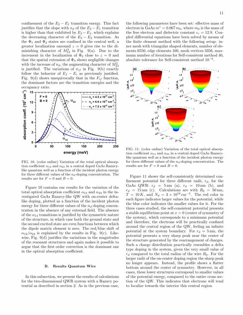
In this subsection, we present the results of calculationsfor the two-dimensional QWR system with a Razavy po-tential as described in section 2. As in the previous case,
the following parameters have been set: effective mass ofelectron in GaAs m∗ = 0.067m0, where m0 is the mass ofthe free electron and dielectric constant εr = 12.9. Cou-pled differential equations have been solved by means ofthe finite element method with the following setup: in-ner mesh with triangular shaped elements, number of ele-ments 6550, edge elements 160, mesh vertices 3356, max-imum number of iterations for Self-consistent method 40,absolute tolerance for Self-consistent method 10−6.
FIG. 11: (color online) Variation of the total optical absorp-tion coefficient α12 and α23 in a central doped GaAs Razavy-like quantum well as a function of the incident photon energyfor three different values of the nd-doping concentration. Theresults are for F = 0 and B = 0.
Figure 11 shows the self-consistently determined con-finement potential for three different radii, rd, for theGaAs QWR: rd = 5 nm (a), rd = 10 nm (b), andrd = 15 nm (c). Calculations are with R0 = 50 nm,T = 10K, and Nd = 3 × 1019 cm−3. The red color ineach figure indicates larger values for the potential, whilethe blue color indicates the smaller values for it. For thethree cases studied, the self-consistent potential presentsa stable equilibrium point at x = 0 (center of symmetry ofthe system), which corresponds to a minimum potentialand therefore, the electrons will be practically confinedaround the central region of the QW, feeling an infinitepotential at the system boundary. For rd = 5 nm, thepotential presents a very sharp peak near the center ofthe structure generated by the rearrangement of charges.Such a charge distribution practically resembles a deltatype doping in the system, given the very small value ofrd compared to the total radius of the wire R0. For thelarger radii of the on-center doping region the sharp peakno longer appears. Instead, the profile shows a flatterbottom around the center of symmetry. However, in allcases, these lower structures correspond to smaller valuesof the potential energy, compared to the entire cross sec-tion of the QW. This indicates that electrons will tendto localize towards the interior this central region.
12
ener
gy (e
V)
x (nm)
Razavy rd = 5 nm rd = 10 nm rd = 15 nm
(a) (b)
(x,10K
)/Nd
x (nm)
rd = 5 nm rd = 10 nm rd = 15 nm
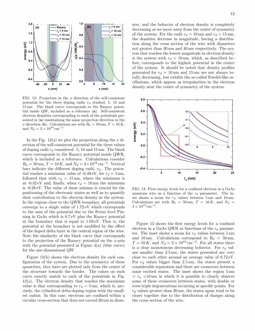
FIG. 12: Projection in the x direction of the self-consistentpotential for the three doping radio rd studied, 5, 10 and15 nm. The black curve corresponds to the Razavy poten-tial inside QW, included as a reference (a). Self-consistentelectron densities corresponding to each of the potentials pre-sented in (a) maintaining the same projection direction in thex direction (b). Calculations are with R0 = 50 nm, T = 10K,and Nd = 3× 1019 cm−3.
In the Fig. 12(a) we plot the projection along the x di-rection of the self-consistent potential for the three valuesof doping radii rd considered: 5, 10 and 15 nm. The blackcurve corresponds to the Razavy potential inside QWR,which is included as a reference. Calculations considerR0 = 50 nm, T = 10K, and Nd = 3×1019 cm−3. Verticalbars indicate the different doping radii, rd. The poten-tial reaches a minimum value of -0.49 eV, for rd = 5 nm,followed that with rd = 15 nm, where the minimum isat -0.32 eV and, finally, when rd = 10 nm the minimumis -0.28 eV. The value of these minima is crucial for thepositioning of the electronic states as well as to quantifytheir contribution to the electron density in the system.In the regions close to the QWR boundary, all potentialsconverge to a single value of 1.72 eV which correspondsto the sum of the potential due to the Fermi level Pin-ning in GaAs which is 0.7 eV plus the Razavy potentialat the boundary that is equal to 1.02 eV. That is, thepotential at the boundary is not modified by the effectof the doped delta layer in the central region of the wire.Note the similarity of the black curve that correspondsto the projection of the Razavy potential on the x-axiswith the potential presented in Figure 4(a) (blue curve)for the one-dimensional QW.
Figure 12(b) shows the electron density for each con-figuration of the system. Due to the symmetry of thesequantities, they have are plotted only from the center ofthe structure towards the border. The colors on eachcurve exactly match to each of the potentials in Fig.12(a). The electron density that reaches the maximumvalue is that corresponding to rd = 5 nm, which is, pre-cisely, the cylindrical delta-doping region with the small-est radius. In this case, electrons are confined within acircular cross-section that does not exceed 20 nm in diam-
eter, and the behavior of electron density is completelydecreasing as we move away from the center of symmetryof the system. For the radii rd = 10 nm and rd = 15 nm,the densities decrease in magnitude, having a distribu-tion along the cross section of the wire with diametersnot greater than 30 nm and 40 nm respectively. The sys-tem that reaches the lowest magnitude in electron densityis the system with rd = 10 nm, which, as described be-fore, corresponds to the highest potential in the centerof the system. It should be noted that density profilesgenerated for rd = 10 nm and 15 nm are not always to-tally decreasing, but exhibit the so-called Friedel-like os-cillations, which appear as irregularities in the electrondensity near the center of symmetry of the system.
5 10 15 20 25-0.4
-0.2
0.0
0.2
0.4
0.6
0.8
6 8 10-0.2
-0.1
0.0
0.1
0.2
ener
gy (e
V)
rd (nm)
FIG. 13: First energy levels for a confined electron in a GaAsquantum wire as a function of the rd parameter. The in-set shows a zoom for rd values between 5 nm and 10 nm.Calculations are with R0 = 50 nm, T = 10K, and Nd =3× 1019 cm−3.
Figure 13 shows the first energy levels for a confinedelectron in a GaAs QWR as functions of the rd parame-ter. The inset shows a zoom for rd values between 5 nmand 10 nm. Calculations correspond to R0 = 50 nm,T = 10K, and Nd = 3× 1019 cm−3. For all states thereis a clear monotonous decreasing behavior. For rd val-ues smaller than 2.5 nm, the states presented are veryclose to each other around an average value of 0.72 eV.For rd values bigger than 2.5 nm, the states present aconsiderable separation and there are crossovers betweensome excited states. The inset shows the region 5 nm< rd <10 nm in which it is possible to clearly observesome of these crossovers between states, with double oreven triple degenerations occurring at specific points. Forrd values greater than 20 nm, the states again tend to becloser together due to the distribution of charges alongthe cross section of the wire.

13
5 10 15 20 25 30
0.68
0.70
0.72
0.74en
ergy
(eV)
Nd (1018 cm-3)
FIG. 14: First energy levels for a confined electron in a GaAsquantum wire as a function of the Nd parameter. Calculationsare with R0 = 50 nm, rd = 2 nm, and T = 10K.
The plot in Figure 14 shows the lowest energy levels fora confined electron in a GaAs QWR as a function of theNd parameter. Results presented are for R0 = 50 nm,rd = 2 nm, and T = 10K. With this setup, all statespresent a parallel and approximately linear behavior, ex-isting degeneration of order two for all the states exceptfor the ground one. It should be noted that, unlike Fig.13 in which the rd is varied, there are no longer anycrossovers between the states. Note that the first excitedstate and the ground state present very close energies,with a separation of approximately 0.7 meV, whilst theother excited states exhibit a more notable separation.
0 2 4 6 8 100.0
0.2
0.4
0.6
0.8
1.0
(x,10K
)/Nd
x (nm)
(a)rd = 5 nm
0 3 6 9 12 150.0
0.1
0.2
0.3
0.4
rd = 10 nm
(x,10K
)/Nd
x (nm)
(b)
0 4 8 12 16 200.0
0.1
0.2
0.3
0.4
0.5
rd = 15 nm
(x,10K
)/Nd
x (nm)
(c)
FIG. 15: Electron density and |ψi(x, y = 0)|2 that contributewith the highest percentage to the density profile at the pointsmarked with the dashed lines. Results are for rd = 5 nm (a),rd = 10 nm (b), and rd = 15 nm (c) QW. Calculations arewith R0 = 50 nm, T = 10K, and Nd = 3× 1019 cm−3.
The electron density appears in Fig. 15 as a functionof the distance from the QWR center (along the x direc-tion), together with the those quantities, |ψi(x, y = 0)|2,that contribute with the highest percentage to the den-sity profile at the points marked with the dashed lines.Results correspond for rd = 5 nm (a), rd = 10 nm (b),and rd = 15 nm (c) QWR. Calculations were performedwith R0 = 50 nm, T = 10K, and Nd = 3× 1019 cm−3.
In Fig. 15(a) the projection of the electron densityalong the x direction is presented for rd = 5 nm and, forthis configuration, there are no oscillations in the den-sity profile. The dashed line corresponds to the point atwhich the percentage contribution of each of the statesof the system to the total electron density has been cal-culated. This contribution is presented in detail in Table1. For this first system, the electron density profile isdue only to the contribution of four states. the highestcontribution is due to the ground state ψ0 with 73.1%corresponding to the red curve in Fig. 15(a), followedby state ψ3 with 25.1%. No Friedel-like oscillations arepresent in this case. Fig. 15(b) contains the electrondensity profile for rd = 10 nm and the states that presenta contribution greater than 10% at the point x = 2.1 nmmarked with the dashed line. For the total electrondensity, a contribution of eight states is present as re-ported in Table 1. Again, the state that has a greatercontribution is ψ0, with 42.8%, and corresponds to thered curve in the figure. It is followed by the state ψ5
which is already a higher state with 21.2% and later thestate ψ1 with 17.8%. The appearance of this oscillationis mainly due to the occupation of the lowest states inthe system (ψ0 and ψ1) with a contribution greater than60%. Fig. 15(c) presents the electron density profile forrd = 15 nm, together with the probability densities ofstates that present a contribution greater than 9% to theelectron density at the point x = 4.3 nm -marked withthe dashed line. Comparing with figures (a) and (b),in this case the first oscillation appears further from the

14
center of symmetry of the system. It should be notedthat the electron density for this case contains contribu-tions from thirty states, however, none of them exceedsthe 19% contribution to this Friedel-like oscillation as ev-idenced in Table 1. The state that contributes the most(state with the highest occupancy at this specific point)is one of the higher states, ψ8, with 18.5% followed bythe ground state, ψ0, with 15.1%. The Table 1 does notinclude states with a contribution lower than 1%. Com-paring the three values of rd and the data collected inTable 1, it is possible to conclude that as the value ofrd augments, the ground state ceases to be the predom-inant state in terms of occupancy. Instead, a significantcontribution from the highest states in the system willoccur.
Contribution by state (%)rd (nm) ⇒ 5 10 15
ψ0 73.1 42.8 15.1ψ1 0.5 17.8 13.2ψ2 1.3 0.3 1.7ψ3 25.1 1.0 1.6ψ4 0.9 3.0ψ5 21.2 6.0ψ8 12.3 18.5ψ9 3.7 4.2ψ12 9.4ψ13 2.7ψ18 3.3ψ19 7.9ψ20 1.8ψ25 4.8ψ26 3.2ψ27 1.2
TABLE I: Contribution in percentage of each of the states tothe oscillations in the density profile presented in figure 15.
ener
gy (e
V)
x (nm)
(x, 1
0K)/N
d
x (nm)
FIG. 16: Projection of the self-consistent potential in the xdirection considering two different doping zones, the blackcurves correspond to a central cylinder-shaped doping, as in-dicated by the dark vertical column, the red curves correspondto a cylindrical ring-shaped doping such as show the two lightred columns. The dashed lines are for Nd = 1 × 1018 cm−3
and the solid lines are for Nd = 5 × 1018 cm−3. The insetshows the electron density obtained for Nd = 5× 1018 cm−3.Calculations are with R0 = 50 nm, rd = 5 nm, and T = 10K.
Finally, in order to have a comparison about the ef-fect of doping geometry on the self-consistent potentialin the cylindrical Razavy-like QWR, Fig. 16 shows theprojection of the self-consistent potential along the x di-rection considering two different doping zones, the blackcurves correspond to a central cylinder-shaped doping,as indicated by the dark vertical column, the red curvescorrespond to a cylindrical ring-shaped doping (the twolight red columns in the figure indicate the cross sectionof the ring in the xz plane, the columns are centered atx = −30 nm and x = 30 nm respectively). The dashedlines are for Nd = 1 × 1018 cm−3 and the solid lines arefor Nd = 5 × 1018 cm−3. The inset shows the electrondensity obtained for Nd = 5 × 1018 cm−3. Calculationsare with R0 = 50 nm, rd = 5 nm, and T = 10K. Whenthe doping corresponds to the central cylinder, that is, tothe black curves, one observes that when the density ofdonors in the system increases, there is a considerable de-crease of the potential in the central zone. This is muchmore significant when the doping is included in a regionwith the shape of a cylindrical ring (red curves), wherethe potential is lowered by an average of 0.5 eV in the re-gions between -30 nm and 30 nm. It should be noted thatin the latter case there is no longer a specific decrease inthe central area, that is, the repulsive character is notlost in the center of symmetry. Analyzing the continuousblack curve it is possible to realize that, for higher donordensities, the dominant potential in the system will bethe potential due to the redistribution of charges, thatis, the Hartree potential and the Razavy potential losessignificance. Therefore, when the density of donors ac-cumulates in a central cylinder, the self-consistent elec-tron density will be very sensitive to the magnitude ofthese donors since they can drastically modify the po-tential profile. The opposite case occurs when the donordensity accumulates in a cylindrical ring. There, as thedonor density increases, the dominant potential remainsthe Razavy one, and the Hartree potential only gener-ates a decrease in magnitude of the potential withoutdrastically modifying the shape. The inset in Fig. 16shows the electron density for Nd = 5 × 1018 cm−3 forthe system with cylindrical ring doping. By comparingthis result with the one presented in Fig. 12(b), we see atotally different profile in which the electrons accumulatemostly in the area of doped ring and, despite being at alow temperature, no Friedel-like oscillations are present.

15
IV. CONCLUSIONS
By using the effective mass and parabolic band ap-proximations, the finite difference method, as well as aself-consistent calculation, we have investigated the fea-tures of total optical absorption coefficient of confinedelectrons in a delta-like doped Razavy-like quantum wellunder the combined effects of externally applied electricand magnetic field. In the absorption peaks, a clear blueshift is evidenced for all the transitions studied, keep-ing the donor density fixed, the shift being more signifi-cant for changes in the electric field than in the magneticfield, in all cases a change in the magnitude of the opticalabsorption peaks is presented. The transition with thegreatest resistance to modifications due to external fieldsis α23. On the other hand, with the increase in donordensity, red and blue shifts of the absorption peaks werealso reported, as well as a decrease in their magnitudedepending on the transition studied. This allows us totune the system without modifying geometric parame-ters directly, only applying external fields or increasingthe density of donors to obtain the maximum absorptionof the material in the positions that are required for acertain application.
On the other hand, the delta-doping effect on electronstates has been analyzed in quantum wire systems withexposed borders and circular cross-section subjected toan internal Razavy-like potential at low temperatures.Effects of varying geometric parameters such as the widthof delta-doped layer, and not geometric as the density ofdonors in the system have been studied. In both casesa decrease in the magnitude of all electronic states hasbeen found both with the increase of rd and Nd. The ap-pearance of irregularities in the electron density profilehas been reported for rd = 10 nm and 15 nm, these oscil-lations are Friedel-like and have been explained by meansof the occupation of the electronic states of the system.We hope that this research will stimulate future investi-gations related to intentional doping in low-dimensionalsemiconductor heterostructures.
Acknowledgments
CAD is grateful to the Colombian Agencies: CODI-Universidad de Antioquia (Estrategia de Sostenibilidadde la Universidad de Antioquia and projects ”Efectosde capas delta dopadas en pozos cuanticos como fotode-tectores en el infrarrojo”, ”Propiedades magneto-opticasy optica no lineal en superredes de Grafeno”, ”Efec-tos opticos intersubbanda, no lineales de segundo or-den y dispersion Raman, en sistemas asimetricos de po-zos cuanticos acoplados”, and ”Estudio de propiedadesopticas en sistemas semiconductores de dimensionesnanoscopicas”), and Facultad de Ciencias Exactas yNaturales-Universidad de Antioquia (CAD exclusive ded-ication project 2020-2021). CAD also acknowledgesthe financial support from El Patrimonio Autonomo
Fondo Nacional de Financiamiento para la Ciencia, laTecnologıa y la Innovacion Francisco Jose de Caldas(project: CD 111580863338, CT FP80740-173-2019).JAGC acknowledges the financial support from ”Uni-versity of Antioquia Doctoral Scholarship” in December2020, to the doctoral program, and to the postgraduatemanagement of the University of Antioquia. MEMR ac-knowledges Mexican Conacyt for support through GrantA1-S-8218.
Author contributions statementThe contributions of the authors are as follows:
Hassen Dakhlaoui: proposed the problem and wasresponsible of the numerical calculations and writing ofthe manuscript.
J. A. Gil-Corrales: was responsible of the numericalcalculations and writing of the manuscript.
A. L. Morales: participated in the discussion and writingof the manuscript.
E. Kasapoglu: was responsible of the numerical calcula-tions and discussion.
A. Radu: participated in the discussion and writing ofthe manuscript.
R. Restrepo: participated in the discussion and writingof the manuscript.
V. Tulupenko: participated in the discussion and writingof the manuscript.
J. A. Vinasco: was responsible of the numerical calcula-tions.
M. E. Mora-Ramos: participated in the discussion andwriting of the manuscript.
C. A. Duque: was responsible of the numerical calcula-tions, discussion, and writing of the manuscript.
Competing interests statement
The authors do not have any financial and non-financialcompeting interests statement.
16
Data availability statement All the files with tables,figures, and codes are available. The corresponding au-
thor will provide all the files in case they are requested.
[1] R. L. Restrepo, J. P. Gonzalez-Pereira, E. Kasapoglu, A.L. Morales, and C. A. Duque, Linear and nonlinear op-tical properties in the terahertz regime for multiple-stepquantum wells under intense laser field: electric and mag-netic field effects, Opt. Mater. 86, 590–599 (2018).
[2] E. C. Niculescu, Electromagnetically induced trans-parency in an asymmetric double quantum well un-der non-resonant, intense laser fields, Opt. Mater. 64,540–547 (2017).
[3] H. V. Phuc, N. Duy Anh Tuan, and L. Dinh, Linear andnonlinear magneto-optical absorption in a quantum wellmodulated by intense laser field, Superlattice Microst.100, 1112–1119 (2016).
[4] J.-F. You, Q. Zhao, Z.-H. Zhang, J.-H. Yuan, K.-X. Guo,and E. Feddi, The effect of temperature, hydrostatic pres-sure and magnetic field on the nonlinear optical proper-ties of AlGaAs/GaAs semi-parabolic quantum well, Int.J. Mod. Phys. B 33, 1950325 (12pp) (2019).
[5] G. Liu, R. Liu, G. Chen, Z. Zhang, K. Guo, and L. Lu,Nonlinear optical rectification and electronic structure inasymmetric coupled quantum wires, Results Phys. 17,103027 (6pp) (2020).
[6] G. Liu, K. Guo, L. Xie, Z. Zhang, and L. Lu, Tun-ability of linear and nonlinear optical absorption inlaterally-coupled AlxGa1−xAs/GaAs quantum wires, J.Alloy. Compd. 746, 653–659 (2018).
[7] M. J. Karimi and M. Hosseini, Electric and magneticfield effects on the optical absorption of elliptical quan-tum wire, Superlattice Microst. 111, 96–102 (2017).
[8] E. Kasapoglu, C. A. Duque, M. E. Mora-Ramos,and I. Sokmen, The effects of the intense laser fieldon the nonlinear optical properties of a cylindricalGa1−xAlxAs/GaAs quantum dot under applied electricfield, Physica B 474, 15–20 (2015).
[9] M. G. Barseghyan, H. M. Baghramyan, A. A. Ki-rakosyan, and D. Laroze, The transition from double tosingle quantum dot induced by THz laser field, Physica E116, 113758 (4pp) (2020).
[10] A. Ghosh, A. Bera, and M. Ghosh, Modulating bindingenergy and interband emission energy of impurity dopedquantum dots in presence of Gaussian white noise, Curr.Smart Mater. 2, 56–64 (2017).
[11] I. Karabulut and E. Paspalakis, The role of perma-nent dipoles on the intensity-dependent nonlinear opticalproperties in asymmetric coupled quantum wells under astatic electric field, Physica E 81, 294–301 (2016).
[12] K. Li, K. Guo, X. Jiang, and M. Hu, Effect of position-dependent effective mass on nonlinear optical propertiesin a quantum well, Optik 132, 375–381 (2017).
[13] B. T. Diroll, M. Chen, I. Coropceanu, K. R. Williams,D. V. Talapin, P. Guyot-Sionnest, and R. D. Schaller,Polarized near-infrared intersubband absorptions in CdSecolloidal quantum wells, Nat. Commun. 10, 4511 (9pp)(2019).
[14] H. Dakhlaoui and M. Nefzi, Simultaneous effect of impu-rities, hydrostatic pressure, and applied potential on theoptical absorptions in a GaAs field-effect transistor, Re-
sults Phys. 15, 102618 (7pp) (2019).[15] H. Noverola-Gamas, L. M. Gaggero-Sager, and O.
Oubram, Interlayer distance effects on absorption coef-ficient and refraction index change in p-type double-δ-doped GaAs quantum wells, Chinese Phys. B 28, 124207(5pp) (2019).
[16] Q. Zhao, S. Aqiqi, J.-F. You, M. Kria, K.-X. Guo,E. Feddi, Z.-H. Zhang, and J.-H. Yuan, Influence ofposition-dependent effective mass on the nonlinear op-tical properties in AlxGa1−xAs/GaAs single and doubletriangular quantum wells, Physica E 115, 113707 (7pp)(2020).
[17] Ri. Betancourt-Riera, Re. Betancourt-Riera, L. A.Ferrer-Moreno, and A. D. Sanu-Ginerte, Electron statesand electron Raman scattering in a semiconductor quan-tum well with step-barriers: electric field effect, PhysicaB 575, 411700 (7pp) (2019).
[18] B. Amiri and A. Belghachi, First principles investigationof absorption coefficient in quantum well designed for so-lar cells, Optik 202, 163554 (6pp) (2020).
[19] H. Yildirim, Many-body effects on intersubband tran-sitions in polar ZnO/ZnMgO multiple quantum wells,Physica B 571, 26–31 (2019).
[20] Y.-Y. Chen, Y.-N. Li, R.-G. Wan, and H.-W. Yan, Tun-able double-beam optical bistability in an asymmetric dou-ble quantum-well system, Phys. Lett. A 383, 125921(7pp) (2019).
[21] S. Panda, T. Das, and B. K. Panda, Nonlinear opti-cal susceptibilities in InxGa1−xN/GaN hexagonal singlequantum well under applied electric field, SuperlatticeMicrost. 135, 106238 (11pp) (2019).
[22] H. Dakhlaoui and M. Nefzi, Tuning the linear and nonlin-ear optical properties in double and triple δ−doped GaAssemiconductor: Impact of electric and magnetic fields,Superlattice Microst. 136, 106292 (14pp) (2019).
[23] F. Ungan, M. K. Bahar, J. C. Martinez-Orozco, andM. E. Mora-Ramos, Optical responses in asymmetrichyperbolic-type quantum wells under the effect of externalelectromagnetic fields, Photonic. Nanostruct. 41, 100833(5pp) (2020).
[24] N. D. Hien, C. A. Duque, E. Feddi, N. V. Hieu, H. D.Trien, L. T. T. Phuong, B. D. Hoi, L. T. Hoa, C. V.Nguyen, N. N. Hiev, and H. V. Phuc, Magneto-optical ef-fect in GaAs/GaAlAs semi-parabolic quantum well, ThinSolid Films 682, 10–17 (2019).
[25] E. F. Schubert, Delta doping of III–V compound semicon-ductors: fundamentals and device applications, J. Vac.Sci. Technol. A 8, 2980-2996 (1990).
[26] K. Ploog, M. Hauser, and A. Fischer, Fundamental stud-ies and device application of δ−doping in GaAs Layersand in AlxGa1−xAs/GaAs heterostructures, Appl. Phys.A 45, 233-244 (1988).
[27] A. C. Maciel, M. Tatham, J. F. Ryan, J. M. Worlock, R.E. Nahory, J. P. Harbison, and L. T. Forlez, Raman scat-tering from electronic excitations in periodically δ−dopedGaAs, Surf. Sci. 228, 251-254 (1990).
[28] L. Ioriatti, Thomas-Fermi theory of δ−doped semicon-

17
ductor structures: Exact analytical results in the high-density limit, Phys. Rev. B 41, 8340-8344 (1990).
[29] J. C. Egues, J. C. Barbosa, A. C. Notari, P. Basmaji, L.Ioriatti, E. Ranz, and J. C. Portal, Electronic transportin periodically δ−doped GaAs layers, J. Appl. Phys. 70,3678-3680 (1991).
[30] M. H. Degani, Electron energy levels in a δ−doped layerin GaAs, Phys. Rev. B 44, 5580-5584 (1991).
[31] M. H. Degani, Electronic properties of multiple Si δ dop-ing in GaAs, J. Appl. Phys. 70, 4362-4365 (1991).
[32] J. Osvald, Electronic properties of a near surface Siδ−doped GaAs under an applied electric field, J. Phys.D Appl. Phys. 37, 2655-2659 (2004).
[33] K.-M. Wong and D. W. E. Allsopp, Intersubband absorp-tion modulation in coupled double quantum wells by exter-nal bias, Semicond. Sci. Tech. 24, 045018 (8pp) (2009).
[34] J. Krupski and M. Pietka, On the accuracy of theThomas-Fermi-Dirac method applied to sub-band struc-ture calculations in a δ−doped semiconductor, Solid StateCommun. 107, 141-144 (1998).
[35] E. Ozturk, Y. Ergun, H. Sari, and I. Sokmen, The self-consistent calculation of Si δ−doped GaAs structures,Appl. Phys. A 73, 749-754 (2001).
[36] E. Kasapoglu, F. Ungan, H. Sari, and I. Sokmen, The hy-drostatic pressure and temperature effects on donor im-purities in cylindrical quantum wire under the magneticfield, Physica E 42, 1623-1626 (2010).
[37] N. Raigoza, A. L. Morales, and C. A. Duque, Infi-nite potential barrier and hydrostatic pressure effects onimpurity-related optical absorption spectra in GaAs dou-ble quantum wells, Braz. J. Phys. 36, 350-353 (2006).
[38] M. G. Barseghyan, A. A. Kirakosyan, and C. A. Duque,Hydrostatic pressure, electric and magnetic field effectson shallow donor impurity states and photoionizationcross section in cylindrical GaAs–Ga1–xAlx As quantumdots, Phys. Status Solidi B 246, 626-629 (2009).
[39] I. Rodriguez-Vargas, M. E. Mora-Ramos, and C. A.Duque, Influence of the hydrostatic pressure onto theelectronic and transport properties of n-type doubleδ−doped GaAs quantum wells, Microelectr. J. 39, 438-441 (2008).
[40] P. Nithiananthi and K. Jayakumar, Pressure study on thesemiconductor–metal transition in a quantum well, Phys.Status Solidi B 246, 1238-1242 (2009).
[41] R. Khordad, S. Kheiryzadeh Khaneghah, and M. Ma-soumi, Effect of pressure on intersubband optical absorp-tion coefficients and refractive index changes in a V-groove quantum wire, Superlattice Microst. 47, 538-549(2010).
[42] L. M. Gaggero-Sager, G. G. Naumis, M. A. Munoz-Hernandez, and V. Montiel-Palma, Self-consistent calcu-lation of transport properties in Si δ−doped GaAs quan-tum wells as a function of the temperature, Physica B405, 4267–4270 (2010).
[43] R. B. Dhafer, H. Saidi, and S. Ridene, Proposal ofInP/AlInGaAs single delta quantum well for fiber-opticcommunications, Optik 158, 164-169 (2018).
[44] J. Osvald, Self-consistent analysis of Si δ−doped layerplaced in a non-central position in GaAs structure, Phys-ica E 23, 147-151 (2004).
[45] M. Razavy, An exactly soluble Schrodinger equation witha bistable potential, Am. J. Phys. 48, 285 (1980).
[46] M. Baradaran and H. Panahi, Exact Solutions of a Classof Double-Well Potentials: Algebraic Bethe Ansatz, Adv.
High Energy Phys. 2017, 8429863 (2017).[47] H. Karayer, D. Demirhan, K. G. Atman, Analytical exact
solutions for the Razavy type potential, Math Meth ApplSci. 93, 9185-9194 (2020).
[48] J. Feist, J. Galego, and F. J. Garcıa-Vidal, PolaritonicChemistry with Organic Molecules, ACS Photonics 5,205–216 (2018).
[49] Y. E. Panfil, D. Shamalia, J. Cui, S. Koley, and U. Banin,Electronic coupling in colloidal quantum dot molecules;the case of CdSe/CdS core/shell homodimers, J. Chem.Phys. 151, 224501 (2019).
[50] Z. Han, G. Czap, C. Xu, Chi-lun Chiang, D. Yuan, R.Wu, and W. Ho, Probing Intermolecular Coupled Vi-brations between Two Molecules, Phys. Rev. Lett. 118,036801 (2017).
[51] X. Li, A. Mandal, and P. Huo, Cavity frequency-dependent theory for vibrational polariton chemistry, Nat.Commun. 12, 1315 (2021).
[52] E. Kasapoglu, H. Sari, I. Sokmen, J. A. Vinasco, D.Laroze, and C. A. Duque, Effects of intense laser fieldand position dependent effective mass in Razavy quantumwells and quantum dots, Physica E 126, 114461 (12pp)(2021).
[53] V. K. Arora, Quantum size effect in thin-wire transport.Phys. Rev. B 23, 5611-5612 (1981).
[54] G. W. Bryant, Hydrogenic impurity states in quantum-well wires. Phys. Rev. B 29, 6632-6639 (1984).
[55] S. Luryi and F. Capasso Resonant tunneling of two-dimensional electrons through a quantum wire: A nega-tive transconductance device. Appl. Phys. Lett. 47, 1347-1349 (1985); Erratum in 48, 1693 (1986).
[56] K. B. Wong, M. Jaros, and J. P. Hagon, Confined electronstates in GaAs-Ga1−xAlxAs quantum wires. Phys. Rev.B 35, 2463-2466 (1987).
[57] T. Yamauchi, and Y. Arakawa, Tight binding analysisof GaAsAlGaAs quantum wire structures. SuperlatticesMicrostruct. 10, 83-87 (1991).
[58] E. C. Garnett, M. L. Brongersma, Y. Cui, M. D. McGe-hee, Nanowire Solar Cells. Ann. Rev. Mater. Res. 41,269-295 (1991).
[59] F. Zaouali, A. Bouazra, M. Said, A theoretical evaluationof optical properties of InAs/InP quantum wire with adome cross-section. Optik, 174, 513-520 (2018).
[60] L. Van-Tan, T. V. Thang, N. D. Vy, H. T. Cao, Spinpolarization and temperature dependence of electron ef-fective mass in quantum wires. Phys. Lett. A, 383, 2110-2113 (2019).
[61] P. Hosseinpour, Effect of Gaussian impurity parameterson the valence and conduction subbands and thermody-namic quantities in a doped quantum wire. Solid StateCommun. 322, 114061 (2020).
[62] B. D. Woods, S. D. Sarma, T. D. Stanescu, Subbandoccupation in semiconductor-superconductor nanowires.Phys. Rev. B 101, 045405 (2020).
[63] J.-B. Xia and W.-J. Fan, Electronic structures of super-lattices under in-plane magnetic field, Phys. Rev. B 40,8508-8515 (1989).
[64] K. F. Brennan and A. S. Brown, Theory of Modern Elec-tronic Semiconductor Devices, John Wiley & Sons, NewYork, 2002, p. 448.
[65] H. Dakhlaoui, The effects of doping layer location on theelectronic and optical properties of GaN step quantumwell, Superlattice Microst. 97, 439-447 (2016).
[66] H. B. Dakhlaoui and N. Mouna, Quantum size and mag-

18
nesium composition effects on the optical absorption inthe MgxZn(1−x)O/ZnO quantum well, Chem. Phys. Lett.693, 40-45 (2018).
[67] H. Dakhlaoui and M. Nefzi, Enhancement of the opticalabsorption in MgZnO/ZnO quantum well under externalelectric field, Optik 157, 1342-1349 (2018).
[68] M. K. Bahar, K.A. Rodrıguez-Magdaleno, J.C. Martınez-Orozco, M. E. Mora-Ramos, and F. Ungan, Optical prop-erties of a triple AlGaAs/GaAs quantum well purportedfor quantum cascade laser active region, Mater. TodayCommun. 26, 101936 (2021).
[69] A. S. Durmuslar, C. A. Billur, A. Turkoglu, and F. Un-gan, Optical properties of a GaAs quantum well with newtype of hyperbolic confinement potential: Effect of struc-ture parameters and intense laser field, Opt. Commun.499, 127266 (2021).
[70] A. Zangwill, Physics at Surfaces; Cambridge UniversityPress: New York, NY, USA, p. 454 (1988).
[71] J. H. Luscombe, M. Luban, Lateral confinement in quan-tum nanostructures: Self-consistent screening potentials,Appl. Phys. Lett. 57, 61-63 (1990).
[72] K. Pieniak, M. Chlipala, H. Turski, W. Trzeciakowski,G. Muziol, G. Staszczak, A. Kafar, I. Makarowa, E.
Grzanka, S. Grzanka, C. Skierbiszewski, and T. Suski,Quantum-confined Stark effect and mechanisms of itsscreening in InGaN/GaN light-emitting diodes with atunnel junction, Opt. Express 29, 1824-1837 (2021).
[73] B.N. Aneeshkumar, Independent control of valence- andconduction-band states in composite quantum wells, PhdThesis Eindhoven University of Technology 29 (2004).
[74] D. Makhlouf, M. Choubani, F. Saidi, and H. Maaref, Ap-plied electric and magnetic fields effects on the nonlinearoptical rectification and the carrier’s transition lifetime inInAs/GaAs core/shell quantum dot, Mater. Chem. Phys.267, 124660 (2021).
[75] A. Surrente, M. Baranowski, and P. Plochocka, Perspec-tive on the physics of twodimensional perovskites in highmagnetic field, Appl. Phys. Lett. 118, 170501 (2021).
[76] A. Baydin, T. Makihara, N. M. Peraca, and J. Kono,Time-domain terahertz spectroscopy in high magneticfields, Front. Optoelectron. 14, 110–129 (2021).
[77] A. Arora, Magneto-optics of layered two-dimensionalsemiconductors and heterostructures: Progress andprospects, J. Appl. Phys. 129, 120902 (2021).