Embed Size (px)
Citation preview

Thermal and electrical properties of semiconductors measured by
means of photopyroelectric and photocarrier radiometry
techniques.
DISSERTATION
zur
Erlangung des Grades „Doktor der Naturwissenschaften“
an der Fakultät für Physik und Astronomie der Ruhr-Universität Bochum
von Michał Pawlak
aus
Bydgoszcz
Bochum 2009

ii
1. Gutachter: Prof. Dr. Josef Pelzl 2. Gutachter: Prof. Dr. Andreas Wieck Datum der Disputation: 18.01.2010
iii
Acknowledgements
First and foremost, I would like to thank Prof. Dr. J.Pelzl for his kind supervision,
valuable guidance, helpful comments on this research and also for his full support during this
two very hard years I have had.
From the group of many researchers that I was fortune to work with, I would like to
thank prof A. Mandelis who I have participated with in developing of the photocarrier
radiometry in laboratories in Bochum as well in Toronto, Canada, as well prof. H.Meczynska
for her support and valuable advices. During my visit in Toronto I worked also with Dr.
J.Tolev and I want to thank him for his support and a lot of valuable guidance in photocarrier
and photothermal radiometry.
Also, I would like thank Prof A. Wieck, head of the GRK 348 program, for opportunity
to participate in interesting lectures and projects related with micro- and nanoelectronics.
Many thanks go to my colleagues from Ruhr University Bochum (Mr B.K.Bein, Dr. D.
Dietzel, Dr. R. Meckenstock, Dr D.Spoddig, Mr. J.Gibkes, Mr M. Mueller, Dr
S.Chotikaprakhan), for their helpful advices and discussions about Germany culture during
my stay in Bochum.
Many thanks go to my colleagues from Nicolaus Copernicus University in Torun,
Poland. Especially I would like thank prof F.Friszt, prof. S.Legowski for their valuable
comments, Dr J.Zakrzewski for familiarizing me with photoacoustic science and
Mrs.A.Marasek, Dr J.Szatkowski and Dr K.Strzalkowski for produced the CdMgSe single
crystals used in this work.

iv
Many thanks go to my colleagues from University of Toronto (Dr Tolev, Dr. X.Gou,
Dr J.Garcia) and also to Prof. Mihai Chirtoc (from University of Reims, France) for useful
advice during the construction of the PPE experimental setup.
Also, I would like to thank prof. M.Malinski from Technical University of Koszalin,
Poland for his advices and helpful comments.
I want to thank my parents and Grandfather for their support throughout all of my life
especially during last two years. Finally, I would like to thank Malgosia for her love and
encouragement, as well as her patience during the many hours I spent completing this work.
Bochum, October 2009 Michal Pawlak

v
Abbreviations
1-D one dimensional
3-D three dimensional
BNC Bayonet Neill-Concelman
CDW carrier density wave
CdSe cadmium selenide
DSC differential scanning calorimetry
IPPE inverse PPE
GaAs Gallium arsenide
GaN Gallium nitride
Ge-Si Germanium silicon alloys
Mg Magnesium
MgSe Magnesium selenide
NIR near infrared
PAS photoacoustic spectroscopy
PPE photopyroelectric technique
PPT photothermal piezoelectric technique
PZT lead zirconate titanate
SCL space charge layer
Si Silicon
Si -Si02 silicon-silicon dioxide interface
TW thermal wave
J0 Bessel function of first kind of order 0
J1(λr) Bessel function of first kind of order 1
PL Photoluminescence

vi
Nomenclature
Symbol Unity Name
Nt [m-2] charged interface state density energy Et.
W0 [m] space charge layer width
( )νβ hI ,0 [W m-2] optical intensity
W∆ [m] effective SCL width
0W [m] dc component of the SCL
mW [m] modulated component of the SCL
*D [m2/s] ambipolar diffusion coefficient
τ [s] bulk recombination lifetime
0sqψ [J] interface potential energy
Tri(ω) [s] complex interface lifetime
τri [s] charged interface recombination lifetime
( )trF ,rr
[W/m2] heat flow
ρ [kg/m3] mass density
C [J/kg·K] specific heat
k [W/mK] thermal conductivity
( )trQ ,r
[J] heat source
( )trT ,r
[K] temperature distribution (or field)
Dt [m2/s] thermal diffusivity
T0 [K] ambient temperature
( )rTdc
r [K] steady temperature distribution
( )trTac ,r
[K] temporal temperature distribution
σt [m-1] thermal wave number

vii
e [Ws1/2/m2K] thermal effusivity
µth [m] thermal diffusion length
Eph [J] photon energy
EG [J] energy band gap
h [J s] Planck constant
v [s-1] wave frequency
),,( λtrQIB
r [J/m3] intraband heat release rate per unit volume
Gη [m-3] quantum efficiency for photogenerated carriers
( )λα [m-1] optical absorption coefficient at the excitation
wavelength λ
( )tN0 photon deposition rate per volume
jL [m] diffusion length, where j=n (electron) or p
(hole)
FSη front surface non-radiative quantum efficiency
BSη rear surface non-radiative quantum efficiency
( )λ,,0 tN [m-3] photogenerated electron density distribution in
a one dimensional geometry
N0 [m-3] equilibrium density
SFS [m/s] front recombination velocity
SBS [m/s] rear recombination velocity
N(r,t) [m-3] concentration of the excess electron-hole pairs
( )trg ,r
[m-3] carrier generation rate per unit volume from an
external source of excitation
µe [m2/Vs] electron mobility
µh [m2/Vs] hole mobility
σe [m-1] carrier density-wave wave number
ηQ quantum yield of the photogenerated carriers
t [s] Time
ω [s-1] angular frequency
f [s-1] Frequency
ϕ [rad] Phase
σ [J/K] Stefan-Boltzmann constant

viii
τR [s] radiative recombination lifetime
τNR [s] non-radiative recombination lifetimes
q [C] Charge
B [m3/s] radiative recombination probability
W [m] laser beam of a spot size
EC [J] energy of the conduction
EV [J] energy of the valance band edge
p [C/m2K] pyroelectric coefficient of the detector
A [m2] transducer area
WCdSe [mK/W] thermal resistivities of CdSe
WMgSe [mK/W] thermal resistivities of MgSe
CCd-Mg [mK/W] nonlinear parameter
R Reflectivity
c [m/s] speed of light
m* [kg] effective mass
n reflactive index

ix
Contents
Acknowledgements………………………………………………………………………..…iii
Abbreviations and Nomenclature……………………………………………………..……..v
Contents…………………………………………………………………………………........ix
Chapter 1: Introduction……………………………………………………………… ……...1
1.1 Motivation and objectives………………………………………………………………….1
1.2 Organization of the thesis………………………………………………………………….2
Chapter 2: Physical Principles of the thermal waves………………………………………3
2.1 Historical …………………………………………………………………………………..3
2.2 Heat conduction equation ……………………………………………………………….…4
2.3 Review of the photothermal methods……………………………………………………...7
Chapter 3: Physical basics of the carrier density waves in semiconductors…………..…11
3.1 De-excitation processes in semiconductors………………................................................11
3.2 Ambipolar diffusion equation…………………………….................................................14
3.3 One dimensional excess CDW field in Cartesian geometries………..…………………...15
3.4 Three dimensional CDW field in cylindrical geometries………………………………...16
3.5 Recombination processes in semiconductors……………………………………………..18
Chapter 4: Experimental methods, signal generation mechanisms and instrumentation
of PCR and PPE methods…………………………………………………………………..21
4.1 The Photocarrier Radiometry (PCR) signal generation mechanism and instrumentation..21
4.1.1. Introduction…………………………………………………………………………….21
4.1.2. Contribution to the PCR ……………………………………………………………….22
4.1.3. Instrumentation and normalization of PCR signals……………………………………24
4.1.4. The one dimensional Photocarrier Radiometry Signal ………………………………..25
4.1.5. The three dimensional PCR signal……………………………………………………..30
4.1.6. PCR Dimensionality criterion………………………………………………………….31
4.1.7 Photo-carrier radiometry microscope…………………………………………………...33
4.2 Photopyroelectric effect (PPE)……………………………………………………………36

x
4.2.1. Experimental setup …………………………………………………………………….36
4.2.2. The PPE signal generation …………………………………………………………….37
4.2.3. Normalization of the PPE signal……………………………………………………….40
Chapter 5: Thermal properties of Cd1-xMgxSe single crystals measured by means of
photopyroelectric technique………………………………………………………………..50
5.1. Materials…………………………………………………………………………………50
5.2. Experimental results and computational algorithm……………………………………...52
5.2.1 Thermal diffusivity – PPE phases………………………………………………………52
5.2.2 Thermal conductivity – Normalized PPE amplitude…………………………………...55
5.2.3 Discussion………………………………………………………………………………56
Chapter 6: Influence of the space charge layer (SCL) on the charge carrier transport
properties measured by means of the photocarrier radiometry (PCR)…………………61
6.1 Theory of optically modulated p-type SiO2-Si interface energetics in the presence of
charged interface states ………………………………………………………………………61
6.2 The expression of the PCR signal including effects due to an existing SCL……………..64
6.3 Numerical simulations of an influence of the existence of the SCL on the electronic
transport properties…………………………………………………………………………...65
6.3.1 Numerical simulation of the PCR signal dependence on the electrical transport
properties in the presence of SCL……………………………………………………………65
6.3.2 Numerical simulation of the PCR signal dependence on the existence of SCL width…68
6.4 Experimental conditions and materials……………………………………………...……71
6.4.1 Experimental methodology……………………………………………………………..71
6.4.2. Experimental set up…………………………………………………………………….72
6.4.3. Materials………………………………………………………………………………..73
6.5 Experimental results………………………………………………………………………73
6.5.1 Effect of chemical etching on the PCR signal………………………………………….73
6.5.2 The perturbation effects of the primary modulated laser beam on the PCR signal…….75
6.5.3 The effect of polishing on the PCR signal……………………………………………...76
6.6 Determination of carrier transport properties in SCL and the depth profile
reconstruction…………………………………………………………………………………77
6.7 Summary………………………………………………………………………………….82

xi
Chapter 7: Non-linear dependence of photocarrier radiometry signals from p-Si wafers
on optical excitation intensity and its effect on charge carrier transport properties…...84
7.1 Introduction……………………………………………………………………………….84
7.2 Experimental methodology and materials………………………………………………...87
7.2.1 Low resolution PCR system…………………………………………………………….87
7.2.2 High resolution PCR system……………………………………………………………89
7.2.3 Materials………………………………………………………………………………..90
7.3. Numerical simulations of the PCR signal as a function of the non-linear coefficient β and
photo-injected carriers………………………………………………………………………..90
7.4 Experimental results and discussion……………………………………………………..93
7.4.1 Laser power dependencies ……………………………………………………………..93
7.4.2. Modulation frequency dependence at the low resolution system……………………...99
7.4.3. Modulation frequency dependence at 532 nm…..……………………………………108
7.5 Summary…………………………………………………………………………….…..112
Chapter 8: Conclusion and outlook ………………………………………………………113
Bibliography………………………………………………………………………………..116
Curriculum Vitae and conference contributions………………………………………...121
Appendix A: Current controller……… …………………………………………………..128

xii

1
Chapter 1: Introduction
1.1 Motivation and objectives
Nowadays, the trend is increasing to develop semiconductor nano-devices. To obtain
high quality appropriate substrates are required. A good choice of the substrate in electronic
or opto-electronic nano-devices is detrimental task of the design process. Hence, monitoring
of quality of the substrate during technological process is very important task. Whereas the
development of characterization strategies capable of evaluating the effects of the bulk
substrate Si properties on the performance of microelectronic devices is an issue of growing
importance, as the electronic properties of the bulk can seriously affect the electrical
characteristics of the device [Schroder, 1997]. For these reasons on-line techniques able to
measure the electrical properties are required.
On the other hand, the thermal management is also a very important aspect. For
instance, thermal conductivity is an important parameters that determines the maximum
power at operation of semiconductor devices. For semiconductors used in thermoelectric
energy conversion the thermal conductivity is one of the most important parameters
2
determining the efficiency of the device [Tritt, 2004]. For miniaturized semiconducting
devices thermal management of the energy dissipation has become a key problem. In this
context, the thermal diffusivity is a very important physical parameter in device modeling. It
is a parameter specific for each material, which dependents on the composition and structural
characteristic of the sample.
1.2 Organization of the thesis
The following chapters in this thesis are organized as follows:
Chapter 2 introduces the basic concepts of thermal waves and reviews the different
experimental techniques.
Chapter 3 describes on the basic concepts of carrier density waves in semiconductors.
Different recombination processes in semiconductors are discussed.
Chapter 4 reports on the experimental set-ups which are constructed during the work, such as
photopyroelectric (PPE) and photocarrier radiometry (PCR). This chapter shows also
numerical simulations of the photopyroelectric as well photoradiometry signals. Changes
depending on the experimental conditions and the constructed experimental set-ups are
discussed.
Chapter 5 discusses the results of the frequency-dependent and temperature-dependent
measurements on Cd1-xMgxSe single crystals by means of photopyroelectric technique. For
this purpose the photopyroelectric cell with Peltier element was constructed.
Chapter 6 is devoted to the development of photocarrier radiometry. The two-laser beam PCR
system was constructed and the experimental verification of the Mandelis theory [Mandelis,
2005a] is presented.
Chapter 7 reports on the photocarrier radiometry experimental results of the frequency-
dependent and intensity-dependent measurements on silicon wafers. In this chapter the
nonlinear parameter is introduced to take into account the nonlinearities phenomena.
Chapter 8: summarizes the results of this thesis and presents some propositions for interesting
directions of future work.

3
Chapter 2: Physical principles of the thermal
waves
2.1 Historical
Thermal wave (TW) is an temperature distribution oscillating in time and space
representing a continuous energy dissipation [Mandelis, 2001]. Thermal waves were used first
by A. Angström in the mid 19th century. In 1861 Ångström [Ångström, 1861] had reported
determination of the thermal diffusivity of the long copper bar by means of detection and
interpretation of the periodical heating from the investigated material. If the thermal wave is
excited by the photons the thermal response is named: photothermal effect. Graham Bell and
his co-workers were the first who observed that sunlight modulated by chopper incident on a
strongly absorbing substance causes audible sound emitted from the substance [Bell, 1880]. It
was almost a century later when Rosencwaig and Gersho explained Bell’s photoacoustic
experiment in the frame of the thermal waves [Rosencwaig and Gersho, 1976]. Since then,

4
much more attention to the photothermal effect was attributed and a lot of new experimental
techniques based on the effect were developed.
2.2 Heat conduction equation
When temperature gradient exists in a material then a heat transfer from places with
higher temperature to places with lower temperature is observed. There are three distinct
methods of this transfer: conduction, convection and radiation. In most solid state problems
conduction is the most important process of the thermal energy transfer. Mathematically the
heat conduction process is described by heat diffusion equation, which is simply an
expression of the energy conservation principle. In the case of the isotropic homogeneous
solid the general form of the heat conduction equation in Cartesian co-ordinate is given by
[Carslaw and Jaeger, 1959]:
( ) ( ) ( )trQtrFt
trTC ,,
, rrrrr
+⋅∇−=∂
∂ρ , (2.1)
where ( )trF ,rr
is the heat flow which is defined in Fournier’s law:
( ) ( )trTktrF ,,rrr
∇−= . (2.2)
Here, kC,,ρ are mass density, specific heat and thermal conductivity, respectively. The
negative sign indicates the direction of heat flow from hot to cold areas. By appropriate
boundary conditions and the strength and localization of the heat source( )trQ ,r
, the
temperature distribution (or field)( )trT ,r
can be evaluated from solution of the heat diffusion
equation. Inserting (2.2) to (2.1) and ordering particular terms equation (2.1) becomes
( ) ( )k
trQ
t
trT
DtrT
t
,,1),(2
rrr −=
∂∂−∇ , (2.3)
where Dt is a thermal diffusivity of the solid and is defined by
C
kDt ρ
= . (2.4)
The heat sources caused increase the temperature inside material:
( )trTrTTtrT acdc ,)(),( 0
rrr ++= , (2.5)
5
where T0, ( )rTdc
r and ( )trTac ,
r are the ambient temperature, steady and temporal temperature
distribution due to the heat sources in material, respectively. Assuming that the temporal
Fournier transform of ( )trT ,r
exist one can write [Mandelis, 2001]
( ) ( )∫∞
∞−
⋅⋅−⋅= dtetrTr ti ωωθ ,,rr
(2.6)
and taking the Fournier transform of Eq. (2.3) yields [Mandelis,2001]
( ) ( ) dtetrQk
dtet
trT
DdtetrT titi
t
ti
∫∫∫∞
∞−
−−∞
∞−
⋅⋅−∞
∞−
−=∂
∂−⋅∇ ωωω ,1,1
),(2 rr
rr (2.7)
leads to the transformed equation
( ) ( )k
rQrr t
ωωθσωθ ,,),( 22
rrr −=−∇ , (2.8)
where the definition
( ) ( )tt
t Di
D
i
21
ωωωσ +== [m-1] (2.9)
was used. Mandelis [Mandelis, 2001] has proven that in the special case where the heat
source is harmonically modulated at angular frequency ω0 the equation is valid
( ) ( ) ( ).,,, 0ωωθ ω rTdetrtrT ti rrr ≡= ∫∞
∞−
(2.10)
Therefore the heat diffusion can be re-written as follows:
( ) ( ) ( )k
rQrTrT t
ωωωσω ,,),( 22
rrr −=−∇ (2.11)
where simple changing the symbol ω0 back to ω. In one-dimensional geometry the heat
conduction equation can be written
( ) ( ) ( )k
xQxTxT
dx
dt
ωωωσω ,,),( 2 −=− . (2.11a)
Mandelis [Mandelis, 2001] used the Green function method and homogeneous Neumann
boundary condition at 00 =x to solve the heat conduction equation (2.11a):
( )tixt tek
DFxT ⋅⋅+⋅−⋅
⋅⋅= ωσ
ωω 0),( (2.12)
where 00 IF ⋅=η . In fact the thermal wave field is given by the real part of (2.12)
( )
⋅−−⋅⋅⋅
⋅⋅= ⋅− xte
k
DFxT t
xt t )(4
cos),( 0 ωσπωω
ω ωσ (1.13)
6
From the structure of the thermal wave formula one can deduce that the physical meaning of
the earlier defined parameter σt (the real part of the definition (2.9)) is related with wave-like
behavior and can be named the thermal wave number [m-1]. In addition the ratio tD
kis
another an important thermal parameter: a thermal effusivity e which is the relevant parameter
for time-varying heating or cooling processes of surfaces and heat transport across composite
layered bodies and can be also written as
Cke ρ= (2.14)
The thermal diffusivity-(2.4)-describes the rate at which heat distributed in a material. High
values of the thermal effusivity lead to low surface temperature oscillations while high values
of the thermal diffusivity contribute to a relatively deeper penetration of the thermal wave.
Main features of the thermal waves can be deducted from (2.13). As compared to
normal-wavelike behavior, the thermal waves are very heavily damped with a decay length
which is the reciprocal of the real part of the thermal wave-number (2.9)
ωµ t
th
D2= (2.15)
µth is known as thermal diffusion length [m]. The depth to which the thermal waves can
penetrate increase with the square root of the thermal diffusivity of a material (if D is high
then waves reach deeper region in a material) and with the reciprocal of the square root of the
modulation frequency of the heating (if the frequency is low then waves penetrate in deeper
region of the material). This profilometric feature gives the thermal waves methodology great
attention in science and technology. Quantitatively, along the distance of the thermal diffusion
length the thermal wave is damped by 386.0/1 =e of its beginning value. This parameter
therefore defines the range of effective use of the thermal wave technique [Almond and Patel,
1996].
The phase lag between thermal wave field described by (2.13) and the optical
modulation heating is given by
42
πωϕ +⋅=∆ xDt
(2.16)
∆φ increases linearly with the propagation distance x of the thermal wave. The phase lag
shows also that the thermal waves are highly dispersive, because the high frequency thermal
waves propagate faster than low frequency thermal waves.

7
2.3 Review of the Photothermal Methods
The periodic heating of the sample modifies also other physical properties of the
sample. These resulting modifications which oscillate at the same frequency as the heating
can be used to detect the thermal wave propagation in the sample. Figure 2.1 illustrates
schematically the different physical properties and parameters used to detect the thermal wave
response.
Figure 2.1 When a modulated laser beam strikes a surface, it generates a thermal wave field,
which, in turns, causes a refractive index gradient to appear, IR emission, acoustic wave
generation or propagate through the material [Mandelis, 2000]
Based on the parameters shown in Fig.2.1 a variety of experimental techniques have been
developed to measure the photothermal effect: The most important ones are sketched in
Fig.2.2.

8
Figure 2.2 The schematic representation of the different configuration in photothermal
techniques [Pelzl and Bein, 1990]
The photoacoustic effect relies on measurements of the pressure fluctuation, induced in the
gas volume by the heat flux across the solid/gas interface, by means of a microphone mounted
inside the cell (Figure 2.2a). The first theoretical explanation of the photoacoustic signal
generation in a solid state was given by [Rosencwaig and Gersho, 1976]. They found that
photoacoustic signal is proportional to the average of the local modulated temperature rise
resulting from optical heating. Based on their work the photoacoustic spectroscopy (PAS) was
established and it was found that PAS enables to be used on a broad range of materials such
as solids [Murphy and Aamodt, 1977, Pelzl and Bein, 1992], gases [Meyer and Sigrist, 1990,
Harren et al., 2000], semiconductors. The limitation of this method lies in problems with
enclose the sample in a photoacoustic cell.

9
The photopyroelectric effect is bound up with generate the electrical potential when a
material, which has a pyroelectric feature, is heated or cooled. This effect is used in a
photopyroelectric technique (PPE) where the sample is heated by absorption of a modulated
light. Then a direct thermal contact is performed by placing a pyroelectric sensor at the rear
(normal PPE) or at the front (IPPE-inverse PPE) of the sample. The temperature changes from
the sample reach the pyroelectric sensor where are converted to current and measurements by
means of lock in detection. A theoretical explanation was given by [Mandelis and Zver, 1985]
and [Chirtoc and Mihailescu, 1989].
The piezoelectric effect (and detection) relies on generation of a voltage in response of
applied mechanical stress. In the photothermal piezoelectric technique (PPT) sensor is
connected with a sample by means of a metallic hemi-sphere which can collect stresses
generated in a sample [Zakrzewski, 2003]. The photothermal piezoelectric technique was
used in investigation of the optical and thermal properties of semiconductor.
Infrared emission (photothermal radiometry) relies on the Stefan-Boltzmann law which
connects the energy of the emitted radiation E with emitter’s temperature T. Applying this law
to the photothermal methodology where only an ac component of the temperature distribution
can be monitored the Stefan-Boltzman law becomes
acTTdE 34εσ= (2.17)
where σ is the Stefan-Boltzmann constant, and ε is the emissivity of the material. The
photothermal methods used this phenomena is called photothermal radiometry or infrared
radiometry was purposed by [Nordal and Kanstad, 1979]. This technique is non-contact and
non-destructive hence is applied to broad range of materials.
Mirage effect (photothermal beam deflection) is based on the changes of the refractive
index of the surrounding gas due to the thermal waves propagating from solid state into the
gas. The thermal wave is excited by pump laser within a solid while a second laser beam laser
beam probe the gradient of the refractive index perpendicular and parallel to the sample
surface. This technique was first proposed by Boccara et al. (1980) who used position
sensitive detectors such as quadrant or lateral diodes to measure the deflection angle down to
10-8 radians.

10
Photothermally modulated optical reflection relies on the changes of the optical reflection
by the thermal waves. A second laser beam can be used to measure changes of the reflection
index of the surface [Rosencwaig, 1985]. The measured signal provides a relationship
between the temperature dependence of the optical reflectivity [Gruss et al., 1997, Schaub,
2001] and electrical properties in the case of semiconductors [Fournier, 1992, Kiepert et al.
1999, Dietzel, 2001, Fotsing, 2003, Dietzel et al., 2003a]. This technique is used in industry
for inspection of wafers due to the fact that is rapid, non-contact and non-destructive.
11
Chapter 3: Physical basics of the carrier density
waves in semiconductors
3.1 De-excitation processes in semiconductors
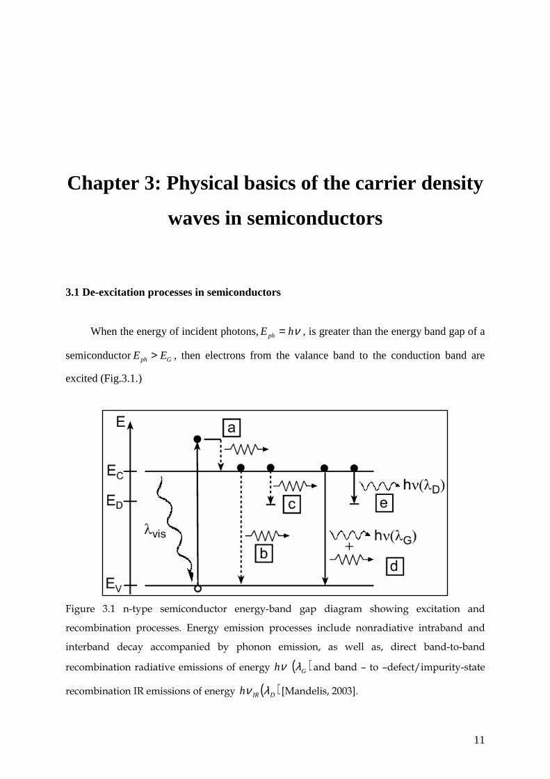
When the energy of incident photons, νhEph = , is greater than the energy band gap of a
semiconductor Gph EE > , then electrons from the valance band to the conduction band are
excited (Fig.3.1.)
Figure 3.1 n-type semiconductor energy-band gap diagram showing excitation and
recombination processes. Energy emission processes include nonradiative intraband and
interband decay accompanied by phonon emission, as well as, direct band-to-band
recombination radiative emissions of energy ( )Gh λν and band – to –defect/impurity-state
recombination IR emissions of energy ( )DIRh λν [Mandelis, 2003].

12
The energy difference GEh −ν is deposed in the kinetics energy of the electrons. This
energy is gradually lost on collisions with other carriers and lattice phonons until thermal
equilibrium is achieved. This process is named the thermalization (process (a) in Fig 3.1) and
as a result creates a heat source and can be accurately described by the optical absorption
distribution [Mandelis, 1998]:
( ) ( )( )rEhvtNtrQ gGIB
rr λαηλ −⋅−= exp)(),,( 0
3m
W, (3.1)
where ),,( λtrQIB
r is the intraband heat release rate per unit volume of the optically excited
semiconductor, Gη is the quantum efficiency for photogenerated carriers, ( )λα is the optical
absorption coefficient at the excitation wavelength λ, and ( )tN0 is the photon deposition rate
per volume. Assuming an average intraband relaxation time to be in order of 10-12 [s]
[Bandeira et al.,1982], effects due to intraband thermalization may be neglected on the time
scale of the conventional frequency domain photothermal response of the semiconductor as is
seen in Figure 3.2. Figure 3.2 shows discussed de-excitation processes as a function of time.
Figure 3.2 De-exctitation processes in semiconductor as a function of time.
After the thermalization electron (hole) to the bottom (the top) of the conduction band
(the valance band) electrons and holes create electron-hole pairs. The energy of these pairs
can be changed to other existing type of energy (as e.g. heat) on several processes depending
on the type of the energy bandgap (direct or indirect), defects and/or concentration of these
pairs. Photo-exited carriers can diffuse (process 3 in Figure 3.2) through a distance called a

13
diffusion length jjj DL τ= (where j=n (electron) or p (hole)) and then recombine
radiatively or non-radiatively through the energy bandgap (processes b and d in Figure 3.1
and process 4 in Figure 3.2) with respect to theirs lifetime τ which can be written
NRR τττ111 += , (3.2)
where τR and τNR are lifetimes related with radiative and non-radiative processes, respectively.
In a semiconductor with a direct bandgap (e.g. CdSe) the emission of photons is a result of the
radiative recombination of photo-excited pairs (in fact in CdSe electrons and holes create an
excition). In case of semiconductors with an indirect energy bandgap (as silicon or
germanium) the emission of photons is accompanied with phonons (process d on Figure 3.1).
It is also non-zero probability that excess electron-hole pairs can recombine through non-
radiative bulk interband transition whence generate a heat source [Quimby et al., 1980]. The
heat release rate per unit volume due to non-radiative recombination is given according
Bandiera et al. [Bandiera, 1982], Thielemann and Rheinlaender [Thielemann et al., 1985] by:
( ) ( ) ( )( )rEtNtrQ GNRGBB
rr λαηηλ −= exp;, 0 , only relevant when GEh ≥ν
3m
W (3.3)
where NRη is the non-radiative quantum efficiency.
Besides above discussed processes photo-excited carriers can nonradiatively recombine
at the semiconductor surface generating another heat source. This surface heat release rates
per unit area is given by Flasier and Cahen [Flasier et al, ] and Bandeira [Bandiera et al.,1982]
for a front surface:
( ) ( )[ ] GFSFSFS ESNtNtQ 0,,0,,0 −= ληλ (3.4a)
and for a rear surface:
( ) ( )[ ] GBSBSBS ESNtLNtLQ 0,,,, −= ληλ (3.4b)
where FSη ( BSη ) is the front (rear) surface non-radiative quantum efficiency, ( )λ,,0 tN is the
photogenerated electron density distribution in a one dimensional geometry, N0 is the
equilibrium density, and SFS [m/s] (SBS) is the front (rear) recombination velocity. Both
surface recombination velocities are parameters which characterize the density of the surface
defect states. When S=0 the surface retains bulk properties. When S>0 the surface acts as a
sink for photogenerated carriers. Values of S in the range 1000 <≤ S [cm/s] generally
indicate good passivation for silicon surface [Guidotii et al. 1989].

14
3.2 Ambipolar diffusion equation
At the point r in a semiconductor, the time rate of change in the concentration N(r,t) of
the excess electron-hole pairs is governed by both diffusion and recombination, and can be
described by an ambipolar diffusion equation of the form [Sze, 1981]:
( ) ( ) ( ) ( ) ( )trgtrNtrBNtrN
t
trNtrND ,,,
,,),( 322* rrr
rrrr
=−−−∂
∂−∇ γτ
(3.5)
where ( )trg ,r
is the carrier generation rate per unit volume from an external source of
excitation and *D is an ambipolar diffusion coefficient defined by
( )he
Bhe q
Tk
Dµµ
µµ
+
=2
* (3.6)
where µe and µh are an electron and a hole mobility, respectively. The others parameters from
Eq. (3.5) will be discussed in Section 3.6.
The ambipolar diffusion equation can be linearized when the excess carrier density is
sufficiently small. For example in silicon with the concentration up to 17101×=N [cm-3]
Guidotti et al. [Guidotti et al.,1989] found that τ
γ NNBN <<32 ~ and eq. (3.5) can be written
as
( ) ( ) ( )trgtrN
t
trNtrND ,
,,),(2* r
rrrr
=−∂
∂−∇τ
(3.7)
Assuming that the temporal Fournier transform of ( )trN ,r
exist one can write
( ) ( )∫∞
∞−
⋅⋅−⋅= dtetrNrN ti ωω ,,rr
(3.8)
and taking the Fournier transform of Eq. (3.7) yields
( ) ( ) ( ) dtetrgdtetrN
dtet
trNdtetrND titititi
∫∫∫∫∞
∞−
−∞
∞−
−−∞
∞−
⋅⋅−∞
∞−
−=−∂
∂−⋅∇ ωωωω
ττ,
,,1),(*2 r
rrrr
(3.9)
Follow by Mandelis [Mandelis, 2001] an integration by parts in the second term on the left-
handside (l.h.s) and using the boundary condition for ( )trN ,r
at ±∞→t , results in the
transformed equation
( ) ( ) ( )ωωωσω ,1
,),(*
2 rqD
rNrN e
rrrr−=⋅−∇ (3.10)

15
where the real part of the *
1
D
ie τ
ωτσ += is carrier density-wave wave number, [m-1]. The
CDW wave number is completely different from the thermal wave one. In the case of the
CDW wave number the real and the imaginary parts are unequal. This inequality brings on
that CDW arise only when condition 1≥ωτ is fulfilled.
3.3 One dimensional excess CDW field in Cartesian geometries
Mandelis [Mandelis, 2001] considered the excess CDW field in a semiconductor of the
thickness L. He assumed that the excess carrier distribution is generated according to the
Beer-Lambert Law ( ) ( )tixQ eeh
Ixq ωα
ναη
ω += − 12
, 0 , where β is an absorption coefficient, ηQ is
the quantum yield of the photogenerated carriers, hν is the incident photon energy and I0 is the
optical intensity. Figure 3.3 shows such geometry in one dimension.
Figure 3.3 Illustration of the concept of one-dimensional carrier density wave.
In this one-dimensional geometry, the boundary conditions can be written as
( ) ( ),,0, 10
* ωω NSxNdx
dD
x=
= (3.11a)
16
( ) ( ),,, 1* ωω LNSxN
dx
dD
Lx=−
= (3.11b)
where S1 and S2 are the surface recombination velocities on the two bounding surfaces x=0
and x=L, respectively.
Mandelis [Mandelis, 2001] used a Green Function Formalism to solve Eq. (3.10). The
resulting excess CDW field is
( )( ) ( )
−
Γ−Γ−+
Γ−ΓΓ−Γ
−= −−−
−
−−−
−
+−LxL
L
Lx
L
L
e
Q eee
ee
e
e
Dh
IxN e
e
e
e
e
eασ
σ
σασ
σ
ασ γγγγσαν
αηω )2(
212
212
12
121222*
0
2),(
(3.12)
where
1
11 SD
SD
e
e
+−=Γ ∗
∗
σσ
(3.13a),
2
22 SD
SD
e
e
−+=Γ ∗
∗
σσ
(3.13b),
1
11 SD
SD
e ++= ∗
∗
σαγ (3.13c)
and 2
22 SD
SD
e −−= ∗
∗
σαγ (3.13d)
3.4 Three dimensional CDW field in cylindrical geometries
Mandelis [Mandelis, 2001] deduced that the full three-dimensional cylindrically
symmetric photo-excited carrier-density-wave field in a cylindrical domain of infinite lateral
dimensions, which is generated by a Gaussian source, such as TEM00 laser beam of spot size
W, is given by the solution of a one-dimensional carrier density wave field generated by a
uniform source producing the same incident optical flux under the same boundary condition,
according to the operational transformation
( ) ( )[ ] ( ) λλλωλξσωλ
drJezNWzrNW
eeDD ∫∞
−→=
0
02
12
3
2
,,2,, (3.14)
where ( ) 22, ee σλωλξ += .
Based on the presented theorem the three dimensional expression of the excess carrier density
wave field in an electronic laterally infinite solid of thickness L can be easily obtained by
means of Eq. (3.12). The three dimensional geometry is presented in figure 3.4 where a free

17
carrier density flux is generated by a normally incident Gaussian laser beam of a spot size W.
The incident photons with energies hν cause the absorption and CDW generation which is
occurred according to the Beer-Lambert Law:( ) ( )tiz
W
rQ eeh
IrQ ωα
ναη
ω +=−−
12
,2
2
0 .
Figure 3.4 Illustration of the concept of three-dimensional carrier density wave.
Putting Eq.(3.12) to the Eq.(3.14) one can obtain the expression for three dimensional excess
CDW
( ) ( )
( )( )
∫∞
−
−−−−
−−−
−
+−
−
−
−−
+
−−
=0
0
22
4)2(
212
212
12
1212
*
0 ...
2),,(
22
λλλ
ξαν
αηω
λ
αξξ
ξαξ
σ
αξ
drJ
eee
egg
egge
eGG
eGggG
Dh
IzrN e
W
zxL
L
Lz
L
L
Qe
e
e
e
e
e
(3.15)
where J0(λr) is the Bessel function of first kind of order 0 and
1
11 SD
SDG
e
e
+−= ∗
∗
ξξ
(3.16a),
2
22 SD
SDG
e
e
−+= ∗
∗
ξξ
(3.16b),
1
11 SD
SDg
e ++= ∗
∗
ξα
(3.16c)
and 2
22 SD
SDg
e −−= ∗
∗
ξα
. (3.16d)
18
3.5 Recombination processes in semiconductors
Photoexcitated carriers in semiconductors can recombine by one of three mechanisms
[W.M.Bullis and H.R.Huff, 1996]: a Shockley-Read-Hall (SRH) recombination which is
related to multi-phonon release [W.Shockley and W.Read, 1952 and R.Hall 1952]; photon
release (radiative recombination) and Auger recombination, in which the recombination
energy is carried away by a third carrier.
Assuming that trapping is negligible, so the number of excess holes ),( trPr
is equal the
number of excess electrons ),( trNr
, the total bulk recombination rate Rtotal, will be the sum of
individual rates and the average carrier lifetime can be expressed as
111
1−−− ++
=∆=AugerradSRHtotalR
N
ττττ (3.17)
The SRH lifetime can be reproduced from [W.Shockley and W.Read, 1952] for one existing
dominant center:
( ) ( )NPN
PPPNNN NPSRH ∆++
∆+++∆++=00
100100 τττ (3.18)
where N0 and P0 are the equilibrium electron and hole densities, respectively. Here N1 and P1
are the equilibrium carrier densities related with energy of the defect center ED coincides with
the Fermi level and can be written as
( )
kTNN
TC EE
C
−−
= exp1 (3.19a)
( )
kTNP
VD EE
V
−−
= exp1 (3.19b)
where NC and NV are the densities of states in the conduction and valance band, respectively.
EC and EV are the energies of the conduction and valance band edge, respectively, k is the
Boltzmann constant, and T is the temperature. The time constant for capture of an electron
(hole) by an empty (full) defect state given by
thNDN N υσ
τ 10 = (3.20a)
thPDP N υσ
τ 10 = (3.20b)

19
where ND is the density of defect states. Nσ and Pσ are the capture cross sections for electrons
and holes by the defect, and thυ is the thermal velocity of carriers. The thermal velocity of
carriers is depend on temperature and is expressed by
m
kTth π
υ 8= (3.21)
where m is a mass of an electron.
The second mechanism of recombining carriers is related with a radiative recombination
lifetimes. In semiconductors with direct band gap transition of excited electrons from
minimum of conduction band to maximum of valance band (band-to-band) is more probable
than in the case of semiconductor with indirect energy band gap such as silicon. The
probability of this transition for both types of the semiconductors, with direct and indirect
energy band gap, can be described by the radiative recombination probability B which is
related to recombination lifetime in formula [Varshni, 1967]
( )NPNBrad ∆++=
00
1τ (3.22)
The coefficient B for semiconductors with indirect energy band gap is in order of 10-15
[Varshni, 1967; Gerlach et al., 1972; Augustine et al. 1992] while for direct energy band gap
semiconductor is 10-9 [cm3/s].
The recombination lifetime expression in the case of Auger recombination can be
written as [Schroder, 1998]
( ) ( )20
20
20
20 22
1
PPNNCNNPPC NPAuger ∆+∆++∆+∆+
=τ (3.23)
where CP and CN are the Auger coefficient for holes and electrons, respectively. In highly
doped silicon those coefficients were found by Dziewoir and Schmid [Dziewoir and Schmid,
1977]: 31108.2 −×=NC 32109.9 −×=PC [cm6/s].
For demonstration purposes one can calculate recombination lifetimes for p-type silicon is
shown in Figure 3.5 as a function of injection level for assumed defect level in the middle of
the band gap and the following parameter values: 31108.2 −×=NC 32109.9 −×=PC [cm6/s],
15104 −×=B [cm3/s], 14101 −×== NP σσ [cm2], 71007.1 ×=thν [cm/s],
191086.2 ×=CN , 19101.3 ×=VN , 1210=TN [cm-3], 562.0=TE [eV]and 1510== AA Np [cm-3]
which corresponds to a resistivity of approximately 15 Ωcm.

20
1015 1016 1017 1018 1019 102010-11
10-9
10-7
10-5
10-3
10-1
101
SRH radiative Auger total
Rec
ombi
natio
n Li
fetim
e [s
]
Carrier Injection level [cm-3]
Figure 3.5 Calculated recombination lifetimes in silicon as a function of injection level
for a p-type Si wafer with a doping density 1510== AA Np [cm-3]. Assumed
parameter values are given in the text.
It is clear seen that the radiative recombination lifetime is much longer than the SRH or Auger
recombination time constant and has negligible effects on the overall recombination rate. For
low injection level (of an order 1710 [cm-3]) the recombination processes are dominated by
the SRH recombination time constant while at higher injection level by the Auger
recombination time constant.

21
Chapter 4: Experimental methods, signal
generation mechanisms and instrumentation of
PCR and PPE methods
4.1 The Photocarrier Radiometry signal generation mechanism and instrumentation
4.1.1. Introduction
Mandelis et al. [Mandelis et al., 2003] proposed a new technique for the measurement of
the carrier-density – wave and named it the Photocarrier Radiometry (PCR). A modification
of this technique is the room- or high temperature near infrared photoluminescence (NIR-PL).
In the past the NIR-PL has been associated with the presence of impurities or defects and
band-to-band recombination [King and Hall, 1994, Haynes 1956; Varshni 1967].

22
4.1.2. Contribution to the PCR signal
The PCR is associated with room- or high temperature near infrared photoluminescence.
In Figure 4.1 one can see that the photoluminescence spectrum of silicon at room temperature
has two peaks [King and Hall, 1994] The first at 1.09 eV (≈ 1.14 µm) is associated with band
– to – band transitions [Haynes 1956; Varshni 1967]. The second one is an approximately at
0.73 eV (≈ 1.6 µm) and is observed only for silicon wafers grown by Czochralski method and
is associated with oxygen dependent defects complexes [Kitgawara 1992; King and Hall,
1994].
Figure 4.1 Measured photoluminescence spectra at T=30, 130 and 300 K for
Czochralski-grown Si annealed at T=450 C. The data were obtained using a Ge
photodetector [King and Hall, 1994].
The PCR signal theory was discussed thoroughly by Mandelis et al. [Mandelis et al., 2003].
They authors considered an elementary slice of thickness dz, centered at depth z in a
semiconductor slab supported by a backing, but not necessarily in contact with the backing,
Fig 4.2.

23
Figure 4.2 Cross-sectional view of contributions to front-surface radiative emissions
of IR photons from (a) a semiconductor strip of thickness dz at depth z; (b) reentrant
photons from the back surface due to reflection from a backing support material; (c)
emissive IR photons from the backing at thermodynamic temperature T. The carrier-
wave depth profile results in a depth dependent IR absorption/emission coefficient
due to free carrier absorption of the infrared photon fields, both ac and dc [Mandelis,
2003].
A modulated laser beam at angular frequency ω=2πf and wavelength λvis impinges on the
front surface of the semiconductor. The super-bandgap radiation is absorbed within a (short)
distance from the surface and excited carriers are subjected to several de-excitation processes
discussed in Chapter 3. At thermal and electronic equilibrium, a detailed consideration of all
IR emission, absorption, and reflection processes [Mandelis, 2003] yields an expression for
the total IR emissive power at the fundamental modulation frequency across the front surface
of the material in the presence of a backing support which acts both as reflector of
semiconductor-generated IR radiation with spectrum centered at λ. Instrumental filtering of all
thermal infrared emission contributions and bandwith matching to the IR photodetector
allows for all Planck-mediated (8-12 µm) terms to be eliminated and the PCR signal can be
written follow as.[Mandelis, 2003]
( ) ( )[ ] ( )[ ] ( )[ ] ( ) ( )∫ ∫++−=2
1 0
11 ,,111λ
λ
λωεληλλλλωL
fceRRbPCR dzzWRRRdS (4.1)
24
where R1 is the front surface reflectivity, Rb is the backing support material reflectivity, εfc is
the IR emission coefficient due to the free photoexcited carrier wave, WeR(λ) is the spectral
power per unit wavelength, the product to the recombination transition rate from band do
band or from bandedge to defect or impurity state, as the case may be, multiplied by the
energy difference between initial and final states, ηR is the quantum yield for IR emission
upon carrier recombination into one of these states.
For a semiconductor which is in thermal and electronic equilibrium with its environment
Kirchhoff’s theorem is fulfilled:
( ) ( )λωαλωε ,,,, zz fcIRfc = , (4.2)
where αfc is absorption coefficient due to the free photo-excited carriers.
For relatively low carrier densities the absorption coefficient depends on the free carrier
density as [Smith, 1978]
( ) ( )λωµεπ
λλωα ,,4
,,2*3
02
2
zNnmc
qzfcIR ∆= . (4.3)
Putting (4.3) into Eq. (4.1) one can write the expression for the PCR signal in one dimension
( ) ( ) ( )∫∆=L
PCR dzzNFS0
21 ,, ωλλω , (4.4)
where ( ) ( )[ ] ( )[ ] ( )[ ] ( ) ( ) λλληλλλλλλ
λ
dCWRRRF eRRb∫ ++−=2
1
1121 111, .
4.1.3. Instrumentation and normalization of PCR signals
Four photocarrier radiometric systems have been used. The first was related with study
of the effect of the space charge layer on the PCR signal system and the results are presented
in Chapter 6. The second and third systems were constructed in the Center for Advanced
Diffusion Wave Technologies, University of Toronto, Canada [Shaungnessy, 2005] and were
used for the study of the influence of the optical excitation intensity on the PCR signal
(Chapter 7). The last one is the PCR microscope constructed in order to monitor the ion
implanted process in silicon wafers. The common part of all these systems is an InGaAs p-i-n
photodetector (Thornlabs model PDA 400) with the following parameters: spectral bandwidth
of 700-1800nm; an active area of 0.8 mm2, and an adjustable transimpedance gain; the unit
was used at the intermediate gain setting (1.5 ×10⁵ V/A) at which it has a noise equivalent
power (NEP) of 3.8 ×10⁻¹² W Hz-1/2 (at 1310 nm) and a frequency bandwidth of 700 kHz) a
long-pass filter (Spectrogon model LP-1000: a steep cut-on (5% at 1010 nm, 78% at 1060

25
nm) and a transmission range 1042 – 2198 nm is placed in front of the detector in order to
ensure that any diffuse reflections of the excitation source do not contribute to the signal). The
spectral responsivity is shown in Fig 4.3.
Fig 4.3 Spectral responsivity of the PCR detector.
All frequency dependent measurements were normalized by the corresponding wide-
bandwidth instrumental transfer functions. The transfer functions were obtained by measuring
the amplitude and phase of modulated laser radiation scattered from a microscopically rough
metallic surface positioned at the focal plane of the parabolic mirror, and partly transmitted
through the filter.
4.1.4. The one dimensional Photocarrier Radiometry (PCR) Signal
The PCR signal in one dimensional geometry (as this from Figure 3.3) can be written
with help of Eq. (4.4) and Eq. (3.12)
( ) ( ) ( ) ( ) ( ) ( )∫ =∆=L
DDD MEFdxxNFS0
1121211 ,,, ωωλλωλλω (4.5)
where
( ) ( )( )22*
01 2
1
eD Dh
RIE
σανηαω
−−= (4.6)
( ) ( ) ( ) ( )LeL
LLL
D ee
eeeM
e
eeα
σ
ασασ
ασγγω −
−
−+−−
−−Γ−Γ
+Γ−+Γ= 12
12
)(1221
1 (4.7).

26
For silicon wafers, this equation has been applied with superband-gap radiation of absorption
coefficient α(hν) > 103 cm-1, such that the semiconductor material is entirely opaque to the
incident radiation, and thus e-αL ≈ 0. The quantities in (4.6) and (4.7) were defined in Chapter
3 (Eqs.: 3.13 a-d). Using MATLAB program and equation (4.5) simulations of the electronic
parameters on the PCR signal were performed.
10 1 10 2 10 3 10 4 10 510 18
10 19
10 20
10 21
10 1 10 2 10 3 10 4 10 5
-80
-60
-40
-20
0 τ
n=5 µ s
τn=50 µ s
τn=100 µ s
τn=500 µ s
τn=1000 µ s
PC
R A
mpl
itude
[a.u
.]
F re qu e nc y [H z ]
τn= 5 µ s
τn= 50 µ s
τn= 100 µ s
τn= 500 µ s
τn= 1000 µ s
PC
R P
hase
[deg
.]
F req u en c y [H z ]
Figure 4.4 The PCR Amplitude (a) and Phase (b) of p-type silicon wafer versus modulation
frequency with the different values of minority bulk recombination lifetime. Parameter
settings: S1=300cm/s, S2=105 cm/s, Dn* = 30 cm2/s, L = 550 µm, α(λ=514nm) = 7.76×103 cm-1.
Figure 4.4 shows a behavior of the PCR amplitude (a) and phase (b) for a silicon wafer with
the minority recombination lifetime τn in the variations in the range 5 µs ≤≤ nτ 1 ms. A
decrease in τn diminishes the PCR amplitude and shifts the position of the turning point
(“knee”) to higher frequencies as the density of the carrier-wave over one period decreases
with decreasing recombination time [Mandelis, 2001]. The PCR phases exhibit zero delay
with respect to the modulation source at low frequencies, such that ωτn << 1 but they begin to
lag behind the source phase as soon as this condition is not valid. As τn decreases, the
foregoing condition becomes violated at progressively higher frequencies, whence the shift of
the PCR phases in Fig. 4.4b [Mandelis et al., 2003].

27
101 102 103 104 105
-80
-60
-40
-20
0
101 102 103 104 105
1019
1020
D*
n=5 [cm2/s]
D*
n=10 [cm2/s]
D*
n=20 [cm2/s]
D*
n=30 [cm2/s]
D*
n=45 [cm2/s]
PC
R P
hase
[deg
.]
Frequency [Hz]
D*
n=5 [cm2/s]
D*
n=10 [cm2/s]
D*
n=20 [cm2/s]
D*
n=30 [cm2/s]
D*
n=45 [cm2/s]
PC
R A
mpl
itude
[a.u
.]
Frequency [Hz]
Figure 4.5 The PCR Amplitude (a) and Phase (b) of p-type silicon wafer versus
modulation frequency with the different values of ambipolar diffusivity. Parameter
settings: τn = 100 µs, S1 = 300 cm/s, S2 = 105 cm/s, L = 550 µm, α(λ=514nm) =
7.76×103 cm-1
Figure 4.5a shows the change in the PCR amplitudes affected by altering the
ambipolar diffusivity Dn*. If Dn
* is controlled by the bulk of the semiconductor, then an
increase of this quantity will decrease the PCR amplitude. This behavior can be explained by
the fact that the CDW “centroid” – center of the charge carriers - shifts away from detection
point at surface therefore the contribution of the recombining carrier density wave to the PCR
signal generated at the surface (or/and subsurface) is smaller. At low frequency the PCR
phase doesn’t show any lag, until 1>>ωτ is fulfilled, then an onset of the PCR phase lag is
observed. The PCR phase lag exhibits a shift to higher frequencies with increasing Dn*. High
frequencies can affect the position of the CDW centroid shifting it to smaller depth. This
effect is observed on the PCR amplitude and the PCR phase.

28
101 102 103 104 105
1019
1020
101 102 103 104 105-100
-80
-60
-40
-20
0
S1=0 [cm/s]
S1=0.1 [cm/s]
S1=1 [cm/s]
S1=10 [cm/s]
S1=1000 [cm/s]
P
CR
Am
plitu
de [a
.u.]
Frequency [Hz]
S1=0 [cm/s]
S1=0.1 [cm/s]
S1=1 [cm/s]
S1=10 [cm/s]
S1=1000 [cm/s]
PC
R P
hase
[deg
.]
Frequency [Hz]
Figure 4.6 The PCR Amplitude (a) and Phase (b) of p-type silicon wafer versus
modulation frequency with the different values of front recombination velocity.
Parameter settings: τn = 100 µs, S2 = 105 cm/s, Dn* = 30 cm2/s, L = 550 µm,
α(λ=514nm) = 7.76×103 cm-1.
Figure 4.6 shows the effect of changing the recombination velocity S1 on the PCR
frequency scans. The PCR amplitudes decrease (fig. 4.6a) as the value of S1 increases. This
behavior is quite similar to the case observed for decreasing of the minority recombination
lifetime τn, although the “knee” shift to higher frequencies is not as pronounced. A similar
behavior is observed for the PCR phases (fig. 4.6b), where the phases lag move to higher
frequencies. Additionally, the phase lag shows gradual decrease with increasing S1 due to the
sub-surface ac diffusion length (or “centroid”) of the CDW which is no longer controlled by
the bulk recombination lifetime τn alone but it becomes controlled by an effective lifetime, τeff,
defined as follows [Mandelis 2005]:

29
speff τττ111 += (4.8)
where τs is the interface lifetime related to the interface recombination velocity S1. This time
constant begins to influence the effective lifetime (and hence the phase saturation level) at S1
values such as τs ~ τn.
Figure 4.7 shows the effect of changing recombination velocity S2 on PCR frequency scans.
101 102 103 104 105-100
-80
-60
-40
-20
0
101 102 103 104 105
1019
1020
S2=0 [cm/s]
S2=0.1 [cm/s]
S2=1 [cm/s]
S2=10 [cm/s]
S2=1000 [cm/s]
PC
R P
hase
[deg
.]
Frequency [Hz]
S2=0 [cm/s]
S2=0.1 [cm/s]
S2=1 [cm/s]
S2=10 [cm/s]
S2=1000 [cm/s]
PC
R A
mpl
itude
[a.u
.]
Frequency [Hz]
Figure 4.7 The PCR Amplitude (a) and Phase (b) of p-type silicon wafer versus
modulation frequency with the different values of rear recombination velocity.
Parameter settings: τn = 100 µs, S1 = 300 cm/s, Dn* = 30cm2/s, L = 550 µm,
α(λ=514nm) = 7.76×103 cm-1.

30
4.1.5. The three dimensional PCR signal
In Chapter 3 (Section 3.4) it was shown that the photo-excited carrier density wave field
in three dimensional cylindrical geometries can be described by: (see Eq. (3.14) )
( ) ( )[ ] ( ) λλλωλξσωλ
drJezNWzrNW
eeDD ∫∞
−→=
0
02
12
3
2
,,2,, (4.9)
where ( ) ( )[ ]2
21
23 ,,2,,
~
−→=
W
eccDD ezNWzNλ
ωλξσωλ is the Hankel transform of Eq. (3.14).
In order to account for contributions over the thickness of the wafer the Hankel transform of
the carrier density field has to be integrated over the depth:
( ) ( )∫=L
DD dzzNN0
33 ,,~
,~ ωλωλ (4.10)
The finite area of the detector must be taken into consideration to account for carrier diffusion
out of the field of view of the collection optics/detector assembly [Shaughnessy, 2005].
Assuming a disc of radius a2 and area A as the effective detector size and using the relation
[Ikari et al., 1999]:
( ) ( ) ( ) ( )∫ =2
0
2132
03 ,~1
,~1
a
DD aJNa
dJNA
λωλλπ
ρρλρωλ (4.11)
where J1is the Bessel function of first kind of order 1. The PCR signal can be expressed in
final form as the inverse Hankel transform of (4.9) integrated over the detector area
( ) ( ) ( )∫∞
=0
2132
3, ,~ λλωλ
πω daJN
a
CS DDPCR (4.12)
where
( ) ( ) ( )ωλωλωλ ,,,~
333 DDD MEN = (4.13)
( ) ( )( )22*
40
3 2
1,
22
e
W
D Dh
eRIE
ξαναηωλ
λ
−−=
−
(4.14)
( ) ( ) ( ) ( )[ ] ( )α
ωλωλξ
ωλα
ξξ L
L
e
L
D
eeCC
eM e
e −−
− −−+−= 1,,
1, 213 (4.15)
( )( )
−−= −
−−
L
L
e
e
eGG
eggGGC ξ
ξα
ωλ2
12
21211 , (4.16)

31
( )( )
L
L
e
e
eGG
eGgGgC ξ
ξα
ωλ2
12
22112 , −
−−
−−= (4.17)
Coefficients in (4.12) - (4.17) were defined in Chapter 3.
4.1.6. The photocarrier radiometry (PCR) dimensionality criterion
Figure 4.8 shows a frequency-scan simulations in two sets of linear PCR signals from
silicon based on 1-D (full lines) and 3-D (squares and rhombs) theoretical models (Eqs 4.5
and 4.10, respectively) with laser wavelength 830 nm, spotsize 4 mm and recombination
lifetimes τ = 20 µs and 800 µs. The optical absorption coefficient was taken to be αP = 635
cm-1. The carrier transport parameters were assumed equal for both sets of curves. The
amplitude curves are normalized to unity at f = 10 Hz.
0.1
1
0.01 0.1 1 10 100-100
-80
-60
-40
-20
0
1-D Simulation τ - 800 µs
1-D Simulation τ - 20 µs
Log(
Am
plitu
de)
[a.u
.]
1-D Simulation τ - 800 µs
1-D Simulation τ - 20 µs
Pha
se [d
egre
es]
Log (Frequency [kHz])
Figure 4.8 PCR frequency scan simulations with short and long carrier recombination
lifetimes using 1-D and 3-D theoretical model. 3-D simulations with τ = 20 µs () and
800 µs (); 1-D simulations with τ = 20 µs (—) and 800 µs (—) coincide with the
corresponding 3-D simulation. Other transport parameters: D = 15 cm2/s, S1 = 200
cm/s, S2 = 105 cm/s, αp = 659 cm-1. Laser beam spotsize: 4 mm.

32
It is clear that the simulations using the 1-D and the 3-D equations coincide, as expected, for
the chosen large spotsizes compared to the maximum carrier-wave diffusion length, LD(ω) = |
σn(ω) |-1 at the lowest frequency f = 10 Hz where LD(10 Hz) =173.2 µm for τ = 20 µs and
1,095 µm for τ = 800 µs. In practice, the use of 1-D theory to explain PCR data is warranted
when a change of the beam spotsize on the semiconductor surface does not produce
measurable change in the PCR phase. This is an important dimensionality criterion, therefore,
the dependence of the PCR phase on laser spotsize using the 1-D or the 3-D theory with
various lifetimes (or diffusion lengths of the photo-excited free carrier density-wave) at two
frequencies is presented in Fig. 4.9.
10 100 1000
-20
-15
-10
-5
0
10 100 1000
-80
-70
-60
-50
-40
-30
-20
-10
0
830 µm387 µm 24 µm
PC
R P
hase
[deg
ree]
Log(Laser Spotsize [µm])
Lifetimes: τ
1 - 1 µs;
τ2 - 20 µs;
τ3 - 50 µs;
τ4 - 200 µs;
ba
830 µm 387 µm24 µm
PC
R P
hase
[deg
ree]
Log(Laser Spotsize [µm])
Figure 4.9 Laser beam spotsize dependence of PCR phases for frequency 1 kHz (a)
and 100 kHz (b) with broad range of lifetimes and otherwise same other transport
parameters: D = 10 cm2/s, S1 = 500 cm/s, S2 = 105 cm/s, αp = 659 cm-1.
It is clearly seen that, for PCR signals with τ = 1 µs, 1-D theory can be used with spotsizes
2W ≥ 387 µm at 1 kHz and 100 kHz. However, with τ = 20 µs, 50 µs, and 200 µs, the
condition 2W ≥ 830 µm is required at 100 kHz. In the latter cases all lower frequency ranges
require a 3-D theoretical approach.

33
4.1.7 Photo-carrier radiometry microscope
In this section the capability of the PCR technique to monitor a quality of ion implanted
wafers is presented. In order to present that PCR signal is sensitive to the change of carrier
transport properties the photocarrier radiometry microscope was constructed and it is
presented on Figure 4.10. As an excitation source of carrier density waves a 808 nm laser
diode (0.5mm beam radius) was used. The power of the laser diode was typically 200 mW.
The diode laser beam was focused onto the sample surface using lens. The position of the
laser beam is coincident with the focal point of an off-axis paraboloidal mirror that collects
a portion of infrared radiation from the samples. The collected light is then focused onto
the detector by means of lens. Sample was placed onto aluminum holder (acted as a
mechanical support and signal amplifier by redirecting the forward emitted IR photons
back toward the detector [Mandelis, 2003]. The x-y position scans were realized by means
of homemade x-y motor stage. All instruments, data acquisition, and data storage are
controlled by a computer running Pascal program with a graphical user interface and real-
time display of experimental data.

34
Figure 4.10. The photocarrier radiometry microscope.
Typical result obtained using modulation frequency 10 kHz for an ion implanted wafer is
presented at Fig. 4.11.
Figure 4.11: The PCR amplitude and phase as a function of x-y-scan of the silicon
wafer implemented with 6.3 1016 doses of protons [cm-2]. Sample preparation: The

35
energy of the protons was 1 MeV with an implantation depth of 18 µm, the beam
was focused on 5x5 mm2 area on the silicon wafer surface.
The squares on Figure 4.11 depict the ion implanted regions. Figure 4.12 shows the PCR
phase as a function of coordinate.
Figure 4.12: The PCR phase a a function of x-scan of the silicon wafer
implemented with 6.3 1016 doses of protons [cm-2] at the difference frequencies.
Sample preparation: The energy of the protons was 1 MeV with an implantation
depth of 18 µm, the beam was focused on 5x5 mm2 area on the silicon wafer
surface.
From Fig. 4.12 one can see that for 1 kHz the PCR technique is unable to detect any
changes in the PCR phase so in the carrier transport properties. Whereas above 1 kHz
changes in the PCR phases are clearly seen. The PCR phase lag was observed in an ion
implanted region. This is can be explained because the photo-carrier diffusion length is too

36
large to detect any inhomogeneous in the free carrier density depth in the implantation
region.
4.2 The photopyroelectric (PPE) signal generation mechanism and instrumentation
4.2.1. Experimental Setup
The PPE measurements were performed in the back detection configuration, where the heat
is generated on the front side of the sample and the temperature oscillations are measured with
the pyroelectric detector contacted to the back side of the sample. The experimental setup
constructed for the back detection configuration is presented in Fig. 4.13.
Figure 4.13: PPE experimental set up
The thermal wave are excited by an argon ion laser with output power 200 mW and
operating wavelength λ = 514 nm. The laser beam of 1.89 mm diameter was intensity modulated
by means of an acousto–optical modulator in the frequency range 1 Hz to 10 Hz and focused onto
the sample. The front surface of the sample was covered by an optically opaque 20 µm to 30 µm
graphite coating. Samples were attached to a pyroelectric detector by means of a grease layer

37
(Apiezon T grease). As the grease layer was very thin, its contribution to the PPE signal could be
neglected. A 0.98 mm thick lead zirconate titanate PZT crystal was used as a pyroelectric
detector. The PPE signal detection was performed by means of a lock-in amplifier (Stanford
830). The detector was placed on a cooper plate with a drilled hole (inside was air). The sample –
detector – copper support assembly was placed in an aluminum chamber. A schematic of the
PPE chamber is presented in Fig. 4.14.
Fig. 4.14: PPE chamber: 1 Peltier-element, 2 aluminum support, 3 cylindrical cooper
support, 4 the PZT detector, 5 sample with optically opaque cover-layer, 6 quartz
window, 7. BNC connector for PPE Signal
The temperature was varied in the range from 20° C up to 40° C by means of a Peltier
element which was driven by a homemade current controller (Appendix A).
4.2.2. The PPE signal generation mechanism.
The average temperature oscillation Tp at angular frequency ω0 in a pyroelectric detector
leads to variations of the surface charge density Q due to the pyroelectric effect and can be
written according to B. R. Holeman [Holeman, 1972] as:

38
( ) ( ) ,0p0 ωω TpQ = (4.18)
where p is the pyroelectric coefficient of the detector. Time-dependent variations of the surface
charge causes a current flow through the detector of the thickness Lp [Mandelis and Zver, 1985;
Rombouts et al., 2005];
( ) ( ) ( ) ( ) ,eed
dd),(
1
d
d
dt
d00
p
0p00pp
0p00
titi
L
ipAt
xxTL
pAt
TpA
QAI ωω ωθωω
ωωω =
=== ∫ (4.19)
where A is the transducer area and ( ) xxTL L
d),(1
p
0pp
0p ∫= ωωθ . Tp(ω0,x) is the temperature field in
the pyroelectric detector.
Figure 4.15 shows a schematic of the sample’s model.
Figure 4.15 Schematic of the sample’s model
39
In the used arrangement the front surface was covered by a 20 µm to 30 µm thick graphite layer
which prevents exciting light to penetrate into the sample. The rear surface was connected to the
detector which monitored the thermal wave transmitted through the sample. The distribution of
the thermal wave is the solution of one-dimensional thermal transport equations as a result of heat
conduction through the sample. Similar theoretical models were considered by Chirtoc and
Mihalescu [Chirtoc and Mihalescu, 1989] and Mandelis and Zver [Mandelis and Zver, 1985]. In
both works the influence of the thermal interface between the rear surface of the sample and the
detector was neglected. Experimentally a good thermal contact was achieved with a very thin
grease layer. As in the presented experiments the thermal waves were generated by surface
heating the contribution to the heat transport problem of the thermally thin graphite surface layer
can be neglected. Also, the thermal contact of the sample to the detector by the grease layer is
considered to be ideal. In some cases, however, the thermal diffusivity Dt of the sample can be
underestimated due to the influence of the grease layer as demonstrated by Salazar
[Salazar,2003]. He calculated the error of the Dt estimation in the presence of about a 2 µm to 3
µm thick grease layer. He found that the error is large for thin and good thermal conductors at
high frequencies and decreases with increasing thickness and decreasing thermal diffusivity of a
material and modulation frequencies. Although in our measurements we used a different grease,
one can deduce that the investigated samples as well as a glassy carbon are rather poor thermal
conductors. Furthermore, this effect is additionally reduced because measurements were
performed at modulated low frequencies. When the sample and the detector are both thermally
thick and optically opaque the temperature field can be obtained using a formula of Chirtoc and
Mihalescu [Chirtoc and Mihalescu, 1989] and Mandelis and Zver [Mandelis and Zver, 1985]:
( ) ,22
exp2
exp
1
ss
0s
s
0
0
sp
ps
p
ps0
+−
−
+
=Θ LD
iLD
Dk
Dkk
Dp
ωπω
ω
ηω (4.20)
where ηs is the nonradiative conversion efficiency of the absorbing layer: The sample is
characterized by a thickness Ls, a thermal diffusivity Ds and a thermal conductivity ks. The
40
detector is characterized by a thermal diffusivity Dp and a thermal conductivity kp. The PPE
signal is then given by
( ) ( ) ( ) ,22
exp2
exp1 s
s
0s
s
0
spp
ps00
+−
−
+= L
DiL
Dbk
DApII
ωπωηω (4.21)
where I0 is the intensity of the optical excitation: The phase of the PPE-signal is given by
.22 s
s
fmLD
f −−=−−= πππϕ (4.22)
The coefficient m can be easily determined from experimental data. Thus, with the known sample
thickness the thermal diffusivity can be deduced by the relation
.2
s2
s m
LD
π= (4.23)
The PPE amplitude can be written as
( )( ) ,2
lns
s2
0s
s2
0 fmBfD
LB
D
LBI −=−=
−+= πωω (4.24)
where
+
=
sp
ps
p
ps0
1
ln
Dk
Dkk
DApIB
η.
4.2.3. Normalization of the PPE Signal
Figure 4.16 shows the PPE amplitude and the PPE phase from the detector alone as a
function of the modulation frequency in the temperature range from 26 °C to 36 ºC. Error bars
for PPE phases were approximately 1.5°.

41
2 4 6 8 10
90
92
94
96
2 4 6 8 101.60E-010
1.65E-010
1.70E-010
1.75E-010
1.80E-010
Frequency [Hz]
26 0C 27 0C 28.5 0C 31 0C 33 0C 36.50C
PP
E p
hase
[deg
]
PP
E a
mpl
itude
[A]
Frequency [Hz]
Fig. 4.16: PPE amplitudes (a) and phases (b) of the detector alone at different
temperatures (in °C).
From the experimental data in Fig. 4.16b, one can see that in the investigated range of the
temperature the PPE phases remains constant within error bars. This means that the thermal
properties of the detector can be assumed constant under our measurement conditions. We had
also observed small changes in the PPE amplitudes, Fig. 4.16a, but these can be caused by the
temperature-dependence of the pyroelectric coefficient and/or thermal effusivity ep (ep = kp(Dp)-
1/2) of the PZT detector as well as long term fluctuations of the laser intensity. These effects can
be minimized by an appropriate normalization procedure. Detenclos et al. [Delenclos et al., 2001]
normalized the PPE signal from an investigated material to the one obtained with the detector
alone or to the signal obtained with a reference sample. They considered the PPE signal for the
sample and the detector both thermally thick and optically opaque and pointed out that the
normalized signal is not influenced by the temperature-dependence of the pyroelectric
coefficient, hence, only a knowledge of thermal effusivity of the detector is required. In fact, PPE
amplitudes were normalized to the reference sample instead of the detector alone as the
absorption of laser light at the detector electrode is different from that in the graphite layer
[Delenclos et al., 2001]. In addition, it is also possible that the heating spot (laser beam spot)

42
interacts (energy exchange) with silver contacts on the surface of the detector, and this could lead
to a worse signal-to-noise ratio (SNR) than in the case of normalization to a reference material.
As a reference sample, a 0.98 mm thick piece of a glassy carbon (type G) was used. The
specific heat capacity C of the glassy carbon in the temperature range from 26 °C to 80 °C was
determined from differential scanning calorimetry (DSC) measurements and these results are
presented in Table 4.1.
Table 4.1 presents the specific heat capacity of the glassy carbon (thickness L=0,98mm)
in different temperatures estimated from the PPE phases and amplitudes and result of
the DSC measurements.
Temperature [°C] The specific heat capacity
C [J/kg°C]
26.85 1054.568
36.85 1064.533
46.85 1151.807
56.85 1268.092
66.85 1397.104
76.85 1510.841
86.85 1612.371
The error limit of the differential scanning calorimetry (DSC) measurements was 3% to
5%. One can see that in the covered temperature range (from 20 to 40° C) the specific heat
capacity C is about 1050 J⋅kg-1⋅K-1 within the error limit.
Figures 4.17a and 4.17b present the PPE signal phases and amplitudes of the glassy
carbon, respectively, at room temperature as a function the square root of the modulation
frequency. It is worthwhile to note that the error bars were approximately 0.5°.

43
1.5 2.0 2.5 3.0 3.5
-1.0
-0.5
0.0
0.5
1.0 1.5 2.0 2.5 3.0 3.5
e-16
e-15
experimental data the best linear fitting
Sqrt(Frequency) / Hz
PP
E P
hase
/ de
g
experimental data the best linear fitting
Sqrt (Frequency) /Hz
ln(A
mpl
itude
)/au
Fig.4.17 The PPE Phase and Amplitude of the glassy carbon (thickness L=0.98µm) as a
function of a square frequency, respectively. The linear fitting of the experimental PPE
Phase to the Eq. 4.22 gives m=-0,860±0,003, whereas the linear fitting of experimental
PPE amplitude to the Eq. 4.24 gives m=0,857±0,001.
Using Eqs. (4.22) and (4.23) the thermal diffusivity from the as measured PPE phases of
the glassy carbon was estimated to Ds = 4.22x10⁻⁶ m2⋅s-1. The same value of the thermal
diffusivity was obtained from the measured PPE amplitudes by Eq. (4.24) and Eq.(4.23). Using
the literature value of the mass-density ρ = 1.42⋅103 kg⋅m-3 [http://www.htw-gmbh.de/] the
thermal conductivity of the glassy carbon type G was calculated to ks = 6.3 W⋅m-1⋅K-1 which is in
excellent agreement with the value deduced from the data sheet of the producer of the glassy
carbon [http://www.htw-gmbh.de/]. This demonstrates the reliability of the present experimental
setup and measurement procedure for the experimental determination of the thermal diffusivity.
Table 4.2 presents temperature dependence of the thermal diffusivity of the glassy carbon
calculated using Eq. (4.22) - (4.23).
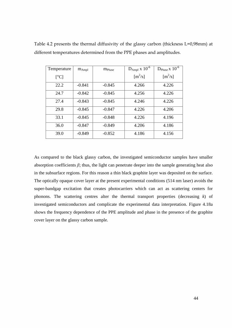
44
Table 4.2 presents the thermal diffusivity of the glassy carbon (thickness L=0,98mm) at
different temperatures determined from the PPE phases and amplitudes.
Temperature
[°C]
mAmpl mPhase DAmpl x 10-6
[m2/s]
DPhase x 10-6
[m2/s]
22.2 -0.841 -0.845 4.266 4.226
24.7 -0.842 -0.845 4.256 4.226
27.4 -0.843 -0.845 4.246 4.226
29.8 -0.845 -0.847 4.226 4.206
33.1 -0.845 -0.848 4.226 4.196
36.0 -0.847 -0.849 4.206 4.186
39.0 -0.849 -0.852 4.186 4.156
As compared to the black glassy carbon, the investigated semiconductor samples have smaller
absorption coefficients β; thus, the light can penetrate deeper into the sample generating heat also
in the subsurface regions. For this reason a thin black graphite layer was deposited on the surface.
The optically opaque cover layer at the present experimental conditions (514 nm laser) avoids the
super-bandgap excitation that creates photocarriers which can act as scattering centers for
phonons. The scattering centres alter the thermal transport properties (decreasing k) of
investigated semiconductors and complicate the experimental data interpretation. Figure 4.18a
shows the frequency dependence of the PPE amplitude and phase in the presence of the graphite
cover layer on the glassy carbon sample.
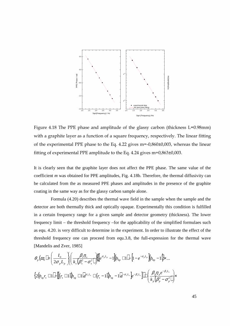
45
1.0 1.5 2.0 2.5 3.0 3.5
e-16
e-15
1.0 1.5 2.0 2.5 3.0 3.5-1.5
-1.0
-0.5
0.0
0.5
Sqrt (Frequency) /Hz
ln(A
mpl
itude
)/au
experimental data the best linear fitting
PP
E P
hase
/ ra
d
Sqrt(Frequency) / Hz
Figure 4.18 The PPE phase and amplitude of the glassy carbon (thickness L=0.98mm)
with a graphite layer as a function of a square frequency, respectively. The linear fitting
of the experimental PPE phase to the Eq. 4.22 gives m=-0,860±0,003, whereas the linear
fitting of experimental PPE amplitude to the Eq. 4.24 gives m=0,863±0,003.
It is clearly seen that the graphite layer does not affect the PPE phase. The same value of the
coefficient m was obtained for PPE amplitudes, Fig. 4.18b. Therefore, the thermal diffusivity can
be calculated from the as measured PPE phases and amplitudes in the presence of the graphite
coating in the same way as for the glassy carbon sample alone.
Formula (4.20) describes the thermal wave field in the sample when the sample and the
detector are both thermally thick and optically opaque. Experimentally this condition is fulfilled
in a certain frequency range for a given sample and detector geometry (thickness). The lower
frequency limit – the threshold frequency –for the applicability of the simplified formulaes such
as equ. 4.20. is very difficult to determine in the experiment. In order to illustrate the effect of the
threshold frequency one can proceed from equ.3.8, the full-expression for the thermal wave
[Mandelis and Zver, 1985]
( ) ( ) [ ]( ) [ ]( ) (
×−−−+−
−
= − ...1111
2 220
0 bpL
bpL
sss
ss
ppp bebe
kL
Ipppp σσ
σβηβ
σωθ
( ) ( )( ) ( )( )[ ][ ]) ( ) ×
−+−−+++−+
−−−
22111112
ppp
LppLL
sgsL
sgsssg k
eeebrebrrb
ss
ssssss
σβηβ β
βσσ
46
]( ) ]( )[ ( ) ]( ) [ ][[([ ×−++−++−−−+− −− pppppppp L
ps
L
rpsbp
L
bp
L eberbbebe σσσσ 11111111
( )( ) ) ( )( ) ( )( ) [ ]]×−−−+++−−− −−− pppppppp LLbsbp
Lbsbp
p
Lpbpps eebbebb
rerbb βσσβ 11111
11
( ) [ ]( ) [ ] ( )([ ( ) [ ] ( )+−−+−−−−+−++ − 11111111 psL
ppsbpL
bpLL
sg berbbebeeb ppppppssσσσσ
[ ]( )( ) ) ( )( ) ( )( ) ×+−+−+−−+− −−− pppppppp Lpsbp
Lpsbp
p
Lpbpps
Lebbebb
rerbbe
σσβσ 11111
11
[ ]]( ) ( )( )( ) ( )( )[ ]( +−−++++÷−− −−−ssppppsspp LL
psbpL
psbpsgL
sgL eebbebbbebe σσσσβ 1111111
( )( )( ) ( )( )[ ] )sspppp LLpsbp
Lpsbpsg eebbebbb σσσ −−+−+−+− 11111 (4.25)
where ( ) jj ai+= 1σ
nn
mmmn ak
akb =
( )ssLX σexp=
( )spLY σexp=
( )( )psp LLZ += σexp
( )220
2 sss
ss
k
IE
σβηβ−
=
( ) ( )( )spsppp
pp Lk
IF ββ
σβηβ
−−−
= exp2 22
0
Substituting Eq. (4.25) into Eq.(4.21) one obtains a full expression for the PPE signal.
Figure 4.19 presents the frequency dependence of the numerical simulations of the PPE
amplitudes with thermal properties of the detector as parameters. The normalized amplitudes and
phases of the PPE signal were simulated numerically using MATLAB program and Eq. (4.25). The
glassy carbon was used as a reference sample.
=
thj D
a2
0ω
j
jjr
σβ
=

47
0 1 2
-0.6
-0.4
-0.2 α
p=10 -7[m/s],k
p=0.9[W /mK]
αp=10 -7[m/s],k
p=0.9[W /mK]
αp=5x10 -7[m/s],k
p=1.13[W /mK]
αp=5x10 -7[m/s],k
p=1.13[W /mK]
αp=8x10 -7[m/s],k
p=1.6[W /mK]
αp=8x10 -7[m/s],k
p=1.6[W /mK]
ln(N
orm
aliz
ed P
PE
Am
plitu
de[a
.u.])
Frequency1/2[Hz1/2]
Fthreshold
Figure 4.19: Numerical simulations based on equ. (4.25) (lines) and equ (4.20)(scatters) of
normalized PPE amplitudes as function the square root of the modulation frequency for
different thermal properties of PZT detector. The others parameters are: Lp=0.98 mm,
Ls=1.325 mm, Lr=0.98 mm, Ds=4.8 10-6 [m/s], Dr=4.2 10-6 [m/s], Dg=2.2 10-5 [m/s],ks=9
[W/mK], kr=6.3 [W/mK], kr=0.026 [W/mK],αs=106[1/m], αr=106 [1/m].
It is clearly seen that the threshold frequency Fthreshold (indicated in Figure 4.19) is independent of
the thermal properties of the PZT detector. Changes of the magnitude of the normalized PPE
amplitude are unfavorable when the thermal conductivity has to be determined. From Figure 4.19
it is evident that the normalization procedure doesn’t solve this problem in the used range of the
thermal properties. In fact, comparing Fig. (4.16) and Fig. (4.19) one can deduce that in limited
temperature range around room temperature the thermal properties of the detector don’t change
much and so their influence on the normalized PPE amplitudes can be neglected.
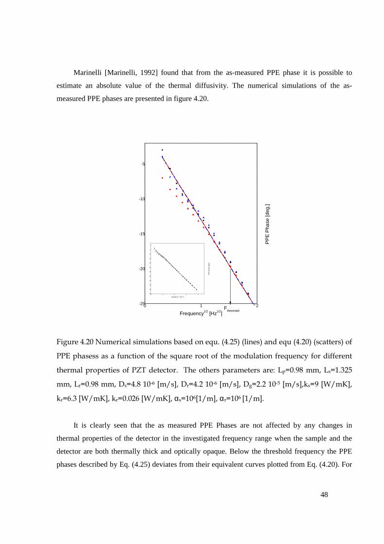
48
Marinelli [Marinelli, 1992] found that from the as-measured PPE phase it is possible to
estimate an absolute value of the thermal diffusivity. The numerical simulations of the as-
measured PPE phases are presented in figure 4.20.
0 1 2-25
-20
-15
-10
-5
0 1 2 3 4-55
-50
-45
-40
-35
-30
-25
-20
-15
-10
-5
0 PP
E P
hase
[deg
.]
Frequency1/2 [Hz1/2]
PP
E P
hase
[deg
.]
Frequency1/2 [Hz1/2]
Fthreshold
Figure 4.20 Numerical simulations based on equ. (4.25) (lines) and equ (4.20) (scatters) of
PPE phasess as a function of the square root of the modulation frequency for different
thermal properties of PZT detector. The others parameters are: Lp=0.98 mm, Ls=1.325
mm, Lr=0.98 mm, Ds=4.8 10-6 [m/s], Dr=4.2 10-6 [m/s], Dg=2.2 10-5 [m/s],ks=9 [W/mK],
kr=6.3 [W/mK], kr=0.026 [W/mK], αs=106[1/m], αr=106 [1/m].
It is clearly seen that the as measured PPE Phases are not affected by any changes in
thermal properties of the detector in the investigated frequency range when the sample and the
detector are both thermally thick and optically opaque. Below the threshold frequency the PPE
phases described by Eq. (4.25) deviates from their equivalent curves plotted from Eq. (4.20). For

49
this reason the m coefficient for glassy carbon were determined in the frequency range from 2 to
10 Hz.
Comparing Fig. (4.19) and Fig.(4.20) one can conclude that the threshold frequency is
more less the same for normalized PPE amplitudes and as measured PPE phases.

50
Chapter 5: Thermal properties of Cd1-xMgxSe
single crystals measured by means of
photopyroelectric technique.
5.1. Materials: Cd1-xMgxSe single crystals
Cd1-xMgxSe single crystals were grown by the high-pressure Bridgman method without
seed under an argon overpressure [F. Firszt et al., 1995]. The mixture of CdSe and metallic Mg
was put into a graphite crucible. The purity of CdSe and Se reaction components was 6N that of
Mg was 99.8 %. The temperature of the heating zone was kept at (1880 ± 0.5) K. The crucible
was held at that temperature for 2 h and then moved out from the heating zone with lowering
speed 4.2 mm⋅h-1. The obtained crystals were cylinders with raw dimensions 8 mm to 10 mm in
diameter and 40 mm to 50 mm in length. The crystals have a longitudinal gradient of magnesium
concentration (Mg content increases from the tip to the end of the crystal). For a crystal with x =
0.3, the Mg concentration gradient is about 0.01 cm-1. The crystals exhibit the wurtzite structure.
The lattice constant of Cd1-xMgxSe crystals decreases with increasing Mg content [F. Firszt et al. ,
1998]. The crystals were cut perpendicular to the growth direction into 0.9 mm to 1.5 mm thick
plates. Next the plates were mechanically polished and chemically etched in a mixture of

51
K2Cr2O7, H2SO3, and H2O in the proportion 3:2:1. Then they were treated in CS2 and hot 50 %
NaOH solution and finally rinsed in water and ethyl alcohol.
Table 5.1: Basic information of Cd1-x MgxSe single crystals.
Sample Technological
Number
Magnesium concentration,
x (mole fraction)
Thickness, L (mm)
1 A423_10 0.00 1.325
2 A557_III 0.00 0.923
3 A558_2 0.06 1.043
4 A440A_VI 0.14 1.306
5 A559_3 0.15 0.944
6 A433_XIV 0.33 1.174
7 A424A_X 0.36 1.294

52
5.2. Experimental results and computational algorithm
5.2.1 Thermal diffusivity – PPE Phases
Figure 5.1 shows experimental phase lags of investigated mixed semiconductors as a
function of the square root of the modulation frequency.
1.2 1.4 1.6 1.8 2.0 2.2 2.4 2.6 2.8 3.0 3.2
-3.5
-3.0
-2.5
-2.0
-1.5
-1.0
-0.5
0.0
Sample 1 Sample 2 Sample 3 Sample 4 Sample 5 Sample 6 Sample 7 Sample 1 Sample 2 Sample 3 Sample 4 Sample 5 Sample 6 Sample 7
PP
E p
hase
, rad
ians
Frequency1/2, Hz1/2
Fig. 5.1: Experimental PPE phase lags (scatters) of the investigated crystals with linear
fittings (lines) vs. square root of the modulation frequency. The fitting parameters are
collected in Table 5.2.
The thermal diffusivities reported in Table 5.2 were calculated using Eq. (4.23) by fitting the as–
measured PPE phases, from Fig. 5.1, with Eq. (4.22).

53
Table 5.2 Results of linear fits to Eq. (4.22) and calculated values of the thermal
diffusivities of Cd1-xMgxSe mixed crystals from Eq. (4.23).
Sample Magnesium
concentration, x (mole
fraction)
Thickness,
L (mm)
m Thermal diffusivity D
(10-6 m2⋅s-1)
1 0.00 1.325 -1.08 4.73
2 0.00 0.923 -0.77 4.48
3 0.06 1.043 -1.26 2.15
4 0.14 1.306 -1.79 1.67
5 0.15 0.944 -1,34 1.58
6 0.33 1.174 -1.85 1.26
7 0.36 1.294 -2.12 1.17
From Table 5.2 it is clearly seen that with increasing magnesium concentration the thermal
diffusivity decreases markedly. Figure 5.2 shows experimental data and theoretical curves of the
temperature dependence of thermal diffusivities for the investigated crystals. The fits assume a
linear temperature variation Dt(T)=aT.

54
20 22 24 26 28 30 32 34 36 38 40 42 441.0
1.5
2.0
2.5
3.0
3.5
4.0
4.5
5.0
Sample 1,a=-0.04 Sample 2,a=-0.04 Sample 3,a=-0.01 Sample 4,a=-0.006 Sample 5,a=-0.006 Sample 6,a=-0.006 Sample 7,a=-0.006
T
herm
al d
iffus
ivity
, x 1
0-6 m
2 ·s-1
Temperature, °C
Fig. 5.2: Temperature dependence of the thermal diffusivity for the investigated crystals
fitted with a linear temperature dependence Dt(T)=aT with a given in the figure.
It is clearly seen that with increasing temperature the thermal diffusivity for all investigated
crystals decrease. The steepness of this slope decreases with increasing magnesium
concentration.

55
5.2.2 Thermal conductivity – normalized PPE amplitude
The obtained values of thermal diffusivities for investigated crystals from raw (as-
measured) PPE phases and amplitudes were substituted in the normalized PPE amplitude An(f)
defined by
onglassycarb
samplen Amp
AmpfA =)( ,
(ratio of the amplitude of the sample and that of the reference sample ) in order to determine
thermal conductivities. The nonlinear data-fitting procedure relied on minimizing the following
expression in a least-squares sense:
( ) ( )( )∑=
−N
iinis fAfkF
1
2,2
1 (5.1)
Only one parameter (thermal conductivity ks) was applied. F(ks,fi) is the theoretical PPE
amplitude (and normalized by theoretical response of the PPE amplitude of the glassy carbon)
described by Eq. (4.21) and N is the number of experimental points. The nonlinear data-fitting
was based on the built-in MATLAB function LSQCURVEFIT. The following parameters were
used during the fitting procedure for a pyroelectric detector kp=1.13 W⋅m-1⋅K-1 and Dp=4.95x10⁻⁷
m2⋅s-1 and for the glassy carbon ks=6.3 W⋅m-1⋅K-1 and Ds=4.22⋅10-6 m2⋅s-1. It was assumed that the
temperature dependence of the thermal conductivity of the glassy carbon results only from that of
the thermal diffusivity as determined from the PPE phases. Figure 5.3 shows the best fits to the
normalized PPE amplitude for sample 1.

56
4 6 8 100.30
0.35
0.40
0.45
0.50 N
orm
aliz
ed P
PE
Am
plitu
de, a
.u.
23 oC 23 oC, k = 9.94 W·m-1·K-1 25.1 oC 25.1 oC, k = 9.6 W·m-1·K-1
27.7 oC 27.7 oC, k = 9.28 W·m-1·K-1
31 oC 31 oC, k = 9.14 W·m-1·K-1
33.0 oC 33 oC, k = 8.94 W·m-1·K-1
36.3 oC 36.3 oC, k = 8.39 W·m-1·K-1
Frequency, Hz
Fig. 5.3: Best fittings (lines) to the normalized PPE amplitude (scatters) of sample 1 at
different temperatures.
5.2.3 Discussion
It is clearly seen that with increasing temperature the thermal conductivity for sample 1
decreases. For the temperature 27.7 °C (300.7 K) the thermal conductivity of sample 1 (CdSe) is
9.28 W⋅m-1⋅K-1. This value is in good agreement with the thermal conductivity of CdSe (9 W⋅m-
1⋅K-1) crystal obtained by Slack [Slack, 1972]. Additionally, for single crystals, the thermal
conductivity may depend on crystallographic directions as in the case of Zn0 [Slack, 1972].
Although our samples were not oriented, this effect can be neglected because measurements were
performed at high temperatures. The frequency-dependent normalized amplitude obtained at
different temperatures from the other samples have been fitted in the same way. The best results
for all crystals of the fitting procedure are collected in Table 5.3 and Fig. 5.4. Figure 5.4 presents
the temperature dependence of the thermal conductivity for Cd1-xMgxSe mixed crystals with
different magnesium concentrations.

57
25 30 35 40 45 50
3
6
9 Sample 1 n=-0.32 Sample 3 n=-0.28 Sample 4 n=-0.23 Sample 5 n=-0.29 Sample 6 n=-0.29 Sample 7 n=-0.3
The
rmal
Con
duct
ivity
, W·m
-1·K
-1
Temperature, C
Fig. 5.4: Temperature dependence of the thermal conductivity (scatters ) for Cd1-xMgxSe
mixed crystals with different Mg concentrations and the best fits (lines) to k(T)=aTn on
log-log scale.
The dynamics of these changes can be expressed by coefficient n extracted from k(T)=aTn on log-
log scales. Values of coefficient n are presented in Fig. 5.4. Obviously, n is nearly constant for all
investigated crystals within the error limit of the fitting (±0.05). The electron contribution to the
thermal conductivity can be calculated for a degenerate semiconductor (because carrier
concentrations of investigated crystals are high) from a formula given by [Bhandari and Rowe,
1998],
,
2
e LTe
kk σ
= (5.2)
where T is temperature, e is the elementary charge, and k is the Boltzmann constant. The
electrical conductivity σ for samples 1, 4 and 6 were taken from Hall measurements [Perzynska

58
et al., 2000] and the Lorenz factor was assumed to be 32π . The obtained results are collected in
Table 5.3.
Table 5.3 Thermal conductivity k, electrical conductivity σ and electron contribution to
thermal conductivity ke of Cd1-xMgxSe mixed crystals at room temperature as results of
the best fits using MATLAB
Sample Magnesium
concentration, x
(mole fraction)
Thickness L
(mm)
ks (W⋅m-1⋅K-1) Electrical
Conductivity σ
(Ω-1 ⋅m-1)
ke (W⋅m-1⋅K-1)
1 0.00 1.325 9.28 1000 0.007
2 0.00 0.923 - - -
3 0.06 1.043 5.34 - -
4 0.14 1.306 3.82 1200 0.009
5 0.15 0.944 3.93 - -
6 0.33 1.174 3.13 500 0.004
7 0.36 1.294 3.00 - -
Since the electron contribution to the thermal conductivity is very small indicating that the heat is
mainly carried by phonons. This behavior is expected for CdSe crystals at room temperature
[Slack, 1972]. Therefore, the thermal conductivity can be related only to the lattice contribution
and the thermal resistivity can be described as the inverse of the (lattice) thermal conductivity.
Figure 5.5 presents the thermal resistivity W as a function of magnesium concentration at room
temperature. The thermal resistivity W increases with increasing magnesium concentration. This
behavior is expected when large numbers of magnesium atoms are added to the host lattice and
they act as scattering centers for phonons. A similar behavior of the thermal resistivity was found
by Adachi [Adachi, 1983] in III-V semiconductors. He gave the expression of the thermal
resistivity as a function of concentration x [Adachi, 1983]:
( ) ( )xxCWxxWxWCdMgSe −+−+= 11)( Mg-CdMgSeCdSe , (5.4)
where WCdSe and WMgSe are the thermal resistivities of CdSe and MgSe, respectively. The
coefficient CCd-Mg is called a nonlinear parameter and it is a contribution arising from the lattice

59
disorder generated in ternary Cd1-xMgxSe system by random distribution of Cd and Mg atoms in
one of the two sublattice sites [S. Adachi, 1983]. In Fig. 5.5 the best fitting (line) to Eq. (5.4) is
also shown.
0.0 0.2 0.4 0.6 0.8 1.0
0.10
0.15
0.20
0.25
0.30
0.35
0.40
0.45
0.50
0.55
Mg concentration, x
The
rmal
res
istiv
ity, m
·K·W
-1
Fig. 5.5: Reciprocal thermal conductivity (thermal resistivity) of the Cd1-x MgxSe mixed
crystals as a function of magnesium concentration at room temperature.
The nonlinear parameter was found to be 1.59 W⋅m-1⋅K-1 while the thermal conductivity of the
MgSe is 7.69 W⋅m-1⋅K-1. Although MgSe does not exist in nature, the value obtained from fitting
is rather unexpected. This can be explained because of the Adachi model is a simplification of the
Abeles model [Abeles, 1963]. Adachi had taken into account only strain scattering while for Ge-
Si alloys mass-defect scattering could be important. Similarly for the mass difference can be
important. Tsen et al. [Tsen et al., 1997] reported that the total electron-longitudinal optical
phonon scattering rate in GaN is about one order of magnitude larger than that in GaAs. They
attributed this enormous increase in the electron-longitudinal optical phonon scattering rate to the

60
much larger ionicity in GaN. In Cd1-xMgxSe mixed crystals an increasing Mg content in the solid
solution will increase the iconicity. Supplementary Hall measurements on the mixed crystals
indicate a high carrier concentration; hence, this scattering mechanism cannot be neglected [K.
Perzynska et al., 2000].
.
61
Chapter 6: Influence of the space charge layer
(SCL) on the charge carrier transport properties
measured by means of the photocarrier
radiometry (PCR)
In Chapter 4 an introduction to the PCR technique was presented. It was shown that the
PCR signal is sensitive to the carrier transport properties and its linear function of the optical
excitation intensity. In this chapter the influence of the space charge layer on the PCR signal is
presented. Part of the following results were published by A.Mandelis, J.Batista, M.Pawlak,
J.Gibkes and J.Pelzl in J. Phys. IV France 125 (2005) 565-567 and Journal of Applied Physics 97
083507 (2005).

62
6.1 Theory of optically modulated p-type SiO2-Si interface energetics in the presence of
charged interface states [Mandelis, 2005a]
The Si02-Si interface energy diagram of p-type Si in the presence of the positively charged
interface state density Nt (m-2) acting as traps of free minority carriers (electrons) is presented in
Figure 6.1.
Figure 6.1 Band-structure energetics at a p-type Si-SiO2 interface with a positively
charged interface state (trap) density Nt assumed to be at energy Et. The band bending is
modulated by the external optical field. [Mandelis, 2005a]. Other parameters are defined
in text.
At equilibrium in the dark [Sze, 1981] the energy bands at the interface are bent with a total
interface potential energy 0sqψ , measured with respect to the intrinsic Fermi level, causing the
maximal value of the space charge layer W0. Additional W0 serves as the reference value for the
non equilibrium configuration under optical incidence of intensity ( )να hI ,0 (W m-2). The
effective SCL width can be defined by mWWW −=∆ 0 and mW were changed with the incident
modulated laser intensity0I . 0W and mW were the dc and modulated components of the SCL:
timeWWIW ω−= 00 )( . (6.1)

63
The modulated excitation generates a free-carrier density wave mostly within depth αµ 1= [m-1]
from the surface [Mandelis, 2001] that usually includes the very thin ( mµ5.0~ in Si) space
charge layer. This is a coherent excitation of minority carriers which is characterized by a
frequency-dependent (ac) diffusion length
( ) ( )n
nnn i
DL
τωτω⋅⋅+
⋅=
1
*
, (6.2)
where *nD is the ambipolar diffusion coefficient and nτ is the bulk lifetime of the CDW.
Mandelis [Mandelis, 2005a] proved that these parameters are composite (effective) quantities
involving interface as well as bulk values. Additionally, he pointed out that the interface lifetime
value is affected by the details of the trapping dynamics. The minority carriers (electrons) within
an ac diffusion length from the edge of the SCL can be swept into it and slide down the energy-
band slope of the SCL edge under depletion or inversion conditions for the majority carriers
(hole). This increases the charge density within the SCL, which in turns, affects the occupation of
the interface affects the occupation of the interface state Et. Under interface illumination with
intensity tieI ωλ)(0 there is a non-zero probability that a fraction of the occupied interface states,
Nt0, will absorb photons from the incident radiation and will eject trapped electrons into the
conduction bandedge, which will increase the degree of band-bending [Mandelis 2005a]. The
SCL acts as a thin spatial region (~ 0.5 µm) in which recombination is essentially absent due to
efficient separation of the local electron-hole pair and the completely ionized impurity states at,
or above, room temperature. As a consequence, the recombination lifetime in this region has been
set equal to infinity, Fig. 6.2.

64
Figure 6.2 Optical source depth profile and carrier-density-wave transport parameters in
p-type semiconductor Si with a transparent surface oxide and interface state density Nt
[Mandelis, 2005a]
6.2 The expression of the PCR signal including effects due to an existing SCL
The expression of an influence the SCL width under optical modulation on the PCR signal
was given by Mandelis [Mandelis, 2005a]
[ ]
( )LLmemL
een
Wm
riQIRSCLPCR
ee
eeeWW
eD
eWT
h
IRRRCIS
σσσ
αα
σαασ
γσα
αα
ων
αληααω
−−−
∆−
+Γ−+−+
Γ−Γ−+
+−
−≅
2212
122*
012100,
])(1[)1()()(
1
)1(1)(
2
)](1[);,();,(
(6.3)
( )( )[ ] ] ( )[ ] ( )[ ] Wm
Lm
Lm eWWWeWeWWW e ∆−−− ∆−−∆−−+−+Γ∆−−∆+ αασ αα
αα 11
2
11 2
2

65
where Tri(ω) is a complex interface lifetime defined as (Appendix A in
[Mandelis,2005a])ri
riri i
Tωτ
τω+
≡1
)( ,where τri is a charged interface recombination lifetime. In
case of no charged surface states, then 0=∆W and 0)( 00 == IWW m for 00 >I , equation (6.3)
reduces to (4.5). It is worthwhile to emphasize that the conventional expression of the PCR signal
(4.5) exhibits a linear dependence on 0I while the structure of equation (6.3) depicts – in case of
the presence of a nonzero density of charged interface states – that there will be a nonlinear low-
intensity range bound up with SCL oscillation from maximum value of 0W (in the dark) and 0
(full illumination).
6.3 Numerical simulations of an influence of the existence of the SCL on the electronic
transport properties
6.3.1 Numerical simulation of the PCR signal dependence on the electrical transport
properties in the presence of SCL
For the simulation purpose it was assumed that exponential dependence of the SCL width
W0 (=1µm) on IAC,
)exp(0 acm BIAWWW −=−≡∆ , (6.5)
where A,B are constants (set 0.1x10⁻⁵ and 2x10⁻⁴, respectively). The results of numerical
simulations for the fixed modulation frequency (200 Hz) of the effects of changing bulk minority
recombination lifetime are shown in Fig. 6.3, and those of changing interface recombination
velocity are shown in Fig. 6.4.

66
0,1 1
1010
1011
1012
1013
0,1 1
1010
1011
1012
1013
τ=1µs linear range
PC
R a
mlit
ude[
a.u.
]
Intensity [W/cm2]
τ=10µs linear range
1 2 3-0,8
-0,7
-0,6
-0,5
-0,4
-0,3
-0,2
-0,1
0,0
Intensity [W/cm2]
τ=1µs τ=10µs
PC
R p
hase
[deg
.]
Figure 6.3: Simulated PCR amplitudes (a) and phases (b) as a function of optical
intensity for p-type Si with recombination lifetime as a parameter. Other parameters: Dn*
= 30 cm2/s, , S1 = 300 cm/s, S2 = 105 cm/s, L = 550 µm, α(λ=514nm) = 7.76×103 cm-1.

67
0,1 1
1011
1012
1013
0,1 1
1011
1012
1013
S1=10 cm/s
linear range
PC
R a
mlit
ude[
a.u.
]
Intensity [W/cm2]
S1=100 cm/s
linear range
0 1 2 3-2,5
-2,4
-2,3
-2,2
-2,1
-2,0
-1,9
-1,8
-1,7
-1,6
-1,5
-1,4
-1,3
Intensity [W/cm2]
S1=10cm/s
S1=100cm/s
PC
R p
hase
[deg
.]
Figure 6.4 Simulated PCR amplitudes (a) and phases (b) as a function of optical intensity
for p-type Si with surface recombination as a parameter. Other parameters: Dn* = 30
cm2/s,τ = 100 µs, S2 = 105 cm/s, L = 550 L = 550 µm,α(λ=514nm)=7.76×103 cm-1.

68
In both cases a similar shape of the PCR amplitudes is observed. Additionally, if the SCL exists
the PCR signal deviates from the linear dependence on the optical excitation intensity. The
straight line in Fig.6.3a and 6.4a follows the linear dependence on the optical excitation intensity
above around intensity 1.5 W/cm2 (the intensity for which the PCR is a linear function of the
intensity is named Ilinear) where the SCL is completely vanished (calculated value of the effective
for 2 W/cm2 is ∆W=2x10⁻⁸ m). In both cases the shapes of the amplitude curves, A(Ilinear), are
similar. The phases, φ(I linear), remain flat, because the interface recombination lifetime was
assumed constant. From the PCR Phases one can see that this effect can be more important for
wafers with a long lifetime.
6.3.2. Numerical simulation of the PCR Signal dependence on the existence of SCL width
Assuming negligible Wm for low intensity of the modulated laser compared to W0 an
influence of the dc 0W and modulated components mW of the SCL width on the PCR signal the
numerical simulations using MATLAB are shown in Figure 6.5 and Figure 6.6, respectively.

69
10 100 1000 10000 1000001018
1019
1020
10 100 1000 10000 100000-100
-80
-60
-40
-20
0
PC
R a
mpl
itude
[a.u
.]
Frequency [Hz]
W0=0µm
W0=0.2µm
W0=0.4µm
W0=0.6µm
W0=1µm
(a)
W0=0µm
W0=0.2µm
W0=0.4µm
W0=0.6µm
W0=1µm
PC
R p
hase
[deg
.]
Frequency[Hz]
(b)
Fig.6.5: PCR amplitudes (a) and phases (b) vs. modulation frequency simulations for p-
type Si with constant transport parameters and with the SCL width as a parameter.
Other parameters: Wm = 0, Dn* = 30 cm2/s,τn = 100 µs, S1 = 300 cm/s, S2 = 105 cm/s, L = 550
µm, α(λ=514nm) = 7.76×103 cm-1.
Figure 6.5 shows that increasing W0 results in a monotonically decreasing amplitude and
essentially no change in phase occurs. This behavior is expected, since an increased degree of
band-bending is the result of increased interface charge density in the model and thus higher trap
density and loss of free carriers. The process takes place right at the Si-SiO2 interface where free
minority carriers de-excite mostly non-radiatively in trap states over the space-charge barrier
[Johnson, 1958] and therefore are not available to contribute to the PCR signal through radiative
NIR emissions. Furthermore, there is no measurable phase shift because the interface

70
recombination lifetime τs was assumed constant. This simplification turns out not to be true
experimentally, but the simulation points out the important fact that it is not the value of W0 itself
that causes a phase shift, but rather the change in this value has an effect on the transport
properties at the Si-SiO2 interface.
101 102 103 104 105
1019
1020
101 102 103 104 105-100
-80
-60
-40
-20
0
Wm=0µm
Wm=0.2µm
Wm=0.4µm
Wm=0.6µm
Wm=1µm
PC
R a
mpl
itude
[a.u
.]
Frequency [Hz]
(a)
Wm=0µm
Wm=0.2µm
Wm=0.4µm
Wm=0.6µm
Wm=1µm
PC
R p
hase
[deg
.]
Frequnecy[Hz]
(b)
Figure 6.6 PCR amplitudes (a) and phases (b) vs. modulation frequency simulations for
p-type Si with constant transport parameters and with the optically modulated SCL
width, Wm, as a parameter. W0 = 1 m, Dn* = 30 cm2/s, τ= 100 µs, S1 = 300 cm/s, S2 = 105
cm/s, L = 550 µm, α(λ=514nm) = 7.76×103 cm-1.
Figure 6.6 corresponds to the case where the maximum value, W0, of the SCL width is
fixed, but is subject to oscillating amplitude, Wm, which increases with, e.g., increasing intensity
of the modulated laser source. As expected, the PCR amplitude increases as the modulated band
curvature tends to offset the effect of the CDW-inhibiting band bending through more effective

71
neutralization of interface charges over the modulation cycle. As a result a higher density of free
minority carriers can survive over one illumination period and contribute radiatively to the
increased PCR signal. As in the case of Fig. 6.6b, the phase does not show any change over the
entire range of Wm values used in this simulation. When the changes in the SCL widths, Figs. 6.5
and 6.6, and in transport parameters, Figs. 4.4-4.7, are combined in a frequency plot for fixed
values of the transport parameters, it is found that the former simply shift the PCR amplitude
accordingly, while the phase remains fixed. This conclusion proves to be very helpful in
interpreting experimental PCR measurements of the SCL. It is worthwhile to emphasis that
changing of the physical parameters responsible for the transport properties of the carriers
(electronic parameters) and the space charge layer can shift the PCR amplitude. Unlike to the
PCR Phase which is only sensitive for altering electronic parameters.
6.4 Experimental Conditions and Materials
6.4.1 Experimental Methodology
In chapter 4 it was shown that the PCR signal is not only sensitive to the electrical and
optical properties of a material but also to experimental conditions like the beam size. The effect
of the beam size on the PCR signal was discussed in Section 4.1.6. In some cases the optical
excitation intensity, another experimental condition, can affect the linear dependence of the PCR
signal on the optical excitation intensity. In case of the presence of a nonzero density of charged
interface states – that there will be a nonlinear low-intensity range of the PCR signal dependence
on the optical excitation intensity bound up with SCL oscillation from maximum value of 0W (in
the dark) and 0 (full illumination).
For monitoring effects of the SCL on the PCR signal two-laser system was proposed. A
fixed (low) intensity modulated (“ac”) laser produces a fixed density of free electron pairs (EHP)
carrier waves acting as PCR probe. During that time a coincident unmodulated (“dc”) laser
source with variable intensity,dcI , substantially exceeding that of the modulated laser but for the
lowest values, can change the occupation of the surface states up to the flatband condition when
FBdc II = and acts as optical bias. In this configuration the dc laser induces a change in degree of

72
steady band bending at the surface from the dark (maximum) value, ( ) max0 0 WIW dc == ,of the
SCL width up to flatband (minimum) value,( ) 00 =FBIW . In this ideal case, the modulated laser
is non-perturbing, acting only as a PCR signal carrier with negligible effect on the SCL width,
since Wm(IAC)<< W0(IDC). A variation in dc laser intensity within the range 0 DC FBI I≤ ≤ is
expected to act as a variable optical bias by means of the steady-state excess recombination
events of minority carriers into impurity states. The enhanced steady bulk recombination further
affects (increases) the steady SCL minority charge density Qsi, driving the SiO2-Si interface into
deeper depletion or inversion. This change alters the (thermo)dynamically coupled interface
charge state coverage [Mandelis,2005a] causing a concomitant change in the degree of band-
bending between maximum and zero (flatbands). Because these interface changes perturb the
small CDW generated by the modulated laser, the entire process can be described according to
Eq. (6.3), with an effective steady value of W0(IDC) for each IDC value and a fixed Wm(IAC).
6.4.2. Experimental set up
Figure 6.7 presents the designed and constructed two-laser PCR system.
Figure 6.7 Two laser PCR experimental set up.
73
As an excitation source of carrier density waves a modulated (by means of a chopper) low-
power laser a He-Ne laser (632.8 nm; 0.4 mm beam radius) or a 830 nm GaAlAs laser diode
(0.3mm beam radius) was used. The non-modulated optical bias laser was an Ar-ion laser (514
nm; 1.89 mm beam radius). The power of the modulated laser was typically PAC ~ 0.5 - 4 mW,
whereas the power of the non-modulated laser was varied up to 350 mW. The laser beams were
focused onto the sample surface using lens. The position of the laser beams is coincident with the
focal point of an off-axis paraboloidal mirror that collects a portion of infrared radiation from the
samples. The collected light is then focused onto the detector by means of lens. Samples were
placed onto aluminum holder (acted as a mechanical support and signal amplifier by redirecting
the forward emitted IR photons back toward the detector [Mandelis, 2003]. All instruments, data
acquisition, and data storage are controlled by a computer running Pascal program with a
graphical user interface and real-time display of experimental data. Taking into account the
reflectivity of Si at 514 nm at normal incidence (R = 0.38) and the laser beam radius r = 1890
µm, the effective maximum photon flux at 350 mW was
Fp,max = 1.103×10¹⁸ photons/cm2s. (6.4)
6.4.3. Materials
Samples were four and six-inch 5-10 Ω−cm, 550-µm thick, p-type Si wafers which were
oxidized with a gate oxide of ca. 1000 Å. In addition, n-type wafers were also oxidized with ca.
5000 Å oxide.
6.5 Experimental results
6.5.1 Effect of chemical etching on the PCR signal
Some wafers were exposed to variable optical bias with the laser beam incident on the SiO2
and then were etched to hydrophobia in an aqueous solution of 10% vol. HF in water, indicating
that the SiO2 layer was fully removed. The PCR signal amplitudes and phases of a p-Si sample
before and after etching are shown in Fig. 6.8. While the oxidized wafer exhibits complete photo-
saturation at irradiation with approx. 250 mW of continuous laser power, it is clear that the
removal of the oxide also removed the interface-charge layer very efficiently while increasing the

74
non-radiative electron trapping efficiency at the etched surface. Accordingly, the PCR amplitude
dropped significantly and remained independent of the power of the unmodulated laser. The Ar-
ion laser-beam reflectance of the wafer before and after etching was measured to be 0.340 and
0.408, respectively. The reflectance of the primary He-Ne beam was 0.295 and 0.339,
respectively. These differences cannot account for the drastic change in the PCR amplitude after
etching, giving further support to enhanced non-radiative recombination. The PCR phase, Fig.
6.8(b), shows a very reproducible curvature for the oxidized sample. On the other hand, the phase
of the etched sample is independent of PDC and became noisier due to the low signal associated
with this sample. Signal-to-noise ratios (SNR) for oxidized wafers were in the 100 – 200 range
with error bar sizes similar to the symbol size used in the plots, whereas those for the etched
samples were approx. 18 - 25.
0 100 200 3000
20
40
60
80
100
120
140
160
0 100 200 30075
80
85
90
95
100(a)
p-Si Unetched p-Si Etched
PC
R A
mpl
itude
(µV
)
PDC
(mW)
(b)
PC
R p
hase
[deg
.]
PDC
(mW)

75
Figure 6.8 (a) Amplitudes and (b) phases of an oxidized p-Si wafer before and after
etching the SiO2 away. The modulated beam was provided by a mechanically chopped
He-Ne laser. Chopping frequency: 200 Hz.
In the case of oxidized wafer the PCR amplitude exhibits complete photosaturation at
irradiation approximately 250 mW of laser power. Unlike to oxidized wafer, the PCR amplitude
of etched wafer dropped drastically and remained independent of the power of the unmodulated
laser. This significant change in PCR amplitudes was due to etching which enhanced
nonradiative recombination and so attenuated radiative recombination. In figure it is seen that the
PCR phase was reproducible only in case of oxidized wafer signal. The PCR phase of the wafer
after etching depends on the non-modulated laser power and becomes noisier due to the low
signal associated with this sample.
6.5.2 The perturbation effects of the primary modulated laser beam on the PCR signal
The issue of possible perturbation effects of the primary modulated laser beam on the SCL
measurements was investigated by changing the power of the He-Ne laser and repeating the
experiment of Fig. 6.8 using another oxidized p-Si wafer. Typical results are shown in Fig. 6.9.
As expected, the PCR signal amplitude does scale with PAC (or, equivalently, I0), Eq. (6.3),
however, the re-scaled amplitude of the measurement with decreased power at 1.4 mW coincides
with the 3.5-mW amplitude, when normalized to the highest point of the latter curve. Similarly,
the phases coincide with no rescaling within error, with the phase obtained at the lower power
exhibiting higher noise. These results demonstrate that, in the range of the reported
measurements, the modulated laser was not perturbing the electronic properties of the
semiconductors and the observed signal variations with PDC were solely due to the effects of the
dc laser on the sample.

76
0 50 100 150 200 250 3000
20
40
60
80
100
120
140
160 (a)
PAC
= 3.5 mW
PAC
= 1.4 mW
PAC
= 1.4 mW; normalized
PC
R A
mpl
itude
(µ
V)
PDC
(mW)
0 50 100 150 200 250 30084
85
86
87
88
89
90(b)
PAC
= 3.5 mW
PAC
= 1.4 mW
PC
R P
hase
(de
g)
PDC
(mW)
Figure 6.9 a) Amplitudes and (b) phases of an oxidized p-Si wafer using two different
power levels of the primary (modulated) laser beam. He-Ne laser chopping frequency:
200 Hz.
6.5.3 The effect of polishing on the PCR signal
Figure 6.10 shows that the effects of surface polishing on the PCR signal from the p-type
wafer of Fig. 6.9 (amplitudes and phases) are minor. The back matte surface was also oxidized
and therefore it was expected that it would exhibit an SCL behavior similar to the front surface.
Based on the fits to the theory as described below, these effects can be accounted for by small
differences in the respective surface recombination velocity, effective lifetime and SCL depth
profile.

77
0 50 100 150 200 250 300-10.0
-9.5
-9.0
-8.5
-8.0
-7.5
-7.0
-6.5
-6.0
-5.5
-5.0
20
40
60
80
100
120
140
160
180
P
CR
Pha
se (
deg)
Polished surface Unpolished surface
PC
R A
mpl
itude
(µV
)
PDC
(mW)
Figure 6.10 Effects of surface polishing on the PCR signal amplitude and phase. He-Ne
laser chopping frequency: 200 Hz.
6.6 Determination of carrier transport properties in SCL and the depth profile
reconstruction
The developed PCR theory [Mandelis, 2005a] resulting in Eq. (6.4) was tested through a
series of PCR measurements with Si-SiO2 interfaces, which were aimed at reconstructing the
depth profile of the SCL from scans of IDC at a fixed frequency. Results on a p-Si sample such as
those shown in Figs. 6.10-6.12 were supplemented by frequency scans launched at several values
of IDC, as shown in Fig. 6.11.

78
101 102 103 104 105
1
10
(a)
Pdc = 0 mW Pdc = 10 mW Pdc = 20 mW Pdc = 30 mW Pdc = 50 mW Pdc = 90 mW Pdc = 200 mW Pdc = 350 mW
PC
R A
mpl
itude
(m
V)
Frequency (kHz)
101 102 103 104 105-100
-80
-60
-40
-20
0 (b)
PDC
= 0 mW
PDC
= 10 mW
PDC
= 20 mW
PDC
= 30 mW
PDC
= 50 mW
PDC
= 90 mW
PDC
= 200 mW
PDC
= 350 mW
Pha
se (
degr
ees)
Frequency (kHz)
Figure 6.11 Amplitude (a) and phase (b) frequency scans of a p-Si – SiO2 interface from
the polished surface of Fig. 6.8, under various dc laser power levels and 830-nm
modulated excitation source. Theoretical fits to Eq. 6.6 are indicated by the continuous
lines. Unique best fits were determined by the set of parameters W0 , τeff , S1, S2, and
effD yielding the minimum variance in Eq. 6.6. For all fits it was found that 0.86 % < Var
< 1.14 %.
The individual frequency scans were fitted to Eq. (6.3) by means of FORTRAN program with ∆W
= W0 since the IAC intensity was too low compared to IDC to affect the band-bending as
demonstrated in Fig. 6.9. The fitted parameters at each value of IDC included τeff, S1, S2,
*neff DD ≈ and W0. During the fitting procedure, the four transport properties τeff , S1, S2, and
effD were set as free parameters. The best-fitting procedure commenced at IDC = IFB , where W0 =
0. Then, the first non-zero value of W0 was incremented for the next lower IDC and all five
parameters were allowed to vary until the absolute minimum of Eq. (6.6) was attained. The
values of the five parameters yielding the absolute minimum in Eq. (6.6) were unique in each
case within the physically expected value ranges and fitting errors were recorded. The procedure
was repeated for all IDC ≥ 0. Figure 6.12 shows the IDC dependence of the front surface
(interface) recombination velocity, S1, in the range used in our experiments.
79
0 50 100 150 200 250 300 350
0
100
200
300
400
500
600
700
S1 (
cm/s
)
PDC
(mW)
Figure 6.12 Recombination velocity for a p-Si – SiO2 interface as a function of the Ar-ion
laser dc power of a p-Si – SiO2 interface. Data obtained from simultaneous best fits to
amplitude and phase frequency scans shown in Fig. 6.11.
The decrease of this parameter essentially down to zero is consistent with the physical
process of optical neutralization of the interface states by photo-excited minority electrons. The
results are also consistent with earlier derived dependencies of the front SRV on the excess
electron density in optically biased photoconductance-decay experiments [Aberle, 1996; J.
Schmidt and A. G. Aberle, 1997], from surface photovoltage measurements using negative
corona charging [Schmidt and Aberle,1997], and from basic Shockley-Reed recombination
theory [A. G. Aberle et al. 1992, M. Schoefthaler et al.,1994]. Using the dependence
11. −×= Sconstsτ [Mandelis, 2005a; Appendix Eq. (A5)] results in an increase of the interface
recombination lifetime with incident dc laser power. Figures 6.13 and 6.14 show the IDC
dependencies of the CDW effective diffusion coefficient, Deff, and effective recombination
lifetime, τeff .

80
0 50 100 150 200 250 300 35010
12
14
16
18
20
22
24
26
28
30
Def
f (cm
2 /s)
PDC
(mW)
Figure 6.13 Effective diffusion coefficient of the carrier-density-wave as a function of the
Ar-ion laser dc power of a p-Si – SiO2 interface. Data obtained from simultaneous best fits to
amplitude and phase frequency scans shown in Fig. 6.11.
0 50 100 150 200 250 300 350400
425
450
475
500
τ eff (µ
s)
PDC
(mW)
Figure 6.14 Effective lifetime of the carrier-density-wave as a function of the Ar-ion laser
dc power of a p-Si – SiO2 interface. Data obtained from simultaneous best fits to
amplitude and phase frequency scans shown in Fig. 6.11.

81
In the high dc-power range, PDC > 100 mW, Fig. 6.12 shows that 01 ≈S . Therefore, in that
range, according to [Mandelis 2005a: Appendix Eq. (A7)]
sBeff τττ111 += ,
Beff ττ ≈ 460≈ µs, a constant value reflecting purely bulk recombination and consistent with
Fig. 6.14. Here τB is the bulk recombination lifetime. Nevertheless, for the same PDC range the
effective diffusion coefficient of the CDW decreases from an essentially electron minority
carrier diffusivity value of 26 cm2/s following a relatively steep increase. The onset of
decrease at high optical bias corresponds to photo-excited carrier densities of 1017 cm-3
(calculated from Eq. (6.4) for excitation at 830 nm) and is consistent with the onset of non-
negligible carrier-carrier scattering reported for Si(111) surfaces [Li et al., 1997]. The increase
of Deff at low PDC bias power is the result of the ambipolar nature of *neff DD ≈ [Mandelis
2005a] as the free-electron CDW increases in the near-interface region with increased optical
interface charge neutralization, thus changing the value of the ambipolar diffusivity from the
majority Dp ( ~ 12 cm2/s) to the minority Dn (~ 30 cm2/s) range. The minimum in the value of
τeff around PDC = 50 mW , Fig. 6.14, is most likely associated with the increasing values of
Deff and τs : The IR emitting photo-carrier density-wave shifts to deeper sub-interface
locations, in agreement with the increased PCR phase lag in Figs. 6.8b, 6.9b and 6.10, and this
results in the disappearance of a number of contributing carriers from the field of view of the
IR detector [Ikari et al.,1999].The computational application of Eq. (6.3), interprets this
relative scarcity of carriers as a decreased recombination lifetime. At higher PDC the flattening
bands bring about an increased free-carrier density-wave in the immediate sub-interface
region (decreased phase lag in Figs. 6.8b, 6.9b and 6.10) which restores the CDW infrared
photon emission within the range of the InGaAs visibility solid-angle. Figure 6.15 is the
reconstructed depth profile of the SCL width from full band-bending to the complete flatband
condition associated with photo-saturation of the PCR signal.

82
0 50 100 150 200 250 300 350
0.00
0.05
0.10
0.15
0.20
0.25
0.30
0.35
SC
L w
idth
(µm
)
PDC
(mW)
Figure 6.15 SCL width of a p-Si – SiO2 interface as a function of the Ar-ion laser dc
optical bias. The reconstruction was obtained from simultaneous best fits to
amplitude and phase frequency scans shown in Fig. 6.11.
6.7 Summary
The interface modulated-charge-density theory developed by Mandelis [Mandelis,
2005a] was used for physical simulations involving PCR signals in order to study the effects
of the various SCL optoelectronic transport parameters on the PCR amplitude and phase
signal channels. Furthermore, an experimental configuration was used involving n- and p-
doped Si – SiO2 interfaces and a low-intensity (non-perturbing) modulated laser source as
well as a co-incident dc laser of variable intensity acting as interface-state neutralizing optical
bias. The application of the theory to the experiments yielded the various transport parameters
of the samples as well as the depth profile of the SCL. It was shown that PCR can monitor the
complete flattening of the energy bands at the interface of p-Si – SiO2 with dc optical powers
up to a 300 mW. The uncompensated charge density at the interface was also calculated from
the theory. The SCL profile for the n-type Si wafers was also investigated. Typical results are
shown in Fig. 6.16.

83
0 50 100 150 200 250 30010
15
20
25
30
35
40
75
80
85
90
95
100
105
110
PC
R P
hase
(de
g)
unetched etched
PC
R A
mpl
itude
(µV
)
PDC
(mW)
unetched etched
Figure 6.16 Amplitudes and phases of an oxidized n-Si wafer before and after etching
the SiO2 away. The modulated beam was provided by a mechanically chopped He-
Ne laser chopping frequency: 200 Hz.
Both lasers were incident on the exposed SiO2 layer. In all cases, large differences were
observed in the PCR amplitudes between intact and etched samples. Nevertheless, there was
no indication of flatband saturation within the range of IDC intensities available and phases
were always essentially independent of the dc laser power. A comparison among the
amplitude shapes and absolute signal levels in Figs. 6.8 and 6.16 shows that it is much harder
for the optical bias to induce complete flattening of the bands in n-Si than in p-Si. This
observation indicates the relatively low efficiency of this methodology for driving n-Si into
the flatband state. The independence of PCR phases from IDC is an additional indicator that
the optical bias does not affect the transport properties of the SiO2 - n-Si interface. This
behavior can be explained by the much lower (ca. 100 times [Aberle, 1992]) minority carrier
capture cross-section of the n-type interface. This fact leads to much shorter interface
lifetimes, τs [Mandelis, 2005a], making it harder for an optical source to build up the
neutralized interface charge coverage observed with p-Si – SiO2 interfaces, Fig. 6.15. The
same effect makes the interface recombination velocity essentially independent of excess
carrier density at the n-Si – SiO2 interface [Aberle, 1992] which results in the independence of
the PCR phase from PDC, Fig. 6.16.

84
Chapter 7: Non-linear dependence of
Photocarrier Radiometry signals from p-Si
wafers on optical excitation intensity and its
effect on charge carrier transport properties
In Chapter 4 an introduction to the PCR technique was presented. It was shown that the
PCR signal is sensitive to the carrier transport properties and its linear function of the optical
excitation intensity. In this chapter the nonlinear dependence of PCR signals from p-Si wafers
on optical excitation intensity and its effect on charge carrier transport properties is presented.
Part of the following results were published by J. Tolev, A. Mandelis and M. Pawlak in J.
Electrochem. Soc. J. Electrochem. (2007) and Eur. Phys. J. Special Topics (2008)
7.1 Introduction
In chapter 6 the PCR signal nonlinearities associated with the existence of a space
charge layer in the silicon wafer and the effects of optical biasing and conditioning of this
layer in the flatband configuration under low-intensity conditions were presented. If the space
charge layer disappears then the PCR signal was considered as linear function on optical
excitation intensity [Mandelis et al., 2003] in sense that the amplitude of the signal depends
linearly on laser power at low power ranges. This was attributed to the linear relation between
the PCR signal and the free carrier absorption coefficient. With this assumption the
expression of the PCR signal is given by (4.5). Furthermore, it was also assumed that the free

85
carrier absorption coefficient is a linear function of the carrier concentration ((4.3)). This
coefficient can be written in the frame of the Drude model [Smith, 1978]
2 2
2 3( )
8 * ( )fS
NqN
nc m N
λαπ τ
= . (7.1)
where N is carrier concentration τ is the recombination lifetime and other quantities are
defined in Abbreviations. From above formula it is seen that the free carrier IR absorption
coefficient is a function of the carrier recombination lifetime. Since the carrier recombination
lifetime is independent on the carrier concentration in a semiconductor the ambipolar
diffusion equation can be described by Eq.3.5. As a consequence the PCR signal is a linear
function of the optical excitation intensity (carrier concentration). The CDW field is expressed
by the solution of the ambipolar diffusion equation which is given by (3.12). This is true at
low carrier concentrations where the recombination lifetime is dominated by the SRH
recombination as indicated in Figure 3.5. At high carrier concentrations the recombination
lifetime can be affected by other recombination processes such those discussed in Section 3.5.
This implies an ambipolar diffusion equation that is described by equation (3.5) instead of
Equ. (3.7). The former equation is a nonlinear differential equation that is difficult to solve.
The concept of the nonlinear coefficient β (defined later) is introduced to take into account
possible effects of the carrier concentration on the recombination lifetimes (and subsequently
on the PCR signal).
Then the PCR is sensitive only on the emitting photons. Photons (in the spectral detection
range of the PCR measurements) are produced by the radiative recombination of an electron
to the defects state (monopolar limit) or by an electron-hole pair (bipolar limit). If the
recombination lifetime of the carriers is dominated by the radiative recombination, then the
recombination lifetime for p-type silicon wafer in high injection level ( 0pn >>∆ ) can be
described by the SRH recombination (monopolar limit) [Schroder ,1998]
pnSRH 00 τττ += ,
The bipolar recombination can be expressed by
nBbandbandrad ∆=−
1,τ ,

86
The used quantities are defined in Section 3.5. In general, the relation between the effective
radiative recombination lifetime and photo-injected carrier concentration can be written as:
γτ −∆= nCrad (7.2)
where 0<γ<1 and C are constants. At near-degenerate densities of the order of 1018 cm-3 and
higher, it has been found that γ = 1/2 for Ge [Seidel, 1961]. In this range of densities
electronic transport is limited by impurity or carrier-carrier scattering.
In summary, the nonlinear coefficient is related with the PCR amplitude. Phenomenological,
the amplitude of the PCR signal SPCR(ω)is a nominally linear function of the incident laser
power P0, or intensity I0, but, in view of the N-dependence of the Drude equation (7.1), it can
be generalized as:
0 0( )PCRS aP bIβ βω = = (7.3)
where the experimental value of β is given by the slope
( )
( )0log
log
P
SPCR
∆∆
=ω
β (7.4)
Here a and b are constants, and β is the non-linearity coefficient/exponent. Therefore,
β = 1 + γ and αf(N) ∝ I01+γ.
The concept of the non-linear coefficient was introduced by Guidotti et al. [Guidotti et
al, 1988; Guidotti et 1989]. The authors investigated theoretically and experimentally the
laser power dependence of the modulated photoluminescence in 10 – 15 Ω cm p-Si
corresponding to equilibrium hole density p0 = 1x1015 cm-3 under room temperature
conditions, Figure 7.1.

87
Figure 7.1 Power dependence of Y(ω) and Y(2ω) [Guidotti et al., 1988]
They found a sharp linear-to-quadratic transition using a 647-nm Krypton-Argon laser
with the quadratic threshold at incident power ~ 5 mW corresponding to an excess electron-
hole density ~ 3x1016 cm-3. The linear range they attributed to recombination of photoexcited
carriers via donor (or acceptor) density of states present primarily due to semiconductor
doping. Recombination in the presence of impurities and dopants in Si has been known to be a
source of room-temperature photoluminescence (PL) since the 1950s [Haynes et al.,1956].
Consequently the quadratic behavior was explained as due to bipolar recombination via
photogenerated electron and hole densities of states. A superposition of linear and quadratic
dependence on laser intensity of spectrally integrated dc PL emission in layered
semiconductors (InP/InGaAs/InP) has been reported by Nuban et al. [Krawczyk and Nuban,
1994; Nuban and Krawczyk, 1997].

88
7.2 Experimental methodology and materials
During the study of nonlinear dependence of PCR signal on the optical excitation
intensity two PCR systems were used. The super-bandgap laser intensity and frequency
dependence of PCR signals were studied using a set-up with 532 nm wavelength and 18 µm
spotsize and another set-up with 830 nm wavelength and 24, 387 and 830 µm spotsizes.
7.2.1 Low resolution PCR system.
The PCR system with the diode laser with λ=830 nm operating wavelength is shown in
Figure 7.2.
LOCK-IN AMPLIFIER
FUNCTION GENERATOR
COMPUTER
XY
ZInGaAs
DETECTOR
LONG PASSFILTER
SAMPLE
MOTORIZEDSTAGES
OFF-AXISPARABOLOIDAL
MIRRORS
SUPER-BAND GAPLASER 830 nm
LENS GROUP AND SPOTSIZE FILTER GROUP
MIRROR
Pos. 1 – NO FILTER
Pos. 2 – DEFOCUSINGLENS f’ = 1 m
Pos. 3 – DEFOCUSINGLENS f’ = 0.5 m
Pos. 1 – NO FILTER
Pos. 2 – GROUP NEUTRALDENSITY FILTERS
Pos. 3 – VARIABLE NEUTRALDENSITY FILTER
GRADIUMLENS
24 µm
387 µm
830 µm
LOCK-IN AMPLIFIER
FUNCTION GENERATOR
COMPUTER
XY
Z
XY
Z
XY
ZInGaAs
DETECTOR
LONG PASSFILTER
SAMPLE
MOTORIZEDSTAGES
OFF-AXISPARABOLOIDAL
MIRRORS
SUPER-BAND GAPLASER 830 nm
LENS GROUP AND SPOTSIZE FILTER GROUP
MIRROR
Pos. 1 – NO FILTER
Pos. 2 – DEFOCUSINGLENS f’ = 1 m
Pos. 3 – DEFOCUSINGLENS f’ = 0.5 m
Pos. 1 – NO FILTER
Pos. 2 – GROUP NEUTRALDENSITY FILTERS
Pos. 3 – VARIABLE NEUTRALDENSITY FILTER
Pos. 1 – NO FILTER
Pos. 2 – GROUP NEUTRALDENSITY FILTERS
Pos. 3 – VARIABLE NEUTRALDENSITY FILTER
GRADIUMLENS
24 µm
387 µm
830 µm
Figure 7.2 Experimental system for PCR measurements with super-bandgap laser at
the operating wavelength 830 nm.
A 150 mW diode laser (Melles Griot model 561CS115/HS) with a operating wavelength
of 450 MHz through voltage input from a function generator (Stanford Research Systems
model DS335). Output power modulation is achieved through current stealing so that when a
positive voltage is applied some or the entire laser current is shunted through the modulation

89
circuitry. The laser beam is directed to the surface and focused onto the sample surface using
a gradium lens. The position of the laser beam is coincident with the focal point of an off-axis
paraboloidal mirror that collects a portion of any diffuse back-scattered photons. The
collected IR is then focused onto detector. The system is designed such that the specular
reflection of the excitation beam is not collected by the paraboloidal mirrors and thus is not
focused onto the detector (Chapter 4). The angle of incidence of the excitation beam is ~28°.
The signal from the detector is demodulated by a lock in amplifier (EG&G model 5210). All
instruments, data acquisition, and data storage are controlled by a computer running MATLAB
program with a graphical user interface and real-time display of experimental data.
7.2.2 High resolution PCR system.
The PCR system with the λ=532 nm operating wavelength is shown in Figure 7.3.
LOCK-IN AMPLIFIER
FUNCTION GENERATOR
COMPUTERInGaAs
DETECTOR
LONG PASSFILTER
SAMPLEMOTORIZED
STAGES
SUPER-BAND GAPLASER 532 nm
MIRROR
GRADIUMLENS
FILTER GROUP
Pos. 1 – FREE SPACE
Pos. 2 – GROUP NEUTRALDENSITY FILTERS
Pos. 3 – VARIABLE NEUTRALDENSITY FILTER
AOM DRIVER
XY
Z
MIRROR
REFLECTINGOBJECTIVES
ACOUSTO_OPTICMODULATOR
DIAPHRAGM
45°MICRO-MIRROR
LOCK-IN AMPLIFIER
FUNCTION GENERATOR
COMPUTERInGaAs
DETECTOR
LONG PASSFILTER
SAMPLEMOTORIZED
STAGES
SUPER-BAND GAPLASER 532 nm
MIRROR
GRADIUMLENS
FILTER GROUP
Pos. 1 – FREE SPACE
Pos. 2 – GROUP NEUTRALDENSITY FILTERS
Pos. 3 – VARIABLE NEUTRALDENSITY FILTER
AOM DRIVER
XY
Z
XY
Z
MIRROR
REFLECTINGOBJECTIVES
ACOUSTO_OPTICMODULATOR
DIAPHRAGM
45°MICRO-MIRROR
Figure 7.3 Experimental system for PCR measurements with super-bandgap laser
wavelength 532 nm.
90
Radiation from a Coherent Model Verdi V10 diode-pumped laser was harmonically
modulated by an acousto-optic modulator (AOM) (ISOMET Model 1205C-2). The modulated
beam was directly focused by a Gradium lens (focal length 60 mm) to the polished surface of
the wafers following a 90-degree reflection from a 45° micro-mirror attached to the collecting
reflecting objective (Ealing/Coherent Model 25-0522). The beam spotsize was 18 µm. Under
the high-intensity conditions for this experimental configuration, a signal stabilization period
was necessary, during which the PCR amplitude reached a constant level while the phase
remained constant, before any measurements were recorded. In order to avoid unnecessary
exposure of the sample to laser irradiation leading to PL fatigue, the beam was interrupted
between successive measurements. The PCR NIR emissions from the samples were collected
and collimated by the silver coated reflecting objective and focused onto an InGaAs Detector
( Thorlabs Model DET410,Chapter 3) with a second reflecting objective (Ealing/Coherent
Model 25-0506). The output signal was fed to a lock-in amplifier (Model SRS 850 DSP) and
processed by a personal computer.
7.2.3 Materials
Experiments were performed with two (100) p-type (boron-doped) Si wafers. One wafer
with relatively long lifetime, 6// diameter, thickness 675 ± 20 µm, and resistivity 14 - 24 Ωcm,
was labeled W1. The other wafer, with relatively short lifetime, 4// diameter, thickness 525 ±
20 µm, resistivity 20 - 25 Ωcm, was labeled W2. Both wafers had a 500 Å thermal oxide layer
and were placed on a mirror sample holder to amplify the PCR signals [Mandelis et al.,2003].
In the previous chapter the influence of the SCL on the PCR signal was found to be important
during estimation of the transport parameters at the Si-Si02. It was found that the influence of
the SCL is very important for the long lifetime silicon wafer. Since the W1 and the W2 wafers
have relatively small recombination lifetimes and the thermal oxide layer is considerably
thinner to that in Chapter 6, the effect of the SCL is neglected.

91
7.3. Numerical simulations of the PCR signal as a function of the non-linear coefficient ββββ
and photo-injected carriers.
If there is no the carrier concentrations depend on the recombination lifetime τ, the one
dimensional PCR signal can be expressed by the formula (3.5):
( ) ( ) ( ) ( ) ( ) ( )∫ =∆=L
DDD MEFdxxNFS0
1121211 ,,, ωωλλωλλω . (7.5)
Otherwise the non-linear coefficient β (defined in (7.4)) is introduced to the one-dimensional
PCR signal expression and then it is given by
( ) ( ) ( ) ( ) ( ) ( )∫ =∆=L
DDD MEFdxxNFS0
1121211 ,,,,,,, βωβωλλωλλβω β (7.6)
where ( ) ( )( )βσαν
ηαβω22*
01
2
1,
e
DDh
RIE
−
−= , (7.6a)
and ( ) ( ) ( ) ( )β
ασ
ασασ
ασγγβω
−−
Γ−Γ+Γ−+Γ= −
−
−+−−Le
L
LLL
D ee
eeeM
e
ee
1,2
12
)(1221
1 , (7.6b)
where existing quantities were defined in Section 3.4.
The numerical simulations of formula (7.4) using MATLAB program were performed. The
results of these simulations as a non-linear coefficient β set a parameter are shown in Figure
7.4.

92
10-3 10-2 10-1 100 101
-1.4
-1.2
-1.0
-0.8
-0.6
-0.4
10-3 10-2 10-1 100 10110-16
10-11
10-6
10-1
Intensity I0 [W/cm-2]
PC
R p
hase
[deg
.]
β=1.0 β=1.2 β=1.4 β=1.6 β=2
PC
R a
mpl
itude
[a.u
.]
Intensity I0 [W/cm-2]
Figure 7.4 The PCR amplitude (a) and phase (b) of p-type silicon wafer as a function
of the intensity with the different values of nonlinear coefficient. Other parameters
were set: τ=50µs ,S1=100cm/s, S2=105 cm/s, Dn* = 30 cm2/s, L = 500 µm,α(λ=514nm)
= 7.76×103 cm-1,f=5 kHz.
It is clearly seen from Figure 7.4 that with increasing non-linear coefficient the PCR
amplitude also increases. Additionally, slopes of the PCR amplitudes increase with increasing
non-linear coefficient. This can be explained by the fact that with increasing non-linear
coefficient the probability of the radiative recombination processes also increase. As a result
also the PCR amplitude increases. Moreover small changes in PCR phase are also observed. It
is seen that with increasing non-linear coefficient increase the PCR phase lag. Regardless of
the fact that CDW field expressed by Equ. 7.6 doesn’t describe correctly dependence of the
carrier concentration on the PCR, some effects of the nonlinearity can be seen in numerical
simulations of the linear PCR signal expression with the recombination lifetime, described by
formula (3.17). The numerical simulations results are shown in Figure 7.5 and it was
performed by means of the MATLAB program.

93
10-3 10-2 10-1 100 101109
1014
1019
1024 β=1.0 β=1.2 β=1.6 β=1.8 β=2.0
PC
R a
mlit
ude[
a.u.
]
Intensity [W/cm2]
1E-3 0,01 0,1 1 10-1,5
-1,4
-1,3
-1,2
-1,1
-1,0
-0,9
-0,8
-0,7
-0,6
-0,5 β=1.0 β=1.2 β=1.6 β=1.8 β=2.0
Intensity [W/cm2]
PC
R p
hase
[deg
.]
Figure 7.5 The PCR amplitude (a) and phase (b) of p-type silicon wafer as a function
of the intensity with the different values of nonlinear coefficient. Other parameters
were set: τ=50µs ,S1=100cm/s, S2=105 cm/s, Dn* = 30 cm2/s, L = 500 µm,α(λ=514nm)
= 7.76×103 cm-1,f=5 kHz and in Chapter 3.
The three dimensional expression of PCR signal can be similarly generalized to the one
dimensional ones in terms of the non-linear coefficient and can be written as
( ) ( ) ( )∫∞
=0
2132
33, ,,
~, λλβωλ
πβω daJN
a
CS D
DDPCR , (7.7)

94
where
( ) ( ) ( )βωλβωλβωλ ,,,,,,~
333 DDD MEN = (7.8a)
( ) ( )( )β
λ
ξαναηβωλ
22*
40
32
1,,
22
e
W
DDh
eRIE
−
−=−
(7.8b)
and ( ) ( ) ( ) ( )[ ] ( ) βαξ
ξ
αωλωλ
ξβωλ
−−+−=
−−
− LL
e
L
D
eeCC
eM e
e 1,,
1,, 213 (7.8c)
7.4 Experimental results and discussion
7.4.1 Laser power dependencies
In this section the laser power dependence, P0, of the amplitude and phase of the PCR
signal is reported. In the frame of this chapter experimental results are presented as a function
of power or laser spotsize, instead of optical excitation intensity. This is due to dimensionality
of signals which affects the theoretical interpretation and determination of the transport
parameters (Chapter 3). Figure 7.6 shows results from wafer W1 made on the Low Resolution
PCR system at 10 kHz.

95
0.2 0.4 0.6 0.8 1.0 1.2
-2.0
-1.5
-1.0
-0.5
0.0
0.5
1.0
0.2 0.4 0.6 0.8 1.0 1.2
-60
-50
-40
-30
a
Log(
PC
R A
mpl
itude
[mV
])
b
PC
R P
hase
[deg
rees
]
Log(Laser Power [mW])
Figure 7.6 Log – Log plot of PCR amplitude (a) and Lin – Log plot of phase (b) vs.
laser power at 830 nm and 10 kHz from wafer W1 and 24-µm (), 387-µm () and 830-
µm () spotsizes of the focused laser beam. Slopes of the corresponding best fits (—)
for amplitudes: β = 1.90 (24 µm); 1.82 (387 µm); 1.72 (830 µm).
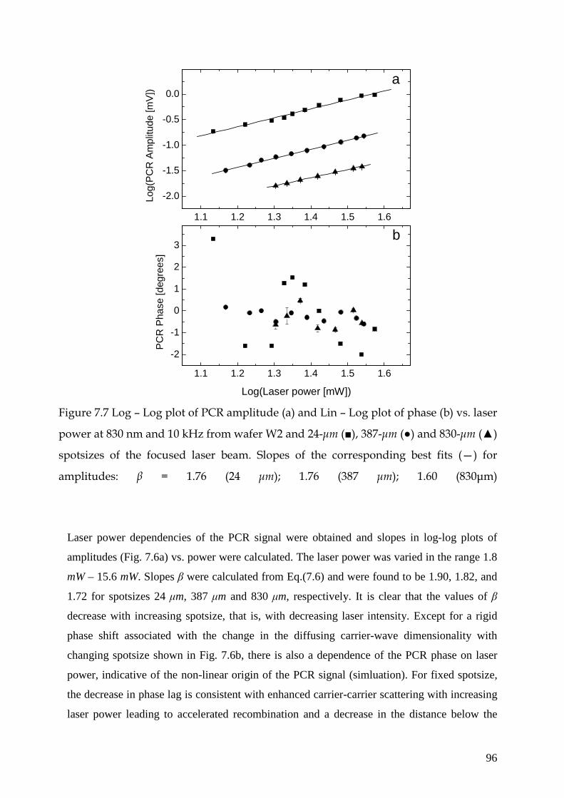
96
1.1 1.2 1.3 1.4 1.5 1.6
-2.0
-1.5
-1.0
-0.5
0.0
1.1 1.2 1.3 1.4 1.5 1.6
-2
-1
0
1
2
3
a
Log(
PC
R A
mpl
itude
[mV
])
b
PC
R P
hase
[deg
rees
]
Log(Laser power [mW])
Figure 7.7 Log – Log plot of PCR amplitude (a) and Lin – Log plot of phase (b) vs. laser
power at 830 nm and 10 kHz from wafer W2 and 24-µm (), 387-µm () and 830-µm ()
spotsizes of the focused laser beam. Slopes of the corresponding best fits (—) for
amplitudes: β = 1.76 (24 µm); 1.76 (387 µm); 1.60 (830µm)
Laser power dependencies of the PCR signal were obtained and slopes in log-log plots of
amplitudes (Fig. 7.6a) vs. power were calculated. The laser power was varied in the range 1.8
mW – 15.6 mW. Slopes β were calculated from Eq.(7.6) and were found to be 1.90, 1.82, and
1.72 for spotsizes 24 µm, 387 µm and 830 µm, respectively. It is clear that the values of β
decrease with increasing spotsize, that is, with decreasing laser intensity. Except for a rigid
phase shift associated with the change in the diffusing carrier-wave dimensionality with
changing spotsize shown in Fig. 7.6b, there is also a dependence of the PCR phase on laser
power, indicative of the non-linear origin of the PCR signal (simluation). For fixed spotsize,
the decrease in phase lag is consistent with enhanced carrier-carrier scattering with increasing
laser power leading to accelerated recombination and a decrease in the distance below the

97
wafer surface of the location of the carrier density wave centroid, physically a diffusion-
limited free carrier mean free path [Mandelis, 2001]. Decreasing the spotsize affects the
dimensionality of the diffuse carrier density wave, enhancing the radial diffusion degrees of
freedom and shifting the carrier-wave centroid phase lag farther away from surface. The
experimental results of the optical power dependence for the W2 are shown in Fig. 7.7.The
laser power was varied in the range 13.6 mW – 37.5 mW and, again, the slopes β were found
to decrease with decreasing intensities. Furthermore, they were consistently lower than those
measured with the long-lifetime wafer W1. There was no measurable phase shift with laser
spotsize or power changes in Fig. 7.7(b). This behavior at the considered frequency
(f=10kHz) may be the result of a weaker non-linearity mechanism sample W2 than in W1, as
expected from the shorter lifetime and smaller photogenerated root mean square rms free-
carrier-density in the former Si wafer.
Another set of measurements was made at the High Resolution PCR System using the
highly focused set-up shown in Fig. 7.3 at 10 kHz. Figure 7.8(a) shows the power dependence
of PCR amplitude for wafer W1 in the range 6 mW – 25 mW. The slope was found to be 1.89.
The phase lag exhibited a slight decrease with increasing laser power, Fig. 7.8(b), as expected
from enhanced carrier scattering processes. The same measurement was repeated with wafer
W2 and the results are shown in Fig. 7.9

98
0.7 0.8 0.9 1.0 1.1 1.2 1.3 1.4 1.5
-4.0
-3.8
-3.6
-3.4
-3.2
-3.0
-2.8
-2.6
0.8 0.9 1.0 1.1 1.2 1.3 1.4
-23.0
-22.5
-22.0
-21.5
-21.0
a
Log(
PC
R A
mpl
itude
[mV
])
b
PC
R P
hase
[deg
rees
]
Log(Laser power [mW])
Figure 7.8 Log – Log plot of PCR amplitude (a) and Lin – Log plot of phase (b) vs.
laser power () at 532 nm and 10 kHz from wafer M 28 and 18-µm spotsize of the
focused laser beam. Slope of the corresponding best fit (—) for amplitude: β = 1.89
(18 µm).

99
0.09 0.10 0.11 0.12 0.13 0.14
-4.00
-3.75
-3.50
-3.25
0.09 0.10 0.11 0.12 0.13 0.14
-4.9
-4.8
-4.7
-4.6
-4.5
-4.4 b
Log(
PC
R A
mpl
itude
[mV
])
a
PC
R P
hase
[deg
rees
]
Log(Laser power [mW])
Figure 7.9 Log – Log plot of PCR amplitude (a) and Lin – Log plot of phase (b) vs. laser
power () at 532 nm and 10 kHz from wafer W2 and 18-µm spotsize of the focused laser
beam. Slope of the corresponding best fit (—) for amplitude: β = 1.94 (18 µm).
Laser power was varied between 8.7 mW and 22.4 mW and the amplitude slope was 1.94. No
discernible PCR phase dependence on laser power was found. This result at 532 nm is
consistent with the 830-nm results obtained with this wafer. They can both be understood in
terms of the short recombination lifetime, which renders the subsurface position of the
diffusive carrier-wave density centroid [Mandelis, 2001] essentially independent of lifetime at
the frequency of these experiments. The higher slopes than those obtained at 830 nm are due
to the increased laser-induced carrier-wave densities as discussed below.

100
7.4.2. Modulation frequency dependence at the low resolution system.
Figure 7.10 shows frequency scans obtained from wafer W1 and three laser powers at a
spotsize of 830 nm. The corresponding best fits of the 3-D theory, Eq. (7.10) with β = 1 to the
data are also shown. The phases, Fig. 7.10(b) nearly overlap and thus they appear not to
depend strongly on laser power. Figure 7.6(b) shows a change of ~ 10 degrees between 1.8 –
15.6 mW at 10 kHz. Small differences on the order of 2° exist among phases across the
narrower power range in Fig. 7.10(b), however, they are nearly imperceptible over the full 75°
phase range. The frequency dependence of the PCR signals using the same laser powers and
24 µm and 387 µm spotsizes exhibited similar behavior.
0.1
1
10-2 10-1 100 101 102
-70
-60
-50
-40
-30
-20
-10
0
a
Log(
PC
R A
mpl
itude
[mV
])
b
PC
R P
hase
[deg
rees
]
Log (Frequency [kHz])

101
Figure 7.10 Experimental frequency scans (10 Hz – 100 kHz) of PCR amplitudes (a)
and phases (b) from wafer W1 for various 830-nm laser powers focused to an 830-µm
spotsize, and the corresponding multiparameter theoretical 3-D best fits (—) using
Eq. 7.10 with β = 1. Laser power: 20 mW (), 15.2 mW () and 9.6 mW ().
Figure 7.11 shows the frequency dependent PCR signals from wafer W1 using 20 mW and
various spotsizes, as well as the corresponding best fits to the 3-D theory, Eq. (7.10),
with β = 1. Figure 7.11(b) shows significant phase changes with spotsize at high frequencies
due to changes in the dimensionality of the PCR signal [Rodriguez et al., 2000].
1E-1
1
1E-2 1E-1 1 10 100-80
-70
-60
-50
-40
-30
-20
-10
0
a
Log(
PC
R A
mpl
itude
[mV
])
b
PC
R P
hase
[deg
rees
]
Log (Frequency [kHz])

102
Figure 7.11 Experimental frequency scans (10 Hz – 100 kHz) of PCR amplitudes (a)
and phases (b) from wafer W1 for 830-nm and 20 mW laser beam focused to various
spotsizes: 24 µm (), 387 µm () and 830 µm (). Best theoretical 3-D fits (—) using
Eq. 7.4 with β = 1 are also shown.
The results of best-fitting the 3-D theory to the data and extracting transport parameters are
shown in Table 7.1 The frequency dependencies of the PCR signals generated with laser
powers 15.2 mW and 9.6 mW and focused on the same spotsizes exhibited similar behaviors.
Table 7.1. Best-fitted computational results for sample W1. Experimental data at 830
nm 3-D theory and integer values of the non-linearity coefficient β
3-D Model, Eq. (7.10)
β = 1 β = 2
Power
P0 [mW]
Transport and Beam Parameters 24 µm 387 µm 830 µm 24 µm I0 [W/m2] 21.2×10⁶ 8.2×10⁴ 1.8×10⁴ 21.2×10⁶
∆N[1/cm3] 8. ×1018 9.51016 3.9×10¹⁶ 6.6×10¹⁷ τ [µs] 39.3 49.3 84.9 35.9
D [cm2/s] 0.31 4.2 9.9 11.1 S1 [cm/s] 0.07 980 960 4.3×10³
9.6
S2 [cm/s] 2.3×10⁴ 2.4×10⁴ 3.7×10³ 1.2×10⁴ I0 [W/m2] 33.6×10⁶ 1.3105 2.8×10⁴ 33.6×10⁶
∆N[1/cm3] 1.5×10¹⁹ 1.31017 4.3×10¹⁶ 9.6×10¹⁷ τ [µs] 43.5 42.6 55.1 28.8
D [cm2/s] 0.26 4.9 5.5 9.9 S1 [cm/s] 62 890 787 4×10³
15.2
S2 [cm/s] 4.4×10³ 4×10³ 6.8×10³ 1.2×10⁴ I0 [W/m2] 44.2×10⁶ 1.7×10⁵ 3.7×10⁴ 44.2×10⁶
∆N[1/cm3] 1.7×10¹⁹ 1.7×10¹⁷ 5.4×10¹⁶ 1.2×10¹⁸ τ [µs] 37.2 43.8 51.6 26.7
D [cm2/s] 0.26 5.3 4.7 10 S1 [cm/s] 60 890 740 4×10³
20
S2 [cm/s] 1.7×10⁴ 6.5×10³ 3.6×10⁴ 1.2×10⁴
The theoretical best fits in Figs. 7.10 and 7.11 were made using a computational program
which minimizes the variance of the combined amplitude and phase fits [Li et al., 2005].
Furthermore, the PCR signals were fitted using a non-linear extension of the foregoing 3-D
computation algorithm with β = 2. It is important to recall that fractional powers 1 < β < 2

103
could not be efficiently accommodated in the 3-D PCR theory, Eq. (7.10). A 1-D non-linear
best-fit algorithm was generated based on Eq. (7.9) and capable of accommodating arbitrary
values 1 ≤ β ≤ 2. The computational algorithm was implemented with the corresponding
experimental values for β (Fig. 7.6 for sample W1) and numerical quantities are presented in
Table 7.2.
Table 7.2. Best-fitted computational results for sample W1. Experimental data at 830
nm 1-D theory and experimental values of non-linearity coefficient β.
1-D Model, Eq. (7.9)
β = 1.82 β = 1.72
Power
P0 [mW]
Transport and Beam Parameters
387 µm 830 µm I0 [W/m2] 8.2×10⁴ 1.8×10⁴
∆N[1/cm3] 4×10¹⁶ 3.2×10¹⁶ τ [µs] 31.1 81.4
D [cm2/s] 25 28.7 S1 [cm/s] 1×10⁴ 7×10³
9.6
S2 [cm/s] 420 9.1×10³ I0 [W/m2] 1.3105 2.8×10⁴
∆N[1/cm3] 7.4×10¹⁶ 4.1×10¹⁶ τ [µs] 27.9 65.8
D [cm2/s] 9.2 27.5 S1 [cm/s] 4.8×10⁴ 6.9×10³
15.2
S2 [cm/s] 0.3 9.7×10³ I0 [W/m2] 1.7×10⁵ 3.7×10⁴
∆N[1/cm3] 8.7×10¹⁶ 5×10¹⁶ τ [µs] 28 59.8
D [cm2/s] 15.3 24.7 S1 [cm/s] 1.1×10⁴ 6.5×10³
20
S2 [cm/s] 0.2 9.9×10³
In all tables the photogenerated excess carrier-wave densities (m-3) shown are mean values
calculated using the expression:

104
∆Ν =( )
019 2
0
1
21.6 10 ( ) [ ( ) ] 1/D P
P
W L f
τω π α−
× + h
, (7.11a)
where P0 is the incident power [W]; 0ωh is the incident photon energy expressed in eV
,ω0 = hc/λP is the photon angular frequency at the wavelength of the laser; and αP is the
optical absorption coefficient at the excitation wavelength. LD(f) is the magnitude of the
complex carrier diffusion length ( )1 2
D
DL f
i f
τπ τ
=+
. (7.11b)
Values of LD and τ used in Eq. (7.11) were calculated from the multiparameter best-fit values
obtained from Tables 7.1-7.4. From Table 7.1 the values of lifetimes obtained with the linear
3-D theory, β = 1, and 24-µm spotsize, are reasonable for p-Si [Rodriguez et al., 2000],
however, the corresponding diffusion coefficients are outside the typical range for p-type
wafers [Rodriguez et al., 2000]. Table 7.1 also shows the results of the same experimental
data, Figs. 7.8 and 7.9, fitted with the 3-D theory and β = 2, Eq. (7.10). The experimental
slope for 24 µm laser spotsize (β = 1.9) is very close to 2 and validates this fitting procedure.
Fitting error was very low, 0.6% – 0.9%. The measured transport parameters for all laser
intensities and 24 µm spotsize can be compared for β = 1 and β = 2 from Table 7.1. It is seen
that recombination lifetimes consistently decrease in the non-linear fit. This decrease is larger
for higher intensities reaching up to 43%. The absolute value of the lifetime monotonically
decreases with increasing intensity for β = 2, as expected from the increased carrier-wave
densities and the proportionately increased scattering probabilities which limit the diffusion
length (or mean free path). In the non-linear fit, carrier diffusivity values increase
dramatically from unrealistically low levels at β = 1: They rise to values approx. 10 cm2/s,
which is normal medium to high injection conditions (∆N ~ 1018 – 1019 cm-3). Front surface
recombination velocities also increase considerably in the non-linear fit, and remain
essentially unchanged with increasing intensity, as expected, since the defect / recombination
center density on the surface is not affected by the incident photon flux. Back surface
recombination velocities do not change as dramatically under the non-linear fit. They are
higher than S1, as expected from the matte nature of the back surfaces of our wafers compared
to the polished front surfaces. No attempt for non-linear fits to the data corresponding to 387
µm and 830 µm spotsizes was made, as the slopes (β = 1.82 and 1.72) were far from β = 2 to
guarantee the validity of the 3-D computation. As shown in Fig. 3.8, the best fits of PCR
signals generated with the relatively large spotsizes, 2W ~ 830 µm , yield very similar sets of

105
transport parameters using either 1-D or 3-D linear theories (β = 1) only when τ < 20 µs. This
is not the case with sample W1 as seen in Table 7.2. However, for comparison with Table 7.2,
the β = 1 parameters were calculated using the 3-D theory and are shown in Table 7.1. Table
7.2 shows results from PCR signals with 2W = 387 µm and 830 µm fitted to the non-linear 1-
D theory, Eq. (12), with β = 1.82 and 1.72, from Fig. 7.6(a). In view of Fig. 3.7 and the best-
fitted values of recombination lifetime under all excitation intensities, the calculated transport
parameters with the 1-D model can only be considered to be approximate. The excess
photoinjected carrier densities are somewhat lower than the 2W = 24-µm case. Recombination
lifetimes under all incident intensities do not change much from the β = 1 values but they
decrease monotonically with increased intensity, as expected for enhanced carrier-carrier
scattering [Li et al.,1997]. It is noted that the lifetime obtained under 9.6 mW excitation and
2W = 830 µm is 81.4 µs, close to the value 84.9 µs obtained from fitting the same data with
the 3-D theory and β = 1. These differences increase with increasing incident intensity. As
observed with 2W = 24 µm spotsize, for non-linear fits with β = 1.82 (2W = 387 µm) and β =
1.72 (2W = 830 µm) the values of D increased manifold over the β = 1 values, attaining the
normal range of p-Si [Rodriguez et al., 2000]. However, the values of D are larger than those
obtained with 2W = 24 µm as expected from the much lower intensities accompanying the
larger spotsizes. Only slight decreases are observed with increasing intensity [Li et al.,1997].
Front and back surface recombination velocities do not undergo significant changes for all
non-linear fits, β = 2 (2W = 24 µm), β = 1.82 (2W = 387 µm) and β = 1.72 (2W = 830 µm).
This is as expected from the intrinsic defect structure of the wafer surfaces. S2 is consistently
higher than S1 for all incident intensities. The comparison between Tables 7.1 and 7.2 show
that the difference between the β = 1 values and the non-linear results is large and due to the
non-linearity exponents β = 1.72 and 1.82. This comparison demonstrates the need for precise
knowledge of the degree of non-linearity of the PCR signal in order to obtain physically
reasonable and reliable (i.e. self-consistent) measurements of semiconductor transport
properties. Figure 7.12 shows two sets of modulation frequency scans obtained from wafer
W2 including the corresponding best fits to 3-D theory with β = 1. The phase plots at fixed
spotsize nearly overlap, Fig. 7.12b, and are essentially independent of laser power, consistent
with Fig. 7.7b. Figure 7.13 shows frequency scans with 38-mW laser power and various
spotsizes. The corresponding 3-D theoretical best fits to Eq. (7.10) and β = 1 are also shown.

106
9E-31E-2
2E-2
3E-2
4E-2
5E-2
1 10 100
-25
-20
-15
-10
-5
0
5
a
Log(
PC
R A
mpl
itude
[mV
])
b
PC
R P
hase
[deg
rees
]
Log (Frequency [kHz])
Figure 7.12 Experimental frequency scans (500 Hz – 100 kHz) of PCR amplitudes (a)
and phases (b) from wafer W2 for various 830-nm laser powers focused to an 830-µm
spotsize and the corresponding theoretical 3-D best fits (—) using Eq. 7.4 with β = 1.
Laser power: 38 mW () and 12 mW ().

107
1E-1
1
1 10 100
-25
-20
-15
-10
-5
0
a
Log(
PC
R A
mpl
itude
[mV
])
b
PC
R P
hase
[deg
rees
]
Log (Frequency [kHz])
Figure 7.13 Experimental frequency scans (500 Hz – 100 kHz) of PCR amplitudes (a)
and phases (b) from wafer W2 for 830-nm, 38 mW laser beam focused to various
spotsizes: 24 µm (), 387 µm () and 830 µm (). Best theoretical 3-D fits (—) using
Eq. 7.4 with β = 1 are also shown.
The phase shifts at the high-frequency end of Fig. 7.13b are due to changing signal
dimensionality from 3-D (2W = 24 µm) to 1-D (2W = 830 µm). The frequency dependence of
the PCR signals with excitation power 12 mW and the same spotsizes exhibited similar
behavior. The PCR signals of Fig. 7.12 were fitted to 1-D theory using the actual
experimental non-linear values for β, Fig. 7.7a. Calculated transport parameters are presented
in Table 7.3.

108
Table 7.3. Best -fitted computational results for sample W2. Experimental data at 830
nm with 1-D and 3-D theories, linear and various non-linearity coefficients
3-D Fitting Model 1-D Fitting Model
β = 1 β = 1.76 β = 1.60
Power P0
[mW]
Transport and Beam Parameters 387 µm 830 µm 387 µm 830 µm I0 [W/m2] 1×10⁵ 2.2×10⁴ 1×10⁵ 2.2×10⁴
∆N[1/cm3] 3.6×10¹⁵ 6.2×10¹⁴ 1.6×10¹⁵ 3.9×10¹⁴ τ [µs] 1.3 0.9 0.54 0.55
D [cm2/s] 24.6 34.5 23.2 23.4 S1 [cm/s] 9.3×10³ 370 390 390
12
S2 [cm/s] 3.9×10⁴ 2.2×10⁴ 1.6×10⁴ 1.6×10⁴ I0 [W/m2] 3.2×10⁵ 7×10⁴ 3.2×10⁵ 7×10⁴
∆N[1/cm3] 1×10¹⁶ 2.2×10¹⁵ 4.8×10¹⁵ 1.5×10¹⁵ τ [µs] 1.3 1.1 0.51 0.65
D [cm2/s] 32 32.2 23.4 19.5 S1 [cm/s] 8×10³ 430 407 920
38
S2 [cm/s] 1.5×10⁴ 2.4×10⁴ 1.5×10⁴ 1.6×10⁴
Unlike sample W1, the short-lifetime (τ ∼ 1 µs) wafer W2 did yield PCR frequency scans
which could be considered fully one-dimensional under the expanded laser beam spotsizes of
387 and 830 µm, as the numerical simulations of PCR signal presented on Fig. 4.9. At 2W =
24 µm the supra-linear slope β = 1.76, Fig. 7.7a, did not allow using the 3-D Eq. (7.10) to fit
the data and yield representative values of the transport parameters since we could only use
integer values of β. Therefore, only fits for the largest two spotsizes are shown in Table 7.3.
Here the lifetimes are very short for both linear and non-linear fits and they do not change
perceptively with increased laser intensity. This fact may be traced to the relatively low
photoexcited carrier-wave densities in the 1014 – 1015 cm-3 range, using Eq. (7.11). These are
up to four orders of magnitude lower than those estimated for the sample W1. The best-fitted
diffusivities are in the range of acceptable values for p-Si [Rodriguez et al., 2000] and vary
little with increased intensity; again, owing to the relatively low ∆Ν. Front-surface
recombination velocities are lower than back-surface velocities, as expected. There are large
differences between the linear and non-linear fits for the same W which lead to the same
conclusion as in the case of wafer W1 in terms of the importance of using the actual non-
linear exponent obtained experimentally in order to calculate the transport parameters. In
summary, there were neither large differences in values of the transport parameters between

109
excitation with 12 and 38 mW, nor were clear trends in those parameters established. This
would be expected under low-injection conditions, however, in these experiments the ∆Ν
range corresponded to intermediate conditions [Bullis and Huff, 1996].
7.4.3. Modulation frequency dependence at 532 nm
Figures 7.14 and 7.15 show the frequency dependent amplitude and phase of the PCR
signal from wafers W1 and W2, respectively, using several laser powers and 18 µm spotsize.
The corresponding best fits to the 3-D theory, Eq. (7.10), are also shown.
1E-4
1E-3
1E-2 1E-1 1 10 100
-40
-30
-20
-10
0
a
Log(
PC
R A
mpl
itude
[mV
])
b
PC
R P
hase
[deg
rees
]
Log (Frequency [kHz])
Figure 7.14 Experimental frequency scans (10 Hz – 100 kHz) of PCR amplitudes (a)
and phases (b) from wafer W1 for various 532-nm laser powers focused to an 18-µm
spotsize and the corresponding theoretical 3-D best fits (—) using Eq. 7.4 with β = 2.
Laser power: 16 mW (), 13.2 mW () and 9.6 mW ().
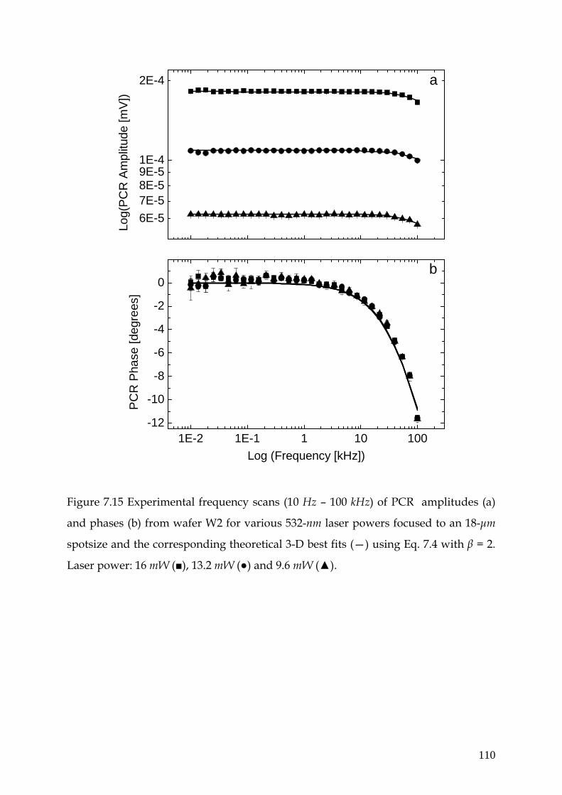
110
6E-5
7E-58E-59E-51E-4
2E-4
1E-2 1E-1 1 10 100-12
-10
-8
-6
-4
-2
0
a
Log(
PC
R A
mpl
itude
[mV
])
b
PC
R P
hase
[deg
rees
]
Log (Frequency [kHz])
Figure 7.15 Experimental frequency scans (10 Hz – 100 kHz) of PCR amplitudes (a)
and phases (b) from wafer W2 for various 532-nm laser powers focused to an 18-µm
spotsize and the corresponding theoretical 3-D best fits (—) using Eq. 7.4 with β = 2.
Laser power: 16 mW (), 13.2 mW () and 9.6 mW ().

111
While the amplitudes scale non-linearly with laser power with slopes β = 1.89 (W1, Fig. 7.8)
and β = 1.94 (W2, Fig.7.7), the phases at the various laser powers nearly overlap, consistently
with Figs. 7.8b and 7.7b. The best fits to Eq. (7.10) presented in Figs. 7.14a and 7.15a were
made using β = 2. This value of β is very close to the experimentally measured slopes,
therefore it is expected that transport parameters obtained from these fits are close to those
that would have been obtained using the exact experimental supra-linear slopes. The
multiparameter best-fit results to the data are presented in Table 7.4 for three laser powers.
Table 7.4. Best-fitted computational results for samples W1 and W2. Experimental
data at 532 nm with 3-D theory.
3-D Fitting Model for Wafer W1
3-D Fitting Model for Wafer W2
Power P0
[mW]
Transport and Beam Parameters Β = 1 β = 2 β = 1 β = 2 I0 [W/m2] 3.8×10⁷ 3.8×10⁷ 3.8×10⁷ 3.8×10⁷ ∆N[1/cm3] 3.6×10²⁰ 3.1×10¹⁹ 3×10¹⁸ 8.3×10¹⁷ τ [µs] 238 70.5 4.2 0.34
D [cm2/s] 0.46 2.7 5.7 8.9 S1 [cm/s] 123 5.6×10⁴ 6.7×10³ 3.7×10³
9.6
S2 [cm/s] 2×10⁴ 9.4×10⁴ 4.2×10⁴ 9.8×10³ I0 [W/m2] 5.2×10⁷ 5.2×10⁷ 5.2×10⁷ 5.2×10⁷ ∆N[1/cm3] 6.1×10²⁰ 3.4×10¹⁹ 4.4×10¹⁸ 1.2×10¹⁸ τ [µs] 259 56.7 3.5 0.34
D [cm2/s] 0.37 2.9 4.7 8.9 S1 [cm/s] 184 4.3×10⁴ 6.3×10³ 3.7×10³
13.2
S2 [cm/s] 4.3×10⁴ 8.6×10⁴ 3.7×10⁴ 9.9×10³ I0 [W/m2] 6.3×10⁷ 6.3×10⁷ 6.3×10⁷ 6.3×10⁷ ∆N[1/cm3] 5.9×10²⁰ 3×10¹⁹ 5.5×10¹⁸ 1.6×10¹⁸ τ [µs] 200 44.5 4.1 0.33
D [cm2/s] 0.35 3.2 4.8 6.2 S1 [cm/s] 241 4×10⁴ 7.4×10³ 3.6×10³
16
S2 [cm/s] 3.9×10⁴ 6.8×10⁴ 6.9×10⁴ 9.6×10³
For sample W1 the values of τ decrease with increasing laser intensity, in a manner similar to
that observed with 830-nm irradiation, Table 7.1. The relative values of τ for excitation with
beam spotsizes 18 and 24 µm at the two distinct wavelengths, Tables 7.1 and 7.4, are quite
close, within a factor of two. On the other hand, in Table 7.4 the values of τ obtained with β =
2 for the three incident intensities I0, are more than three times smaller than those obtained

112
with β = 1. Once again, this shows the dramatic difference the non-linearity coefficient value
can make in PCR measurements. The diffusion coefficients obtained using β = 1 are far from
the range of acceptable values for this parameter for p-type wafers [Rodriguez et al., 2000]
and those obtained with β = 2 are marginally within the range of typical values. This is
approx. one order of magnitude smaller than the D values obtained in Table 7.1 and is
probably due to the much stronger carrier-carrier scattering at high-injection carrier-wave
densities in the 1019 – 1020 cm-3 range [Li et al., 1997]. The best-fitted values of S1 obtained
with β = 1 are more than 100 times lower than those obtained with β = 2. The latter values are
essentially independent of laser intensity (also the case in Table 7.1 under 830-nm excitation)
but are clearly higher than their β = 2 counterparts in Table 7.1. This, along with differences
in τ (532 nm) and τ (830 nm), is expected, because the optical absorption depth at 523 nm is
much shorter (0.96 µm; αP = 10,340 cm-1) than that at 830 nm (15.2 µm; αP = 658.9 cm-1)
with the consequence that optical injection samples the defect densities in the near-surface
region must more strongly at 523 nm than at 830 nm, thus exhibiting enhanced sensitivity to
surface recombination and yielding a larger effective surface recombination velocity S1. The
back-surface recombination velocities are all in the range of 104 cm/s for both wavelengths,
Tables 7.1 and 7.4. Physically, they should be the same, however our simulations show that
the shallower optical penetration depth at 523 nm renders the PCR signal less sensitive to S2
than that at 830 nm. The best fits to Eq. (7.10) resulting from the W2-sample experimental
data with β = 1 and 2 are also shown in Table 7.4. The values of τ obtained with β = 2 which
is very close to the experimental value β = 1.94 for all laser powers are in the sub-µs range,
consistently with those obtained at 830 nm in Table 7.2. In fact, they are approx. two times
smaller under 523-nm excitation as expected from a significantly higher intensity range
(about three orders of magnitude) and the corresponding high-injection ramifications. The τ
values obtained with the linear fit are very unrealistic in comparison with other data in Table
7.4, more than ten times larger than those obtained with β = 2. The carrier diffusivity values in
Table 7.4 are considerably smaller than those in Table 7.2 and decrease with increased power
16 mW. These trends are consistent with the shallower penetration depth, higher photoinjected
carrier-wave densities and higher laser intensities under 523 nm excitation [Li et al., 1997]. In
a manner similar to the behavior of sample W1, the S1 values under 523-nm excitation are
higher than under 830-nm, whereas values of S2 are very close. Overall, values of the
transport parameters in Table 7.4 fitted with β = 1 show some significant deviations from the
non-linear fits, especially for τ and S1.

113
7.5 Summary
It is interesting to note for both samples that the ca has three-orders-of-magnitude
higher intensities and shorter optical absorption depth at 523 nm which are associated with
increased non-linearity exponents which tend to values closer to 2, a limiting value for
electron-hole band-to-band bipolar recombination [Guidotti et al, 1988-1989; Nuban and
Krawczyk, 1997; Nuban and Krawczyk, 1997]. In that limit, band-to-defect recombination
may be dominated by the N×P product of electron-hole density recombination. A different
mechanism for quadratic PL dependence on photo-carrier density may have to be considered
such as proposed by Guidotti et al. [Guidotti et al, 1988-1989] and Nuban et al. [Nuban and
Krawczyk, 1997; Nuban and Krawczyk, 1997] and which have been discussed in the context
of Eq. (3.1).

114
Chapter 8: Conclusion and outlook
This final chapter summarizes the main conclusions of this dissertation and outlines the
directions for the future research. Following the organization of the thesis the last chapter is
also devided into two parts. The first section is concerned with the thermal properties of
Cd1-xMgxSe single crystals, the second one is devoted to the new developed technique of
photocarrier radiometry (PCR).
Thermal properties of Cd1-xMgxSe single crystals
Pyroelectric experiments have proven to be a valuable tool to characterize the thermal
parameters of Cd1-xMgxSe single crystals in a limited temperature range around room
temperature. With a home-made apparatus the thermal diffusivity of Cd1-xMgxSe single
crystals could be determined experimentally. It was shown on the glassy carbon (reference
sample) that the thermal diffusivity can be determined directly from measured PPE
amplitudes and phases when sample and detector are thermally thick and optically opaque.
From these data the thermal conductivity of these compounds was estimated. It was found that
thermal conductivity of Cd1-xMgxSe single crystals decreases by a factor of three as the Mg
concentration is increased from zero to about 50 %. This strong variation could be explained
by structural effects of the mixed crystal.
Future work should concentrate on development of the photopyroelectric cell able to
measure in broader temperature range. From the theoretical point of view it is very interesting
to develop theoretical model for mixed crystals to elucidate the relative role of the electronic
and phonon contributions to thermal conduction and the mass-scattering effects as well.

115
Photocarrier radiometry signal
It was shown that in some cases the existence of a space charge layer or bipolar
recombination mechanism can be important when the electrical transport properties of a
silicon wafers are measured by photocarrier radiometry (PCR).
In chapter 6 the interface modulated-charge-density theory developed by Mandelis
[Mandelis, 2005a] was experimentally proved. The interface modulated-charge-density theory
developed by Mandelis [Mandelis, 2005a] was used for physical simulations involving PCR
signals in order to study the effects of the various SCL optoelectronic transport parameters on
the PCR amplitude and phase signal channels. Furthermore, an experimental configuration
was used involving n- and p-doped Si – SiO2 interfaces and a low-intensity (non-perturbing)
modulated laser source as well as a co-incident dc laser of variable intensity acting as
interface-state neutralizing optical bias. The application of the theory to the experiments
yielded the various transport parameters of the samples as well as the depth profile of the
SCL. It was shown that PCR can monitor the complete flattening of the energy bands at the
interface of p-Si – SiO2 with dc optical powers up to a 300 mW. The uncompensated charge
density at the interface was also calculated from the theory. It was found that this
methodology is the relatively low efficient for driving n-Si into the flatband state. The
independence of PCR phases from IDC is an additional indicator that the optical bias does not
affect the transport properties of the SiO2 - n-Si interface. This behavior was explained by the
much lower (ca. 100 times [Aberle, 1992]) minority carrier capture cross-section of the n-type
interface. This fact leads to much shorter interface lifetimes, τs [Mandelis, 2005a], making it
harder for an optical source to build up the neutralized interface charge coverage observed
with p-Si – SiO2 interfaces, Fig. 6.15. The same effect makes the interface recombination
velocity essentially independent of excess carrier density at the n-Si – SiO2 interface [Aberle,
1992] which results in the independence of the PCR phase from PDC, Fig. 6.16.
In chapter 7 it was shown that the introduced nonlinear coefficient, which could be
determined from intensity-scans, can considerably improve estimated values of the carrier
transport parameters. It is interesting to note for both samples that the ca. has three-orders-
of-magnitude higher intensities and shorter optical absorption depth at 523 nm which are
associated with increased non-linearity exponents which tend to values closer to 2, a limiting
value for electron-hole band-to-band bipolar recombination [Guidotti et al, 1988-1989; Nuban
and Krawczyk, 1997; Nuban and Krawczyk, 1997]. In that limit, band-to-defect

116
recombination may be dominated by the N×P product of electron-hole density recombination.
A different mechanism for quadratic PL dependence on photo-carrier density may have to be
considered such as proposed by Guidotti et al. [Guidotti et al, 1988-1989] and Nuban et al.
[Nuban and Krawczyk, 1997; Nuban and Krawczyk, 1997] and which have been discussed in
the context of Eq. (3.1).
Altogether it is demonstrated that the photocarrier radiometry technique is a powerful
tool for the investigation of electronic properties of silicon wafers. The results of this work
show that a careful search has to take into account the influence of different experimental
conditions. Future work should be concentrate on developing 3 D photocarrier radiometry
signal theory extended for discussed phenomena in this work. Additional for ion implanted
wafers (such as presented in Section 4.1.7) the 3 D photocarrier radiometry signal theory in
layered sample developed by Li eat al. [Li, 2004] should be extended to take into account
phenomena related with a space charge layer and bipolar recombination mechanism.

117
Bibliography
[Abeles, 1963] B. Abeles, Phys. Rev. 131, 1906 (1963)
[Aberle et al.,1992] A. G. Aberle, S. Glunz and W. Warta, J. Appl. Phys. 71, 4422 (1992).
[Aberle et al., 1996] A. G. Aberle, J. Schmidt and R. Brendel, J. Appl. Phys. 79, 1491 (1996).
[Adachi, 1983] S. Adachi, J. Appl. Phys. 54, 1844 (1983)
[Almond and Patel, 1996] Almond, D. P. and Patel, P. M. (1996). Photothermal Science and
Techniques. Chapman & Hall, London.
[Angstrm, 1861] Angstrm, A. J. (1861). Ann. Physik. Lpz., 114:513.
[Augustine et al., 1992] G.Augustine, A. Rohatsi, N.M.Jokerst, Based doping optimization for
radiation-hard Si,GaAs and InP solar cells.,IEEE Trans. Electron Dev., 39:2395-2400, 1992
ASTM Standard F723-88, 1996 Annual Book of ASTM Standards, Am. Soc. Test. Mat., West
Conshohocken, PA (1996).
[Balageas et al. 1986] D. Balageas, J.C. Krapez, P. Cielo, J.Appl. Phys. 59,348-357
[Bandiera et al., 1982] Bandiera I.N., Closs, H. and Ghizoni, C.C. J. Photoacoust. 1982, 1,
275
[Bell, 1880] Bell, A. G. (1880), Upon the production of sound by radiant energy. Am.J. Sci.,
20, 305:324.
[Bhandari and Rowe, 1998] C. M. Bhandari, D. M. Rowe, Thermal Conduction in
Semiconductors, 1st edn. (Wiley Eastern Limited, New Delhi, 1998), pp. 59-77
[Boccara et al., 1980] Boccara, A. C., Fournier, D., and Badoz, J. (1980). Thermooptical
spectroscopy - detection by the 'mirage effect'. Appl. Phys. Lett., 36, 130:132.
[Bullis and H.R.Huff, 1996] W.M. Bullis and H.R.Huff, Interpretation of carrier
recombination lifetime and diffusion measurements in silicon, J.Electrochem Soc.,vol.143,
No.4, April 1996
[Carslaw and Jaeger, 1959] Carslaw, H. S. and Jaeger, J. C. (1959). Conduction of heat
in solids. Oxford University Press, 2nd edition
[Chirtoc and Mihailescu, 1989] M. Chirtoc, G. Mihailescu, Phys. Rev. B, 40, 9606 (1989)
[Delenclos et al, 2001] S. Delenclos, M. Chirtoc, A. Hadj Sahraoui, C. Kolinsky, J. M.
Buisine, Anal. Sci. 17, 161 (2001)
[Dietzel, 2001] Dietzel, D. (2001). Photothermische Mikroskopie an Ionenstrahl-
strukturierten Halbleitern und Halbleiterbauelementen. PhD thesis, Ruhr University Bochum.

118
[Dietzel et al., 2003a] Dietzel, D., Chotikaprakhan, S., Filip, X., Chirtoc, M., Bangert,H.,
Eisenmenger-Sittner, C., Neubauer, E., Pelzl, J., and Bein, B. K. (2003a). Cu-coatings on
carbon-Effects of plasma processing analysed by means of thermoreflectance microscopy. In
SFV, France, editor, Proceedings of 14th International Colloquium on Plasma Processes,
CIP'2003, pages 264-66, Antibes-Juan-les-Prins, France.
[Dziewoir and Schmid, 1977] J.Dziewor and W. Schmid, Auger coefficients for highly doped
and highly excited silicon, Appl. Phys. Lett. 31: 346-348, 1977
[Flashir and Cahen, 1986] H.Flashir and D.Cahen, IEEE Trans. UFFC, 1986, 13, 622
[Firszt et al.,1995] F.Firszt,H.Męczyńska, B.Sekulska, J.Szatkowski, W.Paszkowicz,
J.Kachniarz, Semicond. Sci. Technol. 10 (1995) 197-200.
[Firszt et al., 1996]. F. Firszt, S. Legowski, H. Męczyńska, H. Oczkowski, W. Osinska, J.
Szatkowski, W. Paszkowicz, Z. Spolnik, J. Cryst. Growth 159, 167 (1996)
[Firszt et al., 1998] F. Firszt, H. Męczyńska, B. Sekulska, J. Szatkowski, W. Paszkowicz, J.
Cryst. Growth 184/185, 1053 (1998)
[Fournier, 1992] Fournier, D. (1992). Competition between thermal and plasma waves for the
determination of electronic parameters in semiconductor samples. In Bicanic, D. and
Mandelis, A., editors, Photoacoustic and Photothermal Phenomena III, Springer Ser. Opt.
Sci., pages 339-348.
[Fotsing et al., 2003] Fotsing, J. L. N., Hoffmeyer, M., Chotikaprakhan, S., Dietzel, D., Pelzl,
J., and Bein, B. K. (2003). Laser modulated optical reflectance of thin semiconductor films on
glass. Rev. Sci. Instru., 74(1):873-876.
[Gerlach et al., 1972 ] W. Gerlach, H. Schlangenotto and H.Maeder, On the radaitive
recombination in silicon, Phys. Stat.Sol. A., 13:277-283, 1972
[Gruss et al., 1997] Gruss, C., Bein, B. K., and Pelzl, J. (1997). Measurement of high
temperatures by the probe beam reflection technique. High Temp. High Press., 29.
[Gou et al., 1997] Y. Gou, G. Aizin, Y. C. Chen, L. Zeng, A. Cavus, M. C. Tamargo, Appl.
Phys. Lett. 70, 1351 (1997)
[Guidotti et al, 1988] D. Guidotti, J. S. Batchelder, A. Finkel, and J. A. Van Vechten, Phys.
Rev. B, 38,1569 _1988;
[Guidotti et al., 1989] D. Guidotti, J. S. Batchelder, A. Finkel, P. D. Gerber, and J. A. Van
Vachten, J. Appl. Phys., 66, 2542 1989;
[Hall, 1952] R.N.Hall, Electron-hole recombination in germanium, Phys.Rev., 87:387, 1952
[Harren et al., 2000] Harren, F. J. M., Cotti, G., Oomens, J., and Hekkert, S. L. (2000).

119
Encyclopedia of Analytical Chemistry, chapter Photoacoustic spectroscopy in trace gas
monitoring, pages 2203-2226. John Wiley & Sons Ltd, Chichester.
[Haynes et al., 1956] J. R. Haynes and C. W. Westphal, Phys. Rev., 86, 647 _1956
[Holeman, 1972] B. R. Holeman, Infrared Phys. 12, 125 (1972)
[Ikari et al., 1999] T. Ikari, A. Salnick and A. Mandelis, J. Appl. Phys. 85, 7392 (1999).
[Quimby and Yen, 1980] R.S.Quimby, W.M.Yen, J.Appl.Phys, 1980, 51, 4985
[Ikari et al., 1999] T.Ikari, A.Salnick and A. Mandelis, Theoretical and experimental aspects
of three-dimensional infrared radiometry of semiconductors,J.Appl.Phys.85: 7292-7297, 1999
[Johnson, 1958] E. O. Johnson, Phys. Rev. 111, 153 (1958).[Krawczyk and Nuban, 1994]S.
K. Krawczyk and M. F. Nuban, Mater. Sci. Eng., B, 28, 452 1994.
[Kiepert et al., 1999] Kiepert, W., Obramski, H. J., Bolte, J., Brandt, K., Dietzel, D.,
Niebisch, F., and Bein, B. K. (1999). Plasma etching and ion implantation on silicon,
characterized by laser-modulated optical reflectance. Surf. Coat. Tech., 116:119:410-418.
[King and Hall, 1994] King O and Hall D G 1994-I Phys. Rev. B 50 10661
[Kitgawara, 1992] Y.Kitgawara, R.Hoshi, T.Takenada, J.Electrochem.Soc.,139:2277-
2281,1992
[Li et al.,1997] C. M. Li, T. Sjodin, and H. L. Dai, Phys. Rev. B, 56, 15252 _1997
[Li et al., 2004] D.Li, D.Shaughnessy, A.Mandelis and J.Batista, J.of Appl. Physics, Vol.95,
12: 7832-7840, 2004
[Li et al., 2005] B. Li, D. Shaughnessy, and A. Mandelis, J. Appl. Phys., 97, 023701 _2005
[Mandelis, 1998] A.Mandelis, Solid State Electronics, Vol.42, No.1., pp.1-15, 1998
[Mandelis and Zver, 1985] A.Mandelis and M.Zver, J.Appl.Phys. 57 (9), 1985, 4421-4430
[Mandelis, 1996] A.Mandelis, R.E.Wagner, Jpn. J.Appl.Phys., Part 1, 35, 1786 (1996)
[Mandelis et al, 1999] A.Mandelis, A.Salnick, L.Chen, J.Opsal, A.Rosencwaig, J.Appl. Phys.
85, 1811 (1999)
[Mandelis, 2000] A.Mandelis, Diffusion Waves and their uses, Physics Today, August 2000,
pages 29-34
[Mandelis, 2001]A. Mandelis, Diffusion-Wave Fields: Mathematical Methods and Green
Functions, Springer, New York _2001.
[Mandelis et al., 2003] A. Mandelis, J. Batista and D. Shaughnessy, "Infrared photo-carrier
radiometry of semiconductors: Physical principles, quantitative depth profilometry and
scanning imaging of deep sub-surface electronic defects", Phys. Rev. B 67, 205208-1-18
(May 2003)

120
[Mandelis, 2005a] A. Mandelis, “Theory of Space Charge Layer Dynamics at Oxide-
Semiconductor Interfaces under Optical Modulation and Detection by Laser Photocarrier
Radiometry”, J. Appl. Phys., 97, 083508-1 - 11 (April, 2005)
[Mandelis, 2005b] A. Mandelis, J. Batista, J. Gibkes, M. Pawlak and J. Pelzl, “Non-
Contacting Laser Photocarrier Radiometric Depth Profilometry of Harmonically Modulated
Band-Bending in the Space Charge Layer at Doped SiO2 – Si Interfaces”, J. Appl. Phys., 97,
083507-1 - 11 (April 2005)
[Marinelli 1992] M.Marinelli, U.Zammit, F.Mercuri, R.Pizzoferrato, J.Appl.Phys. 72 (3), 1
August 1992
[Meyer and Sigrist, 1990] Meyer, P. L. and Sigrist, M. W. (1990). Atmospheric pollution
monitoring using CO2-laser photoacoustic spectroscopy and other techniques.
Rev. Sci. Instru., 61(7):1779-1807
[Murphy and Aamont, 1977] Murphy, J. C. and Aamodt, L. (1977). Photoacoustic
spectroscopy of luminescent solids: Ruby. J. Appl. Phys., 48(8), 3502-3509.
[Nuban and Krawczyk, 1997] M. F. Nuban, S. K. Krawczyk, and N. Bejar, Mater. Sci. Eng.,
B, 44, 125 1997.
[Nordal and Kanstad, 1979] Nordal, E. and Kanstad, S. O. (1979) Photothermal radiometry.
Phys. Scripta, 20:659.
[Pelzl, 1984] J.Pelzl, In: Photoacoustic Effect, Braunschweig, pp.52-79
[Pelzl and Bein, 1990] J.Pelzl, and B.Bein, Photothermal chracterisation of plasma surface
modifications, Pure & Appl. Chem., 64 (5): 729-744, 1990
[Pelzl and Bein,1992] Pelzl, J. and Bein, B. K. (1992). Photothermal characterization of
plasma surface modications. Pure & Appl. Chem., 64(5):739-744.
[Perzynska et al., 2000] K. Perzynska, F. Firszt, S. Legowski, H. Meczynska, J. Szatkowski,
M. Biernacka, A. Gajlewicz, S. Tarasenko, P. Zaleski, J. Crys. Growth 214/215, 904 (2000)
[Philips et al., 1992] M. C. Philips, M. W. Wang, J. F. Swenberg, J. O. McCaldin, T. C. Mc
Gill, Appl. Phys. Lett. 61, 1962 (1992)
[Rombouts et al., 2005] M. Rombouts, L. Froyen, A. V. Gusarov, E. H. Bentfour, C.
Glorieux, J. App. Phys. 97, 24905 (2005)
[Rodriguez et al., 2000] M. E. Rodriguez, A. Mandelis, G. Pan, L. Nicolaides, J. A. Garcia,
and Y. Riopel, J. Electrochem. Soc., 147, 687 _2000.
[Rosencwaig and Gersho, 1976] Rosencwaig, A. and Gersho, A. (1976). Theory of the
photoacoustic effect in solids. J. Appl. Phys., 47:64-69.

121
[Rosencwaig et al., 1985] Rosencwaig, A., Opsal, J., Smith, W. L., andWillenborg, D. L.
(1985). Detection of thermal waves through optical re°ectance. Appl. Phys.Lett., 46(11):1013-
1015.
[Salazar, 2003] A. Salazar, Rev. of Sci. Instrum.,74, 825 (2003)
[Schaub, 2001] Schaub, E. (2001). New calibration procedure for absolute temperature
measurement on electronic devices by means of thermoreflectance technique. Anal. Sci., 17.
[ Schmidt and Aberle, 1997] J. Schmidt and A. G. Aberle, J. Appl. Phys. 81, 6186 1997.
[Schoefthaler et al., 1994] M. Schoefthaler, R. Brendel, G. Langguth and J. H. Werner, First
WCPEC (1994), p. 1509.
[Schroder, 1997] D. K. Schroder, IEEE Trans. Electron Dev. 44, 160 (1997).
[Schroder, 1998] D.K.Schroder, Semiconductor Material and Device Characterization,
chapter 7:439-448, Wiley, New York, 2nd edition, 1998
[Seidel, 1961] T. Seidel, Metallurgy of Elemental and Compound Semiconductors (Ed. R. O.
Grubel, Interscience, New York 1961).
[Shaughnessy, 2005] D.Shaughnessy, PhD thesis, University of Toronto, 2005
[Shockley and Read, 1952] W.Shockley and Jr.W.T.Read, Statistic of the recombination of
holes and electrons, Phys. Rev., 87:832-842, 1952
[Slack, 1972] G. Slack, Phys. Rev. B, 6, 3791 (1972)
[Smith, 1978] R.A. Smith, Semiconductors, Cambridge University Press, New York, 2nd
edition, 1978
[Sze, 1981] S. M. Sze, Physics of Semiconductor Devices, 2nd ed. Wiley, New York, 198l,
Chap. 7.2.
[Tritt, 2004] T.Tritt, Thermal conductivity: Theory, Properties and Applications, Kluwer
Academic, 2004[Tsen et al., 1997] K. T. Tsen, D. K. Ferry, A. Botchkarev, B. Sverdlov, A.
Salvador, H. Morkoc, Appl. Phys. Lett. 71, 1852 (1997)[Thielemann and Rheinlaender, 1985]
W. Thielemann and B.Rheinlaender, Solid State Electron, 1985, 28, 1111
[Wagner et al, 1996] R.E.Wagner, A.Mandelis, Semicond.Sci.Technol. 11, 300 (1996)
[Varshni, 1967] Y.P.Varshni, Band-to-band radiative recombination in groups IV,VI and III-
VI semiconductors (I), Phys. Stat.Sol., 19:459-514, 1967
[Zakrzewski, 2003] J.Zakrzewski, PhD thesis, Torun, Poland, 2003
[Tolev, 2007] J. Tolev, A. Mandelis and M. Pawlak, J. Electrochem. Soc. J. Electrochem.
Soc., Volume 154, Issue 11, pp. H983-H994 (2007)

122
[Tolev et al., 2008] On the non-linear dependence of photocarrier radiometry signals from Si
wafers on the intensity of the laser beam, J. Tolev, A. Mandelis and M. Pawlak, Eur. Phys. J.
Special Topics 153, 317-320 (2008)

123
Curriculum Vitae
PERSONAL DETAILS
Name Michał Janusz Pawlak
Nationality Polish
Date and place of birth 30.01.1978, Bydgoszcz, Poland
Address Moniuszki 5/3
87-100 Toruń
Poland
Contact [email protected]
tel.: +48 608 349 125
EMPLOYMENT HISTORY
Date Position
Since April 2009 IT specialist at Kujawsko-Pomorskie Voivodeship, Torun,
Poland
Nov 2008 – March 2009 Assistant at Ruhr University Bochum, Germany
Sept 2007 – April 2008 Postdoctoral Fellow at University of Toronto, Canada
May 2007 – August 2007 Assistant at Ruhr University Bochum, Germany
April 2004-March 2007 Scholarship holder at Ruhr University Bochum, Germany
Oct 2002 – March 2004 PhD student at Nicolaus Copernicus University, Torun,
Poland
Oct 2001 – June 2002 Assistant at Nicolaus Copernicus University, Torun, Poland

124
EDUCATION
Date Title Institution
April 2004-March 2007 Scholarship holder Ruhr University Bochum,
Germany
October 2002 – March 2004 PhD student Nicolaus Copernicus
University, Torun, Poland
Since April 2004 Electrical Eng. Warsaw University of
Technology, Poland
October 2000 – June 2002 Master of science
(Physics)
Nicolaus Copernicus
University, Torun, Poland
October 1997 – June 2000 Bachelor (Physics) Nicolaus Copernicus
University, Torun, Poland
PERSONAL QUALITIES
Programming in Java, Matlab, Labview; digital image processing, biomedical eng. Languages: Polish - native, English - good, German – basic.
125
List of publications and conference contributions
Publications
1. Photoacoustic Study of Zn1-x-yBexMnySe Mixed Crystals J. Zakrzewski, F. Firszt, S.
Łęgowski, H. Męczyńska, M. Pawlak, A. Marasek, abstract book 31st Winter School on
Molecular and Quantum Acoustics and 7th workshop on Photoacoustics and Photothermics,
page. 81, 2002.
2. Thermal Diffusivity Measurements of Zn1-x-yBexMnySe Mixed Crystals by Photoacoustic
Method J. Zakrzewski, F. Firszt, S. Łęgowski, H. Męczyńska, M. Pawlak, abstract book
28. Deutsche Jahrestagung fur Akustik, page 114, Bochum, 2002
3. Piezoelectric and pyroelectric study of Zn1-x-yBexMnySe mixed crystal, J. Zakrzewski, F.
Firszt, S. Legowski, H. Meczynska, M. Pawlak, and A. Marasek, Rev. of Scienfic
Instruments, vol. 74 nr 1, p. 566-568 (January 2003)
4. Photoacoustic investigation of Cd1-XMnXTe mixed crystals J. Zakrzewski, F. Firszt, S.
Łęgowski, H. Męczyńska, A. Marasek, and M. Pawlak, Rev. of Scienfic Instruments, vol.
74 nr 1, 572-574 (January 2003)
5. Photoacoustic Study of Cd1-x-yBexMnyTe Mixed Crystals, J. Zakrzewski, F. Firszt, S.
Łęgowski, H. Męczyńska, A. Marasek, M. Pawlak, Journal de Physic IV 109 (2003), 123-
126
6. Growth and characterization of selected wide – gap II – VI ternary solid solutions, F.
Firszt, S. Legowski, A.Marasek, H. Meczynska, M.Pawlak and J.Zakrzewski, abstract
book, International Symposium on 50th Anniversary of the Death of Prof. Dr. Jan
Chochralski, Torun, Poland, p. 4

126
7. Photoelectric and Photothermal Properties of Selected II – VI Compounds Mixed Crystals,
F. Firszt, S. Łęgowski, A. Marasek, H. Męczyńska, M. Pawlak and J. Zakrzewski, Opto-
electronics Rev. 12 (1), p. 161-164 (2004)
8. Study of optical properties of Zn1-xBexTe mixed crystals by means of combined modulated
IR radiometry and photoacoustics, M. Pawlak, J. Gibkes, J. L. Fotsing, J. Zakrzewski, M.
Mali ński, B. K. Bein, J. Pelzl, F. Firszt and A. Marasek,
J. Phys. IV France 117, p. 47-56 (2004)
9. Carrier - density - wave transport and local internal electric field measurements in biased
metal-oxide-semiconductor n-Si devices using contactless laser photo-carrier
radiometry,A.Mandelis, M.Pawlak, D.Shauhnessy, Semicond.Sci.Technol. 19, p. 1240-
1249 (2004)
10. Growth and Optical Characterization of Cd1-xBe xSe and Cd1-xMgxSe crystals,
F. Firszt, A. Wronkowska, A. Wronkowski, S. Łęgowski, A. Marasek,
H. Męczyńska, M. Pawlak, W. Paszkowicz, K. Strzałkowski, and J. Zakrzewski,
Cryst. Res. Technol. 40, No. 4/5, p. 386-394 (2005)
11. Piezoelectric photothermal study of Cd1-x-yBexZnySe crystals,J. Zakrzewski, F. Firszt,
S. Łęgowski, H. Męczyńska, A. Marasek, M. Pawlak, K. Strzałkowski, M. Maliński, and
L. Bychto, Journal de Physique IV 125, p. 473-476 (2005)
12. Photoacoustic Study of Cd1-XBeXSe Mixed Crystals, J.Zakrzewski, M.Pawlak, F. Firszt,
S. Łęgowski, A. Marasek, H. Męczyńska,M.Malinski , Int. Journal of Thermophysics 26
(1), p. 285 (2005)
13. Non – contacting Laser Photocarrier Radiometric Depth Profilometry Of Harmonically
Modulated Band – Bending In The Space Charge Layer At Doped SiO2 – Si Interfaces,
A.Mandelis, J. Batista, J.Gibkes ,M.Pawlak, J.Pelzl, Journal Of Applied Physics 97
083507 (2005).

127
14. Space charge layer dynamics at oxide-semiconductor interfaces under optical
modulation: Theory and experimentalstudies by non-contacr photocarrier radiometry, A.
Mandelis, J.Batista, J.Gibkes, J.Pelzl, J.Phys.IV France 125, 565-567 (2005)
15. Investigations of AII-BVI mixed crystals with the piezoelectric photothermal method,
M. Mali ński, L. Bychto, J. Zakrzewski, F. Firszt, M. Pawlak, P. Binnebesel,
Journal de Physique IV 125, p. 379-382 (2005)
16. Time-domain and lock-in rate-window photocarrier radiometric measurements of
recombination processes in silicon,A. Mandelis, M. Pawlak, Ch. Wang, I. Delgadillo-
Holtfort, J. Pelzl, Journal of Applied Physics 98, p.123518 (2005)
17. Photoacoustic and photothermal radiometry spectra of implanted Si wafers,
D.M.Todorovic, M. Pawlak, I. Delgadillo-Holtfort, J . Pelzl, European Physical Journal -
Special Topics 153,259-262 (2006).
18. Non-linear Dependence of Photocarrier Radiometry Signals from p-Si Wafers on Optical
Excitation Intensity, J. Tolev, A. Mandelis and M. Pawlak, J. Electrochem. Soc. J.
Electrochem. Soc., Volume 154, Issue 11, pp. H983-H994 (2007)
19. On the non-linear dependence of photocarrier radiometry signals from Si wafers on the
intensity of the laser beam, J. Tolev, A. Mandelis and M. Pawlak, Eur. Phys. J. Special
Topics 153, 317-320 (2008)
20. Laser Photothermal Radiometric Instrument For Industrial Steel Hardness Inspection, X.
Guo, K. Sivagurunathan, M. Pawlak, J. Garcia, A. Mandelis, S. Giunta, S. Milletari and
S. Bawa, conference material for 15th International Conference Of Photoacoustic And
Photothermal Phenomena in Leuven, Belgium, 2009 (July 2009)
21. Thermal Transport Properties of Cd1-xMgxSe Mixed Crystals Measured by Means of the
Photopyroelectric Method, M. Pawlak, F. Firszt, S. Łęgowski, H. Męczyńska, J. Gibkes
and J. Pelzl , Intern. Journal of Thermophysics 31, 1, 187-198 (2010)

128
Conference contributions
32nd Winter School on Molecular and Quantum Acoustics and 8th workshop on
Photoacoustics and Photothermics) w Szczyrku, Poland, (oral), 2003
Photoacoustic Study of Cd1-x-yBexMnyTe Mixed Crystals
International Symposium on 50th Anniversary of the Death of Prof. Dr. Jan Chochralski,
2003, Torun, Poland (2 posters), 2003
Growth and characterization of selected wide – gap II – VI
ternary solid solutions
XXXII International School on the Physics of Semiconducting Compounds Jaszowiec,
Poland, 2003.
XVII School of Optoelectronics, Kazimierz Dolny, Poland, 2003 (poster)
Photoelectric and Photothermal Properties of Selected II – VI
Compounds Mixed Crystals,
33rd Winter School on Molecular and Quantum Acoustics and 9th workshop on Photoacoustics
and Photothermics) w Szczyrku, Poland, (oral), 2004,
Study of optical properties of Zn1-xBexTe mixed crystals by
means of combined modulated IR radiometry and
photoacoustics
13th International Conference Of Photoacoustic And Photothermal Phenomena in Rio de
Janeiro, Brazil, 2004
Investigation Of AII BVI Mixed Crystals With The Piezoelectric
Photothermal Method, oral
Piezoelectric and Microphone Photoacoustic Study Of
BeZnCdSe Mixed Crystals, poster
Space Charge Layer Dynamics At Oxide – Semiconductor
Interface Under Optical Modulation: Theory and Experimental
Studies By Non – Concact Photocarrier Radiometry, poster

129
34th Winter School on Molecular and Quantum Acoustics and 10th workshop on
Photoacoustics and Photothermics) in Szczyrku, Poland, 2005:
Determination of the Thermophysical Parameters of Zn1-
XBeXSe Mixed Crystals by means of Standard
Photopyroelectric and Piezoelectric Photothermal Techniques,
Gordon Research Conference on "Photoacoustic and Photothermal Phenomena"
Trieste, Italy, 2005, poster:
Photocarrier Radiometric Imaging of H+ Ions Implanted in Si
wafers,
14th International Conference Of Photoacoustic And Photothermal Phenomena in Cairo,
Egypt, 2007, poster:
The Non-linear Dependence of Photocarrier Radiometry
Signals from Si Wafers on the Intensity of the Laser Beam,
Michal Pawlak, Jordan Tolev and Andreas Mandelis.
14th Winter Workshop on Photoacoustics and Thermal Waves Methods w Korbielów, Poland,
(oral), 2009.

130
Appendix A
Current controller
In order to drive a Peltier element from PPE experimental set up presented in Fig.
(4.13) the dedicated current controller had been designed. The electrical schema of this
controller is presented in Figure A.1.

131
Figure A.1. The electrical schema of the current controller.