Embed Size (px)
Citation preview
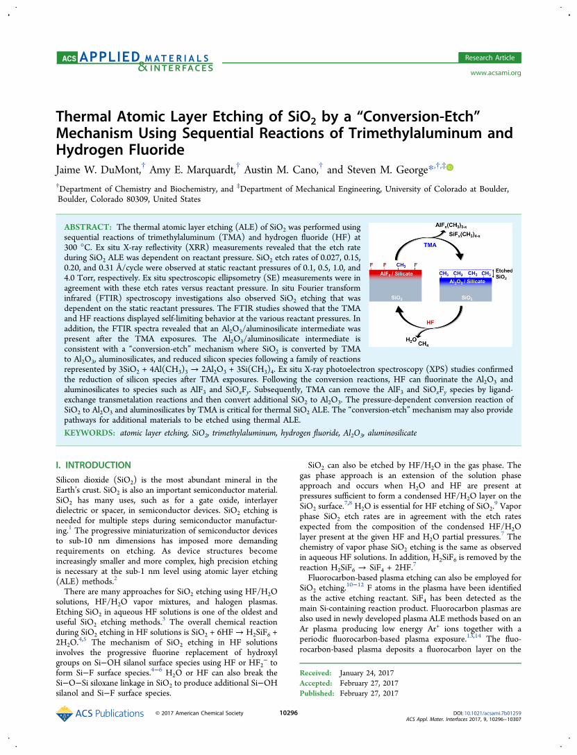
Thermal Atomic Layer Etching of SiO2 by a “Conversion-Etch”Mechanism Using Sequential Reactions of Trimethylaluminum andHydrogen FluorideJaime W. DuMont,† Amy E. Marquardt,† Austin M. Cano,† and Steven M. George*,†,‡
†Department of Chemistry and Biochemistry, and ‡Department of Mechanical Engineering, University of Colorado at Boulder,Boulder, Colorado 80309, United States
ABSTRACT: The thermal atomic layer etching (ALE) of SiO2 was performed usingsequential reactions of trimethylaluminum (TMA) and hydrogen fluoride (HF) at300 °C. Ex situ X-ray reflectivity (XRR) measurements revealed that the etch rateduring SiO2 ALE was dependent on reactant pressure. SiO2 etch rates of 0.027, 0.15,0.20, and 0.31 Å/cycle were observed at static reactant pressures of 0.1, 0.5, 1.0, and4.0 Torr, respectively. Ex situ spectroscopic ellipsometry (SE) measurements were inagreement with these etch rates versus reactant pressure. In situ Fourier transforminfrared (FTIR) spectroscopy investigations also observed SiO2 etching that wasdependent on the static reactant pressures. The FTIR studies showed that the TMAand HF reactions displayed self-limiting behavior at the various reactant pressures. Inaddition, the FTIR spectra revealed that an Al2O3/aluminosilicate intermediate waspresent after the TMA exposures. The Al2O3/aluminosilicate intermediate isconsistent with a “conversion-etch” mechanism where SiO2 is converted by TMAto Al2O3, aluminosilicates, and reduced silicon species following a family of reactionsrepresented by 3SiO2 + 4Al(CH3)3 → 2Al2O3 + 3Si(CH3)4. Ex situ X-ray photoelectron spectroscopy (XPS) studies confirmedthe reduction of silicon species after TMA exposures. Following the conversion reactions, HF can fluorinate the Al2O3 andaluminosilicates to species such as AlF3 and SiOxFy. Subsequently, TMA can remove the AlF3 and SiOxFy species by ligand-exchange transmetalation reactions and then convert additional SiO2 to Al2O3. The pressure-dependent conversion reaction ofSiO2 to Al2O3 and aluminosilicates by TMA is critical for thermal SiO2 ALE. The “conversion-etch” mechanism may also providepathways for additional materials to be etched using thermal ALE.
KEYWORDS: atomic layer etching, SiO2, trimethylaluminum, hydrogen fluoride, Al2O3, aluminosilicate
I. INTRODUCTION
Silicon dioxide (SiO2) is the most abundant mineral in theEarth’s crust. SiO2 is also an important semiconductor material.SiO2 has many uses, such as for a gate oxide, interlayerdielectric or spacer, in semiconductor devices. SiO2 etching isneeded for multiple steps during semiconductor manufactur-ing.1 The progressive miniaturization of semiconductor devicesto sub-10 nm dimensions has imposed more demandingrequirements on etching. As device structures becomeincreasingly smaller and more complex, high precision etchingis necessary at the sub-1 nm level using atomic layer etching(ALE) methods.2
There are many approaches for SiO2 etching using HF/H2Osolutions, HF/H2O vapor mixtures, and halogen plasmas.Etching SiO2 in aqueous HF solutions is one of the oldest anduseful SiO2 etching methods.3 The overall chemical reactionduring SiO2 etching in HF solutions is SiO2 + 6HF→ H2SiF6 +2H2O.
4,5 The mechanism of SiO2 etching in HF solutionsinvolves the progressive fluorine replacement of hydroxylgroups on Si−OH silanol surface species using HF or HF2
− toform Si−F surface species.4−6 H2O or HF can also break theSi−O−Si siloxane linkage in SiO2 to produce additional Si−OHsilanol and Si−F surface species.
SiO2 can also be etched by HF/H2O in the gas phase. Thegas phase approach is an extension of the solution phaseapproach and occurs when H2O and HF are present atpressures sufficient to form a condensed HF/H2O layer on theSiO2 surface.
7,8 H2O is essential for HF etching of SiO2.9 Vapor
phase SiO2 etch rates are in agreement with the etch ratesexpected from the composition of the condensed HF/H2Olayer present at the given HF and H2O partial pressures.7 Thechemistry of vapor phase SiO2 etching is the same as observedin aqueous HF solutions. In addition, H2SiF6 is removed by thereaction H2SiF6 → SiF4 + 2HF.7
Fluorocarbon-based plasma etching can also be employed forSiO2 etching.
10−12 F atoms in the plasma have been identifiedas the active etching reactant. SiF4 has been detected as themain Si-containing reaction product. Fluorocarbon plasmas arealso used in newly developed plasma ALE methods based on anAr plasma producing low energy Ar+ ions together with aperiodic fluorocarbon-based plasma exposure.13,14 The fluo-rocarbon-based plasma deposits a fluorocarbon layer on the
Received: January 24, 2017Accepted: February 27, 2017Published: February 27, 2017
Research Article
www.acsami.org
© 2017 American Chemical Society 10296 DOI: 10.1021/acsami.7b01259ACS Appl. Mater. Interfaces 2017, 9, 10296−10307
SiO2 surface. The Ar+ ion bombardment then desorbs thefluorocarbon layer and also removes a controlled amount of theSiO2 layer.Thermal ALE processes have been introduced recently for
Al2O3, HfO2, ZrO2, AlF3, and AlN ALE based on sequentialfluorination and ligand-exchange reactions.15−22 In thesethermal reactions, the metal oxide is first fluorinated toproduce the metal fluoride.17,19,22 The metal fluoride is thenremoved by a metal precursor in a ligand-exchange trans-metalation reaction.17,19,22 In this ligand-exchange reaction, themetal precursor accepts fluorine from the metal fluoride anddonates one of its ligands to the metal fluoride. The resultingreaction product formed from the metal fluoride can thendesorb from the surface if this metal species is stable andvolatile.20,22
In this paper, a new gas-phase thermal SiO2 ALE process isreported based on sequential exposures of Al(CH3)3(trimethylaluminum (TMA)) and HF. SiO2 film thicknesseswere measured versus number of ALE cycles using ex situspectroscopic ellipsometry to obtain the SiO2 etching rates.These studies determined the linearity of the SiO2 etching andthe dependence of the SiO2 etching on the TMA and HFreactant pressures. Ex situ X-ray photoelectron spectroscopy(XPS) measurements were also employed to determine thesilicon oxidation state after the TMA and HF reactions. Inaddition, in situ Fourier transform infrared (FTIR) spectros-copy measurements were used to measure the loss ofabsorbance from Si−O stretching vibrations and to monitorthe surfaces species present after each TMA and HF exposureat various pressures.Recent studies of ZnO ALE using TMA and HF as the
reactants have revealed a new “conversion-etch” reactionmechanism where a ZnO surface layer is converted to anAl2O3 surface layer and volatile Zn(CH3)2 reaction productsduring the TMA exposure.23 In this investigation, the FTIR andXPS studies determined that there was a similar conversion ofSiO2 to Al2O3 by TMA. The observation of Al2O3,aluminosilicate species, and silicon in reduced oxidation statesestablished that the “conversion-etch” mechanism also occursfor SiO2 ALE. In addition, the reactant pressures were criticalfor SiO2 ALE and larger etch rates occurred at higher reactantpressures. The generality of the “conversion-etch” mechanismcould expand the number of materials that can be etched usingthermal ALE methods.
II. EXPERIMENTAL SECTION1. Static Reactor, Silicon Wafers, and Ex Situ Film Analysis.
ALE reactions were performed in a hot wall ALD reactor.24 Aproportional-integral-derivative (PID) temperature controller (2604,Eurotherm) maintained the reaction temperature at 300 °C. Acapacitance manometer (Baratron 121A, MKS) monitored thepressure in the reactor. The starting SiO2 substrate was a thermalSiO2 layer with a thickness of 40 nm on Si(100) wafers with a diameterof 100 mm (University Wafer). The silicon wafers were cut intosamples with dimensions of 2.5 cm × 2.5 cm before the SiO2 ALE.The SiO2 ALE reactions were accomplished using sequential static
exposures of TMA (97%, Sigma-Aldrich) and HF derived from HF−pyridine (70 wt % HF, Sigma-Aldrich). HF−pyridine was transferredto a gold-plated stainless steel bubbler using a dry N2-filled glovebag.The TMA and HF−pyridine precursors were held at roomtemperature. Each reactant exposure consisted of a static dose of 20s followed by a purge of 120 s with 550 sccm of ultrahigh purity(UHP) N2. The total N2 gas flow of 550 sccm produced a basepressure of ∼2 Torr in the reactor during the purge steps. The N2,
precursor, and reaction byproducts were pumped by a mechanicalpump (Pascal 2010SD, Alcatel Adixen).
The ex situ X-ray reflectivity (XRR) scans were measured by a highresolution X-ray diffractometer (Bede D1, Jordan Valley Semi-conductors) using Cu Kα (λ = 1.540 Å) radiation. The filamentvoltage and current in the X-ray tube were 40 kV and 35 mA,respectively. A 5 arcsec step size and a 10 s acquisition time were usedfor recording all XRR scans with a range of 300−4500 arcsec. Theanalysis software (Bede REFS, Jordan Valley Semiconductors)determined film thickness, film density, and surface roughness byfitting the XRR scans.
Ellipsometry was performed using a spectroscopic ellipsometer (J.A. Woollam M-2000D). This ellipsometer has a spectral range of 240−1700 nm and utilizes an incidence angle of 75°. A Cauchy model wasused to determine the film thickness. This modeling was performedusing analysis software (CompleteEASE, J. A. Woollam). SiO2 filmthicknesses were measured at the same position on each silicon samplebefore and after etching.
Thermal SiO2 layers with a thickness of 40 nm on Si(100) wafers(University Wafer) were used for XPS analysis to determine thesurface species after TMA-only and TMA/HF exposures. These SiO2samples were exposed to 8 Torr of TMA for 5 min or 8 Torr of TMAfor 5 min followed by 4 Torr of HF for 10 min. After the static reactantexposures, the samples were immediately transferred to a PHI 5600 X-ray photoelectron spectroscopy (XPS) spectrometer to analyze thefilms. A SiO2 sample without TMA or HF exposures was also analyzedwith XPS.
A monochromatic Al Kα X-ray source (1486.6 eV) was used tocollect survey scans with a pass energy of 93.9 eV and step size of0.400 eV. An XPS software package (Auger Scan, RBD Instruments)was used to collect the XPS spectra. Casa XPS software (Casa XPS,Casa Software) was used for peak analysis of the C 1s, O 1s, Si 2p, Al2p, and F 1s XPS signals. All peaks were calibrated to the C 1s peakcentered at 284.8 eV.
The oxidation state of Si was determined through fitting the Si 2ppeak profile using Gaussian−Lorentzian line shapes after a Shirleybackground subtraction. XPS analysis of the SiO2 control sample wasused to determine the Si 2p binding energy position and full width athalf-maximum (fwhm) of the 4+ oxidation state peak. The bindingenergy (104.3 eV) and fwhm (2.1 eV) of the 4+ oxidation state wereimposed in the fittings of the TMA-only and TMA/HF exposedsamples. The binding energy positions for the 3+, 2+, 1+, and 0oxidation states were defined as −1, −2, −3, and −4 eV with respect tothe 4+ peak.25,26 The fwhm values of the 3+, 2+, 1+, and 0 oxidationstates were set to 1.2 ± 0.1, 1.1 ± 0.1, 1.0 ± 0.1, and 1.0 ± 0.1 eV,respectively.25−27
2. In Situ Fourier Transform Infrared (FTIR) SpectroscopyStudies. The surface chemistry during sequential exposures of TMA(97%, Sigma-Aldrich) and HF derived from HF−pyridine (70 wt %HF, Sigma-Aldrich) on SiO2 at 300 °C was studied using in situ FTIRspectroscopy. The in situ FTIR studies were performed in a reactorequipped with an FTIR spectrometer that has been describedpreviously.28 The FTIR experiments utilized high surface area Sinanoparticles (>98%, US Research Nanomaterials) with an averagediameter of 20−30 nm. The large surface area provided by thenanopowder sample improved the signal-to-noise ratio for infraredabsorption. The Si nanoparticles were mechanically pressed into atungsten grid support to facilitate the transmission FTIR measure-ments.29 The tungsten grid was 2 × 3 cm2, 50 μm thick, with 100 gridlines per inch.
The tungsten grid could be resistively heated using a dc powersupply (6268B, 20 V/20 A, Hewlett-Packard). The voltage output ofthe power supply was controlled by a PID temperature controller(Love Controls 16B, Dwyer Instruments). A type K thermocouple wasattached to the bottom of the tungsten grid with epoxy (Ceramabond571, Aremco) that attached and electrically isolated the thermocouple.To create a uniform SiO2 surface, the Si nanoparticles were annealed at650 °C for 1 h under ∼25 Torr of H2O vapor.
Figure 1a shows the absolute FTIR spectra of the SiO2 coating onthe Si nanoparticles before and after the H2O oxidation process.
ACS Applied Materials & Interfaces Research Article
DOI: 10.1021/acsami.7b01259ACS Appl. Mater. Interfaces 2017, 9, 10296−10307
10297
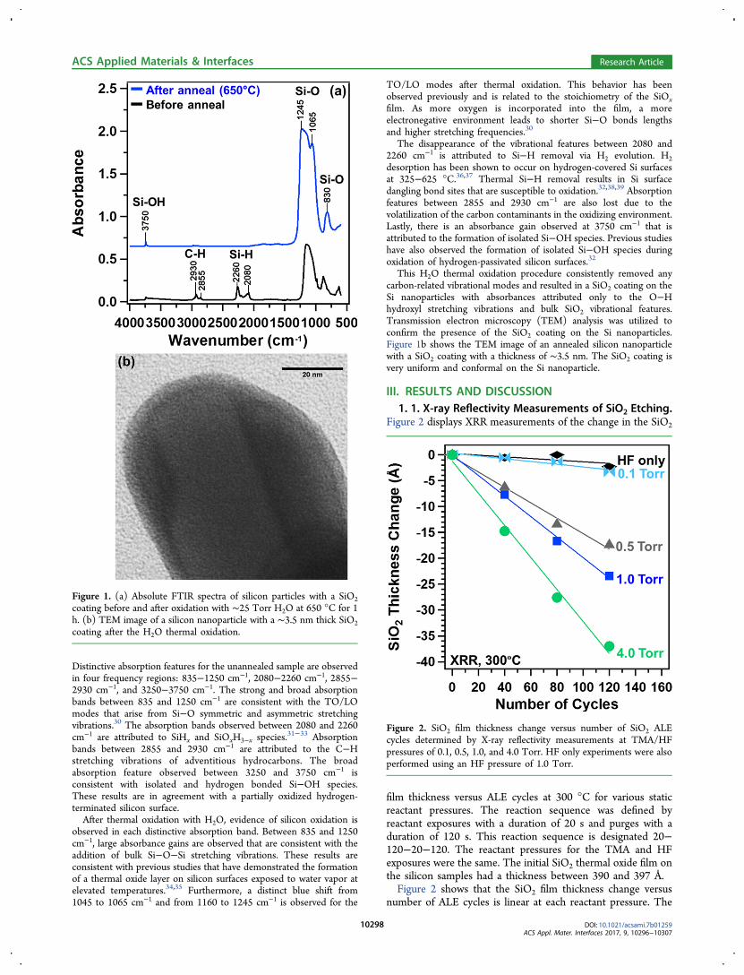
Distinctive absorption features for the unannealed sample are observedin four frequency regions: 835−1250 cm−1, 2080−2260 cm−1, 2855−2930 cm−1, and 3250−3750 cm−1. The strong and broad absorptionbands between 835 and 1250 cm−1 are consistent with the TO/LOmodes that arise from Si−O symmetric and asymmetric stretchingvibrations.30 The absorption bands observed between 2080 and 2260cm−1 are attributed to SiHx and SiOxH3−x species.31−33 Absorptionbands between 2855 and 2930 cm−1 are attributed to the C−Hstretching vibrations of adventitious hydrocarbons. The broadabsorption feature observed between 3250 and 3750 cm−1 isconsistent with isolated and hydrogen bonded Si−OH species.These results are in agreement with a partially oxidized hydrogen-terminated silicon surface.After thermal oxidation with H2O, evidence of silicon oxidation is
observed in each distinctive absorption band. Between 835 and 1250cm−1, large absorbance gains are observed that are consistent with theaddition of bulk Si−O−Si stretching vibrations. These results areconsistent with previous studies that have demonstrated the formationof a thermal oxide layer on silicon surfaces exposed to water vapor atelevated temperatures.34,35 Furthermore, a distinct blue shift from1045 to 1065 cm−1 and from 1160 to 1245 cm−1 is observed for the
TO/LO modes after thermal oxidation. This behavior has beenobserved previously and is related to the stoichiometry of the SiOxfilm. As more oxygen is incorporated into the film, a moreelectronegative environment leads to shorter Si−O bonds lengthsand higher stretching frequencies.30
The disappearance of the vibrational features between 2080 and2260 cm−1 is attributed to Si−H removal via H2 evolution. H2desorption has been shown to occur on hydrogen-covered Si surfacesat 325−625 °C.36,37 Thermal Si−H removal results in Si surfacedangling bond sites that are susceptible to oxidation.32,38,39 Absorptionfeatures between 2855 and 2930 cm−1 are also lost due to thevolatilization of the carbon contaminants in the oxidizing environment.Lastly, there is an absorbance gain observed at 3750 cm−1 that isattributed to the formation of isolated Si−OH species. Previous studieshave also observed the formation of isolated Si−OH species duringoxidation of hydrogen-passivated silicon surfaces.32
This H2O thermal oxidation procedure consistently removed anycarbon-related vibrational modes and resulted in a SiO2 coating on theSi nanoparticles with absorbances attributed only to the O−Hhydroxyl stretching vibrations and bulk SiO2 vibrational features.Transmission electron microscopy (TEM) analysis was utilized toconfirm the presence of the SiO2 coating on the Si nanoparticles.Figure 1b shows the TEM image of an annealed silicon nanoparticlewith a SiO2 coating with a thickness of ∼3.5 nm. The SiO2 coating isvery uniform and conformal on the Si nanoparticle.
III. RESULTS AND DISCUSSION1. 1. X-ray Reflectivity Measurements of SiO2 Etching.
Figure 2 displays XRR measurements of the change in the SiO2
film thickness versus ALE cycles at 300 °C for various staticreactant pressures. The reaction sequence was defined byreactant exposures with a duration of 20 s and purges with aduration of 120 s. This reaction sequence is designated 20−120−20−120. The reactant pressures for the TMA and HFexposures were the same. The initial SiO2 thermal oxide film onthe silicon samples had a thickness between 390 and 397 Å.Figure 2 shows that the SiO2 film thickness change versus
number of ALE cycles is linear at each reactant pressure. The
Figure 1. (a) Absolute FTIR spectra of silicon particles with a SiO2coating before and after oxidation with ∼25 Torr H2O at 650 °C for 1h. (b) TEM image of a silicon nanoparticle with a ∼3.5 nm thick SiO2coating after the H2O thermal oxidation.
Figure 2. SiO2 film thickness change versus number of SiO2 ALEcycles determined by X-ray reflectivity measurements at TMA/HFpressures of 0.1, 0.5, 1.0, and 4.0 Torr. HF only experiments were alsoperformed using an HF pressure of 1.0 Torr.
ACS Applied Materials & Interfaces Research Article
DOI: 10.1021/acsami.7b01259ACS Appl. Mater. Interfaces 2017, 9, 10296−10307
10298
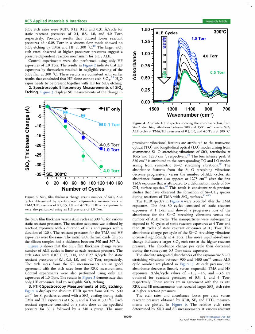
SiO2 etch rates were 0.027, 0.15, 0.20, and 0.31 Å/cycle forstatic reactant pressures of 0.1, 0.5, 1.0, and 4.0 Torr,respectively. Previous results that utilized lower reactantpressures of ∼0.08 Torr in a viscous flow mode showed noSiO2 etching by TMA and HF at 300 °C.18 The larger SiO2etch rates observed at higher precursor pressures suggest apressure-dependent reaction mechanism for SiO2 ALE.Control experiments were also performed using only HF
exposures of 1.0 Torr. The results in Figure 2 indicate that HFexposures by themselves resulted in negligible etching of theSiO2 film at 300 °C. These results are consistent with earlierresults that concluded that HF alone cannot etch SiO2.
7,9 H2Ovapor needs to be present together with HF for SiO2 etching.2. Spectroscopic Ellipsometry Measurements of SiO2
Etching. Figure 3 displays SE measurements of the change in
the SiO2 film thickness versus ALE cycles at 300 °C for variousstatic reactant pressures. The reaction sequence was defined byreactant exposures with a duration of 20 s and purges with aduration of 120 s. The reactant pressures for the TMA and HFexposures were the same. The initial SiO2 thermal oxide film onthe silicon samples had a thickness between 390 and 397 Å.Figure 3 shows that the SiO2 film thickness change versus
number of ALE cycles is linear at each reactant pressure. Theetch rates were 0.07, 0.17, 0.18, and 0.27 Å/cycle for staticreactant pressures of 0.1, 0.5, 1.0, and 4.0 Torr, respectively.The etch rates from the SE measurements are in goodagreement with the etch rates from the XRR measurements.Control experiments were also performed using only HFexposures of 1.0 Torr. The results in Figure 3 demonstrate thatonly HF exposures lead to negligible SiO2 etching.3. FTIR Spectroscopy Measurements of SiO2 Etching.
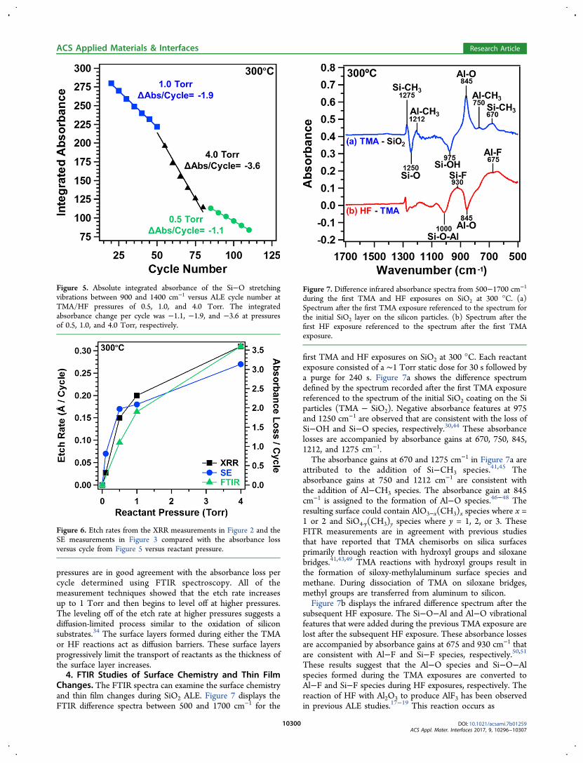
Figure 4 displays the absolute FTIR spectra from 700 to 1500cm−1 for Si particles covered with a SiO2 coating during staticTMA and HF exposures at 0.5, 1, and 4 Torr at 300 °C. Eachreactant exposure consisted of a static dose at the specifiedpressure for 30 s followed by a 240 s purge. The most
prominent vibrational features are attributed to the transverseoptical (TO) and longitudinal optical (LO) modes arising fromasymmetric Si−O stretching vibrations of SiO4 tetrahedra at1065 and 1230 cm−1, respectively.30 The less intense peak at820 cm−1 is attributed to the corresponding TO and LO modesarising from symmetric Si−O stretching vibrations.30 Theabsorbance features from the Si−O stretching vibrationsdecrease progressively versus the number of ALE cycles. Anabsorbance feature also appears at 1275 cm−1 after the firstTMA exposure that is attributed to a deformation mode of Si−CH3 surface species.40 This result is consistent with previousstudies that have observed the formation of Si−CH3 speciesduring reactions of TMA with SiO2 surfaces.
41−43
The FTIR spectra in Figure 4 were recorded after the TMAexposures. The first 50 cycles consisted of static reactantexposures at 1 Torr and showed a progressive loss of theabsorbance for the Si−O stretching vibrations versus thenumber of ALE cycles. The nanoparticles were subsequentlyexposed to 30 cycles of static reactant exposures at 4 Torr andthen 30 cycles of static reactant exposures at 0.5 Torr. Theabsorbance change per cycle of the Si−O stretching vibrationsincreased significantly at 4 Torr. This more rapid absorbancechange indicates a larger SiO2 etch rate at the higher reactantpressure. The absorbance change per cycle then decreasedduring the subsequent 0.5 Torr static exposures.The absolute integrated absorbances of the asymmetric Si−O
stretching vibrations between 900 and 1400 cm−1 versus ALEcycle number are plotted in Figure 5. At each pressure, theabsorbance decreases linearly versus sequential TMA and HFexposures. ΔAbs/cycle values of −1.1, −1.9, and −3.6 areobtained for reactant pressures of 0.5, 1, and 4 Torr,respectively. These results are in agreement with the ex situXRR and SE measurements that revealed larger SiO2 etch ratesat higher reactant pressures.The etch rates and absorbance losses per cycle versus
reactant pressure obtained by XRR, SE, and FTIR measure-ments are plotted in Figure 6. The relative etch ratesdetermined by XRR and SE measurements at various reactant
Figure 3. SiO2 film thickness change versus number of SiO2 ALEcycles determined by spectroscopic ellipsometry measurements atTMA/HF pressures of 0.1, 0.5, 1.0, and 4.0 Torr. HF only experimentswere also performed using an HF pressure of 1.0 Torr.
Figure 4. Absolute FTIR spectra showing the absorbance loss fromSi−O stretching vibrations between 700 and 1500 cm−1 versus SiO2ALE cycles at TMA/HF pressures of 0.5, 1.0, and 4.0 Torr at 300 °C.
ACS Applied Materials & Interfaces Research Article
DOI: 10.1021/acsami.7b01259ACS Appl. Mater. Interfaces 2017, 9, 10296−10307
10299
pressures are in good agreement with the absorbance loss percycle determined using FTIR spectroscopy. All of themeasurement techniques showed that the etch rate increasesup to 1 Torr and then begins to level off at higher pressures.The leveling off of the etch rate at higher pressures suggests adiffusion-limited process similar to the oxidation of siliconsubstrates.34 The surface layers formed during either the TMAor HF reactions act as diffusion barriers. These surface layersprogressively limit the transport of reactants as the thickness ofthe surface layer increases.4. FTIR Studies of Surface Chemistry and Thin Film
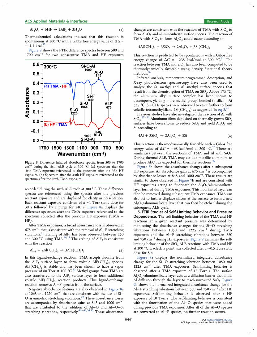
Changes. The FTIR spectra can examine the surface chemistryand thin film changes during SiO2 ALE. Figure 7 displays theFTIR difference spectra between 500 and 1700 cm−1 for the
first TMA and HF exposures on SiO2 at 300 °C. Each reactantexposure consisted of a ∼1 Torr static dose for 30 s followed bya purge for 240 s. Figure 7a shows the difference spectrumdefined by the spectrum recorded after the first TMA exposurereferenced to the spectrum of the initial SiO2 coating on the Siparticles (TMA − SiO2). Negative absorbance features at 975and 1250 cm−1 are observed that are consistent with the loss ofSi−OH and Si−O species, respectively.30,44 These absorbancelosses are accompanied by absorbance gains at 670, 750, 845,1212, and 1275 cm−1.The absorbance gains at 670 and 1275 cm−1 in Figure 7a are
attributed to the addition of Si−CH3 species.41,45 Theabsorbance gains at 750 and 1212 cm−1 are consistent withthe addition of Al−CH3 species. The absorbance gain at 845cm−1 is assigned to the formation of Al−O species.46−48 Theresulting surface could contain AlO3−x(CH3)x species where x =1 or 2 and SiO4‑y(CH3)y species where y = 1, 2, or 3. TheseFITR measurements are in agreement with previous studiesthat have reported that TMA chemisorbs on silica surfacesprimarily through reaction with hydroxyl groups and siloxanebridges.41,43,49 TMA reactions with hydroxyl groups result inthe formation of siloxy-methylaluminum surface species andmethane. During dissociation of TMA on siloxane bridges,methyl groups are transferred from aluminum to silicon.Figure 7b displays the infrared difference spectrum after the
subsequent HF exposure. The Si−O−Al and Al−O vibrationalfeatures that were added during the previous TMA exposure arelost after the subsequent HF exposure. These absorbance lossesare accompanied by absorbance gains at 675 and 930 cm−1 thatare consistent with Al−F and Si−F species, respectively.50,51
These results suggest that the Al−O species and Si−O−Alspecies formed during the TMA exposures are converted toAl−F and Si−F species during HF exposures, respectively. Thereaction of HF with Al2O3 to produce AlF3 has been observedin previous ALE studies.17−19 This reaction occurs as
Figure 5. Absolute integrated absorbance of the Si−O stretchingvibrations between 900 and 1400 cm−1 versus ALE cycle number atTMA/HF pressures of 0.5, 1.0, and 4.0 Torr. The integratedabsorbance change per cycle was −1.1, −1.9, and −3.6 at pressuresof 0.5, 1.0, and 4.0 Torr, respectively.
Figure 6. Etch rates from the XRR measurements in Figure 2 and theSE measurements in Figure 3 compared with the absorbance lossversus cycle from Figure 5 versus reactant pressure.
Figure 7. Difference infrared absorbance spectra from 500−1700 cm−1
during the first TMA and HF exposures on SiO2 at 300 °C. (a)Spectrum after the first TMA exposure referenced to the spectrum forthe initial SiO2 layer on the silicon particles. (b) Spectrum after thefirst HF exposure referenced to the spectrum after the first TMAexposure.
ACS Applied Materials & Interfaces Research Article
DOI: 10.1021/acsami.7b01259ACS Appl. Mater. Interfaces 2017, 9, 10296−10307
10300
+ → +Al O 6HF 2AlF 3H O2 3 3 2 (1)
Thermochemical calculations indicate that this reaction isspontaneous at 300 °C with a Gibbs free energy value of ΔG =−41.1 kcal.52
Figure 8 shows the FTIR difference spectra between 500 and1700 cm−1 for two consecutive TMA and HF exposures
recorded during the sixth ALE cycle at 300 °C. These differencespectra are referenced using the spectra after the previousreactant exposure and are displaced for clarity in presentation.Each reactant exposure consisted of a ∼1 Torr static dose for30 s followed by a purge for 240 s. Figure 8a displays thedifference spectrum after the TMA exposure referenced to thespectrum collected after the previous HF exposure (TMA −HF).After TMA exposures, a broad absorbance loss is observed at
675 cm−1 that is consistent with the removal of Al−F stretchingvibrations.51 Etching of AlF3 has been observed between 250and 300 °C using TMA.16,18 The etching of AlF3 is consistentwith the reaction
+ →AlF 2Al(CH ) 3AlF(CH )3 3 3 3 2 (2)
In this ligand-exchange reaction, TMA accepts fluorine fromthe AlF3 surface layer to form volatile AlF(CH3)2 species.AlF(CH3)2 is stable and has been shown to have a vaporpressure of 80 Torr at 100 °C.53 Methyl groups from TMA arealso transferred to the AlF3 surface layer to form additionalvolatile AlF(CH3)2 reaction products. This ligand-exchangereaction removes Al−F species from the surface.Negative absorbance features are also observed in Figure 8a
at 1065 and 1220 cm−1 that are consistent with the loss of Si−O asymmetric stretching vibrations.30 These absorbance lossesare accompanied by absorbance gains at 845 and 1000 cm−1
that are attributed to the addition of Al−O and Al−O−Sistretching vibrations, respectively.46−48,54,55 These absorbance
changes are consistent with the reaction of TMA with SiO2 toform Al2O3 and aluminosilicate surface species. The reaction ofTMA with SiO2 to form Al2O3 could occur according to
+ → +4Al(CH ) 3SiO 2Al O 3Si(CH )3 3 2 2 3 3 4 (3)
This reaction is predicted to be spontaneous with a Gibbs freeenergy change of ΔG = −235 kcal/mol at 300 °C.52 Thereaction between TMA and SiO2 has also been computed to bethermodynamically favorable using density functional theorymethods.56
Infrared analysis, temperature-programmed desorption, andX-ray photoelectron spectroscopy have also been used toanalyze the Si−methyl and Al−methyl surface species thatresult from the chemisorption of TMA on SiO2. Above 175 °C,the aluminum alkyl surface complex has been shown todecompose, yielding more methyl groups bonded to silicon. At325 °C, Si−CH3 species were observed to react further to formvolatile tetramethylsilane (Si(CH3)4) as suggested in eq 3.41
Previous studies have also investigated the reaction of Al withSiO2.
57−59 Aluminum films deposited on thermally grown SiO2surfaces have been shown to reduce SiO2 and yield Al2O3 andSi according to
+ → +4Al 3SiO 2Al O 3Si2 2 3 (4)
This reaction is thermodynamically favorable with a Gibbs freeenergy value of ΔG = −68 kcal/mol at 300 °C.52 There aresimilarities between the reactions of TMA and Al with SiO2.During thermal ALE, TMA may act like metallic aluminum toproduce Al2O3 as expected for thermite reactions.60
Figure 8b shows the absorbance changes after a subsequentHF exposure. An absorbance gain at 675 cm−1 is accompaniedby absorbance losses at 845 and 1000 cm−1. These results aresimilar to those observed in Figure 7b and are consistent withHF exposures acting to fluorinate the Al2O3/aluminosilicatelayer formed during TMA exposures. This fluorinated layer canthen be removed during subsequent TMA exposures. TMA canalso act to further displace silicon at the surface to form a newAl2O3/aluminosilicate layer that can then be etched during thesubsequent ALE cycle.
5. FTIR Studies of Self-Limiting Behavior and PressureDependence. The self-limiting behavior of the TMA and HFreactions at a given reactant pressure was determined bymonitoring the absorbance changes for the Si−O stretchingvibrations between 1050 and 1225 cm−1 during TMAexposures and the Al−F stretching vibrations between 550and 750 cm−1 during HF exposures. Figure 9 examines the self-limiting behavior of the SiO2 ALE reactions with TMA and HFat 300 °C. Each data point was collected after a ∼0.5 Torr staticdose for 5 s.Figure 9a displays the normalized integrated absorbance
change for the Si−O stretching vibration between 1050 and1225 cm−1 after TMA exposures. Self-limiting behavior isobserved after a TMA exposure of 15 Torr s. The surfaceAl2O3/aluminosilicate layer acts as a diffusion barrier that limitsAl diffusion through the layer to reach unreacted SiO2. Figure9b shows the normalized integrated absorbance change for theAl−F stretching vibrations between 550 and 750 cm−1 after HFexposures. Self-limiting behavior is observed after a HFexposure of 10 Torr s. The self-limiting behavior is consistentwith the fluorination of the Al−O species that were addedduring previous TMA exposures. After all of the Al−O speciesare converted to Al−F species, no further reaction occurs.
Figure 8. Difference infrared absorbance spectra from 500 to 1700cm−1 during the sixth ALE cycle at 300 °C. (a) Spectrum after thesixth TMA exposure referenced to the spectrum after the fifth HFexposure. (b) Spectrum after the sixth HF exposure referenced to thespectrum after the sixth TMA exposure.
ACS Applied Materials & Interfaces Research Article
DOI: 10.1021/acsami.7b01259ACS Appl. Mater. Interfaces 2017, 9, 10296−10307
10301
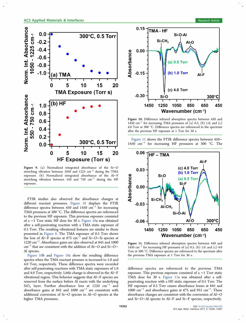
FTIR studies also observed the absorbance changes atdifferent reactant pressures. Figure 10 displays the FTIRdifference spectra between 450 and 1450 cm−1 for increasingTMA pressures at 300 °C. The difference spectra are referencedto the previous HF exposure. This previous exposure consistedof a ∼1 Torr static HF dose for 30 s. Figure 10a was obtainedafter a self-passivating reaction with a TMA static exposure of0.5 Torr. The resulting vibrational features are similar to thosepresented in Figure 8. The TMA exposure of 0.5 Torr showsthe loss of Al−F species at 675 cm−1 and Si−O−Si species at1220 cm−1. Absorbance gains are also observed at 845 and 1000cm−1 that are consistent with the addition of Al−O and Si−O−Al species.Figure 10b and Figure 10c show the resulting difference
spectra when the TMA reactant pressure is increased to 1.0 and4.0 Torr, respectively. These difference spectra were recordedafter self-passivating reactions with TMA static exposures of 1.0and 4.0 Torr, respectively. Little change is observed in the Al−Fvibrational region. This behavior suggests that Al−F species areremoved from the surface before Al reacts with the underlyingSiO2 layer. Further absorbance loss at 1220 cm−1 andabsorbance gains at 845 and 1000 cm−1 are consistent withadditional conversion of Si−O species to Al−O species at thehigher TMA pressures.
Figure 11 shows the FTIR difference spectra between 450−1450 cm−1 for increasing HF pressures at 300 °C. The
difference spectra are referenced to the previous TMAexposure. This previous exposure consisted of a ∼1 Torr staticTMA dose for 30 s. Figure 11a was obtained after a self-passivating reaction with a HF static exposure of 0.5 Torr. TheHF exposure of 0.5 Torr causes absorbance losses at 845 and1000 cm−1 and absorbance gains at 675 and 955 cm−1. Theseabsorbance changes are consistent with the conversion of Al−Oand Si−O−Al species to Al−F and Si−F species, respectively.
Figure 9. (a) Normalized integrated absorbance of the Si−Ostretching vibration between 1050 and 1225 cm−1 during the TMAexposure. (b) Normalized integrated absorbance of the Al−Fstretching vibration between 550 and 750 cm−1 during the HFexposure.
Figure 10. Difference infrared absorption spectra between 450 and1450 cm−1 for increasing TMA pressures of (a) 0.5, (b) 1.0, and (c)4.0 Torr at 300 °C. Difference spectra are referenced to the spectrumafter the previous HF exposure at 1 Torr for 30 s.
Figure 11. Difference infrared absorption spectra between 450 and1450 cm−1 for increasing HF pressures of (a) 0.5. (b) 1.0. and (c) 4.0Torr at 300 °C. Difference spectra are referenced to the spectrum afterthe previous TMA exposure at 1 Torr for 30 s.
ACS Applied Materials & Interfaces Research Article
DOI: 10.1021/acsami.7b01259ACS Appl. Mater. Interfaces 2017, 9, 10296−10307
10302
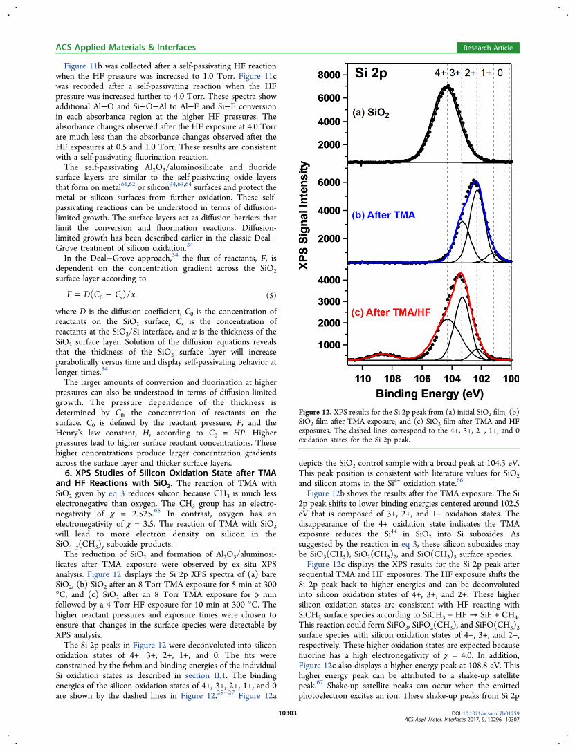
Figure 11b was collected after a self-passivating HF reactionwhen the HF pressure was increased to 1.0 Torr. Figure 11cwas recorded after a self-passivating reaction when the HFpressure was increased further to 4.0 Torr. These spectra showadditional Al−O and Si−O−Al to Al−F and Si−F conversionin each absorbance region at the higher HF pressures. Theabsorbance changes observed after the HF exposure at 4.0 Torrare much less than the absorbance changes observed after theHF exposures at 0.5 and 1.0 Torr. These results are consistentwith a self-passivating fluorination reaction.The self-passivating Al2O3/aluminosilicate and fluoride
surface layers are similar to the self-passivating oxide layersthat form on metal61,62 or silicon34,63,64 surfaces and protect themetal or silicon surfaces from further oxidation. These self-passivating reactions can be understood in terms of diffusion-limited growth. The surface layers act as diffusion barriers thatlimit the conversion and fluorination reactions. Diffusion-limited growth has been described earlier in the classic Deal−Grove treatment of silicon oxidation.34
In the Deal−Grove approach,34 the flux of reactants, F, isdependent on the concentration gradient across the SiO2surface layer according to
= −F D C C x( )/0 s (5)
where D is the diffusion coefficient, C0 is the concentration ofreactants on the SiO2 surface, Cs is the concentration ofreactants at the SiO2/Si interface, and x is the thickness of theSiO2 surface layer. Solution of the diffusion equations revealsthat the thickness of the SiO2 surface layer will increaseparabolically versus time and display self-passivating behavior atlonger times.34
The larger amounts of conversion and fluorination at higherpressures can also be understood in terms of diffusion-limitedgrowth. The pressure dependence of the thickness isdetermined by C0, the concentration of reactants on thesurface. C0 is defined by the reactant pressure, P, and theHenry’s law constant, H, according to C0 = HP. Higherpressures lead to higher surface reactant concentrations. Thesehigher concentrations produce larger concentration gradientsacross the surface layer and thicker surface layers.6. XPS Studies of Silicon Oxidation State after TMA
and HF Reactions with SiO2. The reaction of TMA withSiO2 given by eq 3 reduces silicon because CH3 is much lesselectronegative than oxygen. The CH3 group has an electro-negativity of χ = 2.525.65 In contrast, oxygen has anelectronegativity of χ = 3.5. The reaction of TMA with SiO2will lead to more electron density on silicon in theSiO4−y(CH3)y suboxide products.The reduction of SiO2 and formation of Al2O3/aluminosi-
licates after TMA exposure were observed by ex situ XPSanalysis. Figure 12 displays the Si 2p XPS spectra of (a) bareSiO2, (b) SiO2 after an 8 Torr TMA exposure for 5 min at 300°C, and (c) SiO2 after an 8 Torr TMA exposure for 5 minfollowed by a 4 Torr HF exposure for 10 min at 300 °C. Thehigher reactant pressures and exposure times were chosen toensure that changes in the surface species were detectable byXPS analysis.The Si 2p peaks in Figure 12 were deconvoluted into silicon
oxidation states of 4+, 3+, 2+, 1+, and 0. The fits wereconstrained by the fwhm and binding energies of the individualSi oxidation states as described in section II.1. The bindingenergies of the silicon oxidation states of 4+, 3+, 2+, 1+, and 0are shown by the dashed lines in Figure 12.25−27 Figure 12a
depicts the SiO2 control sample with a broad peak at 104.3 eV.This peak position is consistent with literature values for SiO2and silicon atoms in the Si4+ oxidation state.66
Figure 12b shows the results after the TMA exposure. The Si2p peak shifts to lower binding energies centered around 102.5eV that is composed of 3+, 2+, and 1+ oxidation states. Thedisappearance of the 4+ oxidation state indicates the TMAexposure reduces the Si4+ in SiO2 into Si suboxides. Assuggested by the reaction in eq 3, these silicon suboxides maybe SiO3(CH3), SiO2(CH3)2, and SiO(CH3)3 surface species.Figure 12c displays the XPS results for the Si 2p peak after
sequential TMA and HF exposures. The HF exposure shifts theSi 2p peak back to higher energies and can be deconvolutedinto silicon oxidation states of 4+, 3+, and 2+. These highersilicon oxidation states are consistent with HF reacting withSiCH3 surface species according to SiCH3 + HF → SiF + CH4.This reaction could form SiFO3, SiFO2(CH3), and SiFO(CH3)2surface species with silicon oxidation states of 4+, 3+, and 2+,respectively. These higher oxidation states are expected becausefluorine has a high electronegativity of χ = 4.0. In addition,Figure 12c also displays a higher energy peak at 108.8 eV. Thishigher energy peak can be attributed to a shake-up satellitepeak.67 Shake-up satellite peaks can occur when the emittedphotoelectron excites an ion. These shake-up peaks from Si 2p
Figure 12. XPS results for the Si 2p peak from (a) initial SiO2 film, (b)SiO2 film after TMA exposure, and (c) SiO2 film after TMA and HFexposures. The dashed lines correspond to the 4+, 3+, 2+, 1+, and 0oxidation states for the Si 2p peak.
ACS Applied Materials & Interfaces Research Article
DOI: 10.1021/acsami.7b01259ACS Appl. Mater. Interfaces 2017, 9, 10296−10307
10303
can be observed when Si is present in a siloxane polymerstructure.67
The reduction of SiO2 and formation of Al2O3/aluminosi-licates after TMA exposure were also monitored by XPSanalysis of the Si 2p XPS spectra after a 4 Torr TMA exposureon SiO2 for 20 s at 300 °C. The Si 2p XPS spectra displayed ashift from the 4+ oxidation state for SiO2 to a distribution of4+, 3+, 2+, and 1+ oxidation states after the TMA exposure.The peak of the spectrum occurred at the 3+ oxidation statecompared with a peak at the 2+ oxidation state for the TMAexposure at 8 Torr shown in Figure 12b. The Si 2p XPSspectrum after a 4 Torr TMA exposure on SiO2 for 20 sfollowed by a 4 Torr HF exposure for 20 s at 300 °C displayeda shift back to higher oxidation states similar to the resultsshown in Figure 12c.The Al 2p XPS peak was also consistent with the formation
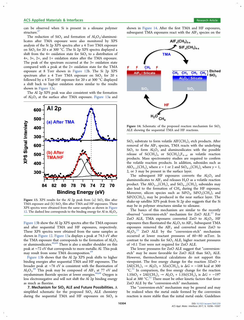
of Al2O3 at the surface after TMA exposure. Figure 13a and
Figure 13b show the Al 2p XPS spectra after the TMA exposureand after sequential TMA and HF exposures, respectively.These XPS spectra were obtained from the same samples asshown in Figure 12. Figure 13a displays a peak at 74.3 eV afterthe TMA exposure that corresponds to the formation of Al2O3or aluminosilicates.66,68 There is also a smaller shoulder on thispeak at ∼72 eV that corresponds to more metallic Al. This peakmay result from some TMA decomposition.69
Figure 13b shows that the Al 2p XPS peak shifts to higherbinding energies after sequential TMA and HF exposures. Thebroader peak at ∼76 eV is consistent with the fluorination ofAl2O3.
68 This peak may be composed of AlF3 at 77 eV andoxyaluminum fluoride species at lower energies.66,68 Oxygen isless electronegative and will not shift the Al 2p binding energyas much as fluorine.7. Mechanism for SiO2 ALE and Future Possibilities. A
simplified schematic for the proposed SiO2 ALE chemistryduring the sequential TMA and HF exposures on SiO2 is
shown in Figure 14. After the first TMA and HF exposures,subsequent TMA exposures react with the AlF3 species on the
SiO2 substrate to form volatile AlF(CH3)2 etch products. Afterremoval of the AlF3 species, TMA reacts with the underlyingSiO2 to form Al2O3 and aluminosilicates with the possiblerelease of Si(CH3)4 or Si(CH3)xF4−x, as volatile reactionproducts. Mass spectrometry studies are required to confirmthe volatile reaction products. In addition, suboxides such asAlO3−x(CH3)x where x = 1 or 2 and SiO4−y(CH3)y where y = 1,2, or 3 may be present in the surface layer.The subsequent HF exposures converts the Al2O3 and
aluminosilicates to AlF3 and releases H2O as a volatile reactionproduct. The AlO3−x(CH3)x and SiO4−y(CH3)y suboxides mayalso lead to the formation of CH4 during the HF exposure.Moreover, silicon species such as SiFO3, SiFO2(CH3), andSiFO(CH3)2 may be produced in the near surface layer. Theshake-up satellite XPS peak from Si 2p also suggests that the Simay be in polymer structures similar to siloxane.The basics of this mechanism are similar to the recently
observed “conversion-etch” mechanism for ZnO ALE.23 ForZnO ALE, TMA exposures converted ZnO to Al2O3. HFexposures then fluorinated the Al2O3 to AlF3. Subsequent TMAexposures removed the AlF3 and converted more ZnO toAl2O3.
23 ZnO ALE by the “conversion-etch” mechanismoccurred at lower reactant pressures of 60−80 mTorr. Incontrast to the results for SiO2 ALE, higher reactant pressuresof >0.1 Torr were not required for ZnO ALE.The lower pressures for ZnO ALE suggest that “conversion-
etch” may be more favorable for ZnO ALE than SiO2 ALE.However, thermochemical calculations do not support thisviewpoint. The free energy change for the reaction 3ZnO +2Al(CH3)3 → Al2O3 + 3Zn(CH3)2 is ΔG = −168 kcal at 300°C.52 In comparison, the free energy change for the reaction1.5SiO2 + 2Al(CH3)3 → Al2O3 + 1.5Si(CH3)4 is ΔG = −197kcal at 300 °C.52 There must be other kinetic factors that favorZnO ALE by the “conversion-etch” mechanism.The “conversion-etch” mechanism may be general and may
be realized when the metal oxide formed by the conversionreaction is more stable than the initial metal oxide. Guidelines
Figure 13. XPS results for the Al 2p peak from (a) SiO2 film afterTMA exposure and (b) SiO2 film after TMA and HF exposures. TheseXPS spectra were obtained from the same samples as shown in Figure12. The dashed line corresponds to the binding energy for Al in Al2O3.
Figure 14. Schematic of the proposed reaction mechanism for SiO2ALE showing the sequential TMA and HF reactions.
ACS Applied Materials & Interfaces Research Article
DOI: 10.1021/acsami.7b01259ACS Appl. Mater. Interfaces 2017, 9, 10296−10307
10304
for determining the relative stability of metal oxides can beobtained from thermochemical calculations or Ellinghamdiagrams.70 Some materials may not have viable pathways forthermal ALE because the ligand-exchange reactions may notproduce stable and volatile reaction products.20 By convertingthe initial material to a different material, the “conversion-etch”mechanism may enlarge the number of materials that can beetched using thermal ALE. For example, TMA is anticipated toconvert other metal oxides, such as SnO2 and In2O3, to Al2O3.
23
Thermal Al2O3 ALE has been demonstrated using HF andeither Sn(acac)2 or TMA as the reactants.17−19 Likewise, TMAis expected to convert various nitrides, such as Si3N4, to AlN.23
Thermal AlN ALE has been demonstrated using HF andSn(acac)2 as the reactants.21
Thermal SiO2 ALE also suggests a possible procedure forthermal Si ALE. The silicon surface can first be oxidized to forma self-passivating oxide layer on the silicon surface.63,64 Theresulting SiO2 layer can then be etched by the “conversion-etch” mechanism using sequential TMA and HF exposures. Byrepetition of the silicon oxidation and sequential TMA and HFexposures, silicon should be etched with atomic layer precision.Similar procedures may also be defined for the thermal ALE ofmetals using sequential oxidation, fluorination, and ligand-exchange reactions.
IV. CONCLUSIONS
Sequential reactions of trimethylaluminum (TMA) and hydro-gen fluoride (HF) were employed for the thermal atomic layeretching (ALE) of SiO2 at 300 °C. The etch rates during SiO2ALE were dependent on reactant pressures. SiO2 etch rates of0.027, 0.15, 0.20, and 0.31 Å/cycle were observed at staticreactant pressures of 0.1, 0.5, 1.0, and 4.0 Torr, respectively, byex situ X-ray reflectivity measurements. A similar increase inSiO2 etch rate with reactant pressure was confirmed by ex situspectroscopic ellipsometry measurements. The pressuredependence of the etch rate for SiO2 ALE was also observedby in situ FTIR studies. In addition, the FTIR measurementsmonitored the pressure-dependent conversion of the SiO2surface to an Al2O3/aluminosilicate layer. Ex situ XPSmeasurements also monitored the reduction of the siliconoxidation state after the TMA reaction.The Al2O3/aluminosilicate intermediate is attributed to the
conversion of SiO2 to Al2O3 and reduced silicon species by theTMA exposure according to reactions like 3SiO2 + 4Al(CH3)3→ 2Al2O3 + 3Si(CH3)4. The HF exposure can then fluorinateAl2O3 to AlF3 and form silicon fluoride species after thisconversion reaction. Subsequently, the next TMA exposure canremove AlF3 by a ligand-exchange transmetalation reaction andthen convert additional SiO2 to Al2O3 and reduced siliconspecies. The sequential TMA and HF reactions lead to SiO2ALE because the individual TMA and HF reactions display self-limiting behavior at the various reactant pressures.The pressure-dependent conversion reaction of the SiO2
surface to an Al2O3/aluminosilicate layer by TMA is critical forthermal SiO2 ALE. The “conversion-etch” mechanism for SiO2ALE is observed at reactant pressures of >0.1 Torr. Otherconversion reactions will be able to transform initial materialsthat cannot be etched to different materials that may havepossible etching pathways. The “conversion-etch” mechanismwill increase the number of materials that can be etched bythermal ALE methods. Oxidation and conversion reactions mayalso lead to procedures for thermal Si ALE.
■ AUTHOR INFORMATION
Corresponding Author*E-mail: [email protected]. Phone: 303-492-3398.Fax: 303-492-5894.
ORCIDSteven M. George: 0000-0003-0253-9184NotesThe authors declare no competing financial interest.
■ ACKNOWLEDGMENTS
This research was funded by the National Science Foundationby Grants CHE-1306131 and CHE-1609554 and the DefenseAdvanced Projects Agency (DARPA) by Grant W911NF-13-1-0041. The authors thank Huaxing Sun for the XPS measure-ments. The authors also thank Joel Clancey for assistance withthe TEM analysis of the silicon nanoparticles.
■ REFERENCES(1) Nojiri, K. Dry Etching Technology for Semiconductors; Springer:Heidelberg, Germany, 2012.(2) Carver, C. T.; Plombon, J. J.; Romero, P. E.; Suri, S.; Tronic, T.A.; Turkot, R. B. Atomic Layer Etching: An Industry Perspective. ECSJ. Solid State Sci. Technol. 2015, 4, N5005−N5009.(3) Blumberg, A. A.; Stavrinou, S. C. Tabulated Functions forHeterogeneous Reaction Rates - The Attack of Vitreous Silica byHydrofluoric Acid. J. Phys. Chem. 1960, 64, 1438−1442.(4) Monk, D. J.; Soane, D. S.; Howe, R. T. A Review of the ChemicalReaction Mechanisma and Kinetics for Hydrofluoric Acid Etching ofSilicon Dioxide for Surface Micromachining Applications. Thin SolidFilms 1993, 232, 1−12.(5) Spierings, G. A. C. M. Wet Chemical Etching of SIlicate-Glassesin Hydrofluoric Acid Based Solutions. J. Mater. Sci. 1993, 28, 6261−6273.(6) Knotter, D. M. Etching Mechanism of Vitreous Silicon Dioxide inHF-Based Solutions. J. Am. Chem. Soc. 2000, 122, 4345−4351.(7) Helms, C. R.; Deal, B. E. Mechanisms of the HF/H2O VaporPhase Etching of SiO2. J. Vac. Sci. Technol., A 1992, 10, 806−811.(8) Vanderheide, P. A. M.; Baan Hofman, M. J.; Ronde, H. J. Etchingof Thin SiO2 Layers Using Wet HF Gas. J. Vac. Sci. Technol., A 1989, 7,1719−1723.(9) Kang, J. K.; Musgrave, C. B. The Mechanism of HF/H2OChemical Etching of SiO2. J. Chem. Phys. 2002, 116, 275−280.(10) Mogab, C. J.; Adams, A. C.; Flamm, D. L. Plasma Etching of Siand SiO2 - Effect of Oxygen Additions to CF4 Plasmas. J. Appl. Phys.1978, 49, 3796−3803.(11) Rueger, N. R.; Beulens, J. J.; Schaepkens, M.; Doemling, M. F.;Mirza, J. M.; Standaert, T.; Oehrlein, G. S. Role of Steady StateFluorocarbon Films in the Etching of Silicon Dioxide using CHF3 inan Inductively Coupled Plasma Reactor. J. Vac. Sci. Technol., A 1997,15, 1881−1889.(12) Zhang, D.; Kushner, M. J. Investigations of Surface Reactionsduring C2F6 Plasma Etching of SiO2 with Equipment and FeatureScale Models. J. Vac. Sci. Technol., A 2001, 19, 524−538.(13) Metzler, D.; Bruce, R. L.; Engelmann, S.; Joseph, E. A.;Oehrlein, G. S. Fluorocarbon Assisted Atomic Layer Etching of SiO2using Cyclic Ar/C4F8 Plasma. J. Vac. Sci. Technol., A 2014, 32, 020603.(14) Oehrlein, G. S.; Metzler, D.; Li, C. Atomic Layer Etching at theTipping Point: An Overview. ECS J. Solid State Sci. Technol. 2015, 4,N5041−N5053.(15) Lee, Y.; DuMont, J. W.; George, S. M. Atomic Layer Etching ofHfO2 Using Sequential, Self-Limiting Thermal Reactions withSn(acac)2 and HF. ECS J. Solid State Sci. Technol. 2015, 4, N5013−N5022.(16) Lee, Y.; DuMont, J. W.; George, S. M. Atomic Layer Etching ofAlF3 Using Sequential, Self-Limiting Thermal Reactions with Sn-
ACS Applied Materials & Interfaces Research Article
DOI: 10.1021/acsami.7b01259ACS Appl. Mater. Interfaces 2017, 9, 10296−10307
10305
(acac)2 and Hydrogen Fluoride. J. Phys. Chem. C 2015, 119, 25385−25393.(17) Lee, Y.; DuMont, J. W.; George, S. M. Mechanism of ThermalAl2O3 Atomic Layer Etching Using Sequential Reactions withSn(acac)2 and HF. Chem. Mater. 2015, 27, 3648−3657.(18) Lee, Y.; DuMont, J. W.; George, S. M. Trimethylaluminum asthe Metal Precursor for the Atomic Layer Etching of Al2O3 UsingSequential, Self-Limiting Thermal Reactions. Chem. Mater. 2016, 28,2994−3003.(19) Lee, Y.; George, S. M. Atomic Layer Etching of Al2O3 UsingSequential, Self-Limiting Thermal Reactions with Sn(acac)2 and HF.ACS Nano 2015, 9, 2061−2070.(20) Lee, Y.; Huffman, C.; George, S. M. Selectivity in ThermalAtomic Layer Etching Using Sequential, Self-Limiting Fluorinationand Ligand-Exchange Reactions. Chem. Mater. 2016, 28, 7657−7665.(21) Johnson, N. R.; Sun, H.; Sharma, K.; George, S. M. ThermalAtomic Layer Etching of Crystalline Aluminum Nitride UsingSequential, Self-Limiting Hydrogen Fluoride and Sn(acac)2 Reactionsand Enhancement by H2 and Ar Plasmas. J. Vac. Sci. Technol., A 2016,34, 050603.(22) George, S. M.; Lee, Y. Prospects for Thermal Atomic LayerEtching Using Sequential, Self-Limiting Fluorination and Ligand-Exchange Reactions. ACS Nano 2016, 10, 4889−4894.(23) Zywotko, D. R.; George, S. M. Thermal Atomic Layer Etchingof ZnO by a “Conversion-Etch” Mechanism Using SequentialExposures of Hydrogen Fluoride and Trimethylaluminum. Chem.Mater. 2017, 29, 1183−1191.(24) Elam, J. W.; Groner, M. D.; George, S. M. Viscous Flow Reactorwith Quartz Crystal Microbalance for Thin Film Growth by AtomicLayer Deposition. Rev. Sci. Instrum. 2002, 73, 2981−2987.(25) Bell, F. G.; Ley, L. Photoemission Study of SiOx (0< x <2)Alloys. Phys. Rev. B: Condens. Matter Mater. Phys. 1988, 37, 8383−8393.(26) Saito, Y. Adsorption of Anhydrous Hydrogen Fluoride ontoSilicon and Native Oxide by XPS. Surf. Sci. Spectra 1999, 6, 228−236.(27) Kim, S.; Kim, M. C.; Choi, S. H.; Kim, K. J.; Hwang, H. N.;Hwang, C. C. Size Dependence of Si 2p Core-level Shift at SiNanocrystal/SiO2 Interfaces. Appl. Phys. Lett. 2007, 91, 103113.(28) DuMont, J. W.; George, S. M. Pyrolysis of Alucone MolecularLayer Deposition Films Studied Using In Situ Transmission FourierTransform Infrared Spectroscopy. J. Phys. Chem. C 2015, 119, 14603−14612.(29) Ferguson, J. D.; Weimer, A. W.; George, S. M. Atomic LayerDeposition of Ultrathin and Conformal Al2O3 films on BN Particles.Thin Solid Films 2000, 371, 95−104.(30) Queeney, K. T.; Weldon, M. K.; Chang, J. P.; Chabal, Y. J.;Gurevich, A. B.; Sapjeta, J.; Opila, R. L. Infrared Spectroscopic Analysisof the Si/SiO2 Interface Structure of Thermally Oxidized Silicon. J.Appl. Phys. 2000, 87, 1322−1330.(31) Devine, R. A. B. Structural Nature of the Si/SiO2 InterfaceThrough Infrared Spectroscopy. Appl. Phys. Lett. 1996, 68, 3108−3110.(32) Mawhinney, D. B.; Glass, J. A.; Yates, J. T. FTIR Study of theOxidation of Porous Silicon. J. Phys. Chem. B 1997, 101, 1202−1206.(33) Ogata, Y.; Niki, H.; Sakka, T.; Iwasaki, M. Oxidation of PorousSilicon Unver Water Vapor Environment. J. Electrochem. Soc. 1995,142, 1595−1601.(34) Deal, B. E.; Grove, A. S. General Relationship for ThermalOxidation of Silicon. J. Appl. Phys. 1965, 36, 3770−3778.(35) Bhat, V. K.; Pattabiraman, M.; Bhat, K. N.; Subrahmanyam, A.The Growth of Ultrathin Oxides of Silicon by Low Temperature WetOxidation Technique. Mater. Res. Bull. 1999, 34, 1797−1803.(36) Gupta, P.; Colvin, V. L.; George, S. M. Hydrogen DesorptionKinetics from Monohydride and Dihydride Species on SiliconSurfaces. Phys. Rev. B: Condens. Matter Mater. Phys. 1988, 37, 8234−8243.(37) Koehler, B. G.; Mak, C. H.; Arthur, D. A.; Coon, P. A.; George,S. M. Desorption Kinetics of Hydrogen and Deuterium from
Si(111)7x7 Studied Using Laser Induced Thermal Desorption. J.Chem. Phys. 1988, 89, 1709−1718.(38) Gupta, P.; Mak, C. H.; Coon, P. A.; George, S. M. OxidationKinetics of Si(111)7x7 in the Submonolayer Regime. Phys. Rev. B:Condens. Matter Mater. Phys. 1989, 40, 7739−7749.(39) Koehler, B. G.; Mak, C. H.; George, S. M. Decomposition ofH2O on Si(111)7x7 Studied Using Laser Induced ThermalDesorption. Surf. Sci. 1989, 221, 565−589.(40) Bellamy, L. J. The Infra-Red Spectra of Complex Molecules;Chapman and Hall: London, 1975.(41) Bartram, M. E.; Michalske, T. A.; Rogers, J. W. A Reexaminationof the Chemisorption of Trimethylaluminum on Silica. J. Phys. Chem.1991, 95, 4453−4463.(42) Puurunen, R. L.; Root, A.; Haukka, S.; Iiskola, E. I.; Lindblad,M.; Krause, A. O. I. IR and NMR Study of the Chemisorption ofAmmonia on Trimethylaluminum-Modified Silica. J. Phys. Chem. B2000, 104, 6599−6609.(43) Yates, D. J. C.; Dembinski, G. W.; Kroll, W. R.; Elliott, J. J.Infrared Studies of Reactions between Silica and Trimethylaluminum.J. Phys. Chem. 1969, 73, 911−921.(44) Morrow, B. A.; McFarlan, A. J. Surface Vibrational Modes ofSilanol Groups on Silica. J. Phys. Chem. 1992, 96, 1395−1400.(45) Grill, A.; Neumayer, D. A. Structure of Low Dielectric Constantto Extreme Low Dielectric Constant SiCOH Films: Fourier TransformInfrared Spectroscopy Characterization. J. Appl. Phys. 2003, 94, 6697−6707.(46) Frank, M. M.; Chabal, Y. J.; Green, M. L.; Delabie, A.; Brijs, B.;Wilk, G. D.; Ho, M. Y.; da Rosa, E. B. O.; Baumvol, I. J. R.; Stedile, F.C. Enhanced Initial Growth of Atomic Layer Deposited Metal Oxideson Hydrogen-Terminated Silicon. Appl. Phys. Lett. 2003, 83, 740−742.(47) Frank, M. M.; Chabal, Y. J.; Wilk, G. D. Nucleation andInterface Formation Mechanisms in Atomic Layer Deposition of GateOxides. Appl. Phys. Lett. 2003, 82, 4758−4760.(48) Mackenzie, K. J. Infrared Frequency Calculations for IdealMullite (3Al2O3.2SiO2). J. Am. Ceram. Soc. 1972, 55, 68−71.(49) Kinney, J. B.; Staley, R. H. Reactions of Titanium Tetrachlorideand Trimethylaluminum at Silica Surfaces Studies by Using InfraredPhoto-acoustic Spectroscopy. J. Phys. Chem. 1983, 87, 3735−3740.(50) Barabash, R. M.; Zaitsev, V. N.; Kovalchuk, T. V.; Sfihi, H.;Fraissard, J. Low-Temperature Fluorination of Silica by a NonaqueousSolution of NH4F. J. Phys. Chem. A 2003, 107, 4497−4505.(51) Gross, U.; Ruediger, S.; Kemnitz, E.; Brzezinka, K.-W.;Mukhopadhyay, S.; Bailey, C.; Wander, A.; Harrison, N. VibrationalAnalysis Study of Aluminum Trifluoride Phases. J. Phys. Chem. A 2007,111, 5813−5819.(52) HSC Chemistry. HSC Chemistry 5.1; Outokumpu Research Oy:Pori, Finland.(53) Weidlein, J.; Krieg, V. Vibrational Spectra of Dimethyl andDiethyl Aluminum Fluoride. J. Organomet. Chem. 1968, 11, 9−16.(54) Morozova, N. B.; Zherikova, K. V.; Baidina, I. A.; Sysoev, S. V.;Semyannikov, P. P.; Yakovkina, L. V.; Smirnova, T. P.; Gelfond, N. V.;Igumenov, I. K.; Carta, G.; Rossetto, G. Volatile Hafnium(IV)Compounds with Beta-Diketonate and Cyclopentadienyl Derivatives.J. Phys. Chem. Solids 2008, 69, 673−679.(55) Mozgawa, W.; Sitarz, M.; Rokita, M. Spectroscopic Studies ofDifferent Aluminosilicate Structures. J. Mol. Struct. 1999, 511, 251−257.(56) Lamagna, L.; Wiemer, C.; Perego, M.; Spiga, S.; Rodriguez, J.;Coll, D. S.; Grillo, M. E.; Klejna, S.; Elliott, S. D. Mechanisms forSubstrate-Enhanced Growth during the Early Stages of Atomic LayerDeposition of Alumina onto Silicon Nitride Surfaces. Chem. Mater.2012, 24, 1080−1090.(57) Bauer, R. S.; Bachrach, R. Z.; Brillson, L. J. Au and Al InterfaceReactions with SiO2. Appl. Phys. Lett. 1980, 37, 1006−1008.(58) Hecht, M. H.; Vasquez, R. P.; Grunthaner, F. J.; Zamani, N.;Maserjian, J. A Novel X-ray Photoelectron Spectroscopy Study of theAl/SiO2 Interface. J. Appl. Phys. 1985, 57, 5256−5262.
ACS Applied Materials & Interfaces Research Article
DOI: 10.1021/acsami.7b01259ACS Appl. Mater. Interfaces 2017, 9, 10296−10307
10306
(59) Tsukada, M.; Ohfuji, S. I. In Situ X-Ray PhotoemissionSpectroscopic Studies of Al/SiO2 Interface Formation. J. Vac. Sci.Technol., A 1994, 12, 1−6.(60) Wang, L. L.; Munir, Z. A.; Maximov, Y. M. Thermite Reactions -Their Utilization in the Synthesis and Processing of Materials. J. Mater.Sci. 1993, 28, 3693−3708.(61) Graham, M. J.; Cohen, M. On the Mechanism of LowTemperature Oxidation (23-450 C) of Polycrystalline Nickel. J.Electrochem. Soc. 1972, 119, 879−882.(62) Song, S.; Placido, F. Investigation on Initial Oxidation Kineticsof Al, Ni, and Hf Metal Film Surfaces. Chin. Opt. Lett. 2010, 8(Suppl.), 87−90.(63) Derrie, J.; Commandre, M. SiO2 Ultra Thin Film GrowthKinetics as Investigated by Surface Techniques. Surf. Sci. 1982, 118,32−46.(64) Fehlner, F. P. Formation of Ultrathin Oxide Films on Silicon. J.Electrochem. Soc. 1972, 119, 1723−1727.(65) Matsunaga, N.; Rogers, D. W.; Zavitsas, A. A. Pauling’sElectronegativity Equation and a New Corollary Accurately PredictBond Dissociation Enthalpies and Enhance Current Understanding ofthe Nature of the Chemical Bond. J. Org. Chem. 2003, 68, 3158−3172.(66) NIST X-ray Photoelectron Spectroscopy Database, version 4.1;National Institute of Standards and Technology: Gaithersburg, MD,2012; http://srdata.nist.gov/xps/.(67) Gardella, J. A.; Ferguson, S. A.; Chin, R. L. π* ← π ShakeupSatellites for the Analysis of Structure and Bonding in AromaticPolymers by X-ray Photoelectron Spectroscopy. Appl. Spectrosc. 1986,40, 224−232.(68) Bose, O.; Kemnitz, E.; Lippitz, A.; Unger, W. E. S. C 1s and Au4f7/2 Referenced XPS Binding Energy Data Obtained with DifferentAluminium Oxides, -Hydroxides and -Fluorides. Fresenius' J. Anal.Chem. 1997, 358, 175−179.(69) Mayer, T. M.; Rogers, J. W.; Michalske, T. A. Mechanism ofNucleation and Atomic Layer Growth of AlN on Si. Chem. Mater.1991, 3, 641−646.(70) Ellingham, H. J. T. Reducibility of Oxides and Sulphides inMetallurgical Processes. J. Soc. Chem. Ind. London 1944, 63, 125−133.
ACS Applied Materials & Interfaces Research Article
DOI: 10.1021/acsami.7b01259ACS Appl. Mater. Interfaces 2017, 9, 10296−10307
10307
![SiO etching in inductively coupled C F plasmas: surface ... · Thin Solid Films 374 2000 311 .]325 SiO etching in inductively coupled C F plasmas: 226 surface chemistry and two-dimensional](https://img.pdfslide.net/doc/110x75/5b2aa51a7f8b9afb378b46d9/sio-etching-in-inductively-coupled-c-f-plasmas-surface-thin-solid-films.jpg)