Embed Size (px)
Citation preview

ARTICLE
Received 1 Sep 2016 | Accepted 25 Nov 2016 | Published 17 Jan 2017
Thermal engineering of FAPbI3 perovskite materialvia radiative thermal annealing and in situ XRDVanessa L. Pool1,*, Benjia Dou2,3,*, Douglas G. Van Campen1, Talysa R. Klein-Stockert2, Frank S. Barnes3,
Sean E. Shaheen3,4, Md I. Ahmad1,w, Maikel F.A.M. van Hest2 & Michael F. Toney1
Lead halide perovskites have emerged as successful optoelectronic materials with high
photovoltaic power conversion efficiencies and low material cost. However, substantial
challenges remain in the scalability, stability and fundamental understanding of the materials.
Here we present the application of radiative thermal annealing, an easily scalable processing
method for synthesizing formamidinium lead iodide (FAPbI3) perovskite solar absorbers.
Devices fabricated from films formed via radiative thermal annealing have equivalent
efficiencies to those annealed using a conventional hotplate. By coupling results from in situ
X-ray diffraction using a radiative thermal annealing system with device performances, we
mapped the processing phase space of FAPbI3 and corresponding device efficiencies. Our
map of processing-structure-performance space suggests the commonly used FAPbI3
annealing time, 10 min at 170 �C, can be significantly reduced to 40 s at 170 �C without
affecting the photovoltaic performance. The Johnson-Mehl-Avrami model was used to
determine the activation energy for decomposition of FAPbI3 into PbI2.
DOI: 10.1038/ncomms14075 OPEN
1 SLAC National Accelerator Laboratory, SSRL Materials Sciences Division, Menlo Park, California 94025, USA. 2 National Renewable Energy Laboratory(NREL), Materials Science Center, 15013 Denver West Parkway, Golden, Colorado 80401, USA. 3 Department of Electrical, Computer and Energy Engineering,University of Colorado Boulder, Boulder, Colorado 80309, USA. 4 Renewable and Sustainable Energy Institute, University of Colorado Boulder, Boulder,Colorado 80309, USA. w Present address: Indian Institute of Technology (BHU), Department of Ceramic Engineering, Varanasi 221005, India. * These authorscontributed equally to this work. Correspondence and requests for materials should be addressed to M.F.A.M.v.H. (email: [email protected]).
NATURE COMMUNICATIONS | 8:14075 | DOI: 10.1038/ncomms14075 | www.nature.com/naturecommunications 1
In recent years, lead halide perovskite materials have attractedimmense research interest due to their good charge transport,bandgap tunability, solution processability and excellent
photovoltaic absorber properties. Reaching 22.1% (ref. 1)photovoltaic power conversion efficiency (PCE) within 6 years,the hybrid perovskites are unprecedented in the history of solarcell research. Recent intense compositional engineering works2,3
further show the efficiency potential for these easily processedperovskite materials. In addition to high-efficiency solar cellapplications, the materials have been studied for light-emittingdiodes4, lasers5 and photodetectors6.
To further improve perovskite film crystallinity and morphol-ogy in the perspective of processing, and thus to enhancethe optoelectronic properties of the materials, research is mainlyfocused on three engineering approaches and their combinations.First, solvent/antisolvent engineering7 that uses various solventssuch as dimethylformamide (DMF), g-butyrolactone anddimethylsulfoxide and antisolvents such as toluene, diethylether and chlorobenzene, which could dissolve the perovskiteprecursor solvent but do not dissolve the lead halide perovskites;second, intermediate engineering8, which controls perovskiteself-assembly crystallization process through forming certainintermediate state such as lead iodide (PbI2) (dimethylsulfoxide);and last but not least, thermal annealing engineering9, whichexplores a temperature induced perovskite phase transformation.Among these engineering methods, thermal annealing is the mostwidely studied processing method due to its simplicity andeffectiveness. Various annealing conditions including maximumtemperature10, environment11 and temperature profile12 havebeen explored for forming perovskite materials. The importanceof thermal annealing conditions is further amplified by the factthat temperature is one of the main drivers for perovskitedecomposition13. However, so far, most of the thermal annealinghas been performed on hotplates, and the annealing time istypically more than 5 min (refs 7,8) and times as long as2 h (ref. 14) were reported. In the case of formamidinium leadtriiodide (FAPbI3), which is attracting increasing interests due toits higher thermal stability and broader optical absorption8
(and the perovskite material used in this study) the standardannealing profile is 10 min at 170 �C on a hotplate15,16. The non-scalability and long processing time of the hotplate anneal made itnot practical for large-scale production. For example, in roll-to-roll processing at 1 m s� 1, a 10 min annealing would require a600 m-long furnace, which is impractical for manufacturing.
Beyond hotplate annealing, there are a few reported studies onusing optical annealing approaches. Troughton et al.17,18 reportedusing near-infrared radiation (halogen lamp) and photonicflashing (xenon lamp), and Lavery et al.19 proposed the use ofintense pulsed light (xenon lamp) for sintering lead halideperovskites. The use of such optical annealing not only allows thesample to be effectively heated by absorption in the activelayer, but also by absorption in the fluorine doped SnO2 (FTO)coated substrate20. However, the previous works only studiedmethylammonium based perovskite, such as methylammoniumPbI2 (MAPbI3) and mixed halide as MAPbI3-xClx, and the powerconversion efficiencies are mostly not as good as those obtainedby hotplate/oven annealing. Moreover, with such flash annealingtechniques, it is not straightforward to control the temperatureaccurately, and therefore they are not very well suited forconducting temperature-related studies that are important in theperovskite field.
In addition to the need of scalable and accurately controlledannealing techniques, fundamental understanding of theperovskite crystal structure formation, degradation, and phasetransformation and its effect on the photovoltaic performance iskey to further improve the stability and efficiency of perovskite
solar cells. In situ X-ray diffraction (XRD) offers such insights,as evidenced by studies21–25 performed on methylammonium-based perovskites. However, to the best of our knowledge, thereis only one publication on in situ diffraction of FAPbI3 basedperovskites by Aguiar et al.26 where they found 175 �C as theoptimum processing temperature for FAPbI3. This is consistentwith the standard annealing profile of 10 min at 170 �C for theformation of FAPbI3 (refs 15,16). It is noteworthy that solution-deposited FAPbI3 forms a hexagonal precursor phase thattransforms to the perovskite trigonal phase on annealing above130 �C (refs 27,28). This transformation temperature is slightlyhigher than the bulk transition temperature of 125 �C (ref. 27).A better understanding of the crystal structure–cell efficiencyrelation will be beneficial to FAPbI3-based perovskite solar cells.
This work presents the application of a radiative thermalannealing (RTA) to the FAPbI3 perovskite system. Samplesannealed using RTA show comparable efficiencies to samplesmade on a hotplate, which validates the use of in situcharacterization using an RTA system for understandingthe dynamics of the FAPbI3 phases. Using an in situXRD RTA system, this work effectively and efficiently monitorsthe temperature-induced phase transformation dynamics,primarily crystal structural transformation and degradation, inFAPbI3 films. Based on RTA in situ XRD data and deviceperformance data, we produced a processing structure perfor-mance space map that identified the time and temperature rangesthat can be used to produce good quality perovskite films.These ranges are much broader than the standard FAPbI3
annealing time, 10 min at 170 �C. For example, for anytemperature between 170 and 210 �C, annealing times as lowas 40 s can be used without affecting the photovoltaic perfor-mance. This result and the application for a RTA methodwill make processing of FAPbI3 more scalable as the temperatureprofile is comparable to that of belt furnaces typically usedin industrial manufacturing. In addition, the FAPbI3 filmdecomposition process and activation energy are examined usingestablished kinetic models, and a quantitative value of FAPbI3
decomposition activation energy is obtained, which is potentiallyuseful to determine the inherent lifetime of FAPbI3.
ResultsRTA of FAPbI3 perovskite film. RTA is widely used inthe semiconductor industry due to its ease in achieving hightemperatures and fast ramp rates. It is also cost effective andprovides better temperature control and potential accessto metastable states29. Supplementary Fig. 1 shows the cross-section of the RTA chamber used to produce the devices for thisstudy. This system uses light from halogen lamps without anyfilter as the heating source to anneal samples with controlledradiation. To compare RTA with the more common conductiveannealing in FAPbI3 films, first the FAPbI3 films were spin coatedwith a solvent engineering method15, which involves usingDMF as the solvent and toluene as the antisolvent (see Methodssection for more details). The as spin-coated films were annealedwith both hotplate and RTA for a variety of times andhold temperatures. The given annealing time is the sum oframping time and hold time (Supplementary Fig. 2). Theannealing ramp rate for the RTA was chosen as 10 �C s� 1, tomimic the annealing ramping condition on a hotplate. We referto the hotplate temperature as the set or hold temperature.
The ultraviolet-visible absorption spectra in Fig. 1a showsthat the films made with the hotplate and RTA have analmost identical absorption spectra, which shows that FAPbI3
films fabricated with these two methods have the same opticalproperties. Further comparison of the FAPbI3 films made with a
ARTICLE NATURE COMMUNICATIONS | DOI: 10.1038/ncomms14075
2 NATURE COMMUNICATIONS | 8:14075 | DOI: 10.1038/ncomms14075 | www.nature.com/naturecommunications

hotplate and RTA was done by fabricating various planarstructured devices with an architecture of FTO glass/compact-TiO2/FAPbI3/Spiro-OMeTAD/Au. Current density-voltage (J–V)curves, reverse scanned under one sun illumination, of thebest planar devices made on a hotplate and in the RTA arepresented in Fig. 1b. Both reverse and forward scanned J–V andstabilized PCE of typical devices are presented in Fig. 1c,d.As can be seen from the data shown in Fig. 1b–d, the photovoltaicperformance of FAPbI3 devices made with the RTA is equivalentto the device made using a hotplate. This was further confirmedwith the photovoltaic performance data in Fig. 1e, where theopen circuit voltage, short circuit current, fill factor and PCE,obtained by reversed J–V scan (complete scan conditions can beseen in the Methods section), of 19 devices using RTA and19 devices using hotplate annealing are presented. Theseequivalent optical and device characterizations confirm thatRTA can be used as a substitution for hotplate annealing. Thisalso suggests that RTA does not induce a photo catalytic effect onthe film. Therefore, the in situ studies performed below arerelevant for perovskite films fabricated on hotplates.
Rapid thermal annealing and in situ XRD characterization.To fundamentally understand the FAPbI3 film growth anddecomposition process, the in situ XRD RTA system described inAhmad et al.29 was used, which allows measurements ofthe phase progression of FAPbI3 during annealing. Using aramp rate of 10 �C s� 1, which slows to B5 �C s� 1 near the holdtemperature to prevent overshoot, anneals were done fora number of temperatures around the standard temperatureof 170 �C to investigate the conversion to the FAPbI3 perovskitephase and the degradation of FAPbI3 to PbI2. Owing to the X-ray-sensitive nature of the samples, the total X-ray exposure was
limited to a total of 30 s per anneal, which was determinedto produce negligible film damage (see Methods section formore details). For higher temperatures where the entire run wasB60 s, a single set of 60 scans with a 0.5 s exposure timewas used. For longer anneal times (lower temperatures), two setsof 30 scans with different time spacing between scans were used,again with exposure time of 0.5 s (see Methods section formore details). This allows for monitoring of the progressionof the material from the precursor to the perovskite withsufficient temporal resolution for the hexagonal–trigonaltransition as well as the degradation from perovskite into PbI2.
Figure 2a shows the in situ XRD data from a sample heatedto 330 �C at 10 �C s� 1. This shows the progression of phasesformed during annealing, and three different phases are observed.The sample starts out in a precursor phase, which is FAPbI3
in the hexagonal P63mc space group, a non-perovskite polymorphof the desired perovskite phase27,28. Upon heating to atemperature above 130 �C, the film converts to the trigonalP3m1 phase, the desired FAPbI3 perovskite phase. Whenannealed for long enough and/or to high-enough temperature,the sample degrades to PbI2 (P�3m1 phase). All three of the phasesare identified and compared with the measured XRD in Fig. 2b.Full peak identification is included in Supplementary Fig. 3. Inthis work, the peak area of one or more peaks for each phase isutilized to track the phase conversions observed during theannealing. These chosen peaks are identified by the dashed boxesin Fig. 2a. For the hexagonal FAPbI3 phase, the (2�10) peak(Q¼ 1.44 A� 1) is tracked; for the trigonal FAPbI3 phase, theoverlapping (20�1) and (102) peaks (Q¼ 1.39 A� 1) are tracked;and for the PbI2 phase, the overlapping (10�1), (101) and (002)peaks (Q¼ 1.79 A� 1) are tracked. Figure 2c–e shows threerepresentative samples with set temperatures of 130, 170 and330 �C, respectively, spanning the temperature range used. The
3.0
2.5
2.0
1.5
1.0
0.5
0.0
Abs
orba
nce
(a.u
.)
1,000800600400
Wavelength (nm)
HotplateRTA
a b
c d
e20
15
10
5
0
Cur
rent
den
sity
(m
A c
m–2
)
1.21.00.80.60.40.20.0
Voltage (V)
HotplateRTA
Hotplate:Jsc = 18.80 mA cm–2
Voc = 1.025 VFF = 71.6%PCE = 13.80%
RTA:Jsc = 18.89 mA cm–2
Voc = 1.039 VFF = 72.1%PCE = 14.15%
14
12
10
8
PC
E (
%)
Hotplate RTA
201918171615Js
c (m
A c
m–2
)
0.75
0.70
0.65
0.60
0.55
FF
1.05
1.00
0.95
0.90
0.85
Voc
(V
)
20
15
10
5
0
Cur
rent
den
sity
(m
A c
m–2
)
1.21.00.80.60.40.20.0
Voltage (V)
20
15
10
5
0
J (m
A c
m–2
) or
PC
E (
%)
200150100500
Time (s)
Jsc = 14.87 mA cm–2
Jsc = 15.17 mA cm–2
PCE = 11.45%PCE = 11.80%
Figure 1 | RTA comparison with hotplate for FAPbI3 thermal processing. (a) Ultraviolet-visible absorption spectra of FAPbI3 films made with hotplate
(red line) and RTA (blue line). (b) J–V curves for the best FAPbI3 cells made with hotplate (red line) and RTA (blue line), measured by reverse
(open circuit - short circuit) scan. (c) J–V curves for typical devices measured by forward (short circuit - open circuit) and reverse scans. (d) Stabilized
photocurrent density and PCE at maximum power points for typical devices. (e) PV parameters for 19 cells of FAPbI3 devices made with hotplate
(red squares) and RTA (blue squares), and their average values (thick black line) and s.d. (thin black lines). All the perovskite films in this figure were
annealed at 170 �C for 10 min.
NATURE COMMUNICATIONS | DOI: 10.1038/ncomms14075 ARTICLE
NATURE COMMUNICATIONS | 8:14075 | DOI: 10.1038/ncomms14075 | www.nature.com/naturecommunications 3

temperature profile, peak area and full width half maximum(FWHM) are plotted versus time allowing the structuraltransformation and crystallite size to be tracked, and correlatedto the temperature profile.
The transition from the precursor to the FAPbI3 perovskiteoccurs rapidly (within 2 s), shown for 170 �C (Fig. 2d) and330 �C (Fig. 2e), and is fast unless the temperature is near thetransition temperature of B130 �C, as seen in Fig. 2c. This isexpected given that the phase transition from the hexagonalpolymorph to the trigonal FAPbI3 perovskite is at B130 �C(see Fig. 2d,e). This transition temperature is consistentwith previous studies by Hanusch et al.30 and Stoumpos et al.28.
Over the range of set temperatures, a coexistence of hexagonaland trigonal FAPbI3 is observed, which is likely to be a resultthe polycrystalline and heterogeneous nature of the film withsome grains/regions converting more readily than others. Thisis particularly apparent in the case of the 130 �C anneal (Fig. 2c),where not all of the film converts even after 20 min attemperature. During this transition, Fig. 2c–e shows that thereis no change in the XRD peak FWHM, suggesting thatthe precursor (untransformed) and perovskite (transformed)crystallites are the same size. This behaviour suggests that inthe nucleation and growth of the perovskite from the precursorperovskite, once nucleation takes place, the perovskite growthis fast: there is only one nuclei per precursor grain.
The slower conversion from the FAPbI3 perovskite toPbI2 probably reflects the fact that the formamidinium iodide(FAI) must leave the film for it to convert to PbI2. Within
the time scale of our measurements (900 s), degradation ofFAPbI3 into PbI2 is observed for films annealed to 170 �C orhigher (Fig. 2d). For the sample heated to 330 �C, thefilm converted completely to PbI2 within 33 s, which is beforethe sample reached the 330 �C set temperature. For all annealsdone here, there is never direct conversion from the precursorfilms into PbI2—the perovskite phase was always observed asan intermediate.
Effect of annealing time on photovoltaic performance at 170 �C.To confirm the lack of grain growth for samples after thetransition into the perovskite phase, samples were annealedat 170 �C for 40 s and 10 min, and their morphology wascompared using scanning electron microscopy (SEM; Fig. 3,b).For these two anneal times, the grain size is comparable, and theonly noticeable difference is a small amount of PbI2 seen bylighter spots on the sample annealed for 10 min (Fig. 3b).Although there is no substantial coarsening in the film at longeranneal times, there are other processes that could improveor degrade the device performance with additional annealing.To determine whether the phase purity alone is a direct metricfor device performance, we made a set of devices with activeFAPbI3 layer annealed at 170 �C for 40 s, 100 s, 5 min and 10 min.The results of the photovoltaic performance are presented inFig. 3c, showing that the difference in efficiency is within theerror of the sample sets. Importantly, this demonstrates thatthe long annealing time (440 s) is not necessary to make a high-efficiency device.
Inte
nsity
(a.
u.)
3.02.82.62.42.22.01.81.61.41.21.00.8
Q vector (A–1)
Perovskite measuredFAPbI3 P3m1SnO2
PbI2 measuredPbI2 P3m1SnO2
Precursor measuredFAPbI3 P63mcSnO2
Inte
nsity
(a.
u.)
2.52.01.51.0
Q vector (A–1)
PbI2P3m1
FAPbI3P 3m1
“Precursor”FAPbI3P 63mc
a b
0.009
0.006
0.003
0.000
FW
HM
50403020100
Time (s)
120100
80604020P
eak
area
Tem
p (°
C)
Tem
p (°
C)125
100755025
800
600
400
200
PrecursorPerovskite
20 min130 °C
c150
100
50
80604020P
eak
area
PrecursorPerovskitePbI2
0.012
0.008
0.004
0.000
FW
HM
302520151050
Time (s)2,
000
1,50
0
1,00
0
500
30 min
d
60
40
20
PrecursorPerovskitePbI2
300
200
100
605550454035302520151050
Time (s)
0.0080.0060.0040.0020.000
63 s
e170 °C 330 °C
330 °C
Tem
p (°
C)
Pea
k ar
eaF
WH
M
200
150
100
50
0 Pea
k ar
ea P
bI2
Figure 2 | RTA/in situ XRD. (a) In situ diffraction from a 330 �C sample with the phase progression indicated. (b) Phase identification from in situ
330 �C sample. From top to bottom the scans were taken at times 10.7, 16.1 and 42.9 s. (c–e) Integrated intensities of peaks from the precursor
(red lines), perovskite (black lines) and PbI2 (blue lines) phases as a function of time for films annealed at 130, 170 and 330 �C, respectively. The error bars
are s.d.
ARTICLE NATURE COMMUNICATIONS | DOI: 10.1038/ncomms14075
4 NATURE COMMUNICATIONS | 8:14075 | DOI: 10.1038/ncomms14075 | www.nature.com/naturecommunications
Here, it is worth noting that both the in situ XRD dataand SEM images taken on perovskite films with 170 �C for 10 minshow the existence of PbI2, but the photovoltaic performanceis not significantly different from devices made using a perovskitefilm showing no PbI2. This indicates that a small amount of
PbI2 in the perovskite film does not affect the initial performanceof the FAPbI3 devices. A similar observation has been made forthe MAPbI3 perovskite system31–33. The role of excess PbI2 inperovskite films has been widely debated31, and variousmechanisms have been proposed to explain how somePbI2 could be beneficial to the photovoltaic performance. Somepossible mechanisms for this include that PbI2 helps to form afavourable energy band alignment32, or it may accumulate atgrain boundaries and hinder charge recombination33.
To further study how FAPbI3 degradation affects the photo-voltaic performance, devices were fabricated with the active layerannealed at 150, 190 and 210 �C, and their performance ispresented in Supplementary Fig. 4. For all these, if the sampleappeared to have converted to the perovskite and did not havevisible color change, the efficiencies were very similar to thatobtained at 170 �C, confirming the hypothesis that once the phasetransition has occurred the efficiency is constant until significantdegradation into PbI2 occurs (see Supplementary Fig. 4c fordevice performance, and crystal information and seeSupplementary Fig. 5 for SEM).
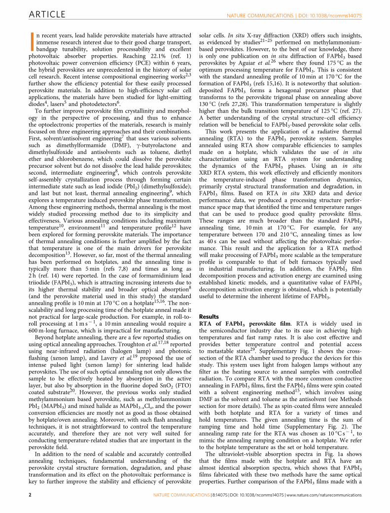
Processing phase space. To gain further insight into processingtime and temperature, we have mapped a more comprehensivepicture of processing phase space and corresponding deviceperformance. To investigate the phase space of the FAPbI3
formation and decomposition, the peak analysis of each of thesamples (as shown in Fig. 2c–e) was used to determine the timeand temperature at which a phase appears or disappears. Thedetails of how this was determined are discussed in the in situXRD data collection and analysis subsection of the Methodssection. The conversion zone diagram is shown in SupplementaryFig. 6, which summarizes our temperature-time experiments byplotting the phases observed as a function of sample temperatureat a given time during the annealing ramp. From SupplementaryFig. 6, zones of conversion are apparent where there are phasetransformations, that is, conversion zone (from precursor toperovskite) and degradation zone (from perovskite to PbI2).
!"#$%"&'"((
!"#$%"&'"(()(!#"'*&+,-#(
(
!#"'*&+,-#((
!#"'*&+,-#(()(!./ 0(
(
!./ 0(
10
2
3
4
5
6789
100
2
3
4
5
6
350330310290
Set temperature (°C)
270250230210190170150130
0.1 13.4 11.9
11.3 12.6
12.5 9.5
8.2 12.7
14
13
12
11
10
9
8
7
Dev
ice
effic
ency
(%
)
Precursor
Precursorand perovskite
Perovskiteand PbI2
PbI2
12.9 12.6
10.812.7
10.912.4
12.612.4
Perovskite appearsPrecursor disapearsPbI2 appearsPerovskite disapearsDevice efficencyReached set temperature
0.1
Perovskite
Tim
e (s
)
Figure 4 | Processing phase space and relevant photovoltaic performances. The film phase is determined from the perovskite appearance
(solid black circles), the precursor disappearance (red diamonds), the PbI2 appearance (blue squares) and the disappearance of the perovskite
(open black circles). The time where the set temperature is reached in the annealing ramp is shown by a pink line. The efficiency data is represented by
triangles.
c
1 µm
1 µm
1.10
1.00
0.90
0.8020
16
12
8
0.80.70.60.50.40.3141210
864
3 4 5 6100
2 3 4 561,000
Annealing time (s)
Voc
(V
)Js
c (m
A c
m–2
)F
FP
CE
(%
)
RTA 170 °C
b
a
Figure 3 | FAPbI3 film morphology and device performance for film
annealed at 170 �C. (a) SEM image (scale bar, 1mm) of FAPbI3 film
annealed at 170 �C for 40 s. (b) SEM image (scale bar, 1mm) of FAPbI3 film
annealed at 170 �C for 5 min. (c) Annealing time dependence of
photovoltaic performance (average, maximum and minimum values show
by the square dots and error bars) for devices with active layer fabricated at
170 �C.
NATURE COMMUNICATIONS | DOI: 10.1038/ncomms14075 ARTICLE
NATURE COMMUNICATIONS | 8:14075 | DOI: 10.1038/ncomms14075 | www.nature.com/naturecommunications 5
With Supplementary Fig. 6, we can calculate the processingphase space diagram. This is shown in Fig. 4 and plots thefilm phase as a function of annealing time verses set temperaturefor samples processed using RTA. The different coloured regionsshow the time-set temperature where the hexagonal FAPbI3
(precursor), trigonal FAPbI3 (perovskite) and PbI2 form, aswell as regions of phase coexistence. The hotplate annealedversion of this figure is plotted in Supplementary Fig. 7.Presenting the data this way makes it possible to overlay thedevice efficiency data on the same graph as the crystal phase data.Efficiency data for samples made with equivalent temperatureprofiles was measured for a set of 18 sample conditions, andthe average efficiency is plotted for each condition in Fig. 4. FromFig. 4 it is possible to identify optimal anneal times for a given settemperature to maximize the FAPbI3 cell efficiency. Vertical cutsin Fig. 4 represent the phase evolution with time for a given settemperature (with a ramp rate of 10 �C s� 1) and so informthe optimal time to anneal a sample to produce the desired crystalstructure. The overlay of the device efficiency (given by thetriangles) and the diffraction data shows that the samples with thebest performance are in the region were the perovskite isfully formed (the light grey region) but a significant amount ofPbI2 has not yet formed (not too far into the orange region).The information in Fig. 4 thus informs further optimization ofthe annealing step in the perovskite synthesis. Not only is thisuseful for achieving good efficiency, but it also informs the useof lower anneal times reducing the thermal load and so reducingthe cost of material manufacturing.
FAPbI3 decomposition kinetics. Radiative annealing with in situX-ray experiments and resulting processing space as discussedin the previous sections suggest FAPbI3 decomposition to PbI2 isa slow, thermally driven transformation. To better understand thekinetics of this transformation process, we quantitatively evaluatethe experimental data with well-developed kinetic models34.Previously, Moore et al.23 have studied crystallization kineticsof CH3NH3PbX3, where X represents lead salts such aschloride, iodide, nitride and acetate, and the proposed Johnson–Mehl–Avrami (JMA) modeling of CH3NH3PbX3 crystallizationcan reveal important details of the perovskite formation.
Here, the kinetics of FAPbI3 decomposition by applyingthe JMA model to our radiative annealing with in situ XRD datais explored. To mathematically perform a materials’ phasetransformation kinetic modelling, a reliable transformationalfraction parameter needs to be identified and traced. ThePbI2 XRD peak area, which is from FAPbI3 decomposition, was
chosen as the transformational parameter fraction and noted asx(t). Following the study by Moore et al.23 leads to kineticequations:
lnðtx2� tx1Þ ¼Ea
RT� ln k0þ lnðbx2�bx1Þ ð1Þ
xðtÞ ¼ 1� exp � k0 exp�Ea
RT
� �t
� �n� �ð2Þ
where tx1 and tx2 are the time at which the transformed fractionis x1 and x2, Ea is the effective activation energy, R is thegas constant, T is the temperature, k0 represents the rate constantprefactor, n is the growth constant and bxn is a state property thatis independent of time/temperature variables. More detailedinformation regarding the derivations and explanationof the equations can be found in the study by Moore et al.23
and kinetic modelling review by Liu et al.34. Figure 5a shows afitted x(t) for isothermally annealing at 210 �C (green, diamond),230 �C (blue, triangle) and 250 �C (red, circle). Applyingequation (1), Fig. 5b shows the extraction of effective activationenergy of decomposition FAPbI3, which is found to be96.5±13.1 kJ mol� 1. This may find use in lifetime predictionsfor FAPbI3 solar cells. Fitting the Fig. 5a data into the JMA model,shown in equation (2), the kinetic reaction prefactork0¼ 1.82� 107±1.28� 105 and the growth constant n is closeto 2 at 210 �C and approaches 3 at 250 �C. This growth constantdependence on the temperature suggests the growth of thedecomposition product (PbI2) is roughly three-dimensionalat higher temperature and two-dimensional (2D) at lowertemperature. Applying the JMA model to the halide perovskitedecomposition system allows for determination of the FAPbI3
decomposition activation energy and decomposition dimension,offering quantitative evaluation of the perovskite kinetics.
DiscussionIn this work we show that processing FAPbI3 usingRTA produces devices with comparable efficiencies to thosemade on a hotplate. We determined the processing phase spaceof FAPbI3 with in situ XRD using an in-house-designed RTA andidentified time and temperature ranges that can be usedto produce good quality films; these are broader than thestandard FAPbI3 annealing conditions. The JMA kinetic modelwas applied to the halide perovskite decomposition process(into PbI2), and the decomposition activation energy isdetermined, which will be useful in determining the inherentlifetime of FAPbI3. This work is promising for the adaptability ofindustrial production of FAPbI3, opening up the potential of
1.0
0.8
0.6
0.4
0.2
0.04 5 6 7 8 9
1002 3 4 5 6 7 8 9
Time (s)
k0 = 1.82 × 10⁷ ± 1.28 × 10⁵
n = 2.5 ± 0.4
250 °C230 °C210 °C
6.5
6.0
5.5
5.0
4.5
4.0
ln (
t x2
– t x
1)
250245240235230
106 (RT)–1 (mol J–1)
Ea = 96.5 ± 13.1 kJ mol–1
b
x (t
)
a
Figure 5 | FAPbI3 decomposition and kinetic modelling. (a) Transformation fraction x(t) as a function of time extracted from isothermal RTA with in situ
XRD data at 210 �C (green, diamond), 230 �C (blue, triangle) and 250 �C (red, circle). Solid lines are fitting results with the JMA model (equation 2).
(b) Reaction time versus inverse temperature from a by fitting equation 1. The error bars are the maximum and minimum values.
ARTICLE NATURE COMMUNICATIONS | DOI: 10.1038/ncomms14075
6 NATURE COMMUNICATIONS | 8:14075 | DOI: 10.1038/ncomms14075 | www.nature.com/naturecommunications

using more rapid ramp rates for processing with fast throughput,such as belt furnaces typically used in manufacturing.
MethodsMaterials. Unless stated otherwise, all materials and solvents were purchasedfrom Sigma-Aldrich and used as received. FAI was from Dyesol. PbI2 (99.999%)was purchased from Alfa Aesar. Spiro-OMeTAD (4 99.5%) was from Lumtec.Fluorine-doped SnO2-coated transparent conducting glass (FTO) was purchasedfrom Thin Film Devices Co.
FAPbI3 film deposition. FAPbI3 perovskite solution was prepared anddeposited as reported by Wozny et al.15, with slight modification. Specifically, a0.7 M stoichiometric FAI and PbI2 in anhydrous DMF solution were prepared,in a glovebox, and stirred for 2 h at room temperature. The resulted clear brightyellow FAPbI3 solution was filtered with 0.20 mm polyvinylidene difluoride filterand spin coated, in a glovebox, on the compact TiO2/FTO substrate by aconsecutive three-step process: 500 r.p.m. for 3 s, 3,500 r.p.m. for 10 s and5,000 r.p.m. for 30 s. One to 2 s before the end of second step, a drop of toluenewas gently place on the spinning substrate to wash off the extra DMF solvent.The resultant transparent film was then placed in a jar, concealed tightly, tookout of the glove box, took out of the jar and annealed in the RTA equipment(Ulvac MILA-3000 Minilamp Annealer). The transfer time from the spin coater tothe RTA is typically 2–5 min. In the XRD experiments, the time between spincoater and RTA is roughly 10–20 min. Once the annealing is done, the annealedfilms were placed back into the jar and transferred to the N2 glove box. For hotplateannealed films, the as spin-coated FAPbI3 films were transferred on the hotplateafter three minutes of waiting to match the RTA film transfer time.
Solar cell fabrication. Pre-patterned FTO glass slides (1� 1 inch) were cleanedwith deionized water and 2-propanol, and ultrasonic bathed in 2-propanal andacetone for 10 min each before performing a 15 min ultraviolet ozone cleaning.A thin (B30 nm) compact TiO2 was deposited on the FTO by spin coating 0.2 Mtitanium diisopropoxide dis(acetylacetonate) (Sigma-Aldrich, 75 wt% in iso-propanol) in 1-butanol (Sigma-Aldrich, 99.8%), with spin coater recipe as700 r.p.m. for 10 s, 1,000 r.p.m. for 10 s and 2,000 r.p.m. for 30 s. The compactTiO2/FTO substrate was then annealed at 500 �C for 1 h. Before depositing theperovskite photoactive layer, the substrates were cleaned with ultraviolet ozone for15 min and transferred into a N2 glove box where a spin coater (Laurell WS-650) isinstalled. The perovskite layer was deposited and processed as stated above. Thehole transporting layer was deposited on the perovskite layer by spin coating, withspin recipe as 3,000 r.p.m. for 30 s, 70ml Spiro-OMeTAD solution, which consistedof 72.3 mg of Spiro OMeTAD dissolved in 1 ml of chlorobenzene, 28.8 ml of4-tert-butylpyridine and 17.5 ml of a bis(trifluoromethanesulfonyl)imide Lithiumsalt (Li-TFSI) solution. The Li-TFSI solution consisted of 520 mg of Li-TFSIdissolved in 1 ml of acetonitrile. The thickness of Spiro-OMeTAD layer wasmeasure to be 100 nm. In the end, the gold electrode was thermally evaporatedon the Spiro-OMeTAD /FAPbI3/compact TiO2/FTO glass with a thicknessof 100 nm.
Photovoltaic characterization. Absorption measurements were taken on aShimadzu UV–vis–NIR 3600 spectrometer at room temperature. SEM images wereobtained using an FEI Nova NanoSEM 630. Solar cell devices were measured underAM1.5 illumination in a N2 glovebox using a solar simulator (Newport, OrielSol3A) calibrated with an National Renewable Energy Laboratory-certifiedSi photodiode (Hamamtsu, S1787-04) equipped with an infrared-cutoff filter(KG3, Schott). A digital source meter (Keithley 2400) is used as external voltageto perform the current J–V characteristics. The devices were light soakedfor 1–1.5 min before performing the J–V scan. The J–V scan rate is 100 mV s� 1
with reverse scan as 1.3 V to -0.2 V and forward scan as � 0.2 V to 1.3 V.A metal aperture of 0.06 cm2 was used when measuring J–V curves.
In situ XRD data collection. The in situ XRD was performed with theRTA chamber described in Ahmad et al.29 using beamline 7-2 at SSRL with aphoton energy of 12 or 12.6 keV (depending on the experiment). The sampletemperature was measured with a sensitive thermocouple that was previouslyshown to be accurate by comparison of the temperature-dependent Ag diffractiondata with the thermocouple35. Lead halide perovskites are beam sensitive and so toavoid significant beam damage, X-ray exposure was limited to 30 s for the durationof the anneal. The duration of 30 s was determined based on the observationthat there was no visible evidence of X-ray damage after this exposure. Additionalevidence that our data collection protocol did not result in beam damage camefrom comparing the XRD from a film exposed to the beam for 30 s to thatfrom a part of the same film but not exposed to X-rays (for example, the samplewas shifted) where there were no noticeable changes in the diffraction pattern.To limit the X-ray exposure to 30 s, 60 scans were taken with a 0.5 s exposure timeand the X-ray beam was closed when the data was not being collected. Toobtain data during the rapid conversion from the precursor to the perovskiteas well as the longer conversion to PbI2 and any grain growth, for longer anneal
times, 30 scans at a shorter interval between scans (1–2 s) was followed by 30 scansat a longer interval depending on the overall scan time (for instance, 30 s in the caseof 15 min annealing). The RTA chamber was purged with N2 for 5–10 min,after loading the as spin-coated films into the chamber, to reduce the O2 andH2O content of the annealing chamber. After purging, RTA from theRTA halogen lamps heated the samples, whereas XRD data were obtainedwhile still flowing N2. The annealing temperature profiles were such that theyovershoot the set temperature by o5 �C and settled to the set temperature.
XRD data analysis. The diffraction was taken using a Pilatus 300k and thedata is converted from 2D to one-dimensional (1D) using WxDiff, code written byMannsfeld36 to convert 2D data to 1D data. Once converted into 1D data, the dataare loaded into IGOR Pro, and selected peaks are fitted using the Multi-peak fitwith a Gaussian peak shape and a linear background. In this way the peak area,FWHM and associated error are extracted for the chosen peaks. The time andtemperature that a phase appears (or disappears) are defined as the average(in time and temp) of the last scan that did not have the peak and the first scan thathas the peak (or vice versa), with the error being half the difference. This isillustrated in Supplementary Fig. 8. The time reported in the time versus settemperature (Fig. 4) and temperature versus time plots (Supplementary Fig. 6)has been corrected such that the t¼ 0 is defined as the time the temperaturereaches 30 �C, to avoid deviations (on the order of r1 s) in the temperatureramp due to differing initial temperatures.
Data availability. The data supporting the findings of this study are availablefrom the corresponding author upon request.
References1. National Renewable Energy Laboratory. Best Research-Cell Efficiencies.
(2016). Available at http://www.nrel.gov/pv/assets/images/efficiency_chart.jpg.Accessed on 10 June 2016.
2. Jeon, N. J. et al. Compositional engineering of perovskite materials forhigh-performance solar cells. Nature 517, 476–480 (2015).
3. Saliba, M. et al. Cesium-containing triple cation perovskite solar cells: improvedstability, reproducibility and high efficiency. Energy Environ. Sci. 9, 1989–1997(2016).
4. Tan, Z.-K. et al. Bright light-emitting diodes based on organometal halideperovskite. Nat. Nanotechnol. 9, 687–692 (2014).
5. Xing, G. et al. Low-temperature solution-processed wavelength-tunableperovskites for lasing. Nat. Mater. 13, 476–480 (2014).
6. Dou, L. et al. Solution-processed hybrid perovskite photodetectors with highdetectivity. Nat. Commun. 5, 5404 (2014).
7. Jeon, N. J. et al. Solvent engineering for high-performance inorganic–organichybrid perovskite solar cells. Nat. Mater. 13, 897–903 (2014).
8. Yang, W. S. et al. High-performance photovoltaic perovskite layers fabricatedthrough intramolecular exchange. Science 348, 1234–1237 (2015).
9. Eperon, G. E. et al. Morphological control for high performance, solution-processed planar heterojunction perovskite solar cells. Adv. Funct. Mater. 24,151–157 (2014).
10. Dualeh, A. et al. Effect of annealing temperature on film morphology oforganic-inorganic hybrid pervoskite solid-state solar cells. Adv. Funct. Mater.24, 3250–3258 (2014).
11. Raga, S. R. et al. Influence of air annealing on high efficiency planar structureperovskite solar cells. Chem. Mater. 27, 1597–1603 (2015).
12. Huang, L. et al. Multi-step slow annealing perovskite films for highperformance planar perovskite solar cells. Sol. Energy Mater. Sol. Cells 141,377–382 (2015).
13. Nenon, D. P. et al. Structural and chemical evolution of methylammonium leadhalide perovskites during thermal processing from solution. Energy Environ.Sci. 9, 2072–2082 (2016).
14. Xie, F. X. et al. Vacuum-assisted thermal annealing of CH3 NH3 PbI3
for highly stable and efficient perovskite solar cells. ACS Nano 9, 639–646(2015).
15. Wozny, S. et al. Controlled humidity study on the formation of higherefficiency formamidinium lead triiodide-based solar cells. Chem. Mater. 27,4814–4820 (2015).
16. Eperon, G. E. et al. Formamidinium lead trihalide: a broadly tunableperovskite for efficient planar heterojunction solar cells. Energy Environ. Sci. 7,982 (2014).
17. Troughton, J. et al. Rapid processing of perovskite solar cells in under 2.5seconds. J. Mater. Chem. A 3, 9123–9127 (2015).
18. Troughton, J. et al. Photonic flash-annealing of lead halide perovskite solar cellsin 1 ms. J. Mater. Chem. A 4, 3471–3476 (2016).
19. Lavery, B. W. et al. Intense pulsed light sintering of CH3 NH3 PbI3 solar cells.ACS Appl. Mater. Interfaces 8, 8419–8426 (2016).
20. Hooper, K. et al. Near infrared radiation as a rapid heating technique forTiO 2 films on glass mounted dye-sensitized solar cells. Int. J. Photoenergy2014, 1–8 (2014).
NATURE COMMUNICATIONS | DOI: 10.1038/ncomms14075 ARTICLE
NATURE COMMUNICATIONS | 8:14075 | DOI: 10.1038/ncomms14075 | www.nature.com/naturecommunications 7

21. Unger, E. L. et al. Chloride in lead chloride-derived organo-metal halides forperovskite-absorber solar cells. Chem. Mater. 26, 7158–7165 (2014).
22. Saliba, M. et al. Influence of thermal processing protocol upon thecrystallization and photovoltaic performance of organic–inorganic leadtrihalide perovskites. J. Phys. Chem. C 118, 17171–17177 (2014).
23. Moore, D. T. et al. Crystallization kinetics of organic-inorganic trihalideperovskites and the role of the lead anion in crystal growth. J. Am. Chem. Soc.137, 2350–2358 (2015).
24. Tan, K. W. et al. Thermally induced structural evolution and performance ofmesoporous block copolymer-directed alumina perovskite solar cells. ACSNano 8, 4730–4739 (2014).
25. Barrows, A. T. et al. Monitoring the formation of a CH3 NH3 PbI3- x Clxperovskite during thermal annealing using X-ray scattering. Adv. Funct. Mater.26, 1–9 (2016).
26. Aguiar, J. A. et al. In situ investigation on the formation and metastability offormamidinium lead tri-iodide perovskite solar cells. Energy Environ. Sci. 9,2372–2382 (2016).
27. Binek, A., Hanusch, F. C., Docampo, P. & Bein, T. Stabilization of the trigonalhigh-temperature phase of formamidinium lead iodide. J. Phys. Chem. Lett. 6,1249–1253 (2015).
28. Stoumpos, C. C., Malliakas, C. D. & Kanatzidis, M. G. Semiconducting tin andlead iodide perovskites with organic cations: Phase transitions, high mobilities,and near-infrared photoluminescent properties. Inorg. Chem. 52, 9019–9038(2013).
29. Ahmad, M. I. et al. Rapid thermal processing chamber for in-situ x-raydiffraction. Rev. Sci. Instrum. 86, 13902 (2015).
30. Hanusch, F. C. et al. Efficient planar heterojunction perovskite solar cells basedon formamidinium lead bromide. J. Phys. Chem. Lett. 5, 2791–2795 (2014).
31. Liu, F. et al. Is excess PbI2 beneficial for perovskite solar cell performance? Adv.Energy Mater 6, 1502206 (2016).
32. Chen, Q. et al. Controllable self-induced passivation of hybrid lead iodideperovskites toward high performance solar cells. Nano Lett. 14, 4158–4163 (2014).
33. Roldan-Carmona, C. et al. High efficiency methylammonium lead triiodideperovskite solar cells: the relevance of non-stoichiometric precursors. EnergyEnviron. Sci. 8, 3550–3556 (2015).
34. Liu, F. et al. Analysis of solid state phase transformation kinetics: models andrecipes. Int. Mater. Rev. 52, 193–212 (2007).
35. Fields, J. D. et al. The formation mechanism for printed silver-contacts forsilicon solar cells. Nat. Commun. 7, 11143 (2016).
36. Mannsfeld, S. C. B. WxDiff. Stanford Synchrotron Radiation Light-Source(2009).
AcknowledgementsThis work was funded by the Bridging Research Interactions through collaborating theDevelopment Grants in Energy (BRIDGE) program under the SunShot initiative of the
Department of Energy (DE-EE0005951). The work at the National Renewable EnergyLaboratory was supported by the Department of Energy under Contract NumberDE-AC36-08GO28308 and the work at Stanford Synchrotron Radiation Lightsource wasfunded by the Department of Energy under Contract No. DE-AC02-76SF00515. StanfordSynchrotron Radiation Lightsource at the SLAC National Accelerator Laboratory is anational user facility operated by Stanford University on behalf of the US Department ofEnergy, Office of Basic Energy Sciences. We thank Bart Johnson (SLAC) for assistancewith SSRL beam line 7-2. We thank Dr Z. Li (NREL) for assisting on SEM images,Dr D. Moore (NREL) for discussion on the kinetic modeling and Dr J. Christians (NREL)for helpful discussions.
Author contributionsV.L.P., B.D., M.F.A.M.v.H. and M.F.T. conceived and designed the study. B.D. fabricatedand characterized all the devices. T.R.K.-S. assisted on device RTA. M.F.A.M.v.H. andB.D. prepared the films for the X-ray experiment. V.L.P., B.D. and M.F.A.M.v.H. con-ducted the X-ray experiments. V.L.P. analysed the XRD data. B.D. performed the kineticmodelling. M.F.A.M.v.H. and M.F.T. directed the project. B.D. and V.L.P. wrote themanuscript and all authors discussed, revised and approved the manuscript.
Additional informationSupplementary Information accompanies this paper at http://www.nature.com/naturecommunications
Competing financial interests: The authors declare no competing financial interests.
Reprints and permission information is available online at http://npg.nature.com/reprintsandpermissions/
How to cite this article: Pool, V. L. et al. Thermal engineering of FAPbI3 perovskitematerial via radiative thermal annealing and in situ XRD. Nat. Commun. 8, 14075doi: 10.1038/ncomms14075 (2017).
Publisher’s note: Springer Nature remains neutral with regard to jurisdictional claims inpublished maps and institutional affiliations.
This work is licensed under a Creative Commons Attribution 4.0International License. The images or other third party material in this
article are included in the article’s Creative Commons license, unless indicated otherwisein the credit line; if the material is not included under the Creative Commons license,users will need to obtain permission from the license holder to reproduce the material.To view a copy of this license, visit http://creativecommons.org/licenses/by/4.0/
r The Author(s) 2017
ARTICLE NATURE COMMUNICATIONS | DOI: 10.1038/ncomms14075
8 NATURE COMMUNICATIONS | 8:14075 | DOI: 10.1038/ncomms14075 | www.nature.com/naturecommunications