Embed Size (px)
Citation preview
July 2013 Page 1 of 13
Thermal Management of Light Sources Based on SMD LEDs
Application note
Abstract
This application note provides an introduction to the basic principles of heat transfer and its influence on LED applications using thermal management at different system levels. It describes and discusses relevant characteristics.
Introduction
Light-emitting diodes (LEDs) are used and accepted in many areas of lighting technology today. They are light sources of the future, and already represent the latest state of technology for many applications. Thanks to the direct conversion of electrical current to light (optical radiation) in the semiconductor, LEDs are highly efficient – more efficient than most traditional light sources. However, even in the case of LEDs, nearly most of the electrical power is converted to heat rather than light. To put it simply, the higher the current, the more heat is created in the component. This heat loss must be conducted away from the LEDs, since the used semiconductor material is subject to a maximum temperature limit and because its characteristic properties such as forward voltage, wave length, and service life may vary with the temperature. In particular in the case of innovative, miniaturized high-performance LEDs, the dissipation of heat is centrally important in order to keep temperatures down – and is regarded as the biggest challenge. Only adequate thermal management across all system levels can allow the full exploitation of LED performance and efficiency during operation.
This paper provides a general introduction to the basic principles of heat transfer and its influence on LED applications using thermal management at different system levels. Relevant characteristics are described and discussed in this context.
Basic principles of heat transfer
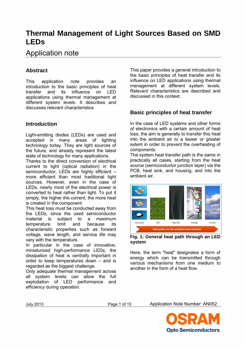
In the case of LED systems and other forms of electronics with a certain amount of heat loss, the aim is generally to transfer this heat into the ambient air to a lesser or greater extent in order to prevent the overheating of components. The system heat transfer path is the same in practically all cases, starting from the heat source (semiconductor junction layer) via the PCB, heat sink, and housing, and into the ambient air.
Fig. 1: General heat path through an LED system
Here, the term "heat" designates a form of energy which can be transmitted through various mechanisms from one medium to another in the form of a heat flow.
Application Note Number: AN052
July 2013 Page 2 of 13
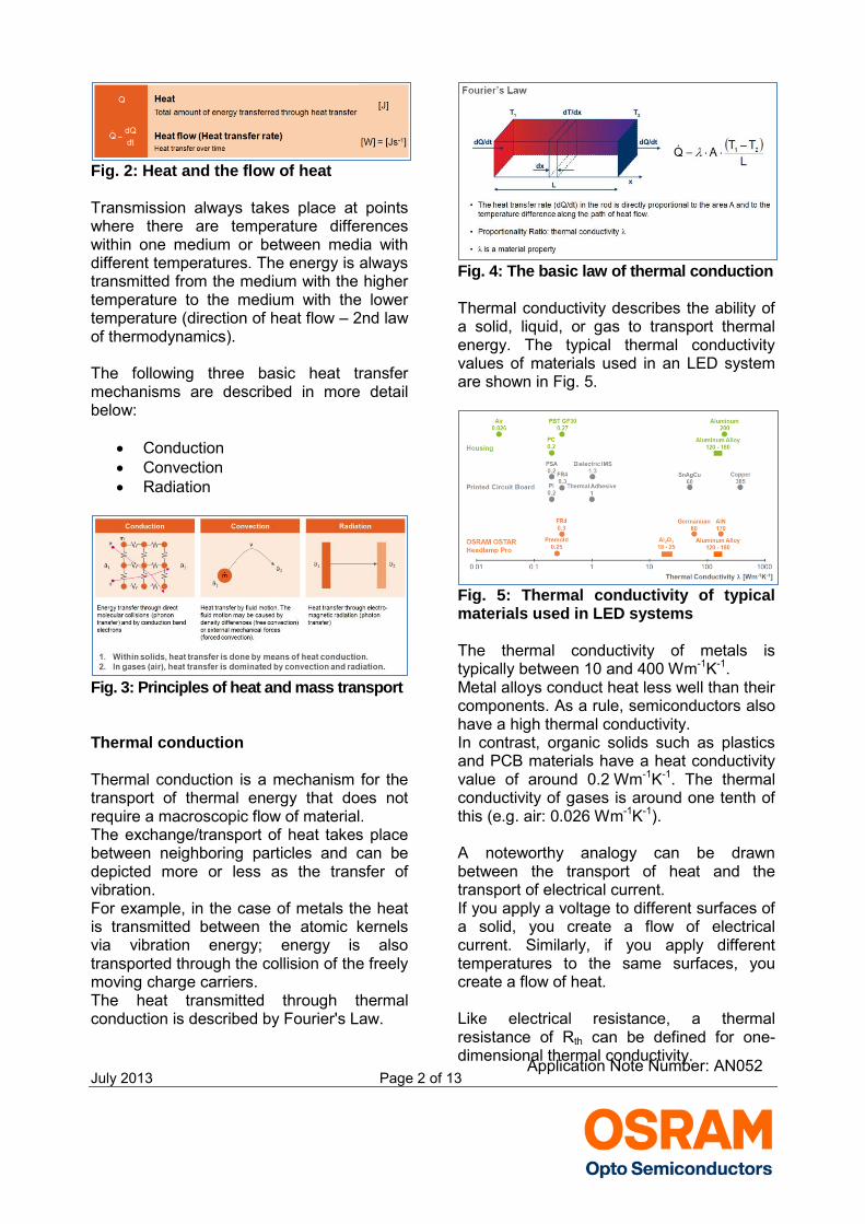
Fig. 2: Heat and the flow of heat Transmission always takes place at points where there are temperature differences within one medium or between media with different temperatures. The energy is always transmitted from the medium with the higher temperature to the medium with the lower temperature (direction of heat flow – 2nd law of thermodynamics). The following three basic heat transfer mechanisms are described in more detail below:
Conduction Convection Radiation
Fig. 3: Principles of heat and mass transport Thermal conduction Thermal conduction is a mechanism for the transport of thermal energy that does not require a macroscopic flow of material. The exchange/transport of heat takes place between neighboring particles and can be depicted more or less as the transfer of vibration. For example, in the case of metals the heat is transmitted between the atomic kernels via vibration energy; energy is also transported through the collision of the freely moving charge carriers. The heat transmitted through thermal conduction is described by Fourier's Law.
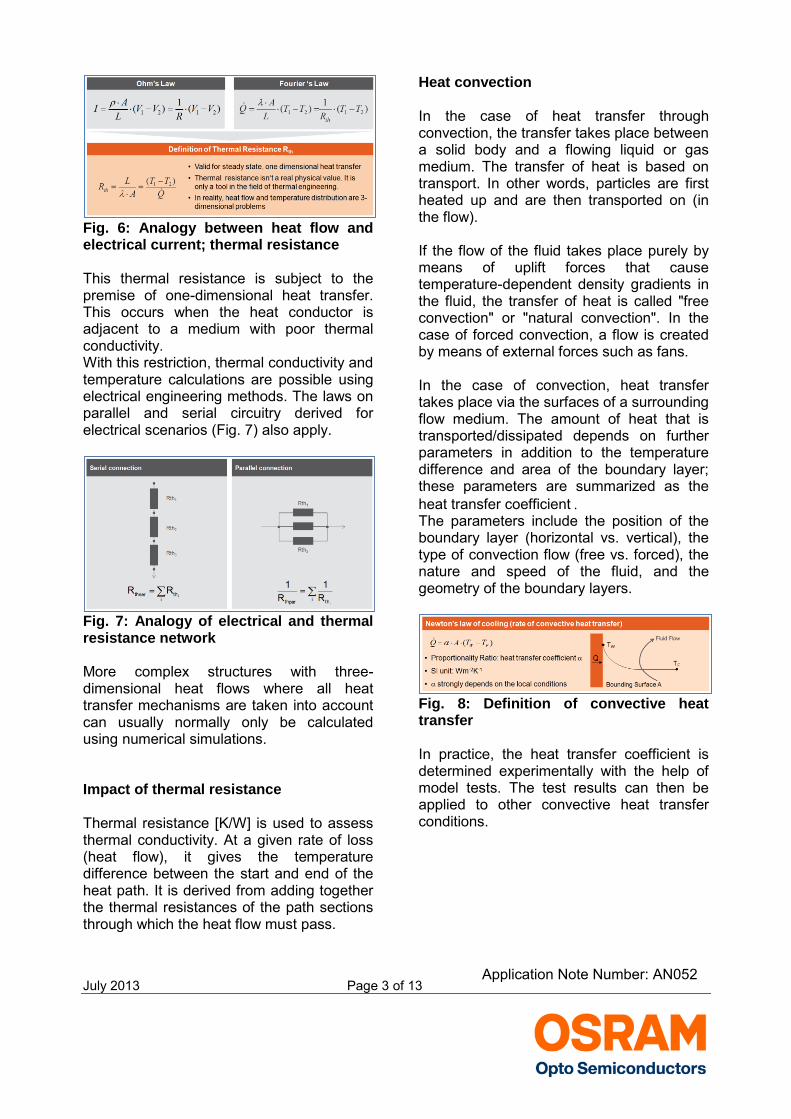
Fig. 4: The basic law of thermal conduction Thermal conductivity describes the ability of a solid, liquid, or gas to transport thermal energy. The typical thermal conductivity values of materials used in an LED system are shown in Fig. 5.
Fig. 5: Thermal conductivity of typical materials used in LED systems The thermal conductivity of metals is typically between 10 and 400 Wm-1K-1. Metal alloys conduct heat less well than their components. As a rule, semiconductors also have a high thermal conductivity. In contrast, organic solids such as plastics and PCB materials have a heat conductivity value of around 0.2 Wm-1K-1. The thermal conductivity of gases is around one tenth of this (e.g. air: 0.026 Wm-1K-1). A noteworthy analogy can be drawn between the transport of heat and the transport of electrical current. If you apply a voltage to different surfaces of a solid, you create a flow of electrical current. Similarly, if you apply different temperatures to the same surfaces, you create a flow of heat. Like electrical resistance, a thermal resistance of Rth can be defined for one-dimensional thermal conductivity. Application Note Number: AN052
July 2013 Page 3 of 13
Fig. 6: Analogy between heat flow and electrical current; thermal resistance This thermal resistance is subject to the premise of one-dimensional heat transfer. This occurs when the heat conductor is adjacent to a medium with poor thermal conductivity. With this restriction, thermal conductivity and temperature calculations are possible using electrical engineering methods. The laws on parallel and serial circuitry derived for electrical scenarios (Fig. 7) also apply.
Fig. 7: Analogy of electrical and thermal resistance network More complex structures with three-dimensional heat flows where all heat transfer mechanisms are taken into account can usually normally only be calculated using numerical simulations. Impact of thermal resistance Thermal resistance [K/W] is used to assess thermal conductivity. At a given rate of loss (heat flow), it gives the temperature difference between the start and end of the heat path. It is derived from adding together the thermal resistances of the path sections through which the heat flow must pass.
Heat convection In the case of heat transfer through convection, the transfer takes place between a solid body and a flowing liquid or gas medium. The transfer of heat is based on transport. In other words, particles are first heated up and are then transported on (in the flow). If the flow of the fluid takes place purely by means of uplift forces that cause temperature-dependent density gradients in the fluid, the transfer of heat is called "free convection" or "natural convection". In the case of forced convection, a flow is created by means of external forces such as fans. In the case of convection, heat transfer takes place via the surfaces of a surrounding flow medium. The amount of heat that is transported/dissipated depends on further parameters in addition to the temperature difference and area of the boundary layer; these parameters are summarized as the heat transfer coefficient The parameters include the position of the boundary layer (horizontal vs. vertical), the type of convection flow (free vs. forced), the nature and speed of the fluid, and the geometry of the boundary layers.
Fig. 8: Definition of convective heat transfer In practice, the heat transfer coefficient is determined experimentally with the help of model tests. The test results can then be applied to other convective heat transfer conditions.
Application Note Number: AN052
July 2013 Page 4 of 13
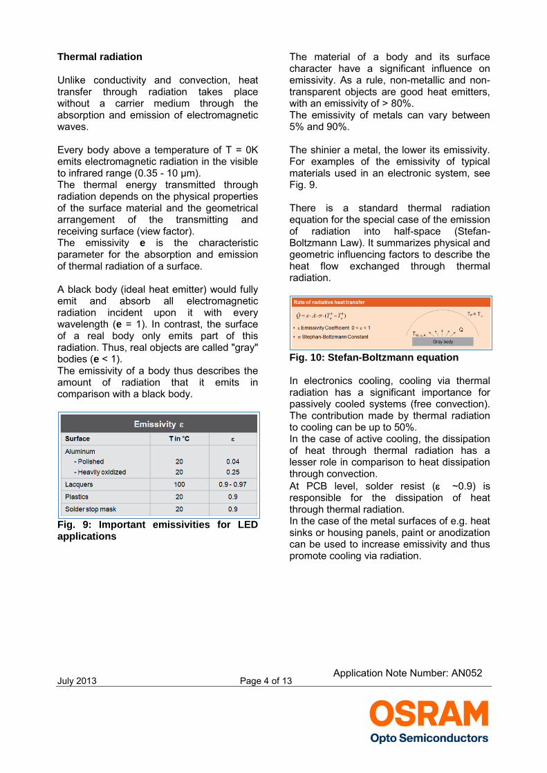
Thermal radiation Unlike conductivity and convection, heat transfer through radiation takes place without a carrier medium through the absorption and emission of electromagnetic waves. Every body above a temperature of T = 0K emits electromagnetic radiation in the visible to infrared range (0.35 - 10 µm). The thermal energy transmitted through radiation depends on the physical properties of the surface material and the geometrical arrangement of the transmitting and receiving surface (view factor). The emissivity e is the characteristic parameter for the absorption and emission of thermal radiation of a surface. A black body (ideal heat emitter) would fully emit and absorb all electromagnetic radiation incident upon it with every wavelength (e = 1). In contrast, the surface of a real body only emits part of this radiation. Thus, real objects are called "gray" bodies (e < 1). The emissivity of a body thus describes the amount of radiation that it emits in comparison with a black body.
Fig. 9: Important emissivities for LED applications
The material of a body and its surface character have a significant influence on emissivity. As a rule, non-metallic and non-transparent objects are good heat emitters, with an emissivity of > 80%. The emissivity of metals can vary between 5% and 90%. The shinier a metal, the lower its emissivity. For examples of the emissivity of typical materials used in an electronic system, see Fig. 9. There is a standard thermal radiation equation for the special case of the emission of radiation into half-space (Stefan-Boltzmann Law). It summarizes physical and geometric influencing factors to describe the heat flow exchanged through thermal radiation.
Fig. 10: Stefan-Boltzmann equation In electronics cooling, cooling via thermal radiation has a significant importance for passively cooled systems (free convection). The contribution made by thermal radiation to cooling can be up to 50%. In the case of active cooling, the dissipation of heat through thermal radiation has a lesser role in comparison to heat dissipation through convection. At PCB level, solder resist ( ~0.9) is responsible for the dissipation of heat through thermal radiation. In the case of the metal surfaces of e.g. heat sinks or housing panels, paint or anodization can be used to increase emissivity and thus promote cooling via radiation.
Application Note Number: AN052
July 2013 Page 5 of 13
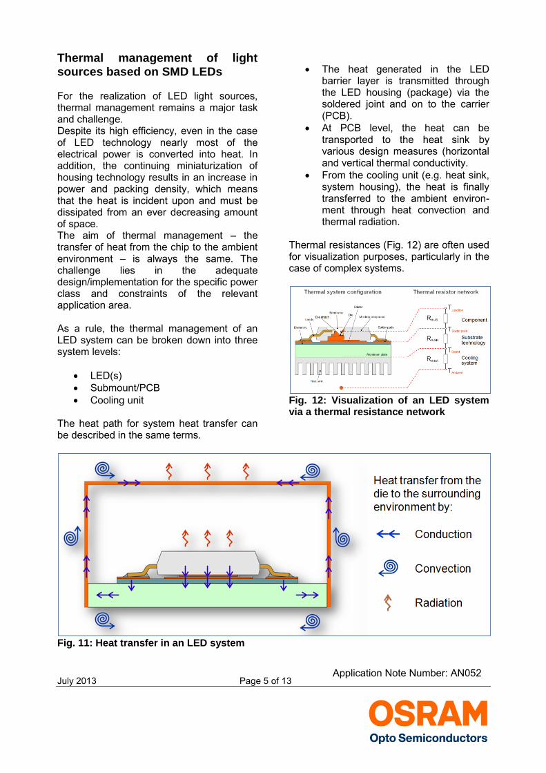
Thermal management of light sources based on SMD LEDs For the realization of LED light sources, thermal management remains a major task and challenge. Despite its high efficiency, even in the case of LED technology nearly most of the electrical power is converted into heat. In addition, the continuing miniaturization of housing technology results in an increase in power and packing density, which means that the heat is incident upon and must be dissipated from an ever decreasing amount of space. The aim of thermal management – the transfer of heat from the chip to the ambient environment – is always the same. The challenge lies in the adequate design/implementation for the specific power class and constraints of the relevant application area. As a rule, the thermal management of an LED system can be broken down into three system levels:
LED(s) Submount/PCB Cooling unit
The heat path for system heat transfer can be described in the same terms.
The heat generated in the LED
barrier layer is transmitted through the LED housing (package) via the soldered joint and on to the carrier (PCB).
At PCB level, the heat can be transported to the heat sink by various design measures (horizontal and vertical thermal conductivity.
From the cooling unit (e.g. heat sink, system housing), the heat is finally transferred to the ambient environ-ment through heat convection and thermal radiation.
Thermal resistances (Fig. 12) are often used for visualization purposes, particularly in the case of complex systems.
Fig. 12: Visualization of an LED system via a thermal resistance network
Fig. 11: Heat transfer in an LED system
Application Note Number: AN052
July 2013 Page 6 of 13
The thermal partial resistances correspond to the various functional groups in the system or heat path and characterize their individual thermal behavior.
Rth JS is the thermal resistance of the LED and describes the transfer of heat within the LED housing (junction-to-solder-point);
Rth SB is the thermal resistance of the PCB technology (solder-point-to-board);
Rth BA is the thermal resistance of the
transfer of heat into the ambient environment (board-to-ambient).
Thermal management at LED level At LED level, thermal management is generally predefined by the component manufacturer and is determined by the design of the LED. The thermal resistance of an LED tells us about its thermal properties. This thermal resistance is usually stated on the LED data sheet as a characteristic parameter. As a general rule, the smaller the thermal resistance of an LED, the faster the heat can be dissipated from the housing. Significant influencing factors on thermal resistance include the technology used for the housing and the light-emitting semiconductor chip. In general, the SMD LEDs available at OSRAM Opto Semiconductors can be divided into two groups:
Lead-frame-based LED housings Ceramic-based LED housings
Although the thermal properties of an LED are fixed, knowledge of the heat path of the LED is decisive for the thermal design of the PCB and system.
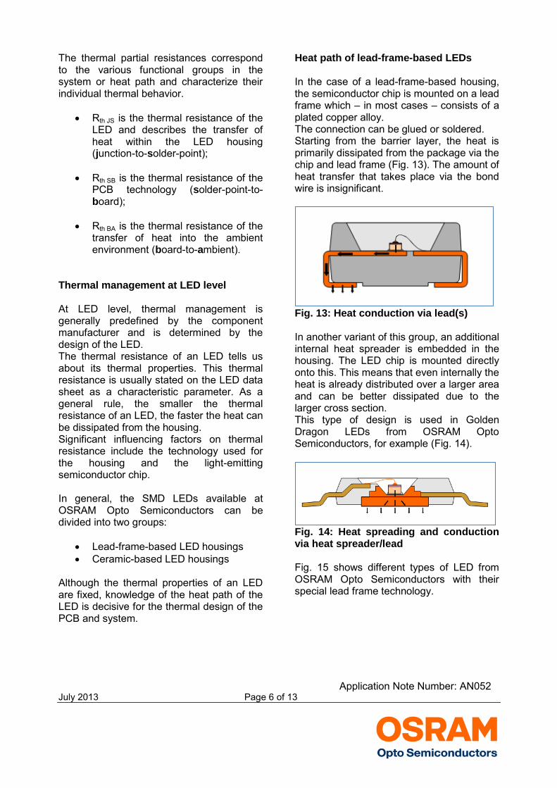
Heat path of lead-frame-based LEDs In the case of a lead-frame-based housing, the semiconductor chip is mounted on a lead frame which – in most cases – consists of a plated copper alloy. The connection can be glued or soldered. Starting from the barrier layer, the heat is primarily dissipated from the package via the chip and lead frame (Fig. 13). The amount of heat transfer that takes place via the bond wire is insignificant.
Fig. 13: Heat conduction via lead(s) In another variant of this group, an additional internal heat spreader is embedded in the housing. The LED chip is mounted directly onto this. This means that even internally the heat is already distributed over a larger area and can be better dissipated due to the larger cross section. This type of design is used in Golden Dragon LEDs from OSRAM Opto Semiconductors, for example (Fig. 14).
Fig. 14: Heat spreading and conduction via heat spreader/lead Fig. 15 shows different types of LED from OSRAM Opto Semiconductors with their special lead frame technology.
Application Note Number: AN052
July 2013 Page 7 of 13
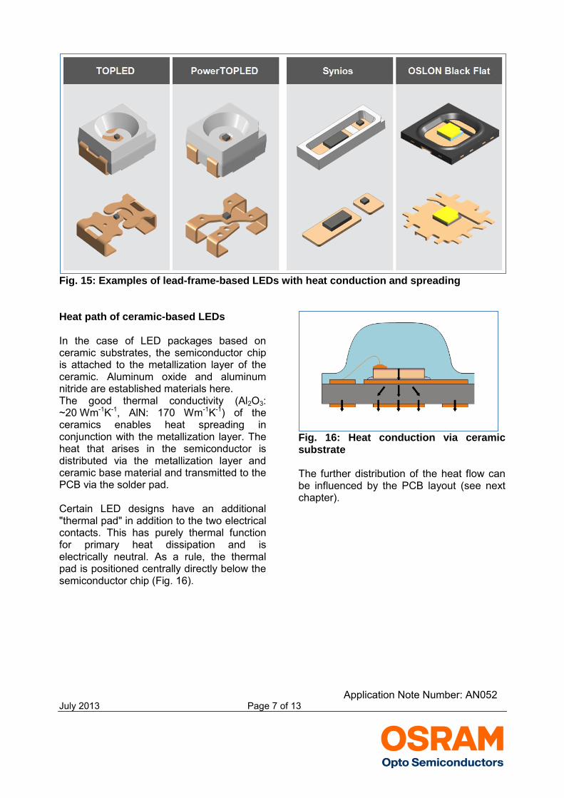
Fig. 15: Examples of lead-frame-based LEDs with heat conduction and spreading Heat path of ceramic-based LEDs In the case of LED packages based on ceramic substrates, the semiconductor chip is attached to the metallization layer of the ceramic. Aluminum oxide and aluminum nitride are established materials here. The good thermal conductivity (Al2O3: ~20 Wm-1K-1, AlN: 170 Wm-1K-1) of the ceramics enables heat spreading in conjunction with the metallization layer. The heat that arises in the semiconductor is distributed via the metallization layer and ceramic base material and transmitted to the PCB via the solder pad. Certain LED designs have an additional "thermal pad" in addition to the two electrical contacts. This has purely thermal function for primary heat dissipation and is electrically neutral. As a rule, the thermal pad is positioned centrally directly below the semiconductor chip (Fig. 16).
Fig. 16: Heat conduction via ceramic substrate The further distribution of the heat flow can be influenced by the PCB layout (see next chapter).
Application Note Number: AN052
July 2013 Page 8 of 13
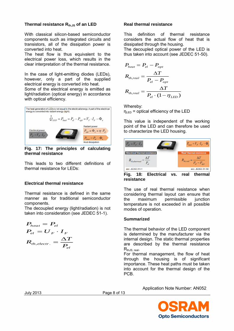
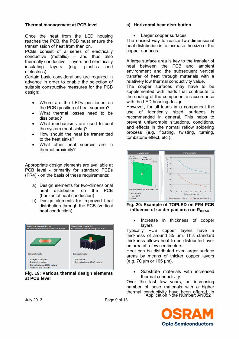
Thermal resistance Rth,JS of an LED With classical silicon-based semiconductor components such as integrated circuits and transistors, all of the dissipation power is converted into heat. The heat flow is thus equivalent to the electrical power loss, which results in the clear interpretation of the thermal resistance. In the case of light-emitting diodes (LEDs), however, only a part of the supplied electrical energy is converted into heat. Some of the electrical energy is emitted as light/radiation (optical energy) in accordance with optical efficiency.
Fig. 17: The principles of calculating thermal resistance This leads to two different definitions of thermal resistance for LEDs: Electrical thermal resistance Thermal resistance is defined in the same manner as for traditional semiconductor components. The decoupled energy (light/radiation) is not taken into consideration (see JEDEC 51-1).
el
electrth
FFel
elheat
P
TR
IUP
PP
.,
Real thermal resistance This definition of thermal resistance considers the actual flow of heat that is dissipated through the housing. The decoupled optical power of the LED is thus taken into account (see JEDEC 51-50).
)1(,
,
LEDel
realth
optel
realth
optelheat
P
TR
PP
TR
PPP
Whereby: ηLED = optical efficiency of the LED This value is independent of the working point of the LED and can therefore be used to characterize the LED housing.
Fig. 18: Electrical vs. real thermal resistance
The use of real thermal resistance when considering thermal layout can ensure that the maximum permissible junction temperature is not exceeded in all possible modes of operation. Summarized The thermal behavior of the LED component is determined by the manufacturer via the internal design. The static thermal properties are described by the thermal resistance RthJS, real. For thermal management, the flow of heat through the housing is of significant importance. These heat paths must be taken into account for the thermal design of the PCB.
Application Note Number: AN052
July 2013 Page 9 of 13
Thermal management at PCB level
Once the heat from the LED housing reaches the PCB, the PCB must ensure the transmission of heat from then on. PCBs consist of a series of electrically conductive (metallic) – and thus also thermally conductive – layers and electrically insulating layers (e.g. plastics and dielectrics). Certain basic considerations are required in advance in order to enable the selection of suitable constructive measures for the PCB design:
Where are the LEDs positioned on the PCB (position of heat sources)?
What thermal losses need to be dissipated?
What mechanisms are used to cool the system (heat sinks)?
How should the heat be transmitted to the heat sinks?
What other heat sources are in thermal proximity?
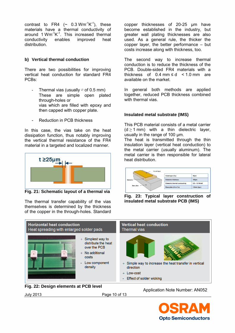
Appropriate design elements are available at PCB level - primarily for standard PCBs (FR4) - on the basis of these requirements:
a) Design elements for two-dimensional heat distribution on the PCB (horizontal heat conduction)
b) Design elements for improved heat distribution through the PCB (vertical heat conduction)
Fig. 19: Various thermal design elements at PCB level
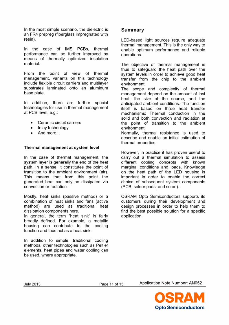
a) Horizontal heat distribution
Larger copper surfaces The easiest way to realize two-dimensional heat distribution is to increase the size of the copper surfaces. A large surface area is key to the transfer of heat between the PCB and ambient environment and the subsequent vertical transfer of heat through materials with a relatively low thermal conductivity value. The copper surfaces may have to be supplemented with leads that contribute to the cooling of the component in accordance with the LED housing design. However, for all leads in a component the use of identically sized surfaces is recommended in general. This helps to prevent unfavorable situations, conditions, and effects in the normal reflow soldering process (e.g. floating, twisting, turning, tombstone effect, etc.).
Fig. 20: Example of TOPLED on FR4 PCB – influence of solder pad area on Rth,PCB
Increase in thickness of copper layers
Typically PCB copper layers have a thickness of around 35 µm. This standard thickness allows heat to be distributed over an area of a few centimeters. Heat can be distributed over larger surface areas by means of thicker copper layers (e.g. 70 µm or 105 µm).
Substrate materials with increased thermal conductivity
Over the last few years, an increasing number of base materials with a higher thermal conductivity have been offered. In
Application Note Number: AN052
July 2013 Page 10 of 13
contrast to FR4 (~ 0.3 Wm-1K-1), these materials have a thermal conductivity of around 1 Wm-1K-1. This increased thermal conductivity enables improved heat distribution. b) Vertical thermal conduction There are two possibilities for improving vertical heat conduction for standard FR4 PCBs:
- Thermal vias (usually ∅ of 0.5 mm)
These are simple open plated through-holes or vias which are filled with epoxy and then capped with copper plate.
- Reduction in PCB thickness In this case, the vias take on the heat dissipation function, thus notably improving the vertical thermal resistance of the FR4 material in a targeted and localized manner.
Fig. 21: Schematic layout of a thermal via The thermal transfer capability of the vias themselves is determined by the thickness of the copper in the through-holes. Standard
copper thicknesses of 20-25 µm have become established in the industry, but greater wall plating thicknesses are also used. As a general rule, the thicker the copper layer, the better performance – but costs increase along with thickness, too. The second way to increase thermal conduction is to reduce the thickness of the PCB. Double-sided FR4 materials with a thickness of 0.4 mm ≤ d < 1.0 mm are available on the market. In general both methods are applied together, reduced PCB thickness combined with thermal vias. Insulated metal substrate (IMS) This PCB material consists of a metal carrier (d ≥ 1 mm) with a thin dielectric layer, usually in the range of 100 µm. The heat is transmitted through the thin insulation layer (vertical heat conduction) to the metal carrier (usually aluminum). The metal carrier is then responsible for lateral heat distribution.
Fig. 23: Typical layer construction of insulated metal substrate PCB (IMS)
Fig. 22: Design elements at PCB level
Application Note Number: AN052
July 2013 Page 11 of 13
In the most simple scenario, the dielectric is an FR4 prepreg (fiberglass impregnated with resin). In the case of IMS PCBs, thermal performance can be further improved by means of thermally optimized insulation material. From the point of view of thermal management, variants on this technology include flexible circuit carriers and multilayer substrates laminated onto an aluminum base plate. In addition, there are further special technologies for use in thermal management at PCB level, e.g.:
Ceramic circuit carriers Inlay technology And more...
Thermal management at system level In the case of thermal management, the system layer is generally the end of the heat path. In a sense, it constitutes the point of transition to the ambient environment (air). This means that from this point the generated heat can only be dissipated via convection or radiation. Mostly, heat sinks (passive method) or a combination of heat sinks and fans (active method) are used as traditional heat dissipation components here. In general, the term "heat sink" is fairly broadly defined. For example, a metallic housing can contribute to the cooling function and thus act as a heat sink. In addition to simple, traditional cooling methods, other technologies such as Peltier elements, heat pipes and water cooling can be used, where appropriate.
Summary LED-based light sources require adequate thermal management. This is the only way to enable optimum performance and reliable operations. The objective of thermal management is thus to safeguard the heat path over the system levels in order to achieve good heat transfer from the chip to the ambient environment. The scope and complexity of thermal management depend on the amount of lost heat, the size of the source, and the anticipated ambient conditions. The function itself is based on three heat transfer mechanisms: Thermal conduction in the solid and both convection and radiation at the point of transition to the ambient environment. Normally, thermal resistance is used to describe and enable an initial estimation of thermal properties. However, in practice it has proven useful to carry out a thermal simulation to assess different cooling concepts with known marginal conditions and loads. Knowledge on the heat path of the LED housing is important in order to enable the correct choice of subsequent system components (PCB, solder pads, and so on). OSRAM Opto Semiconductors supports its customers during their development and design processes in order to help them to find the best possible solution for a specific application.
Application Note Number: AN052
July 2013 Page 12 of 13
Appendix
Do not forget: ledlightforyou.com is the place to go whenever you need information and a list of worldwide partners for your LED lighting projects:
www.ledlightforyou.com Authors: Rainer Huber, Andreas Stich ABOUT OSRAM OPTO SEMICONDUCTORS OSRAM, Munich, Germany is one of the two leading light manufacturers in the world. Its subsidiary, OSRAM Opto Semiconductors GmbH in Regensburg (Germany), offers its customers solutions based on semiconductor technology for lighting, sensor and visualization applications. Osram Opto Semiconductors has production sites in Regensburg (Germany), Penang (Malaysia) and Wuxi (China). Its headquarters for North America is in Sunnyvale (USA), and for Asia in Hong Kong. Osram Opto Semiconductors also has sales offices throughout the world. For more information go to www.osram-os.com. DISCLAIMER PLEASE CAREFULLY READ THE BELOW TERMS AND CONDITIONS BEFORE USING THE INFORMATION SHOWN HEREIN. IF YOU DO NOT AGREE WITH ANY OF THESE TERMS AND CONDITIONS, DO NOT USE THE INFORMATION. The information shown in this document is provided by OSRAM Opto Semiconductors GmbH on an “as is basis” and without OSRAM Opto Semiconductors GmbH assuming, express or implied, any warranty or liability whatsoever, including, but not limited to the warranties of correctness, completeness, merchantability, fitness for a particular purpose, title or non-infringement of rights. In no event shall OSRAM Opto Semiconductors GmbH be liable - regardless of the legal theory - for any direct, indirect, special, incidental, exemplary, consequential, or punitive damages related to the use of the information. This limitation shall apply even if OSRAM Opto Semiconductors GmbH has been advised of possible damages. As some jurisdictions do not allow the exclusion of certain warranties or limitations of liability, the above limitations or exclusions might not apply. The liability of OSRAM Opto Semiconductors GmbH would in such case be limited to the greatest extent permitted by law.
Application Note Number: AN052
July 2013 Page 13 of 13
OSRAM Opto Semiconductors GmbH may change the information shown herein at anytime without notice to users and is not obligated to provide any maintenance (including updates or notifications upon changes) or support related to the information. Any rights not expressly granted herein are reserved. Except for the right to use the information shown herein, no other rights are granted nor shall any obligation be implied requiring the grant of further rights. Any and all rights or licenses for or regarding patents or patent applications are expressly excluded.
Application Note Number: AN052