Embed Size (px)
Citation preview

THERMAL METROLOGY TECHNIQUES FOR ULTRAVIOLET
LIGHT EMITTING DIODES
A Thesis
Presented to
The Academic Faculty
by
Shweta Natarajan
In Partial Fulfillment
of the Requirements for the Degree
Master of Science in the
School of Mechanical Engineering
Georgia Institute of Technology
December 2012
Copyright 2012 by Shweta Natarajan

THERMAL METROLOGY TECHNIQUES FOR ULTRAVIOLET
LIGHT EMITTING DIODES
Approved by:
Dr. Samuel Graham, Advisor
School of Mechanical Engineering
Georgia Institute of Technology
Dr. Andrei G. Fedorov
School of Mechanical Engineering
Georgia Institute of Technology
Dr. Shyh-Chiang Shen
School of Electrical and Computer Engineering
Georgia Institute of Technology
Date Approved: October 18th
, 2012

To my parents – Indira and Ram Natarajan, my grandparents – Gowri and
P.K. Murthy, and my husband Ashok Rajendar

i
ACKNOWLEDGEMENTS
I am grateful to my advisor, Prof. Samuel Graham, for his guidance, mentorship, support and
inspiration over the past few years. Prof. Graham taught me to approach a multi-disciplinary
problem from its fundamental roots, and challenged me be a better thinker and a better
researcher. It has truly been an honor to work with him.
I would like to thank Prof. Andrei Fedorov and Prof. Shyh-Chiang Shen for taking the time to
be on my committee. Their guidance is very much appreciated.
I would like to thank Prof. Timothy Lieuwen and Dr. Jacqueline O’Connor, for their mentorship
and teachings during my time as an undergraduate researcher. I am very fortunate to have
worked with Jackie - I have learned much from her about solving scientific problems and about
being a successful individual, and for that I am grateful.
I would like to thank my supervisor during my internship at 3M, Dr. Karl Geisler. I could not
have asked for a better mentor. I have learned a lot from him and am truly grateful for his
technical and professional guidance.
I would like to thank Sukwon Choi and Dr. Thomas Beechem for their guidance regarding
Raman spectroscopy. I would also like to thank all members of the Graham group, past and
present, for their support and teachings.
I am extremely grateful to Dr. Wayne Whiteman and Ms. Glenda Johnson for their insights
about graduate school, and their patience with my problems. Their guidance was invaluable.
Over the past few years, I have had the fortune to work with and learn from some truly
wonderful people. I would like to thank my good friend Dr. Anusha Venkatachalam for teaching
me the basics of my research topic, for her support, and for her professional advice. I am very

ii
grateful to my good friend Yishak Habtemichael for his insights into our research, and his
constant cheerful demeanor. I am very grateful to my close friends F. Nazli Donmezer and Dr.
Anuradha Bulusu for their technical and personal advice, and for their emotional support. I am
grateful to Anne Mallow and Dr. Timothy Hsu for being great friends and officemates. These
people really did make graduate school at Georgia Tech a happy experience for me, and I could
not have made it this far without their support and companionship.
I am very grateful to my best friend, Sweta Vajjhala, for always being there for me. She has
taught me the value of true friendship, and I am extremely fortunate to have her in my life.
Lastly, I am grateful beyond words to my family. I truly owe all of successes to my parents,
grandparents, parents-in-law, sister and husband. Their unconditional love and support motivates
me to do better every single day. I cannot thank them enough.

iii
TABLE OF CONTENTS
Page
ACKNOWLEDGEMENTS i
LIST OF TABLES v
LIST OF FIGURES vii
SUMMARY xv
CHAPTER
1 INTRODUCTION AND MOTIVATION 1
1.1 Introduction to UV LEDs 1
1.2 Operating principles of an LED 8
1.3 Fundamental challenges in the development of DUV LEDs 13
1.4 The Flip Chip package structure for high power visible and UV
LEDs 26
1.5 The effect of temperature on UV LED degradation 33
1.6 Research motivation and outline 39
2 UV LED PACKAGING AND LITERATURE REVIEW OF UV LED THERMAL
METROLOGY 42
2.1 Packaging schemes for high power LEDs 42
2.2 Metrology techniques for high power UV LEDs and literature
review of key studies 47
3 EXPERIMENTAL METHODOLOGY FOR INTERNAL DEVICE
TEMPERATURE MEASUREMENTS 74
3.1 Device structure, electrode geometries and measurement locations of
investigated UV LEDs 74
3.2 Instrumentation, calibration and measurement procedures for micro-
Raman spectroscopy 84

iv
3.3 Instrumentation, calibration and measurement procedure for Infrared
spectroscopy 89
3.4 Instrumentation, calibration and measurement procedures for
Electroluminescence (EL) spectroscopy 91
3.5 Calibration and measurement procedures using the Forward Voltage
method 94
4 EXPERIMENTAL RESULTS AND DATA ANALYSIS FOR INTERNAL DEVICE
TEMPERATURE MEASUREMENTS 97
4.1 Experimental results and data analysis for micropixel devices 97
4.2 Experimental results and data analysis for interdigitated devices 127
5 MEASUREMENTS OF THE THERMAL RESISTANCE EXTERNAL TO THE
LED 138
5.1 Modified Thermal Resistance Analysis by Induced Transient
(TRAIT) method 138
5.2 The results of the modified TRAIT method applied to the ANSYS
based FEA of an LED package 149
5.3 The results of the modified TRAIT method applied to the white
light LED with an IMS substrate 154
5.4 The results of the modified TRAIT method applied to the white
light LED with an SMT substrate 158
5.4 The results of the modified TRAIT method applied to the yellow
light LED 162
6 CONCLUSIONS AND FUTURE WORK 166
APPENDIX A 170
APPENDIX B 173
APPENDIX C 176
REFERENCES 177

v
LIST OF TABLES
Page
Table 3.1 Table describing the four micropixel UV LED devices investigated in this
study 77
Table 4.1 Stokes peak shift coefficients from Eq. 2.6 for Locations II and III, in a
micropixel without a hotspot, in the DUVL device, as well as the
coefficient of determination of fit for Eq. 2.6 101
Table 4.2 Peak shift coefficients from Eq. 2.6, and coefficients of linear fit in the
correction for inverse piezoelectric stress in Eq. 3.2, as well as the
coefficients of determination for Eqs. 2.6 and 3.2, for Location I for the
micropixel without the hotspot, in the DUVL device 101
Table 4.3 Linewidth method coefficients of fit, from Eq. 3.9, for Locations II and
III, in the micropixel with a hotspot, as well as the coefficient of
determination of fit for Eq. 3.9 109
Table 4.4 Temperature rise at the hotspot, measured by micro-Raman thermography
at Locations II and III, and by IR thermography, at an input power of 400
mW 109
Table 4.5 Micro-Raman peak shift coefficients for the AlN and sapphire layers
(Locations II and III) in the micropixel Devices 1, 2, 3 and 4, from Eq.
2.6, as well as the R2 value of fit 111
Table 4.6 Comparison of temperature measured by EL spectroscopy and micro-
Raman spectroscopy on Location I of the DUVL 121
Table 4.7 Vf method calibration coefficients from Eq. 2.1 for the micropixel devices 124
Table 4.8 Micro-Raman peak shift coefficients from Eq. 2.6 for the AlN and p-GaN
layers in the interdigitated device, along with the R2 of fit 129
Table 5.1 Thermal resistances and capacitances derived from the modified TRAIT
method, for the ANSYS based thermal finite element model of packaged
LED 152
Table 5.2 Thermal resistances and capacitances derived from the modified TRAIT
method, for the white light LED with an IMS substrate 157
Table 5.3 Thermal resistances and capacitances derived from the modified TRAIT
method, for the white light LED with SMT power substrate 161

vi
Table 5.4 Thermal resistances and capacitances derived from the modified TRAIT
method, for the yellow light LED 164

vii
LIST OF FIGURES
Page
Figure 1.1 Properties of the electromagnetic spectrum across various frequencies
and wavelengths 2
Figure 1.2 A schematic showing the ultraviolet region of the electromagnetic
spectrum sub-divided into regions with various nomenclatures based on
wavelength range 3
Figure 1.3 (a) DUV LED water disinfection unit showing flow chamber and (b)
DUV LED array with stirrer rod, insider flow chamber 5
Figure 1.4 (a) Different applications of DUV LEDs in NLOS systems and their
attributes and functions, and (b) first generation DUV LED
communication link showing transmitter with LED array, and receiver 6
Figure 1.5 The external quantum efficiency (EQE) of UV LEDs emitting between
200 nm and 400 nm, arranged by research group or organization of origin 7
Figure 1.6 (a) p-n junction of under zero-bias, and (b) p-n junction under a forward
bias V, showing narrowing of depletion region 9
Figure 1.7 Schematic of active regions showing multiple quantum wells, the
electron blocking layers and the confinement regions in a GaN based
LED 11
Figure 1.8 Plot of bandgap energy against lattice constants, for InN, GaN and AlN
at room temperature 13
Figure 1.9 Hexagonal wurtzite structure of AlN and GaN, showing crystal
orientation and lattice parameters 14
Figure 1.10 Schematic of the interface between two semiconductors with a lattice
mismatch, showing the presence of dangling bonds 15
Figure 1.11 (a) Cubic crystals with different lattice constants, a1 and a0, with a1<a0
and (b) coherently strained pseudomorphic semiconductor layers 16
Figure 1.12 (a) and (b) Screw, edge and mixed type dislocations seen in a TEM
image of AlN grown on sapphire through MOCVD, viewed under
different directions 17
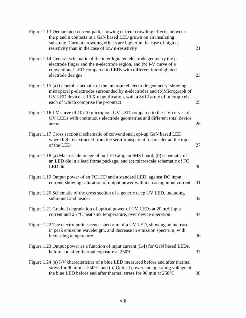
viii
Figure 1.13 Demarcated current path, showing current crowding effects, between
the p and n contacts in a GaN based LED grown on an insulating
substrate. Current crowding effects are higher in the case of high n-
resistivity than in the case of low n-resistivity 21
Figure 1.14 General schematic of the interdigitated electrode geometry the p-
electrode finger and the n-electrode region, and (b) I-V curve of a
conventional LED compared to LEDs with different interdigitated
electrode designs 23
Figure 1.15 (a) General schematic of the micropixel electrode geometry showing
micropixel p-electrodes surrounded by n-electrodes and (b)Micrograph of
UV LED device at 10 X magnification, with a 8x12 array of micropixels,
each of which comprise the p-contact 25
Figure 1.16 I-V curve of 10x10 micropixel UV LED compared to the I-V curves of
UV LEDs with continuous electrode geometries and different total device
areas 26
Figure 1.17 Cross sectional schematic of conventional, epi-up GaN based LED
where light is extracted from the semi-transparent p-spreader at the top
of the LED 27
Figure 1.18 (a) Macroscale image of an LED atop an IMS board, (b) schematic of
an LED die in a lead frame package, and (c) microscale schematic of FC
LED die 30
Figure 1.19 Output power of an FCLED and a standard LED, against DC input
current, showing saturation of output power with increasing input current 31
Figure 1.20 Schematic of the cross section of a generic deep UV LED, including
submount and header 32
Figure 1.21 Gradual degradation of optical power of UV LEDs at 20 mA input
current and 25 °C heat sink temperature, over device operation 34
Figure 1.22 The electroluminescence spectrum of a UV LED, showing an increase
in peak emission wavelength, and decrease in emission spectrum, with
increasing temperature 36
Figure 1.23 Output power as a function of input current (L-I) for GaN based LEDs,
before and after thermal exposure at 250°C 37
Figure 1.24 (a) I-V characteristics of a blue LED measured before and after thermal
stress for 90 min at 250°C and (b) Optical power and operating voltage of
the blue LED before and after thermal stress for 90 min at 250°C 38

ix
Figure 1.25 (a) 2-D SEM micrograph showing detachment of Ohmic contact layer
and (b) 3-D reconstruction of the same region 39
Figure 2.1 (a) Schematic of the cross section of a high power LFP an LED, (b) LFP
of a white light LED, and (c) picture of LFP showing thermal resistance
network 44
Figure 2.2 (a) Technical drawing of the TO66, with inset of a picture of the TO66,
(b) Technical drawing of the TO3, with inset of a picture of the TO3
package and (c) UV LED on TO3 package with visible wire bonds (a
TO66 package is also visible) 46
Figure 2.3 (a) Far field EL spectrum of a fresh UV LED, and (b) far field EL
spectrum of an aged UV LED showing a larger secondary emission peak 52
Figure 2.4 (a) Near field EL micrograph of a fresh UV LED emitting at 270 nm,
and (b) near field EL micrograph of an aged LED emitting at 270 nm 53
Figure 2.5 Plot of junction temperature measured by the Forward Voltage, Emission
Pea Shift and High Energy Slop Methods, against DC input current, for a
UV LED 55
Figure 2.6 Schematic of the Stokes Raman process, showing the incident photon
and the two stage transition that leads to the emitted Raman photon 56
Figure 2.7 The Stokes, anti-Stokes and Rayleigh peaks, showing peak
characteristics such as linewidth and peak position 57
Figure 2.8 (a) Effect of stress on the Raman peak position, and (b) general behavior
of the Raman peak with increasing temperature 58
Figure 2.9 Raman Stokes peak of Si, showing a decrease in wavenumber and
widening of the FWHM at a higher temperature 60
Figure 2.10 E2 high mode of n-Al0.2Ga0.8N at 574.2 cm-1
, used in the micro-Raman
thermometry of a UV LED by Sarua et al. 63
Figure 2.11 A temperature contour map over the surface area of the UV LED at a
c.w. input power of 400 mW, measured through Raman thermometry 65
Figure 2.12 Micro-Raman spectra of the UV LED at different input currents
investigated by Wang et al. 66
Figure 2.13 Setup of a CCD based thermoreflectance microscope 67
Figure 2.14 (a) The cumulative structure function of a green LED at a DC input
current of 400 mA, and (b) the differential structure function of the green
LED at a DC input current of 400 mA 70
x
Figure 3.1 Cross-sectional schematic of a micropixel device, showing the
multilayered composite device structure 75
Figure 3.2 Micrograph showing the electrode architecture of the micropixel device,
pointing to the p-contact and n-electrode regions 76
Figure 3.3 Micrograph of 4x4 array of 10x10 micropixel LEDs comprising the
Deep UV Lamp, under 5X magnification 77
Figure 3.4 Micropixel devices mounted on (a) a TO66 header and (b) a TO3 header.
The device mounted on the TO3 header is the DUVL 78
Figure 3.5 The four locations of micro-Raman measurements in the micropixel
device, shown in relation to the various layers in the device 79
Figure 3.6 Cross-sectional schematic of an interdigitated device, showing the
multilayered composite device structure 81
Figure 3.7 Micrograph showing the interdigitated electrode geometry of the
interdigitated device, depicting the p-mesa and the n-electrode 81
Figure 3.8 The lead-frame package of the interdigitated device 82
Figure 3.9 Locations of micro-Raman measurements in the interdigitated device,
shown in relation to the various layers in the device 83
Figure 3.10 IR thermograph of the interdigitated device, showing the region of
highest temperature in the device to be at the edge of p-mesa which was
also the location of micro-Raman measurements 83
Figure 3.11 (a) Setup of the Renishaw InVia Raman microscope system, and (b)
UV LED mounted on thermal stage, under the Raman microscope 85
Figure 3.12 (a) UV LED device with a TO66 package atop a 50mm x 60mm x
3.18mm copper mount, and (b) UV LED device with a lead frame
package atop a 50mm x 60mm x 3.18mm copper mount with a holder to
hold the curved surface of the package in place 87
Figure 3.13 QFI Infrascope II IR microscope, showing the location of the UV LED
on temperature controlled stage 90
Figure 3.14 Experimental setup of the EL spectroscopy method, showing optical
signal transmission to the spectrometer. The collimating lens is placed in
front of the operational LED in order to characterize EL output 92
Figure 3.15 Schematic showing setup of Forward Voltage temperature
measurements 94

xi
Figure 3.16 Forward voltage and junction temperature calibration curve for an LED
at pulsed at input currents between 20 mA to 100 mA, and for junction
temperatures between 35°C to 65°C 95
Figure 4.1 Raman spectrum between 514 cm-1
and 775 cm-1
of an unpowered
micropixel device at a thermal stage temperature of 25°C, showing the
Raman peaks of interest 99
Figure 4.2 Stokes peak shift calibration curve for the E2
high mode of AlN, showing
the peak shift coefficient, for a micropixel device 100
Figure 4.3 IV curve of the DUVL during reverse bias between voltages of -10.2 V
and 0 V 102
Figure 4.4 The temperature rises with increasing input powers in the sapphire layer
(Location III), the AlN layer (Location II) and the n- AlxGa1-xN layer
(Location I) over the p-mesa, in the DUVL, measured using micro-
Raman spectroscopy 103
Figure 4.5 Raman temperature rises with increasing input power, for the n- AlxGa1-
xN layer at the p-mesa (Location I), and the n-electrode (Location IV) in
the DUVL. The temperature rises at Location I have been corrected for
the effect of the inverse piezoelectric stress 106
Figure 4.6 (a) Micrograph of the DUVL device at a magnification of 1X, showing
the LED array where the micropixel with the hotspot was located, and (b)
IR thermograph of the micropixel with a hotspot, at a magnification of
5X 10⁸
Figure 4.7 Temperature rises in the AlN layer and the sapphire layer, measured by
Micro-Raman thermography, and the temperature rise measured by IR
thermography, with increasing input powers, for Device 1 112
Figure 4.8 Temperature rises in the AlN layer and the sapphire layer, measured by
Micro-Raman thermography, and the temperature rise measured by IR
thermography, with increasing input powers, for Device 2 113
Figure 4.9 Temperature rises in the AlN and sapphire layers, measured by Micro-
Raman spectroscopy, and temperature rise measured by IR
thermography, for Device 3 114
Figure 4.10 IR thermograph of Device 4 at a magnification of 5X showing
horizontal temperature differences on the surface of the device 116
Figure 4.11 Micro-Raman temperature rises in the AlN and sapphire layers,
measured for increasing input powers, for the Device 4 117

xii
Figure 4.12 EL spectra from the DUVL at a stage temperature of 50°C, at selected
c.w. input powers between 149 mW to 1.82 W 118
Figure 4.13 Shift in emission peak wavelength plotted against the change in
junction temperature, for the DUVL device at an input current of 300 mA 119
Figure 4.14 Emission spectra of the DUVL device at an input current of 300 mA, at
stage temperatures of 60°C, 80°C, 100°C 120
Figure 4.15 Calibration curve for the Vf method for Device 2 at input currents
between 10 mA and 25 mA 123
Figure 4.16 Calibration curve for the Vf method for Device 3 at input currents
between 10 mA and 25 mA 124
Figure 4.17 Junction temperature rise with increasing input power for micropixel
devices, measured using the Vf method 126
Figure 4.18 Raman spectrum between 566 cm-1
and 672 cm-1
, of an unpowered
interdigitated device, at a thermal stage temperature of 40°C 128
Figure 4.19 Temperature rises for various input powers, for the interdigitated
device, in the p-GaN and AlN layers measured through micro-Raman
spectroscopy, and from IR spectroscopy and the Forward Voltage
Method. The inset shows the cross sectional schematic of the
interdigitated device pointing to measurement locations 130
Figure 4.20 Forward Voltage method calibration curve for Device 5, an
interdigitated device, for input currents between 10 mA and 100 mA 133
Figure 4.21 Calibration curve for the Vf method for Device 6, an interdigitated
device, for input currents between 10 mA and 100 mA 134
Figure 4.22 Temperature rise with increasing input power for two interdigitated
devices, Devices 5 and 6, measured by the Vf method 135
Figure 5.1 Schematic of rectangular solid with heat flux boundary condition at the
plane x=0, z=0 140
Figure 5.2 Schematic of multilayered solid with heat flux boundary condition on
Layer 1, at the plane x=0, z=0 141
Figure 5.3 The Foster electrical circuit, showing node to node capacitances 143
Figure 5.4 The Cauer electrical circuit, showing node to ground capacitances 143
Figure 5.5 Schematic of experimental setup for the modified TRAIT method 146

xiii
Figure 5.6 (a) White light LED with IMS thermal substrate (b) Yellow light LED
(c) SMT white light LED (d) Deep UV LED on lead frame package 148
Figure 5.7 Schematic of cross-section of ANSYS model used to produce the
temperature transient of the junction of a packaged LED using ANSYS
based finite element analysis 150
Figure 5.8 Discretization of the ANSYS generated thermal transient of the LED
junction based on the change of slope of the time rate of change of the
thermal impedance of the device junction 151
Figure 5.9 The five stage Cauer circuit representation of the heat pathway out of the
junction of the LED, for the ANSYS generated thermal model of the
packaged LED 153
Figure 5.10 Temperature rise with time, for the ANSYS generated finite element
thermal model, and the results of the modified TRAIT method, at an
input power of 1W 154
Figure 5.11 Identification of thermal contributions, based on the time rate of change
of the thermal impedance of the junction of the white light LED with
thermal substrate 156
Figure 5.12 The two stage Cauer circuit representation of the heat pathway out of
the junction of the LED, for the white light LED with an IMS thermal
substrate 157
Figure 5.13 Temperature rise with time, for the white light LED with an IMS
substrate, from the experiment and the modified TRAIT method, at an
input power of 2.02 W 158
Figure 5.14 Identification of thermal contributions, based on the time rate of change
of the thermal impedance of the junction of the white light LED with
SMT power substrate 160
Figure 5.15 The two stage Cauer circuit representation of the heat pathway out of
the junction of the LED, for the white light LED with SMT power
substrate 160
Figure 5.16 Temperature rise with time, for the SMT white light LED, from the
experiment and the modified TRAIT method, at an input power of 0.888
W 162
Figure 5.17 Identification of thermal contributions, based on the time rate of change
of the thermal impedance of the junction of the yellow light LED 163
Figure 5.18 The two stage Cauer circuit representation of the heat pathway out of
the junction of the LED, for the yellow light LED 164

xiv
Figure 5.19 Temperature rise with time, for the yellow LED, from the experiment
and the modified TRAIT method, at an input power of 0.983 W 165
xv
SUMMARY
AlxGa1-xN (x>0.6) based Ultraviolet Light Emitting Diodes (UV LEDs) emit in the UV C
range of 200 – 290 nm and suffer from low external quantum efficiencies (EQEs) of less than
3%. This low EQE is representative of a large number of non-radiative recombination events in
the multiple quantum well (MQW) layers, which leads to high device temperatures due to self-
heating at the device junction. Knowledge of the device temperature is essential to implement
and evaluate appropriate thermal management techniques, in order to mitigate optical
degradation and lifetime reduction due to thermal overstress. The micro-scale nature of these
devices and the potential of temperature differences in the multilayered device structure merit the
use of several measurement techniques to resolve device temperatures.
This work investigates UV LEDs with AlxGa1-xN active layers, grown on sapphire or AlN
growth substrates, and flip-chip mounted onto submounts and package configurations with
different thermal properties. Thermal metrology results are presented for devices with different
electrode geometries (i.e., interdigitated and micropixel), for bulk and thinned growth substrates.
This work presents a comparative study of optical techniques such as Infrared (IR), micro-
Raman and Electroluminescence (EL) spectroscopy for the thermal metrology of internal device
temperatures in UV LEDs. The Forward Voltage (Vf) method, an electrical junction temperature
measurement technique, was also investigated. For the first time, Raman spectroscopy was used
to measure the temperature of discrete layers in an LED and comparisons made to other
techniques provided insight into the layer within the device they are sensitive to. Moreover, such
optical methods give further insight into the junction temperature of an operating LED which is
critical for developing device thermal models.

xvi
The forward voltage method was utilized to measure the packaging resistance of UV LEDs. A
new technique called Thermal Resistance Analysis by Induced Transient (TRAIT) procedure
was developed, whereby electrical data at short time scales from an operational device were used
to discretize the external junction-to- package thermal resistance of LEDs. The modified TRAIT
procedure was conducted on visible light LEDs, and yielded overall packaging resistance results
that agreed with published data and/or numerical modeling. The use of the TRAIT method
signifies a simple electrical resistance measurement technique that can yield insight into the
packaging thermal resistance of LEDs.
1
CHAPTER 1
INTRODUCTION AND MOTIVATION
1.1 Introduction to UV LEDs
Light Emitting Diodes (LEDs) are solid state devices that spontaneously emit light due to
the phenomena of electroluminescence in semiconductor materials. The optical emission from
LEDs depends on the choice of semiconductor materials that comprises the active region. The
first LED usable for commercial lighting purposes was demonstrated by Nick Holonyak Jr. in
1962, when coherent red light emission from a GaAsP device was seen [1]. Over the 1960s and
1970s, numerous developments were made in the materials growth and processing arena, which
allowed the introduction of LEDs for commercial illumination applications such as numeric
displays, by the start of the 1980s. Today, LEDs are widely used in numerous applications
ranging from signage to optical communications, and can emit across a wide range of the
electromagnetic spectrum.
Fig. 1.1 shows the wavelength and frequencies corresponding to different regions of the
electromagnetic spectrum, along with the wavelength scale, atmospheric penetrability and
equivalent blackbody temperature at highest intensity of emission. Currently, commercially
available LEDs emit between the Ultraviolet (UV) A and Infrared (IR) wavelengths between 365
nm and 1500 nm, encompassing the entire visible range [2, 3]. Visible light LEDs are now
widely used in traffic lights, signage systems, automotive ad aviation lights, backlighting for
electronic displays and household and commercial lighting [4]. IR LEDs are primarily used in
free space communications (such as in remote controls or between peripheral devices) and fiber
communications (such as through fiber –optic cables) [5]. UV LEDs emitting at wavelengths

2
longer than 360 nm are marketed commercially, and find use in chemical and biological agent
detection [6]. Recently, UV LEDs emitting as low as 210 nm have been shown, and UV LEDs
emitting between 210 nm and 365 nm are non-commercial LEDs still in stages of development
[7]. As LED technology for devices emitting in the visible and IR range is mature, scientific
focus is now shifting towards UV LEDs.
Figure 1.1. Properties of the electromagnetic spectrum across various frequencies and
wavelengths [8].
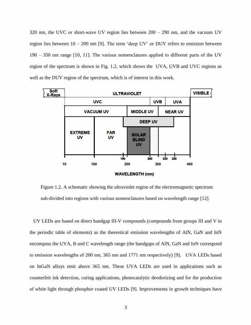
The UV region of the electromagnetic spectrum, which is defined as the region between 10 nm
and 400 nm, can be categorized into four different wavelength ranges. The UVA or long-wave
UV region lies between 320 nm and 400 nm, the UVB or mid-wave region lies between 290 to
3
320 nm, the UVC or short-wave UV region lies between 200 – 290 nm, and the vacuum UV
region lies between 10 – 200 nm [9]. The term ‘deep UV’ or DUV refers to emission between
190 – 350 nm range [10, 11]. The various nomenclatures applied to different parts of the UV
region of the spectrum is shown in Fig. 1.2, which shows the UVA, UVB and UVC regions as
well as the DUV region of the spectrum, which is of interest in this work.
Figure 1.2. A schematic showing the ultraviolet region of the electromagnetic spectrum
sub-divided into regions with various nomenclatures based on wavelength range [12].
UV LEDs are based on direct bandgap III-V compounds (compounds from groups III and V in
the periodic table of elements) as the theoretical emission wavelengths of AlN, GaN and InN
encompass the UVA, B and C wavelength range (the bandgaps of AlN, GaN and InN correspond
to emission wavelengths of 200 nm, 365 nm and 1771 nm respectively) [9]. UVA LEDs based
on InGaN alloys emit above 365 nm. These UVA LEDs are used in applications such as
counterfeit ink detection, curing applications, photocatalytic deodorizing and for the production
of white light through phosphor coated UV LEDs [9]. Improvements in growth techniques have

4
resulted in the production of large-chip InGaN UVA LEDs with an external quantum efficiency
(EQE) of 14.7 % which are able to emit 250 mW output power during continuous wave
operation at 500 mA. Smaller chip size LEDs with lower output powers are also marketed
commercially [9]. Further discussion about high bandgap materials, power conversion
efficiencies and dislocations will be provided in section 1.3, which will cover some of the
fundamental challenges to DUV LED development.
UVB and UVC LEDs are based on AlGaN and emit at wavelengths less than 320 nm,
encompassing the DUV region. DUV LEDs find applications in medical phototherapy and
widespread potential applications in air and water disinfection, biological agent sensing and solar
blind communications. DUV LEDs emitting between 280 and 320 nm find uses in
dermatological treatments using irradiation, such as for the disease psoriasis. DUV LEDs
emitting at the wavelengths of 269 nm and 282 nm have been found to inactivate Bacillus
subtilis spores in water flow [11]. And, light in the DUV wavelength ranges of 255 nm and 280
nm has also been shown to effectively deactivate strains of Escherichia coli and Enterococcus
faecalis [12]. DUV LEDs have also been shown to function as detectors for biological species
such as Bacillus globigii spores, airborne cellulose interferents such as cotton, paper and office
dust, as well as hydrocarbon particles such as diesel fuel. In such applications, the fluorescence
decay signature (i.e., the fluorescence spectra and lifetime) of the material to excitation from a
modulated near DUV LED optical signal was used to indicate the nature of the material to be
sensed, with the ability to discriminate between common interferents and bioparticles based on
the wavelength of excitation [13].
The use of DUV LED sources for disinfection and bioagent detection purposes is especially
advantageous compared to other UV light sources, such as easy disposability (since LEDs do not

5
contain scheduled substances such as mercury), compact design and increased physical durability
(because of the absence of glass bulbs), very short turn-on times and the ability to modulate
optically at high frequencies [11]. DUV LEDs emitting in the solar blind region of 200 nm- 280
nm also find potential applications in covert, short and medium range, non-line-of-sight (NLOS)
communications, owing to zero atmospheric background conditions and strong scattering
interactions within the solar blind region. The potential for applications of DUV LEDs in this
regard is compounded by the prospective of compact communication modules and low power
operations [14].
Various potential applications for DUV LEDs are shown in Figs. 1.3 and 1.4. Fig. 1.3 (a)
shows a test module with a flow chamber for the water disinfection application of the UV LED,
while Fig. 1.3 (b) shows the UV LED array and stirrer in the disinfection module. Fig. 1.4 (a)
details the scenarios in which NLOS DUV LEDs can be used as communication links, whereas
Fig. 1.4 (b) shows the transmitter and receiver of a first generation DUV LED communication
link.
(a) (b)
Figure 1.3. (a) DUV LED water disinfection unit showing flow chamber Würtele, et al. [11], and
(b) DUV LED array with stirrer rod, inside flow chamber [11].

6
(a)
(b)
Figure 1.4. (a) Different applications of DUV LEDs in NLOS systems and their attributes and
functions [15], and (b) first generation DUV LED communication link showing transmitter with
LED array, and receiver [15].
The low EQEs of DUV LEDs are a barrier to commercialization for these devices. Fig. 1.5
compares the EQE of UV LEDs emitting in the 200 nm to 400 nm range, identifying the research
group or organization that developed the UV LED. It can be clearly seen from Fig. 1.5 that in
general, the EQE of a UV LED decreases with a decrease in wavelength, with a UV LEDs
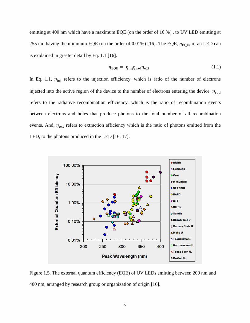
7
emitting at 400 nm which have a maximum EQE (on the order of 10 %) , to UV LED emitting at
255 nm having the minimum EQE (on the order of 0.01%) [16]. The EQE, , of an LED can
is explained in greater detail by Eq. 1.1 [16].
(1.1)
In Eq. 1.1, refers to the injection efficiency, which is ratio of the number of electrons
injected into the active region of the device to the number of electrons entering the device.
refers to the radiative recombination efficiency, which is the ratio of recombination events
between electrons and holes that produce photons to the total number of all recombination
events. And, refers to extraction efficiency which is the ratio of photons emitted from the
LED, to the photons produced in the LED [16, 17].
Figure 1.5. The external quantum efficiency (EQE) of UV LEDs emitting between 200 nm and
400 nm, arranged by research group or organization of origin [16].

8
The low EQE of a UV LED can be mainly be attributed reduced radiative recombination
efficiencies due to high defect densities in AlGaN [16]. Under continuous wave bias, UV LEDs
suffer from device self-heating, in part due to low radiative recombination efficiencies that result
in high rates of phonon emission. Device self-heating and high device temperatures significantly
reduce device time, and change device spectral emission [9]. The effect of high temperature on
UV LEDs will be discussed further in section 1.5.
1.2 Operating principles of an LED
An LED operates due to the spontaneous emission of photons when a forward bias is
applied across its junction. A junction is formed when two same (i.e., homojunction) or different
(i.e., heterojunction) semiconductor materials of opposite (anisotype) doping type are brought
together. In the case of an LED, p-type (i.e., acceptor doped) and n-type (i.e., donor doped)
semiconductor materials are brought together. Near the p-n junction, electrons from the n-doped
regions diffuse to the p-type region to recombine with holes. Conversely, holes from the p-doped
regions diffuse into the n-type regions to recombine with electrons. This creates a region in the
vicinity of the p-n junction known as the depletion region because of the reduced number of free
carriers in this region. The depletion region contains charges from ionized donors and acceptors,
which give rise to an electric potential called the diffusion voltage, or VD. The VD is the
minimum potential that free carriers must overcome in order to reach the oppositely doped
semiconductor. In highly doped semiconductors regions, as is found in LEDs, the VD is
approximately equal to the bandgap energy (Eg) divided by the elementary charge (e), VD = Eg/e.
When a forward bias greater than VD is placed on the diode, electrons from the n-doped region
are able to travel across the depletion region to recombine with holes, and vice-versa. Thus,

9
under forward bias, the current flow across the junction increases and the width of the depletion
region decreases [18] .
This is shown in Fig. 1.6 (a) and (b). Fig. 1.6 (a) shows the p-n junction under zero bias. Here,
EC is the conduction band edge, EV is the valance band edge, EF is the Fermi level and WD is the
width of the depletion zone. Fig. 1.6 (b) shows the p-n junction under a forward bias of V. In Fig.
1.6 (b), EFn and EFp are the quasi-Fermi levels at the n-type and p-type regions respectively.
Figure 1.6. (a) p-n junction of under zero-bias, and (b) p-n junction under a forward bias V,
showing narrowing of depletion region [19].
10
Under these conditions, electrons in the conduction band that undergo radiative recombination
with holes in the valance band produce a photon (only possible in direct band gap
semiconductors) with energy hν = Eg (where h is the Planck’s constant, and ν is the photon
frequency), or in an indirect transition to produce a photon and a phonon where the photon
energy is less than the bandgap of the junction [2]. LEDs contain quantum wells (QWs), which
are p-n junctions that consist of an active region (i.e., a semiconductor with a small bandgap)
surrounded by two barriers (i.e., semiconductors with a large bandgap). An electron injected in to
the junction is confined to the active region by the barriers, resulting in higher carrier
concentrations and increased radiative recombination. QW regions suffer from high resistance at
bandgap discontinuities, resulting in heating of the active region. In order to alleviate this
problem, band discontinuities of QWs are graded in chemical composition. Even with the
presence of barriers in a QW region, electron tunneling or carrier leakage from a well (the rate of
which increases at high current injection or high temperature) can result in carrier escape.
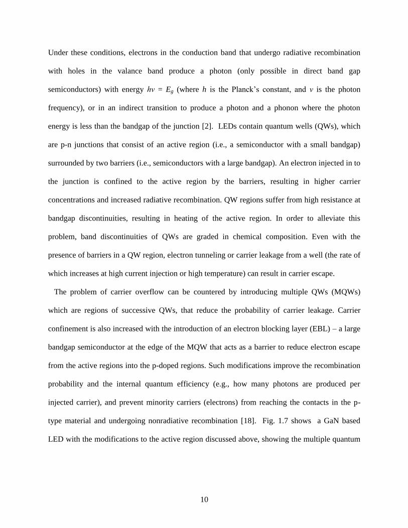
The problem of carrier overflow can be countered by introducing multiple QWs (MQWs)
which are regions of successive QWs, that reduce the probability of carrier leakage. Carrier
confinement is also increased with the introduction of an electron blocking layer (EBL) – a large
bandgap semiconductor at the edge of the MQW that acts as a barrier to reduce electron escape
from the active regions into the p-doped regions. Such modifications improve the recombination
probability and the internal quantum efficiency (e.g., how many photons are produced per
injected carrier), and prevent minority carriers (electrons) from reaching the contacts in the p-
type material and undergoing nonradiative recombination [18]. Fig. 1.7 shows a GaN based
LED with the modifications to the active region discussed above, showing the multiple quantum
11
wells to aid in radiative recombination, the electron blocking layer to prevent electron escape,
and the p- and n- doped confinement regions.
Figure 1.7. Schematic of active regions showing multiple quantum wells, the electron blocking
layers and the confinement regions in a GaN based LED [20].
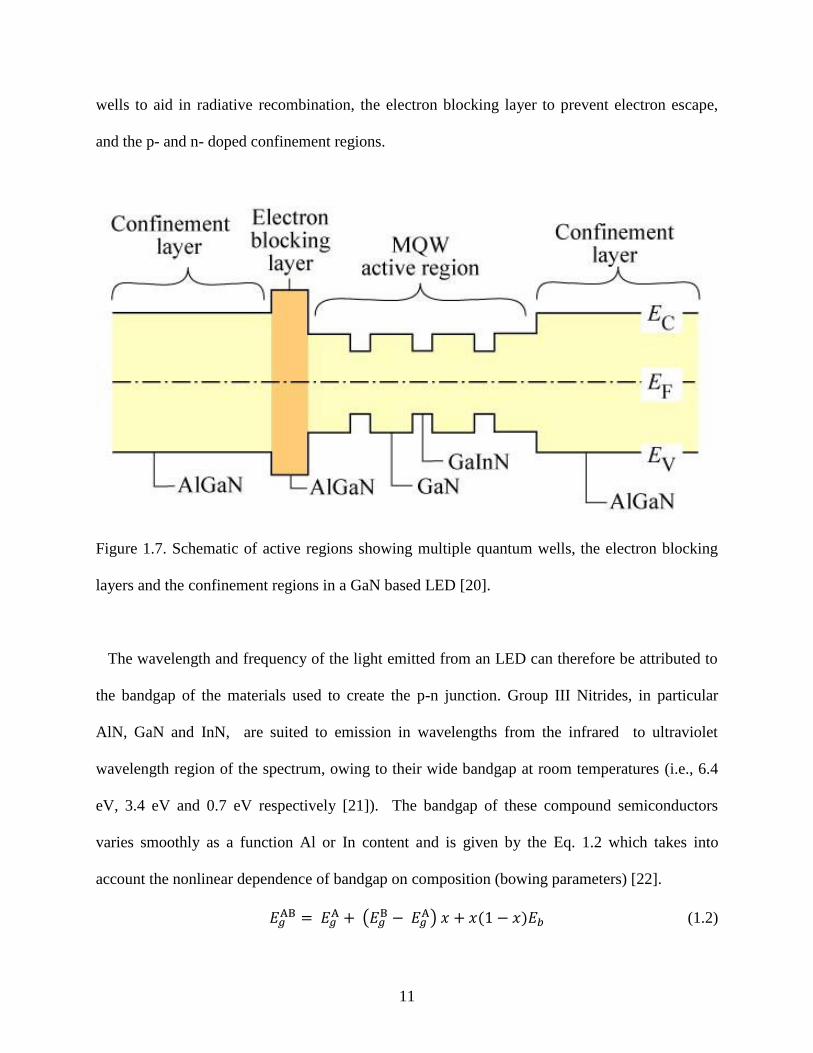
The wavelength and frequency of the light emitted from an LED can therefore be attributed to
the bandgap of the materials used to create the p-n junction. Group III Nitrides, in particular
AlN, GaN and InN, are suited to emission in wavelengths from the infrared to ultraviolet
wavelength region of the spectrum, owing to their wide bandgap at room temperatures (i.e., 6.4
eV, 3.4 eV and 0.7 eV respectively [21]). The bandgap of these compound semiconductors
varies smoothly as a function Al or In content and is given by the Eq. 1.2 which takes into
account the nonlinear dependence of bandgap on composition (bowing parameters) [22].
(
) (1.2)

12
In Eq. 1.2, is the bandgap of the compound semiconductor AB,
and are the bandgaps
of semiconductors A and B, is a constant linear term, and is the bowing parameter [22].
Additionally, the relationship between Eg in eV and emission wavelength λ in µm is given by Eq.
1.3.
(1.3)
From Eqs. 1.2 and 1.3, optical emission wavelength can be calculated for various III-V
compounds. For example, it can be found that for 0≤ x ≤ 1, InxAl1-xN can emit between 200 nm
and 1771 nm, InxGa1-xN can emit between 357 nm and 1771 nm, and AlxGa1-xN can emit
between 200 nm to 357 nm. The variation of Eg with lattice constant, a0, is shown in Fig. 1.8 for
InN, GaN and AlN. Fig. 1.8 also shows the colors of the visible spectrum that correspond to the
bandgap of ternary alloys of GaN and InN. Due to the unique property of changing
optoelectronic properties with mole fraction, it is possible to create the device structure shown in
Fig. 1.7 simply by changing the composition of the layers during the growth of the LED.
13
Figure 1.8. Plot of bandgap energy against lattice constants, for InN, GaN and AlN at room
temperature [22].
1.3 Fundamental challenges in the development of DUV LEDs
1.3.1 Challenge 1: Heteroepitaxial growth of high mole fraction AlxGa1-xN
One of the fundamental challenges with growing the high mole fraction (x≥0.5) AlxGa1-
xN required for DUV LEDs is the lack of optically transparent as well as lattice matched growth

14
substrates. AlN and GaN have a hexagonal wurtzite crystal structure, shown in Fig. 1.9. Fig 1.9
shows the AlxGa1-xN wurtzite crystal in the c-plane orientation (001). The lattice constants of
AlN and GaN, which are 3.112Å and 3.189Å, are also shown [23]. Due to the reasons of optical
transparency and the lack of more suitable substrates such as bulk AlN, AlxGa1-xN is usually
grown on sapphire, which has a lattice constant of 4.758 Å but displays a lattice mismatch of
16% with GaN and 12% with AlN due to its corundrum crystal structure [24].
Figure 1.9. Hexagonal wurtzite structure of AlN and GaN, showing crystal orientation and lattice
parameters [23].
High quality AlGaN, which is hard to grow due to the tendency of low surface mobility Al
adatoms to from a high density of dislocations and grain boundaries during the growth process.

15
Dislocations occur at or near the interface between two semiconductor materials having different
lattice constants, when they are grown on top of each other. Dislocations are characterized by
defects that occur as a result of dangling bonds at the interface between the two materials, also
called misfit dislocation lines, as shown in Fig. 1.10 [25].
Figure 1.10. Schematic of the interface between two semiconductors with a lattice mismatch,
showing the presence of dangling bonds [26].
Misfit dislocations may also start to form near the interface of two layers as well (as opposed to
at the interface) due to the fact that a thin semiconductor layer with the mismatched lattice
constant will initially be under elastic strain in order to assume the same lattice constant as the
underlying layer, but may relax to form defects [25]. When two layers with different lattice
parameters are able to conform to each other, the layer with the shorter lattice parameter under
tension the layer with the larger lattice parameter under compression, the resulting structure is
known is pseudomorphic. This is shown in Fig. 1.11 (a) and (b), which shows the thin layer of
16
semiconductor, with a lattice constant of a1, under elastic strain in order to conform to the
underlying lattice, with lattice constant a0.
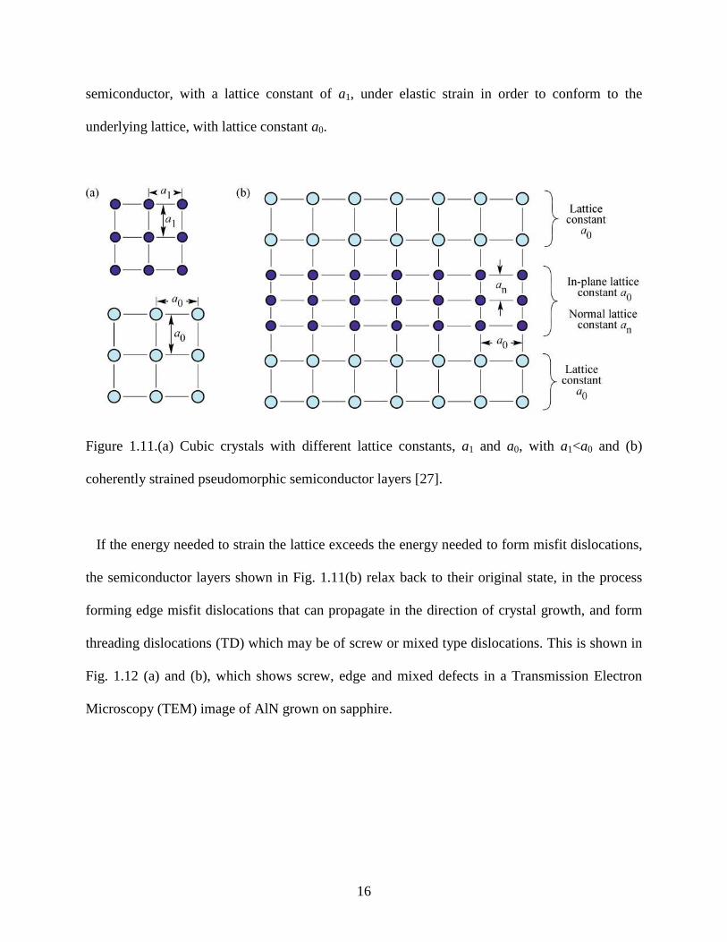
Figure 1.11.(a) Cubic crystals with different lattice constants, a1 and a0, with a1<a0 and (b)
coherently strained pseudomorphic semiconductor layers [27].
If the energy needed to strain the lattice exceeds the energy needed to form misfit dislocations,
the semiconductor layers shown in Fig. 1.11(b) relax back to their original state, in the process
forming edge misfit dislocations that can propagate in the direction of crystal growth, and form
threading dislocations (TD) which may be of screw or mixed type dislocations. This is shown in
Fig. 1.12 (a) and (b), which shows screw, edge and mixed defects in a Transmission Electron
Microscopy (TEM) image of AlN grown on sapphire.

17
Figure 1.12 (a) and (b). Screw, edge and mixed type dislocations seen in a TEM image of AlN
grown on sapphire through MOCVD, viewed under different directions [28].
The layer thickness (which is dependent on the lattice parameters and strain level) at which
misfit dislocations form is called the critical thickness, and can be calculated by the Matthew-

18
Blakeslee equation [29]. If the material layer is less than the critical thickness, thin defect free
layers can be grown even through the material layer may not be lattice matched to underlying
layers. Dislocations are positively or negative charged regions, which may act to repel or attract
the carrier depending upon its charge. In time, dislocations act as charge traps. For example, a
positively charged dislocation will attract electrons and repel holes. When enough electrons have
accumulated at the dislocation, columbic attraction between the holes and electrons will be
enough to overcome the dislocation potential, and the trapped electrons will then recombine non-
radiatively with holes to emit phonons. Thus, a high number of dislocations serve to reduce the
EQE of the LED device, and result in increased joule heating in the bulk semiconductor regions.
In III-V ternary alloy devices (such as DUV LEDs), the charge trapping effect of numerous
dislocations is overcome to some extent by compositional alloy fluctuations. These fluctuations
cause variations in the bandgap energy that serve to confine carriers before they reach the
dislocation regions, thus allowing for radiative recombination events to occur [30].
AlN and AlGaN alloys grown directly on sapphire using Metal-Organic Chemical Vapor
Deposition (MOCVD) method display threading dislocation densities in the range of 1010
to 1011
cm-1
, compared to 108 cm
-1 for GaN [28]. Additional degradation of the AlGaN layer happens
during the MOCVD growth process, wherein trimethylaluminum and triethylaluminum (used as
the metalorganic Al sources), react with ammonia (used as the N source),
cyclopentadienylmagnesium (used as the Mg source for p-doping) and silane (used as the Si
source for n-doping) to form adduct formations that reduce the quality of the AlGaN grown [9].
Pulsed Atomic-Layer Epitaxy (PALE) has been shown to be a solution to overcome the
challenges posed by MOCVD, demonstrating AlGaN with better surface morphology and
crystalline quality grown on AlN/sapphire template [31]. Pseudomorphic growth of thick AlGaN

19
on high quality bulk AlN has also been shown to be a solution to the MOCVD problem [32].
Approaches to grow high quality, high mole fraction AlGaN on AlN or AlN/sapphire also
include the addition of an Al rich strain layered superlattice to manage tensile strain and prevent
cracking in the AlGaN epitaxial layers [33].
Zhang et al. [34], developed the growth of low threading dislocation density (TDD) AlGaN
epilayers on AlN/AlGaN superlattices grown on sapphire substrates, using the Migration-
Enhanced MOCVD (MEMOCVD) method [34]. Hirayama et al., achieved the fabrication of
222-282 nm DUV LEDs based on AlGaN and InAlGaN active layers on low TDD AlN
templates grown on sapphire, where the AlN template were grown using the ammonia pulse-
flow multilayer (ML) technique [35]. Grandusky et al.[32] , developed a method to grow high Al
composition (0.45 to 0.75) pseudomorphic AlGaN layers up to 1.3µm thick on bulk AlN
substrates using MOCVD [32].
Despite these advances in growth processes, DUV LEDs suffer from low EQEs and output
power. This can be attributed to factors such as the Quantum Confined Stark Effect (QCSE),
absence of alloy clustering, low carrier confinement, optically absorbing templates and
substrates, the growth of AlGaN layers with low TDD and lateral current crowding [9]. These
factors will be discussed in more detail in Chapter 2. UV LEDs based on AlGaN and InAlGaN
active layers, emitting in the region of 280 nm to 350 nm have an EQE of 2% - 6% [16], while
UVC LEDs commonly have an EQE of around 1% , with the EQE decreasing as the emission
wavelength decreases. Recently, Pernot et al., exhibited an EQE of over 3% for AlGaN based
UV LEDs emitting between 255 nm to 280 nm [36].

20
1.3.2 Challenge 2: Current crowding in DUV LEDs
As UV LEDs are grown on electrically insulating substrates such as AlN or sapphire, the
p-electrode is located on top of the p-AlGaN mesa, and the n-electrode is located on top of the n-
AlGaN. As the Al composition in AlGaN is increased, n-and p-type doping of AlGaN becomes
much more difficult. This is due to the fact that the acceptors (p-dopants) in the AlGaN layer can
be passivated by the hydrogen used in the MOCVD growth. This leads to a highly resistive p-
AlGaN layer. The p-doping of AlGaN during the epitaxial growth process is also particularly
challenging due to the tendency of the Mg acceptors to diffuse into the active region, reducing
device recombination efficiency [33].
In order to provide an Ohmic contact to the resistive p-AlGaN, a thin layer of p-GaN is
deposited as a current spreading layer. However, this p-GaN serves to partially absorb UV
emission from the MQWs, decreasing the EQE of the LED. The nature of light extraction from
UV LEDs will be discussed in more detail in the Section 1.4. Additionally, the increased
resistivity of the Si-doped n-AlGaN with a high Al mole fraction in deep UV LEDs results in the
tendency for current to crowd on the edges of the p-mesa, between the n-electrode and the p-
electrode [33]. In LEDs with electrically insulating substrates, such as UV LEDs, the current
spreading length Ls (denoting the length from the electrode at which the current density drops to
1/e of the value of the current density at the edge of the electrode) is given by Eq. 1.4 below [37].
√( )
(1.4)
In Eq. 1.4, is the p-type specific contact resistance, and are the p-type cladding layer
electrical resistance and the thickness of the p-type cladding layer respectively, while and
are the n-type cladding layer and thickness of the n-type cladding layer. From Eq. 1.4, it is
apparent that for the effects of current crowding to be minimized, i.e. for to be maximized, the
21
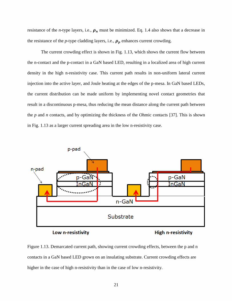
resistance of the n-type layers, i.e., must be minimized. Eq. 1.4 also shows that a decrease in
the resistance of the p-type cladding layers, i.e., enhances current crowding.
The current crowding effect is shown in Fig. 1.13, which shows the current flow between
the n-contact and the p-contact in a GaN based LED, resulting in a localized area of high current
density in the high n-resistivity case. This current path results in non-uniform lateral current
injection into the active layer, and Joule heating at the edges of the p-mesa. In GaN based LEDs,
the current distribution can be made uniform by implementing novel contact geometries that
result in a discontinuous p-mesa, thus reducing the mean distance along the current path between
the p and n contacts, and by optimizing the thickness of the Ohmic contacts [37]. This is shown
in Fig. 1.13 as a larger current spreading area in the low n-resistivity case.
Figure 1.13. Demarcated current path, showing current crowding effects, between the p and n
contacts in a GaN based LED grown on an insulating substrate. Current crowding effects are
higher in the case of high n-resistivity than in the case of low n-resistivity.

22
Electrode geometries to counter current crowding include micropixel and interdigitated electrode
geometries. In general, the micropixel electrode geometry consists of islands of p-electrodes,
with a diameter in the order of 10 µm, surrounded by n-electrodes. In contrast, the interdigitated
geometry consists of fingers of p-electrodes, interspersed by n-electrodes. The interdigitated
electrode design is shown in Fig. 1.14(a) and (b). Fig. 1.14 (a) shows a general schematic of the
interdigitated electrode geometry, showing the p-contact finger and the adjacent n-electrode. The
inset schematics in Fig. 1.14 (b) show two interdigitated design proposed by Kim et al. [38], as
well as the current-voltage (I-V) curve for the interdigitated design compared to a continuous
electrode design. It can be clearly seen from Fig. 1.14 that the devices with an interdigitated
electrode geometry exhibit superior electrical performance compared to the conventional
electrode geometry – requiring lower input currents for the same Vf [38].

23
(a)
(b)
Figure 1.14.(a) General schematic of the interdigitated electrode geometry the p-electrode finger
and the n-electrode region, and (b) I-V curve of a conventional LED compared to LEDs with
different interdigitated electrode designs [38].
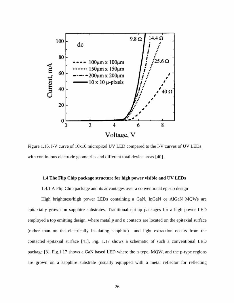
Adivarahan et al. [39] demonstrated a deep UV LED based on a micropixel electrode design
[40]. A general schematic of the micropixel is seen in Fig. 1.15 (a), showing the micropixels

24
surrounded by then –electrode. Fig. 1.15 (b) shows a micropixel array LED similar to the 10x10
micropixel array investigated by Adivarahan et al., where the diameter of each micropixel was
26 µm, and the total device area was approximately 500 µm x 500 µm. In Fig.1.15(b), the
micropixels form the p-contact whereas the space between the micropixels forms the n-contact.
The I-V curve of the micropixel UV LED compared to UV LEDs with continuous electrodes of
different total areas from Adivarahan et al. [40], is shown in Fig. 1.16. Fig. 1.16 shows that the
electrical performance of the 10x10 micropixel array UV LED is superior to that of the UV
LEDs with continuous electrode geometries, even though the continuous device electrodes had a
total device area considerably smaller than that of the 10x10 micropixel array (approximately
500 µm x 500 µm).

25
(a)
(b)
Figure 1.15. (a) General schematic of the micropixel electrode geometry showing micropixel p-
electrodes surrounded by n-electrodes and (b)Micrograph of UV LED device at 10 X
magnification, with a 8x12 array of micropixels, each of which comprise the p-contact .
26
Figure 1.16. I-V curve of 10x10 micropixel UV LED compared to the I-V curves of UV LEDs
with continuous electrode geometries and different total device areas [40].
1.4 The Flip Chip package structure for high power visible and UV LEDs
1.4.1 A Flip Chip package and its advantages over a conventional epi-up design
High brightness/high power LEDs containing a GaN, InGaN or AlGaN MQWs are
epitaxially grown on sapphire substrates. Traditional epi-up packages for a high power LED
employed a top emitting design, where metal p and n contacts are located on the epitaxial surface
(rather than on the electrically insulating sapphire) and light extraction occurs from the
contacted epitaxial surface [41]. Fig. 1.17 shows a schematic of such a conventional LED
package [3]. Fig.1.17 shows a GaN based LED where the n-type, MQW, and the p-type regions
are grown on a sapphire substrate (usually equipped with a metal reflector for reflecting

27
downward propagating modes of light). Light is extracted out of the top of the p-spreader, where
the Ni/Au current spreading layer, metal bond pads atop the Ni/Au layer, and wire bonds (wb)
are located. However, such top extracting LEDs exhibit lower EQEs because of light absorption
through the p and n contacts, bond pads and wire bonds in the package. The majority of optical
losses in an epi-up LED occur in the Ni/Au p Ohmic metallization layer, which is ideally thick
enough (>500 Å) to prevent current crowding, but is optimized in thickness to prevent light
absorption. The compromised p contact thickness leads to a lower WPE in a conventional LED
design [41].
Figure 1.17. Cross sectional schematic of conventional, epi-up GaN based LED where light is
extracted from the semi-transparent p-spreader at the top of the LED [3] .

28
Flip Chip (FC) LEDs employ a package design wherein the die is inverted such that light
extraction is conducted through the sapphire substrate. The FC LED structure consists of a
highly reflective p contact that redirects light propagating in the downward direction up through
the transparent substrate, and can be thick enough to ensure high current spreading and low
forward voltages, and thus a higher wall plug efficiency (or WPE, the ratio between power to
output optical power to input electrical power). The FC LED structure also prevents optical
absorption in the metal contacts and the wire bonds, and is able to extract downward propagating
modes of light, resulting in an increased EQE [41]. The FC structure also shows significant
thermal advantages compared to the conventional epi-up structure, as the thermal pathway out of
the LED junction is now through the p and n contact metallization, which is soldered to a
thermally conductive submount and power substrate [42].
Fig. 1.18 shows the multiscale breakdown of a commercial FC LED. The macroscale image of
the LED package in Fig. 1.18 (a) shows an LED on a lead frame package atop an Insulated Metal
Substrate (IMS) board. Fig. 1.18 (b) provides a more detailed view of the lead frame package,
showing the solder connection between the LED and the Si submount, and the gold wire bonds
to the metal contacts on the power substrate. The Si submount is then attached to a Cu heat sink.
In case of a white light LED, the assembly is enclosed with a plastic lens (usually a silicone
epoxy encapsulant). The frame also has anode and cathode leads that provide a connection to an
external electrical circuit. The microscale schematic of the LED die in Fig. 1.18 (c) shows light
extraction out of the sapphire substrate, including light reflected from the p contact, and the
solder bumps that provide a thermal and electrical connection between the p and n contacts on
the die and the power substrate metal contacts and submount below. Fig. 1.18 (c) also shows the
wire bonds from the anode and cathode leads bonded to the power substrate metal contact,

29
eliminating the need to wire bond to contact pads directly on the die, as seen in the schematic of
a conventional epi-up package in Fig. 1.17.
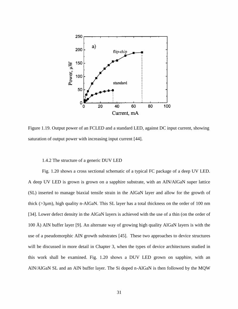
Flip chip LEDs have been known to provide better performance compared to conventional
LEDs, and have shown greater light output and lower levels of thermal derating (i.e., droop).
This is seen in Fig. 1.19, which compares the light output of an FC LED a standard LED, to DC
input current. Fig. 1.19 shows an increase in saturation current level (70 mA compared to 35
mA), and an increase in output power (by a factor of 3) for the FC LED as compared to a
standard LED.

30
Figure 1.18. (a) Macroscale image of an LED atop an IMS board, (b) schematic of an LED die in
a lead frame package, and (c) microscale schematic of FC LED die [43].
(a)
(b)
(c)
31
Figure 1.19. Output power of an FCLED and a standard LED, against DC input current, showing
saturation of output power with increasing input current [44].
1.4.2 The structure of a generic DUV LED
Fig. 1.20 shows a cross sectional schematic of a typical FC package of a deep UV LED.
A deep UV LED is grown is grown on a sapphire substrate, with an AlN/AlGaN super lattice
(SL) inserted to manage biaxial tensile strain in the AlGaN layer and allow for the growth of
thick (>3µm), high quality n-AlGaN. This SL layer has a total thickness on the order of 100 nm
[34]. Lower defect density in the AlGaN layers is achieved with the use of a thin (on the order of
100 Å) AlN buffer layer [9]. An alternate way of growing high quality AlGaN layers is with the
use of a pseudomorphic AlN growth substrates [45]. These two approaches to device structures
will be discussed in more detail in Chapter 3, when the types of device architectures studied in
this work shall be examined. Fig. 1.20 shows a DUV LED grown on sapphire, with an
AlN/AlGaN SL and an AlN buffer layer. The Si doped n-AlGaN is then followed by the MQW

32
regions, and the Mg doped p-AlGaN region and the p-contact region. The MQW region consists
of p and n doped confinement layers, designed to prevent electron and hole escape from the
quantum well region, and quantum wells between the confinement layers [9]. The p-AlGaN is
followed by a layer of high electrical conductivity p-GaN for current spreading into the p-
regions, and for ease of Ohmic contact formation compared to the electrically resistive p-AlGaN
material [9]. The p and n contacts are then gold bonded to contact pads on top of a thermally
conductive submount, shown in Fig. 1.20 as AlN. The submount is then bonded to a header that
can be mounted on a thermally dissipating heat sink, using high thermal conductivity solder.
Here on end, in this work, the use of the word UV LED will convey a DUV LED with the
general structure seen in Fig. 1.20.
Figure 1.20. Schematic of the cross section of a generic deep UV LED, including submount and
header [9].
33
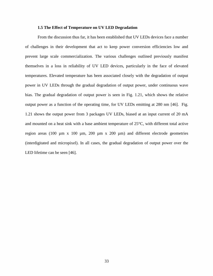
1.5 The Effect of Temperature on UV LED Degradation
From the discussion thus far, it has been established that UV LEDs devices face a number
of challenges in their development that act to keep power conversion efficiencies low and
prevent large scale commercialization. The various challenges outlined previously manifest
themselves in a loss in reliability of UV LED devices, particularly in the face of elevated
temperatures. Elevated temperature has been associated closely with the degradation of output
power in UV LEDs through the gradual degradation of output power, under continuous wave
bias. The gradual degradation of output power is seen in Fig. 1.21, which shows the relative
output power as a function of the operating time, for UV LEDs emitting at 280 nm [46]. Fig.
1.21 shows the output power from 3 packages UV LEDs, biased at an input current of 20 mA
and mounted on a heat sink with a base ambient temperature of 25°C, with different total active
region areas (100 µm x 100 µm, 200 µm x 200 µm) and different electrode geometries
(interdigitated and micropixel). In all cases, the gradual degradation of output power over the
LED lifetime can be seen [46].
34
Figure 1.21. Gradual degradation of optical power of UV LEDs at 20 mA input current and 25
°C heat sink temperature, over device operation [46].
Shatalov et al. [46], found that the gradual decay of output power took place with two
characteristic time constants; the faster time constant being bias current dependent and
temperature dependent, while the slower time constant decreased exponentially with a rise in
junction temperature. It was also found that for device and package configurations with large
thermal resistances in heat pathways out of the junction, the slower time constant dominated the
gradual degradation mechanism [46]. Thus, temperature has a significant influence on the
electrical and spectral characteristics of a UV LED.
1.5.1 The Coupling Between Elevated Temperature and Non-Radiative Recombination

35
Elevated device temperature has been shown to increase the peak emission wavelength
and decrease the emission intensity in AlGaN based UV LEDs. This is shown by Cao et al., in
Fig. 1.22, which shows the electroluminescence (EL) spectra of a UV LED (emitting at 280 nm
at 25°C) between 25°C and 175°C [47]. The spectral shift to high wavelength and lower
emission intensity can clearly be seen in Fig. 1. 22, when at 175°C the emission intensity of the
UV LED has been reduced by a factor of 48 of its original value. The decreased optical
efficiency of UV LEDs with an increase in temperature, at moderate and high input current
densities, is found to be coupled with an increase in non-radiative recombination at the junction
through two mechanisms. Firstly, at high temperatures, carries injected into the p-n junction have
a higher thermal energy and are more likely to escape, which increase the probability of non-
radiative recombination outside the junction. Secondly, the non-radiative recombination rate
inside the junction increases with an increase in device temperature, leading to a decrease in the
radiative recombination efficiency [47, 48] .

36
Figure 1.22. The electroluminescence spectrum of a UV LED, showing an increase in peak
emission wavelength, and decrease in emission spectrum, with increasing temperature [47].
1.5.2 Degradation of Ohmic Contacts and p-Type Regions at High Temperatures
High temperature stress has been known to cause degradation in GaN based LEDs, by
altering the electrical characteristics of the LED and causing the operating voltage of the LED to
increase and the optical power to decrease. This has been correlated with lowering the acceptor
concentration at the p-type regions, increasing the resistivity of the metal contacts at the
electrode and the p-type neutral regions, broadening of the Schottky barrier at the p-electrode
ohmic contact, and decreasing current distribution uniformity [48, 49]. The effect of thermal
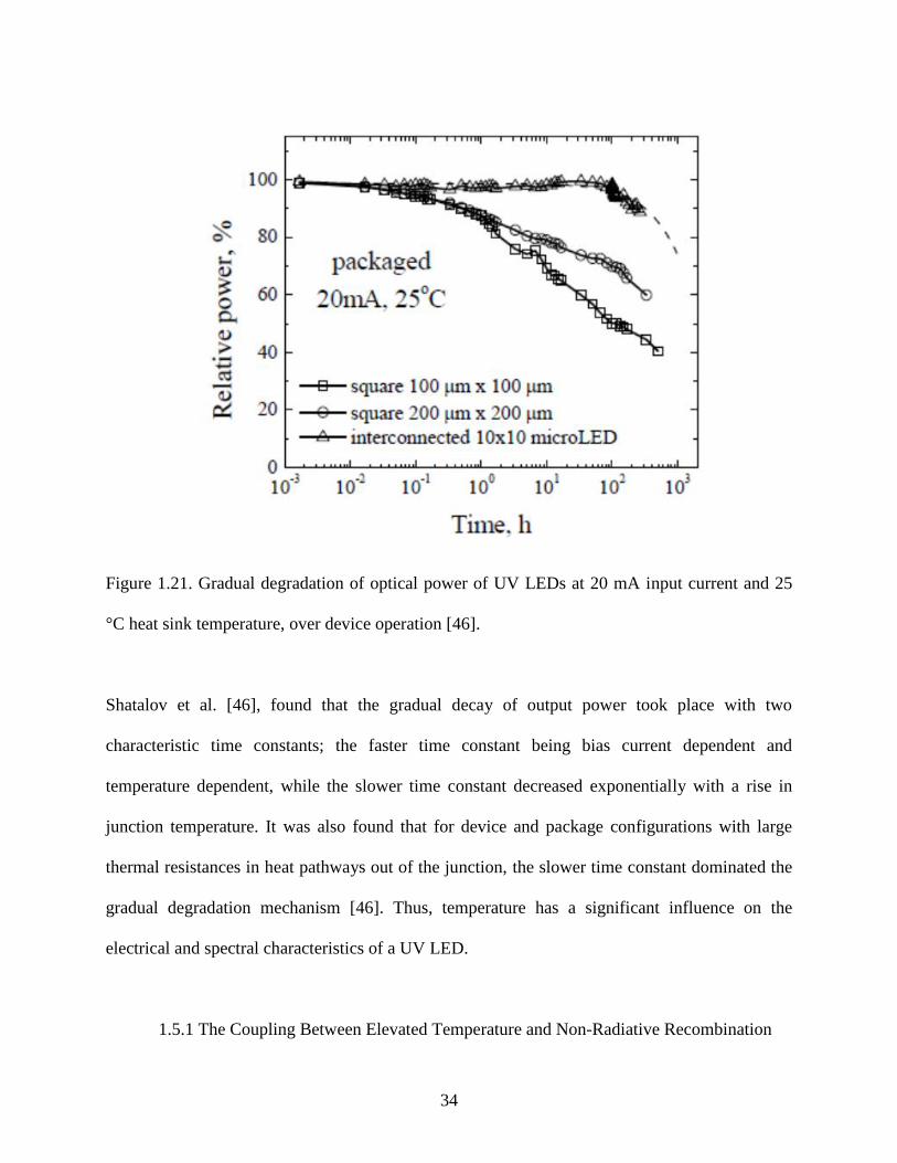
stress on the light output of a GaN based LED is seen clearly in Fig. 1.23, which shows the
output power of the LED at a continuous wave bias, before and after exposure to thermal stress
37
at 250°C. In particular, Fig. 1.23 shows that thermal exposure resulted in the degradation of
optical power by 47% at an input current of 20 mA, after thermal exposure for 160 hours [50].
Figure 1.23. Output power as a function of input current (L-I) for GaN based LEDs, before and
after thermal exposure at 250°C [49].
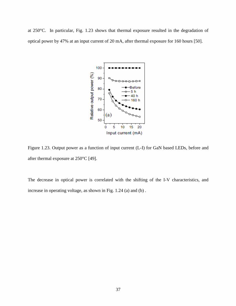
The decrease in optical power is correlated with the shifting of the I-V characteristics, and
increase in operating voltage, as shown in Fig. 1.24 (a) and (b) .
38
(a) (b)
Figure 1.24. (a) I-V characteristics of a blue LED measured before and after thermal stress for 90
min at 250°C [48] and (b) Optical power and operating voltage of the blue LED before and after
thermal stress for 90 min at 250°C [48].
High temperature and/or high current densities has also been reported to cause a partial
detachment of the contact metallization layers, due to poor adhesion between the layers at the
metal contact under high stress conditions, and the thermal mismatch between different materials
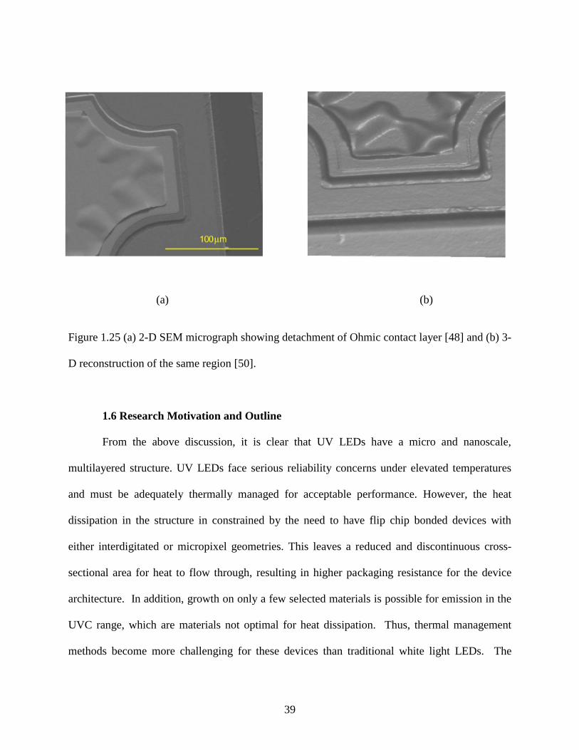
used in the contact layers [48]. Fig 1.25 (a) and (b) show the Scanning Electron Microscopy
(SEM) image of the detachment of the Ohmic contact layer due to thermal and/or current stress
[48, 50]. Thermal management techniques are therefore necessary to mitigate the effects of
thermal stress an elevated temperature on UV LED degradation.
39
(a) (b)
Figure 1.25 (a) 2-D SEM micrograph showing detachment of Ohmic contact layer [48] and (b) 3-
D reconstruction of the same region [50].
1.6 Research Motivation and Outline
From the above discussion, it is clear that UV LEDs have a micro and nanoscale,
multilayered structure. UV LEDs face serious reliability concerns under elevated temperatures
and must be adequately thermally managed for acceptable performance. However, the heat
dissipation in the structure in constrained by the need to have flip chip bonded devices with
either interdigitated or micropixel geometries. This leaves a reduced and discontinuous cross-
sectional area for heat to flow through, resulting in higher packaging resistance for the device
architecture. In addition, growth on only a few selected materials is possible for emission in the
UVC range, which are materials not optimal for heat dissipation. Thus, thermal management
methods become more challenging for these devices than traditional white light LEDs. The

40
evaluation and implementation of thermal management techniques requires the measurement of
device temperature. However, due to the complex internal structure of UV LEDs, it is not clear
if temperature differences exist in the device or the exact value of the junction temperature. As
of today, no thermal measurement techniques for LEDs even consider the possibility of thermal
differences and discontinuities in the device architecture.
To address the needs for thermal metrology in UV LEDs, we will investigate state of the art
measurement techniques for the temperature measurements such as the electrical response of the
LED (the Forward Voltage Method), the optical scattering of the semiconductor layers in the
device (micro-Raman and Infrared spectroscopy) or measure the parameters of optical emission
from the device (Electroluminescence spectroscopy). Through the use of Raman spectroscopy,
we propose to be the first to interrogate the temperature of specific layers in the device
architecture. The contribution of this work is particularly important because no studies have thus
far focused on thermal metrology of UV LEDs that relate the temperature distribution inside the
layers of the UV LED to its junction temperature, or present a way to find the package resistance
of the UV LED. This work describes the efforts taken to measure the temperature internal to the
UV LED, i.e., the temperature of the layers inside the UV LED and the LED junction, and to
measure the thermal resistance external to the LED, i.e., thermal resistance of the LED package.
An outline of chapters 2 through 6 in this work are given:
(a) Chapter 2 – Chapter 2 begins with a description of lead frame and TO packages,
which are the two types of packages common among UV LED manufacturers. A
literature review of some common thermal metrology techniques for high power
visible and UV LEDs is provided, along with a discussion of the thermal metrology
results from other groups and authors. Also presented in Chapter 2 are principles of

41
the thermal metrology techniques for measuring temperatures internal to the LED
(micro-Raman, Infrared (IR) and Electroluminescence (EL) spectroscopies, and the
Forward Voltage method). The background for these techniques is presented before
discussion of literature studies that utilize these techniques.
(b) Chapter 3 – Chapter 3 defines the two types of UV LEDs that are studied in this work
(micropixel and interdigitated LEDs). The locations of measurement inside the device
are specified. And, the instrumentation and experimental method for internal
temperature measurement techniques are outlined.
(c) Chapter 4 – Chapter 4 presents the experimental results for internal temperature
measurements for the micropixel and interdigitated devices. Comparisons will be
made between temperature distribution in internal device layers and junction
temperature measurements, and temperature measurements of a hotspot will be
presented. Some issues encountered with measuring junction temperature based on
electrical properties of the UV LED will also be discussed.
(d) Chapter 5 – Chapter 5 presents the principle, experimental method and experimental
results of the modified TRAIT method, for thermal resistance measurements external
to the LED. The junction to package thermal resistance is discretized for the total heat
pathway for devices of interest using the modified TRAIT method.
(e) Chapter 6 – Chapter 6 summarizes the main findings from this study and highlights
new contributions made to the field of UV LED thermal metrology through this work.
A summary discussion of the advantages and disadvantages of the various techniques
and opportunities for future work is discussed.

42
CHAPTER 2
UV LED PACKAGING AND LITERATURE REVIEW OF UV LED
THERMAL METROLOGY
This chapter begins with a review of the two types of packages of concern in this work, i.e., lead
frame package and the TO package, which are the common packages employed by the industry
for UV LEDs. The chapter continues on to a literature review of common thermal metrology
methods employed to measure device temperatures and package thermal resistances in UV
LEDs. Before discussion of literature studies foe internal device temperature measure
techniques, a discussion of the principles of the technique is provided.
2.1 Packaging schemes for high power LEDs
2.1.1 Lead Frame Package
The Lead Frame package (LFP) is the first type of package of relevance in this work, as it
is the type of packaging for interdigitated devices which have been investigated. The LFP
contains an LED that has been soldered to a reflective cup, aimed to increase optical intensity by
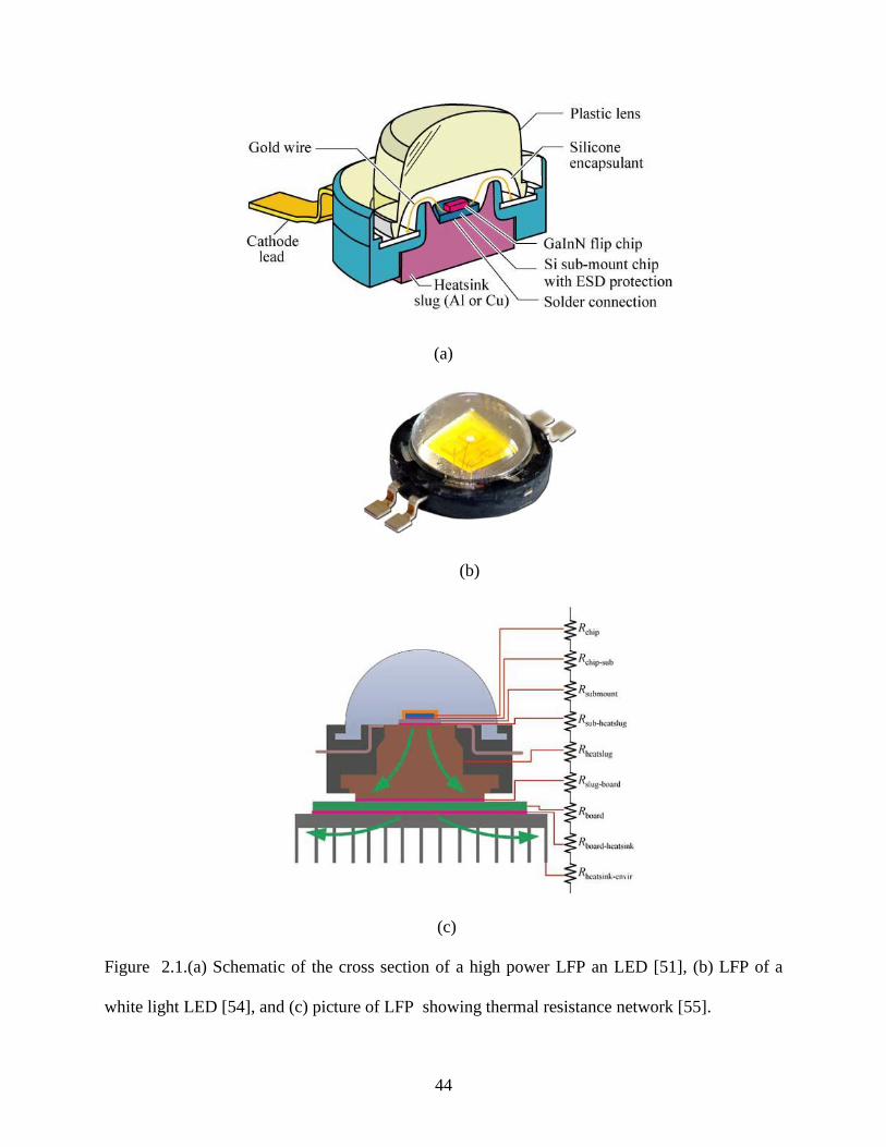
shaping the distribution of the emitted light. Fig. 2.1(a) shows the cross sectional schematic of an
LFP for a high power LED, pointing to the direct thermal path from the base of the LED die to
the surroundings through the high thermal conductivity Cu or Al heat slug. It must be noted that
the LFP package with a silicone lens and a plastic lens cover shown in Fig. 2.1(a) is applicable
only to visible LEDs. Fig. 2.1(a) also shows the LED with a thermally conductive submount (in
this case, Si) rated for protection against electrostatic discharge [51]. A detailed thermal analysis
of temperature rise in high power LFP packages can be found in Christensen et al. [52]. The LFP

43
is a surface mount (SMT) package, since it allows the device to be soldered on to a printed
circuit board (PCB). This results in flexibility of LED placement in applications, but decreases
LED density. Fig. 2.1(b) shows the LFP OF a white light LED, including the encapsulant lens.
The wire bonds between the electrical contact pads in the package and the bond pads of the epi-
up LED are visible. The electrical leads of LFP are also visible.
Fig. 2.1(c) shows the thermal resistance network corresponding to a LFP mounted onto a
circuit board atop a finned heat sink. The LFP allows for the spreading of heat from the LED die
through the high thermal conductivity slug, and shows a thermal resistance between 4-10 K/W
[53]. The LFP of the interdigitated devices uses in this investigation contained a Cu heat slug.
44
(a)
(b)
(c)
Figure 2.1.(a) Schematic of the cross section of a high power LFP an LED [51], (b) LFP of a
white light LED [54], and (c) picture of LFP showing thermal resistance network [55].

45
2.1.2 Transistor outline package
Transistor Outline packages (TO) are common packages used for semiconductor devices
correspond to physical dimensions set by the microelectronics industry governing body JEDEC
for packages for transistor chips. In this investigation, TO3 and TO66 package types for
micropixel LEDs are encounter. TO packages are made of two layers of high thermal and
electrical conductivity material, typically Cu or Au, enclosing a layer of BeO which acts as a
high thermal conductivity electrical insulator. A typical TO package will have protruding pins
that allow for electrical connectivity to an external circuit. TO packages allow for flexibility of
mounting to various configurations because of their standardized geometry, can handle large
power loads because of the heat dissipation capabilities of the large metal package, and can be
attached to an external heat sink with ease. Technical drawings of the TO66 and TO3 packages,
with relevant package dimensions are shown in Figs. 2.2(a) and 2.2(b) respectively. Fig. 2.2(a)
and (b) also contain the micropixel UV LEDs in this investigation on TO66 and TO3 packages in
the inset. Note that the thickness of the TO66 package is 1.9 mm, compared to the thickness of
the TO3 packages, which is 3.2 mm. In this case, the LED is attached to the surface of the TO
package and wirebonded to the leads on the TO structure. A cap can be placed over the LED to
protect it from the environment. For UV LEDs, it is critical that the lens on the cap be
transparent to the wavelength of radiation being emitted by the LED. Fig. 2.2(c) shows a UV
LEDs on a TO3 package. Wire bonds from posts, which are the external electrodes, to the
devices can be seen. A TO66 package is also visible behind the TO3 package in Fig. 2.2(c).

46
(a)
(b)
(c)
Figure 2.2.(a) Technical drawing of the TO66 [56], with inset of a picture of the TO66, (b)
Technical drawing of the TO3 [57], with inset of a picture of the TO3 package and (c) UV LED
on TO3 package with visible wire bonds (a TO66 package is also visible).

47
2.2 Metrology techniques for high power UV LEDs and literature review of key
studies
2.2.1 Principles of the Forward Voltage Method
(a) The relationship between forward voltage and junction temperature :
The Vf of a diode under a forward current (If) input is a temperature dependent quantity,
whose dependence on the Tj is given by Eq. 2.1 below [58]. In Eq. 1, Vf is the forward voltage
of the LED, Tj is the absolute temperature at the junction of LED, and A and B are the coefficient
and intercept of the linear relationship, respectively.
(2.1)
The coefficient A is negative, signifying a decrease in Vf with a unit increase in . It is also
known as the K-factor, or the temperature coefficient of voltage [59]. Eq. 2.1 is valid for a
particular If, as B changes for different levels of current input [58]. In cases where the diode
electrical properties are not invariant, A can also change for differing input currents. A and B are
unique to devices whose MQWs and bulk regions have particular electrical properties, and
therefore need to be determined for different LED makes and models. A and B can be found from
a calibration measurement, the technique for which is discussed in Chapter 3.
(b) The components of the Vf of an LED and the various factors that influence it
The Vf across a forward biased LED is the sum total of contributions from the diode
voltage (i.e., equal to the bandgap energy of the MQW divided by the elementary charge Eg/e),
the voltage drop due to non-adiabatic carrier injection into a single or double QW heterostructure
resulting in phonon emission, and the voltage drop sue to the series resistance in the diode

48
Ohmic contacts, in bulk semiconductor regions with low electron mobilities or high defect
densities, and across abrupt heterostructure interfaces [60] . The series resistance term also
includes the impact of current crowding between the p and n contacts. These contributions are
seen in the expression for the Vf in Eq. 2.2.
(2.2)
In Eq. 2.2, is the bandgap of the quantum well, e is the electron charge, is the forward
current, is the series resistance in the current path, is the band discontinuity of the
conduction band, is the band discontinuity of the valance band, and is the energy of the
lowest quantized state in the conduction or valance bands. The temperature dependence of Eg is
given by the Varshni formula, shown in Eq. 2.3.
(2.3)
In Eq. 2.3, is the bandgap of the semiconductor at 0K, T is the temperature of the
semiconductor materials, and and are the Varshni parameters [61]. From Eqs. 2.2 and 2.3, it
can be concluded that all other factors remaining equal, when the Tj increases, the Vf will
decrease due to the decrease in Eg. Thus, the measured Tj from Eq. 2.1 will accurately reflect the
increase in temperature, based on the effects of Eg on Vf. However, in reality, the contribution of
other terms in Eq. 2.2 on the Vf cannot be ignored.
The contribution of Ohmic contact degradation (in GaN based LEDs) on the Rs term in Eq. 2.2
increases at high current or high temperature stress, when the resistivity of the p-GaN layer and
the p-contact layer becomes higher due to diffusion chemical reactions and the formation of
electrically active defects caused by thermo-mechanical stress and deformation of the p-contact
[48, 62]. Note that Rs also contains contributions from the series resistance in the electrical
circuit external to the LED, and that variability in the external circuit must be account for when
49
using the Vf method. The contribution from the phonon emission terms in Eq. 2.3 also manifests
itself through different mechanisms at the low current density and the high current density
regimes. At low current injection levels, trapping of electrons and subsequent phonon emission
takes place due to defect generation in the active layers [63]. This leads to an increase in Vf, and
therefore a calculated decrease in Tj (all other factors being equal).
At high current injection regimes (or at high temperatures), carrier overflow from the active
region occurs, and carriers may combine non-radiatively in the barrier region or in the bulk p
regions [64]. Phonon emission at high current densities leads to an increase in Vf and an apparent
decrease in Tj. Thus, the Vf of an LED cannot be assumed to be a completely invariant measure
of Tj , and must be supplemented by other temperature or optical measurements as the LED ages,
so that the change in Vf due to the change in diode electrical properties can be clarified. The use
of the Vf method for temperature measurements on UV LEDs can particularly misleading, as the
electrical properties of the relatively less-mature UV LEDs are known to show variability with
degradation during device operation [48, 65]. In addition to UV LEDs, the Vf method to measure
junction temperature has been investigated in a number of studies involving light emitting and
other types of diodes.
(c) The temperature coefficient of voltage
The theoretical expression for the temperature dependence of Vf derives from Shockley’s
equation for the current density in an ideal p-n junction, given by Eq. 2.4.
( ⁄ ) (2.4)
In Eq. 2.4, J is the current density in the p-n junction, Js is the saturation current density at the
junction, e is the elementary charge, nideal is the diode ideality factor, k is the Boltzmann constant,

50
and T is temperature [61]. Under forward bias, the temperature dependency of the Vf is derived
from Eq. 2.4 and yields Eq. 2.5 below [61, 66] . The temperature coefficient of voltage in Eq. 2.5
contains contributions from the temperature dependences of the intrinsic carrier concentration,
bandgap energy, the effect density of states, and the series resistances, as shown by the first,
second, third and fourth summands respectively.
(
)
(2.5)
In Eq. 2.5, ND and NA are the donor and acceptor concentrations, respective. And, Nc and Nv are
the effective density of states at the conduction band edge and the valance band edge,
respectively. The temperature coefficient of voltage shows a weak dependence on temperature,
based on the contribution from the temperature dependence of bandgap (i.e., the second
summand). Thus, under ideal conditions, the temperature dependence of Vf, i.e., the coefficient A
in Eq. 2.1, should be a constant for a particular If. However, A might vary with LED aging
conditions, if the temperature sensitivity of the series resistance (i.e., the fourth summand) is
non-constant. In addition, from Eq. 2.2, the intercept B in Eq. 2.1 (which can be interpreted at the
Vf at 0 K) will also vary as the series resistance of the diode changes with device degradation. As
a consequence of the fact that A and B can be invariant, the factors affecting the validity of Vf
method calibration must be kept in mind when performing temperature measurements.
2.2.2 Electroluminescence spectroscopy
Electroluminescence (EL) is the phenomenon of light emission from an LED when
provided with an input power. The EL spectrum of an LED is capable of providing valuable
information about the junction temperature in the device, and can also give information about the
state of device degradation. EL spectra can be used for junction temperature measurement of the

51
LED using the peak emission shift method, or the high energy slope method. In the peak
emission shift method, the variation between Tj and the peak emission wavelength of the UV
LED is established through a pulsed input current calibration. When the UV LED is then
supplied with a c.w input current, the resulting output light spectra is been used to characterize
Tj, based on the knowledge of peak emission shift with increase in Tj from calibration
measurements [67].
The theoretical dependence of the peak emission wavelength with temperature is based upon
the Eg of the MQW region, due to the fact that Eg is temperature sensitive, in keeping with the
Varshi formula shown in Eq. 2.3. Similarly, the carrier temperature of the electrons injected into
in the MQW region, Tc, can be deduced from the high-energy slope of the emission spectrum.
This relationship follows from the Boltzmann relationship for carriers in a degenerate
semiconductor, where the intensity of emission I is proportional to ⁄ . Here, E is the photon
energy and k is Boltzmann’s constant. Note that the Tc obtained through the high energy slope
method gives the upper limit of the junction temperature [68].
EL measurements reveal LED degradation effects which manifest themselves as long
wavelength emission, corresponding to recombination carrier escape or tunneling through the
MQW region. The contrast between a fresh UV LED and an aged UV LED is seen in Figs. 2.3(a)
and (b), which show a larger long wavelength component in the emission of the aged LED. In
addition, near field EL maps provide information about emission homogeneity in the device,
which is also a sign of device degradation. Figs. 2.4(a) and (b) show the light emission
micrographs for a fresh and aged UV LED emitting at 270 nm. It can be seen that the emission
intensity looks significantly more non-uniform in Fig. 2.4(b) compared to Fig. 2.4(a).

52
Figure 2.3. (a) Far field EL spectrum of a fresh UV LED, and (b) far field EL spectrum of an
aged UV LED showing a larger secondary emission peak [69].

53
Figure 2.4. (a) Near field EL micrograph of a fresh UV LED emitting at 270 nm, and (b) near
field EL micrograph of an aged LED emitting at 270 nm [70].
2.2.3 Use of The Forward Voltage, Emission Peak Energy and the High Energy Slope
methods to measure temperature in UV LEDs
Xi et al. [67] investigate the junction temperature rise of an array of 2 x 5 deep UV LEDs
emitting at 257 nm mounted on a TO-257 header, using the Forward Voltage (Vf), the emission
peak energy (i.e., the peak emission shift), and the high energy slope methods (i.e., slope of the
peak emission energy). The UV LEDs were investigated in 3 different configurations – device on
a header, on a header attached to a heat sink without thermal interface material (TIM), and on a
header attached to a heat sink with TIM. Xi. et al. derive the fundamental equation for the
variation of Vf with junction temperature (Tj), accounting for effect of temperature on bandgap,

54
intrinsic carrier concentration and effective densities of states in the MQWs. The
is also
found experimentally, based on a pulsed input calibration of the UV LED at various currents of
interest, and the theoretical and experimental values are found to be in good agreement. The
temperature rise of the junction of the UV LED under continuous wave (c.w.) input current is
then found using the experimentally derived
. Xi et al. investigate the Tj rise for the UV LED
between 10 to 50 mA using the Vf method, and find the experimental
to be -5.8 mK/V. A
pulsed calibration measurement was also carried out to find the linear variation of peak emission
wavelength with junction temperature, and the variation of the (i.e., the high energy slope
method) with temperature in accordance with the Boltzmann distribution of carriers in terms of
emission energy [71]. The measured Tj at different forward currents, using the three
measurement methods, is seen in Fig. 2.5.
Fig. 2.5 shows that the Tj measured using the Vf, peak energy shift, and high energy slope
methods were measured to be 54°C, 37.5°C and 125°C respectively at a forward current of 20
mA. Tj was found to increase linearly with forward current for all three methods. The accuracy of
Vf and the peak emission shift methods was determined by Xi et al. to be ±3°C and ±24°C
respectively. Error bars for the high energy slope method were not specified in the study. The
temperature measured by the high energy slope method was attributed to be the carrier
temperature of the high energy carriers injected into the active regions, and therefore was higher
than the Tj measured by other methods discussed in the study. The uncertainty in peak position
was ascribed to be the source of error in the peak emission shift method, and the uncertainty due
to linewidth broadening of the emission spectrum because of alloy composition fluctuations was
ascribed to be a source of error in the high energy slope method.

55
The Vf method was determined to be the most accurate of the three methods investigated by Xi
et al. The Tj measured by the Vf method ranged from 43°C to 87°C at input currents between 10
mA and 50 mA. Using the Vf method, the thermal resistance of the device on header was found
to be 87.6 K/W, the device on header with heat sink was found to be 92.2 K/W, and the header
on a heat sink with TIM was determined to be 126 K/W.
Figure 2.5. Plot of junction temperature measured by the Forward Voltage, Emission Pea Shift
and High Energy Slop Methods, against DC input current, for a UV LED [58].
2.2.4 Principles of micro-Raman spectroscopy
Raman scattering in semiconductors is the shift in photon energy that occurs when
incident, monochromatic light interaction with a Raman active material, to emit a photon that is
shifted in frequency from the incident photon by an energy equivalent to zone center optical
phonons. In general, a photon excites a carrier in the material to an excited state. The carrier

56
may relax by emitting a phonon into the lattice prior to emitting a photon upon relaxing back to
the ground state (Stokes scattering) or the carrier may be excited to a secondary state prior to
relaxing back to the ground state through emitting a photon (anti-Stokes scattering) [72]. This is
shown in Fig. 2.6, which is a schematic showing the vibrational transition that occurs during
Stokes and anti-Stokes Raman scattering.
Figure 2.6. Schematic of the Stokes Raman process, showing the incident photon and the two
stage transition that leads to the emitted Raman photon.
The Stokes and anti-Stokes Raman lines are equally removed in wavenumber from the Rayleigh
peak, which is the scattering peak with the same frequency as the incident light. The Stokes, anti-
Stokes and Rayleigh lines are seen in Fig. 2.7 below. The higher intensity of the Stokes Raman
peak compared to the anti-Stokes peak, as seen in Fig, 2.7, makes it particularly advantageous to

57
monitor for temperature measurements as it requires lower integration time for higher signal to
noise ratios. Fig. 2.6 also shows peak characteristics such as linewidth and peak intensity.
Figure 2.7. The Stokes, anti-Stokes and Rayleigh peaks, showing peak characteristics such as
linewidth and peak position.
The Raman peak is indicative of the composition, stress-state and temperature of the crystal
lattice; the later of which induce deformations within the crystalline structure [73]. In particular,
the Raman peak wavenumber is indicative of composition dependent phonon modes, the peak
position is dependent upon stress and temperature of the crystal, and peak linewidth is dependent
on the temperature of the crystal lattice. Under stress, the Raman peak position decreases in
wavenumber under tension, and decreases in wavenumber under compression, as is shown in
Fig. 2.8 (a). Fig. 2.8(b) shows the effects of temperature rise on the characteristics of the Raman
peak. These characteristics are discussed in more detail shortly.

58
(a)
(b)
Figure 2.8.(a) Effect of stress on the Raman peak position, and (b) general behavior of the
Raman peak with increasing temperature.

59
In this work, the ability of micro-Raman spectroscopy to measure the change in temperature of
a crystal lattice, using the change in the peak-position and the linewidth of the observed Raman
Stokes signal, is used. The effect of temperature on the Stokes peak is shown in detail in Fig. 2.9,
which shows the Stokes Raman peak from Si at temperature of 50°C and 100°C. As seen in Fig.
2.9, the Stokes Raman peak decreases in wave number and, the full width at half maximum
(FWHM) linewidth of peak increases at a higher temperature. Under irradiation with visible
monochromatic light, incoming photons scatter with the phonons in the Brillouin zone center of
the crystal. When the crystal is heated or cooled, the equilibrium positions of the atoms in the
crystal lattice are disturbed, which alters the phonon frequencies that are available to interact
with the incoming photon [74]. The temperature effect on phonon frequencies through the
volumetric contribution is seen in the change of Stokes peak position from reference. At near-
room temperatures, the Stokes peak position displays a linear dependence with temperature in
the absence of stress, as shown in Eq. 2.6.

60
Figure 2.9. Raman Stokes peak of Si, showing a decrease in wavenumber and widening of the
FWHM at a higher temperature.
(2.6)
In Eq. 2.6, ω is the Stokes peak position, ωo is the Stokes peak position for the reference, A is the
peak fit coefficient, Tω is the temperature measured by the Stokes peak shift, and To is the
reference temperature. Under thermoelastic strain, the volumetric deformation of the crystal
makes the Stokes peak position sensitive to the stress-state in the crystal. The parameter A can be
obtained after performing a calibration measurement on the device of interest while uniformly
heated in the unpowered state. In the presence of stress, Eq.2.6 becomes non-linearly dependent
on temperature and includes a stress induced bias [75]. In the case of the UV LEDs investigated
in this work, the Stokes peak position was assumed to be stress-independent and used to measure
temperature in regions of the device where the evolution of stress can be assumed to be linear
with increasing input power, i.e., regions of the device that did not display a confined region of
500 505 510 515 520 525 530 5350
500
1000
1500
2000
2500
3000
3500
Wavenumber (cm-1
)
Inte
nsi
ty (
a.u
.)
50 °C
100 °CPeak position decreases
in wavenumber
FWHM increases

61
high temperature such as a hot spot. This is valid as the stress effect is taken into account in the
calibration of the measurement. The Stokes peak position method is particularly attractive for
thermometry of temperatures near room temperature because of the low magnitude of
measurement uncertainty associated with the technique [75].
In contrast to the peak position, the FWHM linewidth of a Raman peak is inversely
proportionate to the lifetime of the phonons at the Brillouin zone center. The mean phonon
lifetime is equivalent to the mean scattering time of the phonon, which is most strongly
influenced by the presence of other phonons at the zone center as phonon-phonon scattering
mechanisms are dominant at the zone-center at moderate temperatures. When the temperature of
the crystal increases, the phonon population increases as well, giving rise to lower mean phonon
lifetimes at the zone center and an increase in FWHM of the Stokes peak. The linewidth method
of Raman thermometry is therefore on weakly dependent on the effects of thermoelastic and
inverse-piezoelectric stress, and provides a way to measure unbiased temperature at locations in
the device which are subject to high thermoelastic and inverse piezoelectric effects [75]. For
inverse piezo effects, researchers have utilized the linewidth of the material under electric field
bias as the reference linewidth and have measured relative changes from this point to obtain the
temperature. This works well in field effect transistors where the bias can be applied to devices
like AlGaN/GaN HFETs with the channel closed, thus eliminating self-heating effects while the
device is biased. However, this is not possible with an LED and such techniques have yet to be
explored for implementation on visible or UV LED devices.
The change in linewidth from reference is related to the temperature rise from reference
through a quadratic relation, which is shown in Eq. 2.9 below.
(2.9)
62
In Eq. 2.9, is the FWHM of the Raman peak of interest, is the FWHM of the Raman peak
of the reference measurement, is the temperature indicated by the Raman linewidth
measurement of interest, and is the temperature of the reference. And, B and C are coefficients
of fit in the quadratic relation. However, the linewidth method suffers from an increased
magnitude of measurement uncertainty [75], because of which in the investigations described
here, it is used to probe for temperatures only at select locations where the effects of stress
cannot be neglected. Raman thermometry can also be conducted by the Stokes to anti-Stokes
intensity ratio is stress independent as it reflects the available phonon population at a particular
temperature (based on Bose-Einstein statistics), but this method has the disadvantage of
displaying a weak anti-Stokes line at near-room temperatures [76].
Raman thermometry is widely used for semiconductor materials systems based on GaAs, GaN,
and Si in applications ranging from Hetero Field Effect Transistors (HFETs), laser diodes to
Micro Electro Mechanical (MEMs) devices [77-82].
2.2.5 Application of Raman Thermometry to UV LEDs
Sarua et al. [83] investigated the temperature rise of a UV LED emitting at 325 nm, using
micro-Raman spectroscopy. Sarua et al. examined a 200 µm x 200 µm die size UV LED FC
mounted onto an SiC (kSiC = 450 W/mK) submount and a TO-39 header. Micro-Raman
spectroscopy was conducted by sub-bandgap excitation provided by the 488 nm line of an Ar+
laser in confocal mode, with a spatial resolution of 1 µm. The peak position of the E2 high mode
of the 2µm thick n-Al0.2Ga0.8N of the UV LED, at 574.2 cm-1
, shown in Fig. 2.10, was used to
monitor device temperature. A calibration measurement was carried out to find the linear

63
variation of n-Al0.2Ga0.8N peak position with temperature, which Sarua et al. report to be 0.0214
cm-1
/K.
Figure 2.10. E2 high mode of n-Al0.2Ga0.8N at 574.2 cm-1
, used in the micro-Raman thermometry
of a UV LED by Sarua et al. [83]
A temperature contour map of the device surface was produced using micro-Raman spectroscopy
to measure device temperature at various points on the UV LED at a c.w. input power of 400
mW (corresponding to an input current of 50 mA, and a forward voltage of 8 V), and the average
temperature rise of the device at said power was reported to be 65°C. The temperature contour
map of the device at an input power of 400 mW, from the peak shift of the E2 high mode of n-
Al0.2Ga0.8N, is shown in Fig. 2.11. From Fig. 2.11, it can be seen that the device edges of were
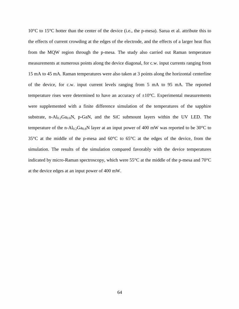
64
10°C to 15°C hotter than the center of the device (i.e., the p-mesa). Sarua et al. attribute this to
the effects of current crowding at the edges of the electrode, and the effects of a larger heat flux
from the MQW region through the p-mesa. The study also carried out Raman temperature
measurements at numerous points along the device diagonal, for c.w. input currents ranging from
15 mA to 45 mA. Raman temperatures were also taken at 3 points along the horizontal centerline
of the device, for c.w. input current levels ranging from 5 mA to 95 mA. The reported
temperature rises were determined to have an accuracy of ±10°C. Experimental measurements
were supplemented with a finite difference simulation of the temperatures of the sapphire
substrate, n-Al0.2Ga0.8N, p-GaN, and the SiC submount layers within the UV LED. The
temperature of the n-Al0.2Ga0.8N layer at an input power of 400 mW was reported to be 30°C to
35°C at the middle of the p-mesa and 60°C to 65°C at the edges of the device, from the
simulation. The results of the simulation compared favorably with the device temperatures
indicated by micro-Raman spectroscopy, which were 55°C at the middle of the p-mesa and 70°C
at the device edges at an input power of 400 mW.
65
Figure 2.11. A temperature contour map over the surface area of the UV LED at a c.w. input
power of 400 mW, measured through Raman thermometry [83].
Wang et al. [84] also investigated the temperature rise of a UV LED using micro-Raman
spectroscopy. The device of interest was an unpackaged UV LED having a die size of 300 µm x
300 µm. The structure of the investigated UV LED consisted of a sapphire growth substrate and
InGaN/AlGaN MQWs between a n-AlGaN region and a p-GaN region. The p contact was
formed by a Ni/Au contact. Micro-Raman spectroscopy was conducted using the 442 nm line of
a He-Cd source, with a laser-spot size limited spatial resolution of 5 µm. Fig. 2.12 shows the
Raman spectra of the UV LED at input current levels between 85 mA and 110 mA. The Raman
spectra in Fig. 2.12 point to a low intensity sapphire A1g peak near 425 cm-1
, and a GaN E2 high
peak near 575 cm-1
. The peak position of the E2 high peak of p-GaN near 575 cm
-1 was used to
measure device temperature. Calibration was first conducted to find the coefficients of fit for the
relationship between temperature and peak shift, and temperature measurements were carried out

66
for c.w. input currents between 50 mA to 110 mA. The device temperature was found to vary
between 27°C to 107°C in the range of input currents investigated.
Figure 2.12. Micro-Raman spectra of the UV LED at different input currents investigated by
Wang et al. [84].
2.2.6 Relevant literature review of Thermoreflectance spectroscopy
Thermoreflectance imaging is an optical metrology technique that produces temperature
maps of a surface based on the change in the reflectivity of the surface as a function of change in
temperature [85]. Thermoreflectance has been widely used The thermoreflectance coefficient
(Cth, which is related to reflectivity R as ΔR(T)/R) is the normalized change in reflection
coefficient, which is only on the order of 10-2
-10-5
/K for most materials under visible
wavelengths. Thus, the acquisition of thermoreflectance data requires a high precision imaging

67
system incorporating a CCD camera with a lock-in amplifier to improve signal amplitude, and a
narrow band noise rejecting filter [86]. Thermoreflectance has been widely used to study
dielectric responses of semiconductors, to study phonon transport in semiconductors in pico-
second scales, and to characterize thermal properties of thin films [85]. The setup of a CCD-
based thermoreflectance setup is shown in Fig. 2.13. Fig. 2.13 shows a CCD camera sensitive to
visible light, and a monochromatic LED light source used for illumination of the sample at an
optimized wavelength. The light reflected back onto the CCD from the sample under heating or
cooling is collected in a phase-locked mode and analyzed to obtain temperature transients of the
sample [85].
Figure 2.13. Setup of a CCD based thermoreflectance microscope [85].

68
Kendig et al. [87] used thermoreflectance imaging to obtain 2D temperature maps of a UV
LED as well as a blue LED in operation. EL and thermoreflectance signals were captured by a
custom 1-megapixel CCD system, capable of a temperature resolution of less than 1°C, and a
time resolution of 25 ns. The devices of interest consisted of a commercial UV LED with 50
separate 280µm diameter active regions in a 2 mm thick plastic encapsulant, and a blue LED
with a 500µm x 500µm active region. Measurement was preceded by calibrating for the
temperature dependence of reflectivity (which is wavelength, surface roughness, and material
dependent). Combined EL and thermoreflectance measurements allows for the evaluation of
temperature maps for the presence of anomalies such as hot-spots as well as the comparison of
temperature map with EL maps, to find light output behavior in regions of interest. It was found
that the thermal map of the UVLED showed a uniform temperature distribution among all the
active regions due to efficient heat spreading in the heat sink, while the EL map showed non-
uniformities in the light output. And, measurements on the blue LED indicated significant
thermal and light output non-uniformities over the device. Thermoreflectance was also used to
find the transient thermal response of the LEDs to a 500 ns current pulse at varying current input
levels. Transient thermal measurements were conducted for different spatial locations across the
die, and the plot of normalized temperature and normalized light output against spatial location
in the device was produced.
2.2.7 Relevant literature review of Network Identification by Deconvolution methods,
and related transient thermal modeling
Farkas et al. [88] investigated high power LEDs through transient electro-thermal and
photometric measurements, as well as thermal simulations. The transient testing method at the

69
focus of this paper has been discussed in previous studies [89-91]. The temperature transient of a
system carries with it information about the thermal properties of the physical structures that
compose the system. The Network Identification by Deconvolution (NID) method employed by
Farkas et al. uses the time constant density of the system to produce the cumulative structure
function (CSF). The CSF is sum of system thermal capacitances in terms of the sum of system
thermal resistances, from the layer of heating to air. Physical discontinuities reflecting the
transition between material layers can be manually identified by peaks in the Differential
Structure Function (DSF), which is the derivative of the CSF with respect to the sum of thermal
resistances [89].
Farkas et al. first offer the example of a green LED subjected to self-heating at an input current
of 400 mA to illustrate the transient analysis method, with the temperature transient being
derived from the change in Vf when measured with a sensing current of 10 mA. The Tj was
derived from a previously calibrated factor for the variation of Vf with Tj. The transient electrical
response of the LED was measured using a thermal transient tester with capability for combined
photometric and radiometric testing. The device under test (DUT) was placed on a temperature
controlled cold plate, inside an integrating sphere where the radiometric flux was recorded along
with the input current and Vf.
The electrical transient was then processed using proprietary software to remove electrical
disturbances and obtain the CSF, which Farkas et al. explain to be a graphical representation of
the one-dimensional thermal resistance-capacitance (RC) network from the LED junction. The
CSF and DSF of the green LED is seen in Fig. 2.14 (a) and (b) respectively. Manually
identifying the regions of the DSF which correspond to physical material boundaries in the
thermal path allows one extract the thermal properties of discrete layers to obtain a compact

70
thermal model of the heat path from the junction to air. The thermal network represented by Fig.
2.14 (a) and (b) has been shown to be divided into three distinct regions – a high thermal
conductivity region A, and two low conductivity regions B and C.
Farkas et al. stress the importance of accounting for power conversion inefficiencies electrical
circuit of the LED, where the input power supplied to the LED is converted into heat in electrical
resistances inside the bulk semiconductor/contact regions of the LED, as well as in resistive
circuit elements in the electrical circuit. The input power is also converted into light through
recombination mechanisms in the LED. Thus, Farkas et al. point to the need for refinement of
the aforementioned compact thermal model (based solely on the input power supplied to the
LED) to include the external and internal quantum efficiencies of the DUT ( and
respectively).
(a) (b)
Figure 2.14. (a) The cumulative structure function of a green LED at a DC input current of 400
mA, and (b) the differential structure function of the green LED at a DC input current of 400 mA
[88].

71
Farkas et al. propose a thermal model with 4 different complexity levels, the simplest being the
case of self-heating at only the junction of the LED along with a constant , and the three
others accounting for self-heating in different parts of the LED’s electrical circuit, and for
different types of control circuitry. In particular, the three complex models are built upon the
basic model, which requires knowledge of the thermal resistance with respect to total input
electrical power (Rthe) the thermal resistance with respect to the input power converted to heat in
the resistance elements (Rthr), as well as the ratio of output power to the input power into the
diode ( ) . More complex models take into account the , and the fact that the power losses
in the electrical circuit are larger for higher input current levels. The Rthe was measured from the
cooling transients of the green LED after being subjected to self-heating at input currents of 100,
200, 400 and 800 mA, and then switching to 10 mA after steady state was reached. The change
in Rthe with input powers was simulated by the four models, using the measured parameters as the
basis of the models. Finally, Farkas et al. contend that simulated models can be extended to a
board level simulation of temperatures in the circuitry and multiple LED junctions in an LED
array at a variety of input current levels.
2.2.8 Principle of Infrared spectroscopy and relevant literature review
IR spectroscopy is an optical thermometry method which measured the radiant emission in the
IR portion of the electromagnetic spectrum from a surface, and is able to produce the 2D
temperature map of the surface based on knowledge of the apparent emissivity of the surface of
interest and the Stefan-Boltzmann law for irradiance from a grey body (which states that J =
εσT4, where J is irradiance, ε is the emissivity, σ is the Stefan-Boltzmann constant and T is the
temperature) [92]. IR spectroscopy is a commonly used method for measuring temperatures of
72
electronic devices under operation, and is particularly advantageous because Si (used as a
submount in most electronics) is transparent to IR. IR spectroscopy it is able to detect high
thermal gradients and temperature maxima and minima on the surface of the electronic device
under test, in real-time. It must be noted here that IR spectroscopy is able to resolve thermal
gradients by measuring the surface temperature of an electronic device under a known
magnification, and known length scale. The total radiation collected by an IR detector includes
components of incident and reflected background radiation, which must first be discounted for
by calibration. Modern IR cameras contain calibration algorithms to account for the effects of
changing background radiation. [93].
IR spectroscopy has become commonplace in the semiconductor industry, and is used to
produce surface temperature maps of a device or an array of devices based on the IR radiation
emitted from the surface, and the knowledge of surface emissivity [94]. Due to the profusion of
high quality handheld IR cameras, IR imaging of electronic components is quick, and may be
used on high power and UV LEDs.
Since the temperature distribution of a surface at different temperatures is deduced from the
calibrated total hemispherical emissivity of the surface, when it is calibrated at a certain
temperature, IR spectroscopy assumes the device of interest to be a grey and diffuse body. Thus,
according to the definition of radiative properties [95], IR spectroscopy also assumes that the
body of interest is an opaque body. For multilayered semiconductor devices, the transmissivity
of various layers must be considered in the interpretation of results, where the thermal response
of the most opaque layer will dominate the temperature measured by IR spectroscopy. The effect
of interfaces between semiconductor layers, where the electromagnetic wave will be partially
reflected and partially transmitted, must also be taken into account [95]. For UV LEDs, the

73
transmissivities of UV grade sapphire substrates (at thicknesses ≤ 1 mm) between room
temperature and 500°C has in the wavelength range of 3-5 µm been measured to be ≥ 0.9 [96] .
Thus, IR spectroscopy of flip chip UV LEDs with sapphire substrates will measure temperature
responses that are dominated by layers underneath the sapphire substrate. Optical properties of
thin, UV grade AlN in the mid-infrared range have been not well investigated in literature. For
more information about optical constants of semiconductor materials and the theory of optical
responses of multilayer systems such as semiconductor superlattices, the reader is directed to
Palik, 1997 [97].
Webb [94] conducts an intensive review of the IR spectroscopy method, including an
explanation of theoretical background noise cancellation algorithms in IR cameras, particularly
when the emissivity of the surface is to be found. The study also includes an extensive list of the
sources of error in an IR measurement (e.g. surfaces with low emissivities causing an
erroneously low temperature reading). Temperature distributions measured from the IR on a
GaAs MESFET for an uncoated (i.e., plain) device with low surface emissivity at the metal
contacts, and a device coated with a thin (3-4 µm) dielectric layer to improve surface emissivity,
were compared. The experimental temperature distribution was also compared with surface
isotherms of the device produced by numerical modeling. It was found that the difference
between IR temperature measurements on the uncoated device, without using image
enhancement methods, and the numerical model was 46%. And, if improved measurement
techniques (i.e., high resolution and improved image processing methods) were used, there was
still a difference of 10% between the uncoated device and the numerical model, deeming the use
of a coating necessary when measuring the temperature of a low emissivity area on a
semiconductor device using IR spectroscopy.

74
CHAPTER 3
EXPERIMENTAL METHODOLOGY FOR INTERNAL DEVICE
TEMPERATURE MEASUREMENTS
This chapter focuses on the instrumentation and experimental methodologies of metrology
techniques that measure the temperature internal to the UV LED, i.e., the Forward Voltage
method, micro-Raman spectroscopy, Infrared spectroscopy, and Electroluminescence
spectroscopy. This chapter also specifies the two types of devices investigated in this study, the
micropixel device and the interdigitated device, in terms of their device structure and packaging.
The locations of temperature measurements in the two types of devices are defined.
3.1 Device structure, electrode geometries and measurement locations of
investigated UV LEDs
Two types of UV LEDs were investigated in this work, the device that had a micropixel
contact geometry, and the device which had an interdigitated electrode geometry. Both types of
devices used in this investigation were supplied by commercial vendors, in their packaged form.
Further modification of the supplied device or package was not performed in this investigation.
3.1.1 Device structure of the micropixel device
The cross-sectional schematic of a micropixel device is shown in Fig. 3.1. The micropixel
devices in this study contained AlxGa1-xN multiple quantum wells (MQWs) with x>0.6, grown on
monolithic sapphire substrates. The active device layers were deposited using pulsed atomic
layer epitaxy (PALE) atop a 10-20 µm thick AlN buffer layer grown using metalorganic hydride

75
vapor phase epitaxy (MOHVPE). A 10 period AlN/ AlxGa1-xN short period superlattice (SPSL)
was grown using PALE between the device active regions and the AlN buffer layer to prevent
epilayer cracking. A 2 µm thick Si-doped n- AlxGa1-xN layer lies adjacent to the short period
superlattice. The MQW region also lies adjacent to a 200Å thick Mg-doped p- AlxGa1-xN
electron blocking layer, followed by p- AlxGa1-xN /p+-GaN hole accumulation layers [39, 98, 99].
Ti/Al/Ti/Au and Ni/Au were used as the n- and p- contact metallization schemes, respectively
[98]. Each of the micropixel devices consisted of an array of 20µm diameter p-contact circular
micropixels, with the n-electrode grid running around the micropixels, as shown in Fig. 3.2 [39].
The devices had an array size of not more than 10x20 micropixels.
Figure 3.1. Cross-sectional schematic of a micropixel device, showing the multilayered
composite device structure.
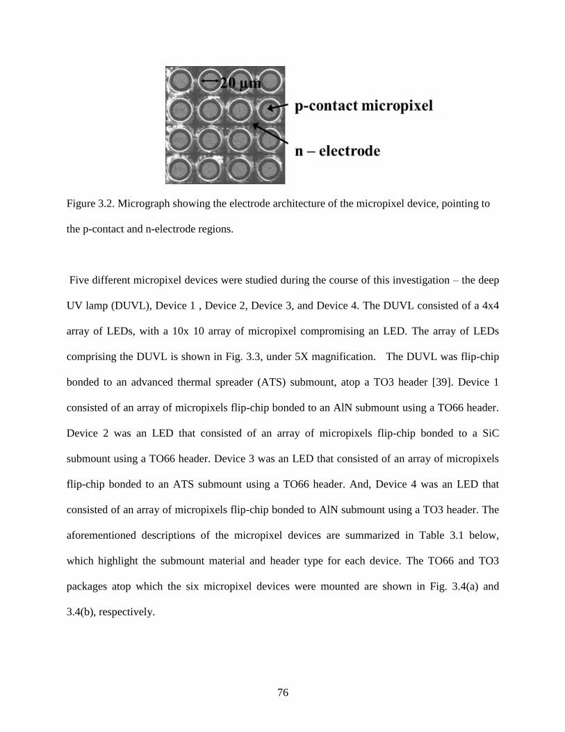
76
Figure 3.2. Micrograph showing the electrode architecture of the micropixel device, pointing to
the p-contact and n-electrode regions.
Five different micropixel devices were studied during the course of this investigation – the deep
UV lamp (DUVL), Device 1 , Device 2, Device 3, and Device 4. The DUVL consisted of a 4x4
array of LEDs, with a 10x 10 array of micropixel compromising an LED. The array of LEDs
comprising the DUVL is shown in Fig. 3.3, under 5X magnification. The DUVL was flip-chip
bonded to an advanced thermal spreader (ATS) submount, atop a TO3 header [39]. Device 1
consisted of an array of micropixels flip-chip bonded to an AlN submount using a TO66 header.
Device 2 was an LED that consisted of an array of micropixels flip-chip bonded to a SiC
submount using a TO66 header. Device 3 was an LED that consisted of an array of micropixels
flip-chip bonded to an ATS submount using a TO66 header. And, Device 4 was an LED that
consisted of an array of micropixels flip-chip bonded to AlN submount using a TO3 header. The
aforementioned descriptions of the micropixel devices are summarized in Table 3.1 below,
which highlight the submount material and header type for each device. The TO66 and TO3
packages atop which the six micropixel devices were mounted are shown in Fig. 3.4(a) and
3.4(b), respectively.

77
Figure 3.3. Micrograph of 4x4 array of 10x10 micropixel LEDs comprising the Deep UV Lamp,
under 5X magnification.
Table 3.1. Table describing the four micropixel UV LED devices investigated in this study.
Device Name Description
Deep UV Lamp
(DUVL)
4x4 array of LED devices atop an ATS submount and TO3
power substrate
Device 1 LED device atop an AlN submount and TO66 power substrate
Device 2 LED device atop a SiC submount and TO66 power substrate
Device 3 LED device atop an ATS submount and TO66 power substrate
Device 4 LED device atop an ATS submount and TO3 power substrate

78
(a) (b)
Figure 3.4. Micropixel devices mounted on (a) a TO66 header and (b) a TO3 header. The device
mounted on the TO3 header is the DUVL.
3.1.2 Locations of Raman measurement of micropixel device
The locations of micro-Raman temperature measurements for micropixel devices, in
relation to the device schematic, are shown in Fig. 3.5 below. As can be seen from Fig. 3.5, four
locations inside the device were studied, namely, Locations I, II, III and IV.
Location I corresponds to the n- AlxGa1-xN layer that lies adjacent to the MQW region, at the
center of the p-mesa micropixel. Location II corresponds to the AlN buffer layer, above the n-
AlxGa1-xN layer, and the AlN/ AlxGa1-xN SPSL, at the p-mesa. Location III corresponds to the
sapphire growth substrate layer, at the p-mesa. Location IV corresponds to the n- AlxGa1-xN
layer, adjacent to the MQW layer, at the center of the n-electrode (equidistant from surrounding
p-mesa micropixels).
All measurement locations were done on the two dimensional geometrical center of the device
geometry, in a region known to have the highest theoretical temperature rise within the device
(with the exception of hotspot regions) based on an analytic heat conduction expressions. For
the DUVL, temperature measurements at Locations I, II and III and IV are discussed in detail.
The temperature measurement measured through the peak position method, for Location I is

79
presented after accounting for the effects of inverse piezoelectric stresses in the n- AlxGa1-xN
layer over the p-mesa. A discussion of the apparent temperature measurements measured through
the peak position method, at Location IV for the DUVL are also presented, without accounting
for the inverse piezoelectric effects in the n- AlxGa1-xN layer over the n-electrode. The
temperatures at Locations II and III are also shown for a micropixel with a hotspot, in the
DUVL. The limitations of measuring temperature in the n- AlxGa1-xN layer in the devices at the
focus of this study, as well as the limitations in correcting for inverse piezoelectric stresses in
the n- AlxGa1-xN layer, are discussed in detail. Temperature measurements for Locations II and
III, i.e., the AlN and sapphire layers over the p-mesa, are presented for Devices 1, 2, 3 and 4.
Figure 3.5. The four locations of micro-Raman measurements in the micropixel device, shown
in relation to the various layers in the device.
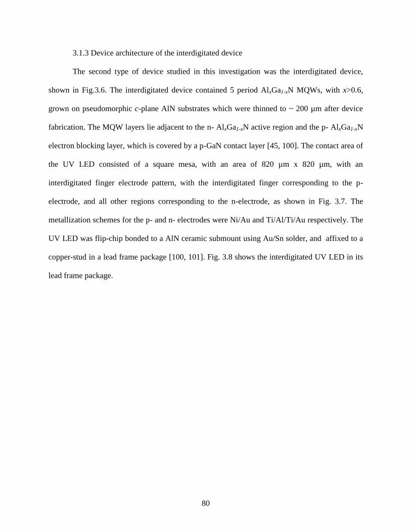
80
3.1.3 Device architecture of the interdigitated device
The second type of device studied in this investigation was the interdigitated device,
shown in Fig.3.6. The interdigitated device contained 5 period AlxGa1-xN MQWs, with x>0.6,
grown on pseudomorphic c-plane AlN substrates which were thinned to ~ 200 µm after device
fabrication. The MQW layers lie adjacent to the n- AlxGa1-xN active region and the p- AlxGa1-xN
electron blocking layer, which is covered by a p-GaN contact layer [45, 100]. The contact area of
the UV LED consisted of a square mesa, with an area of 820 µm x 820 µm, with an
interdigitated finger electrode pattern, with the interdigitated finger corresponding to the p-
electrode, and all other regions corresponding to the n-electrode, as shown in Fig. 3.7. The
metallization schemes for the p- and n- electrodes were Ni/Au and Ti/Al/Ti/Au respectively. The
UV LED was flip-chip bonded to a AlN ceramic submount using Au/Sn solder, and affixed to a
copper-stud in a lead frame package [100, 101]. Fig. 3.8 shows the interdigitated UV LED in its
lead frame package.

81
Figure 3.6. Cross-sectional schematic of an interdigitated device, showing the multilayered
composite device structure.
Figure 3.7. Micrograph showing the interdigitated electrode geometry of the interdigitated
device, depicting the p-mesa and the n-electrode.

82
Figure 3.8. The lead-frame package of the interdigitated device.
3.1.4 Locations of Raman measurement of the interdigitated device
Micro-Raman measurements on the interdigitated devices were conducted at two
locations within the device; the AlN growth substrate layer and the p-GaN contact layer. These
two locations are highlighted in Fig. 3.9, which shows the measurement locations with respect to
the device schematic. The AlN and p-GaN layers, shown in Fig. 3.9, were measured at the edge
of the p-mesa interdigitated finger in the interdigitated device. This location was shown to have
the highest temperature among all other locations, when the 2D temperature map of the device
was generated with the help of IR thermography. Fig. 3.10 shows the IR thermograph of the
interdigitated device, depicting the region of the p-mesa exhibiting highest temperature rise over
the 2D surface of the interdigitated device. It is this region of high temperature on the edge of the
p-mesa, shown in Fig. 3.10, where micro-Raman measurements were taken.
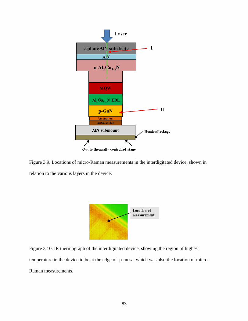
83
Figure 3.9. Locations of micro-Raman measurements in the interdigitated device, shown in
relation to the various layers in the device.
Figure 3.10. IR thermograph of the interdigitated device, showing the region of highest
temperature in the device to be at the edge of p-mesa. which was also the location of micro-
Raman measurements.

84
3.2 Instrumentation, calibration and measurement procedures for micro-Raman
spectroscopy
3.2.1 Raman spectroscopy instrumentation
All micro-Raman experiments were conducted with the 488 nm line of an Ar+ laser and
3000 l/mm diffraction grating, in 180° backscattering geometry with a 50X LR lens. The devices
were studied in c-plane orientation. The resulting Raman spectrum was analyzed with a
Gaussian-Lorentzian fit to find peak parameters of the Stokes peaks of interest. The
commercially available Renishaw InVia Raman microscope was used for all experiments, with a
laser beam diameter limited spatial resolution of ~ 1µm. The Renishaw InVia microscope is seen
in Fig. 3.11 (a) below, and the setup of the device, showing the UV LED with Cu mount affixed
to on a temperature stage underneath the Raman microscope, is seen in Fig. 3.11 (b).
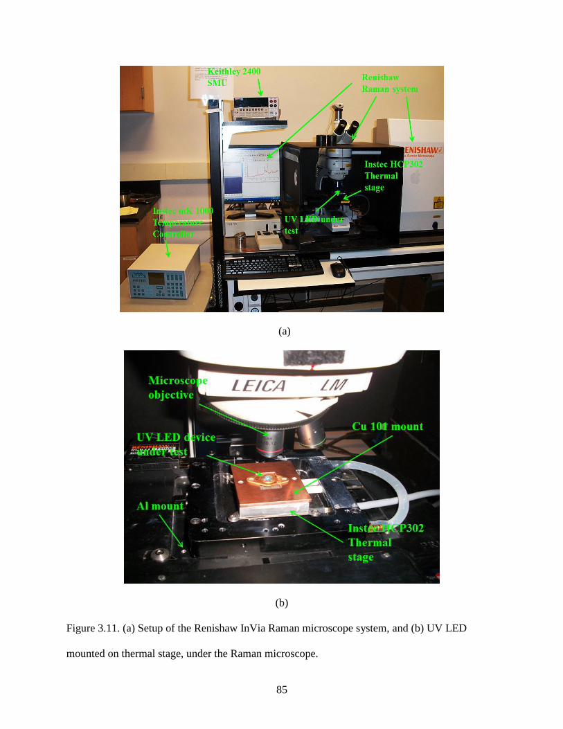
85
(a)
(b)
Figure 3.11. (a) Setup of the Renishaw InVia Raman microscope system, and (b) UV LED
mounted on thermal stage, under the Raman microscope.

86
All power sourcing and electrical measurements were conducted with a Keithley 2400 SMU, in
4 wire configuration. Both the calibration and measurement steps for micro-Raman thermal
metrology were done on a high spatial uniformity Instec HCP302 hotplate with an Instec 7270
mK1000 temperature controller. Devices were affixed onto the hotplate using a 3.18 mm thick
thermally ultra-conductive oxygen-free (Cu 101) cooper mount, using a thin layer of ITW
Chemtronics CW 7270 silicone-free thermal grease at the points of contact between the mount
and the TO or lead-frame package, and between the mount and the thermally controlled stage.
Use of a silicone free thermal grease helps avoid the problems of baking or dry-out (and the
subsequent loss of thermal conductivity) that occurs with silicone based thermal greases on
prolonged exposure to high temperatures. The Instec hotplate was affixed to a custom made 1.58
thick polished aluminum bracket screwed into the microscope stage. Drawings of both the
copper mounts and the aluminum bracket can be referred to in Appendix B and C, respectively.
Fig. 3.12 (a) below shows the copper mount with a UV LED device on a TO66 package atop a
50mm x 60mm copper mount, and Fig. 3.12 (b) shows as 50 mm x 60 mm copper mount, and a
holder with an inner curved surface to hold the lead frame package in place. Fig. 3.12 (a) and (b)
also show threaded holes for attachment of the mount to the hotplate. The mounting procedure
ensured that the device was immobilized during the micro-Raman process.

87
(a) (b)
Figure 3.12.(a) UV LED device with a TO66 package atop a 50mm x 60mm x 3.18mm copper
mount, and (b) UV LED device with a lead frame package atop a 50mm x 60mm x 3.18mm
copper mount with a holder to hold the curved surface of the package in place.
3.2.2. Procedure for accounting for inverse-piezoelectric strain in the peak position
method
As discussed in Chapter 2, the peak shift method in Raman spectroscopy is influenced by
strain in the crystal. In this investigation, temperature measurements conducted in piezoelectric
layers of the UV LED, i.e., the n-AlGaN layer at Location I of the micropixel LED, was
conducted using the Stokes peak position method adjusted for the effects of inverse-piezoelectric
strain. This was done by reverse biasing the device and finding the variation of peak position
with respect to applied voltage across the device. A linear relation, shown in Eq. 3.1 below, was
constructed.
(3.1)
88
In Eq. 3.1, is the peak position due to inverse-piezoelectric stress under reverse bias, is
the peak position in the unbiased device (i.e., at 0 V potential difference across the ends of the
device), is the coefficient of fit the linear relationship, is the intercept of the linear
relationship, and is the absolute value of the potential difference across the ends of the LED.
Using Eq. 3.1, Eq. 2.6 at the piezoelectric layer can be modified to Eq. 3.2 below.
(3.2)
In Eq. 3.2, the peak shift due to temperature rise during device operation has been adjusted for
the effects of peak shift due to inverse-piezoelectric stresses at the potential difference when
the device is forward biased by a voltage .
3.2.3 Procedure for micro-Raman spectroscopy calibrations and measurements
Thermal metrology using micro-Raman spectroscopy was carried out in a two-step
manner, consisting of the calibration step and the measurement step.
(a) Calibration - The calibration step consisted of calibrating for the coefficients of fit in
Eqs 2.6 and 4.2, for peaks of interest. Calibration for the peak position and linewidth methods
was conducted in an unpowered device over a range of known device temperatures, under the
assumption that the evolution of residual stresses did not differ significantly from the evolution
of temperature in the non-piezoelectric layers. The adjustment for inverse-piezoelectric stresses
was done by reverse biasing the device, to remove the effect of thermoelastic stresses, and
finding the variation of peak position with respect to applied voltage across the ends of the
device. Thus, the peak fit coefficients were found for each peak of interest, for the methods.
Micropixel devices were calibrated from stage temperatures of 25°C to 85°C in increments of
15°C. Interdigitated devices were calibrated from stage temperatures of 40°C to 70°C in
89
increments of 10°C.
(b) Measurement - The measurement step consists of first recording the reference peak
position, ωo, of the unpowered device at a known temperature. The device was then supplied a
known DC input power, and the Raman spectrum, which includes the peak of interest, was
recorded for the operational device. Measurement readings for micropixel and interdigitated
devices were taken on a stage temperature of 50°C. The exposure time on the micro-Raman
microscope was regulated such that the intensity of the peaks of interest remained close to
constant throughout the calibration and measurement processes, and a high signal to noise ratio
was achieved. For interdigitated devices, in addition to regulating the exposure time for near-
constant intensity in the peaks of interest, a lengthy exposure time was chosen (~15s per
acquisition) to account for the relatively low intensity of the E2high
mode of p-GaN compared to
the E2high
mode of AlN. This ensured a high signal to noise ratio in the E2high
mode of p-GaN. To
ensure a small experimental uncertainty, each accumulation was composed of between 20 and 25
acquisitions.
3.3 Instrumentation, calibration and measurement procedure for Infrared
spectroscopy
In this study, IR spectroscopy was conducted using a Quantum Focus Instruments (QFI)
InfraScope II. IR microscope, which was equipped with a 256 x 256 element InSb quantum
detector that is sensitive to wavelength between 2 – 5.5 µm, and offers a temperature resolution
of 0.01°C. The QFI Infrascope II is shown in Fig. 3.4 below. Fig. 3.13 shows the IR microscope,
and the location of the LED device atop the temperature controlled stage. The LED device was
mounted atop the thermal stage using ITW Chemtronics CW 7270 silicone-free thermal grease.

90
The thermal stage was mounted on a movable platform, coarsely and finely adjustable in three
dimensions.
Figure 3.13. QFI Infrascope II IR microscope, showing the location of the UV LED on
temperature controlled stage.
The IR thermometry process consists of calibrating the device of interest, before IR
measurements were taken of the powered device. A calibration reading was taken of the
unpowered device at a known temperature, when it was fixed atop a thermal stage. The radiance
emittance of the unpowered device at a known temperature was used to produce a surface
emissivity map of the device after accounting for radiance emittance from background sources.
Then, the device was placed on the thermal stage with at a known temperature, and biased with a
known DC input power. The radiance emittance from the powered device was used to calculate
the absolute temperature of the viewed surface of the powered device at steady state.

91
In this study, the temperature of the thermal stage was maintained at 60°C for calibration as
well as measurement in the IR thermometry measurements for all devices, in order to ensure a
good signal to noise ratio in the response of the quantum detector. All electrical measurements
were conducted using a Keithley 2400 SMU. To facilitate an accurate comparison with micro-
Raman spectroscopy, the regions of temperature rise investigated in the micro-Raman
spectroscopy were the same as the regions of temperature rise investigated through IR
spectroscopy. No pre-treatment of the device surfaces were conducted in this study. Furthermore,
investigations using different magnifications – 1X, 5X and 15X (corresponding to pixel-limited
spatial resolution of 36 µm and 7.2 µm, and a diffraction-limited spatial resolution of 2.9 µm,
respectively) showed no significant differences in the magnitude of temperature rise detected at
the regions of interest in the devices. Ultimately, a 5X magnification was chosen due to its field
of view of 2.37 mm2, which allowed for monitoring of an appropriately large device surface area
for the presence of any thermal anomalies in the device, without compromising spatial resolution
to a great extent. In this work, results of the IR spectroscopy temperature measurement method
are presented for both types of UV LED devices.
3.4 Instrumentation, calibration and measurement procedures for
Electroluminescence (EL) spectroscopy
In this investigation, EL measurements were performed on the DUVL device under c.w.
input power. Spectral characterization of the emission spectrum from the powered device was
conducted using the Ocean Optics Jaz Combo spectrometer module. The device was first placed
on a copper mount affixed to a thermal stage, in a setup identical to the setup used for micro-
Raman spectroscopy. The Jaz spectrometer is equipped with a fiber-optic cable capable of

92
transmission between 200-1000 nm. One end of this cable was secured to the detector of the Jaz
spectrometer, while the other end was secured to a collimating lens, capable of transmitting light
within 200 – 2000 nm. The lens was positioned directly over the frontal area of the device, and
was held in place using a height-adjustable collimating lens holder. The experimental setup of
the EL spectroscopy method is shown in Fig. 3.14, which shows the Jaz spectrometer receiving
optical information from the fiber-optic cable through a collimating lens.
Figure 3.14. Experimental setup of the EL spectroscopy method, showing optical signal
transmission to the spectrometer. The collimating lens is placed in front of the operational LED
in order to characterize EL output.
93
EL measurements were conducted on the devices were mounted on an Instec HPC302 thermal
stage with an Instec mK1000 temperature controller set to a known temperature, biased with a
known d.c. input current and allowed to reach steady state. Electrical sourcing and measurements
were conducted with a Keithley 2400 SMU in 4-wire configuration. The integration time for all
spectral acquisitions was chosen such that no saturation of the spectrum occurred at the
maximum bias within the range of the input powers and all spectral characteristics were
resolvable. The resulting emission spectrum was analyzed using a Gaussian-Lorentzian fit to find
the peak emission wavelength.
EL spectroscopy measurements were taken of the powered UV LED at thermal stage
temperatures between 50°C to 100°C in increments of 10°C, at the same input current level (in
this investigation, the c.w. input current levels studied were 100 mA and 300 mA ). The increase
in Tj from a reference value, taken here as the Tj of the biased LED at an base temperature of
50°C, Tj-50°C, is assumed to be linearly dependent on the shift in peak wavelength. The reference
wavelength in this study is taken to be the peak emission wavelength of the biased LED at a base
temperature of 50°C, - . Therefore, the change in Tj from reference, , can be said to be
related to the change in wavelength from reference, , in Eq. 3.1 below.
(3.1)
In Eq. 3.1, G is the coefficient of linear fit. The change in thus found can be compared with
the results of other metrology methods such as micro-Raman spectroscopy, as will be discussed
in Chapter 4.
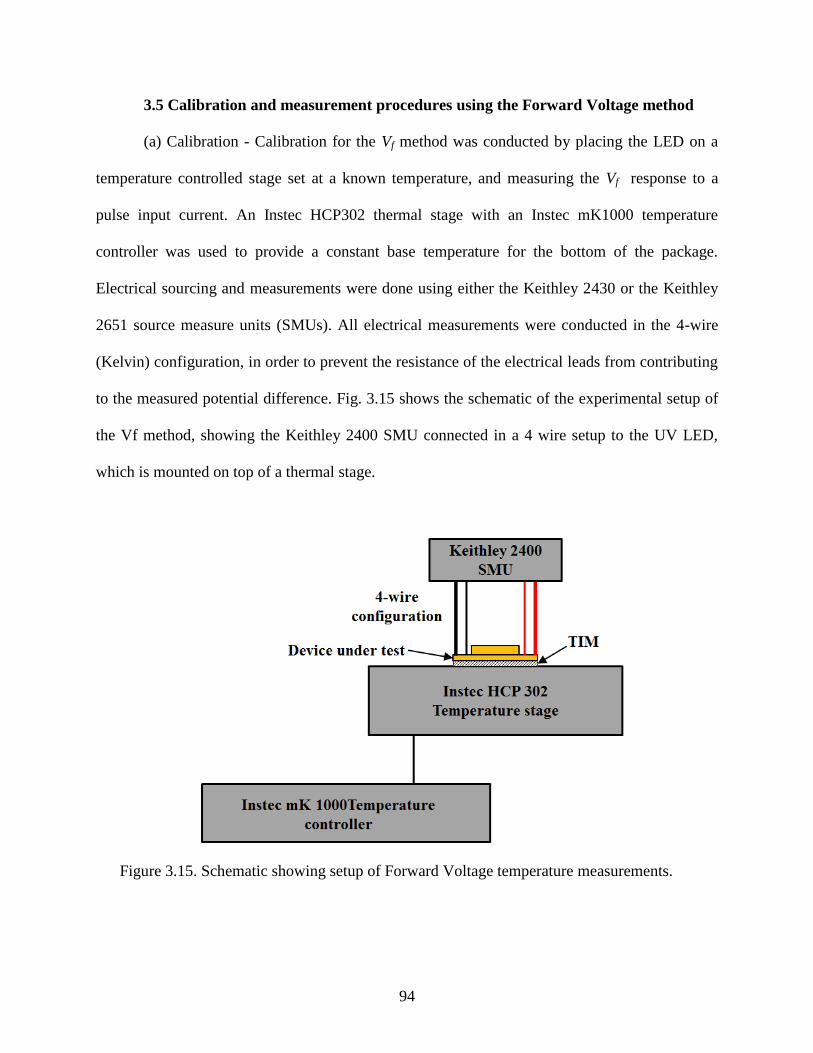
94
3.5 Calibration and measurement procedures using the Forward Voltage method
(a) Calibration - Calibration for the Vf method was conducted by placing the LED on a
temperature controlled stage set at a known temperature, and measuring the Vf response to a
pulse input current. An Instec HCP302 thermal stage with an Instec mK1000 temperature
controller was used to provide a constant base temperature for the bottom of the package.
Electrical sourcing and measurements were done using either the Keithley 2430 or the Keithley
2651 source measure units (SMUs). All electrical measurements were conducted in the 4-wire
(Kelvin) configuration, in order to prevent the resistance of the electrical leads from contributing
to the measured potential difference. Fig. 3.15 shows the schematic of the experimental setup of
the Vf method, showing the Keithley 2400 SMU connected in a 4 wire setup to the UV LED,
which is mounted on top of a thermal stage.
Figure 3.15. Schematic showing setup of Forward Voltage temperature measurements.

95
The LED was allowed to reach thermal equilibrium with the thermal stage (such that the Tj
reaches the temperature of the stage, which is known), and a current pulse at a known level, with
a duty cycle of less than 0.1 % (with a pulse width of less than 1 ms) was then supplied to the
LED, mitigating self- heating in the junction [66]. This process was repeated at a number of
different device temperatures, to obtain the calibration constant A and B (from Eq. 2.1, which
states that Vf = ATj + B) for the Vf method, as shown in Fig. 3.16 below. Fig. 3.16 shows the
linear relationship obtained between the Vf and the Tj, as well as the different input current levels
(20 mA to 80 mA) and junction temperatures 35°C to 65°C) the calibration was conducted for.
Fig. 3.7 shows that at an input current of 100 mA, A is -0.0092 V/°C and B is 9.6 V, with an R2
value of 0.99. In this investigation, all devices were calibrated for junction temperatures between
25°C to 100°C, and for input current levels between 10 mA to 100 mA.
Figure 3.16. Forward voltage and junction temperature calibration curve for an LED at pulsed at
input currents between 20 mA to 100 mA, and for junction temperatures between 35°C to 65°C.

96
(b) Measurement - The measurement procedure involves placing the LED onto a thermal
stage at a known temperature, which was kept between 25°C to 50°C in this investigation, and
allowing the LED to come into thermal equilibrium with the temperature of the thermal stage.
The LED is then supplied with c.w. input current, and allowed to reach steady state. The Vf is
measured across the ends of the LED at steady state, is used to find the Tj based on the
knowledge of A and B from a previous calibration.

97
CHAPTER 4
EXPERIMENTAL RESULTS AND DATA ANALYSIS FOR INTERNAL
DEVICE TEMPERATURE MEASUREMENTS
This chapter presents the experimental results and data analysis from temperature
measurements internal to the device (i.e., micro-Raman, Infrared and Electroluminescence
spectroscopy and the Forward Voltage method). Results are discussed for both micropixel and
interdigitated devices. The temperature distribution inside the device has been examined, and the
presence of vertical temperature differences is established. The temperatures of the material
specific layers of the device have been compared to device junction temperatures, and device
surface temperatures. Results for the Forward Voltage include a discussion on the junction
temperature measurements from the pulse width modulation of visible LEDs.
4.1 Experimental results and data analysis for micropixel devices
4.1.1 The Raman spectrum and an example calibration curve for micropixel devices
Fig. 4.1 shows the Raman spectrum of an unpowered micropixel device at a stage
temperature of 25°C. Four peaks are visible in the Raman spectrum shown in Fig. 4.1. The Eg
modes of sapphire are located ~ 575 cm-1
and at ~ 750 cm-1
. The E2
high mode of n- AlxGa1-xN is
located ~ 591 cm-1
, while the E2
high mode of AlN is located ~ 650 cm
-1. In this work, temperature
measurements conducted on Locations I and IV measure the E2
high modes of n- AlxGa1-xN at the
p-mesa and the n-electrode, respectively. Temperature measurements conducted on Locations II
and III measure the E2
high mode of AlN and the Eg mode of sapphire ~ 750 cm-1
respectively.
The Raman signals from the AlN/ n- AlxGa1-xN SPSL as well as the MQW layers in the

98
micropixel device cannot be detected because of the sub-micron thickness of these layers, which
do not provide a phonon population that is enough to elicit a significant Raman response,
compared to other layers. The asymmetrical shape and linewidth of the n- AlxGa1-xN E2
high peak
shown in Fig. 4.1 can be explained by the spatial correlation model, due to alloy potential
fluctuation (AFP) in substitutional semiconductor alloys [102]. The alloy disorder in n- AlxGa1-
xN leads to translational invariance in the Raman crystal, causing the relaxation of the ⃗ = 0 rule
at the Brillouin zone center (where ⃗ is the phonon wave vector) and resulting in the E2
high mode
of n- AlxGa1-xN which displays AlN-line, or GaN-like behavior, and whose peak position and
linewidth is dependent on the alloy composition, x [103, 104]. The temperature measurements
on Locations I, II, III and IV, were conducted using the stress-independent peak position method,
in micropixels (without a hotspot) for all micropixel devices. The peak position method for
Location I at the DUVL involved a correction for the effects of inverse-piezoelectric stress. Also,
for the DUVL, measurements at the hotspot were conducted using the linewidth method at
Locations II and III.

99
Figure 4.1. Raman spectrum between 514 cm-1
and 775 cm-1
of an unpowered micropixel
device at a thermal stage temperature of 25°C, showing the Raman peaks of interest.
An example of the peak shift calibration curve for the Stokes peak shift for E2
high mode of AlN in
a micropixel device is shown in Fig. 4.2. The calibration curve depicted in Fig. 4.2 shows the
coefficient A in Eq. 2.6 (which states that ) to be -0.0157 cm-1
/°C, and
the R2 to be 0.9987.
500 600 700 8001000
2000
3000
4000
5000
6000
Wavenumber (cm-1
)
Inte
nsi
ty (
a.u
.)
Sapphire Eg
~750 cm-1
Sapphire Eg
~575 cm-1
AlN Ehigh
2
~650 cm-1
n+ - AlGaN E
high
2
~591 cm-1

100
Figure 4.2. Stokes peak shift calibration curve for the E2
high mode of AlN, showing the peak shift
coefficient, for a micropixel device.
4.1.2 Results and analysis from micro-Raman and IR spectroscopies for the Deep UV
Lamp (DUVL)
The coefficient of linear fit, A, from Eq. 2.6, as well as the R2 of fit, for Locations II, III
and IV (i.e., the AlN layer and the sapphire layer, over the p-mesa micropixel, and the n- AlxGa1-
xN layer over the n-electrode) in the DUVL, are shown in Table 4.1 below. For Location I, i.e.,
the n- AlxGa1-xN region over the p-mesa the coefficients for the inverse-piezoelectric stress
adjusted peak shift method, A, D and I from Eq. 3.2, are given in Table 4.2 below. Table 4.2 also
presents the R2 value of the fit from Eq.2.6 and Eq. 3.2, which were the equations used to find A,
and D and I respectively.
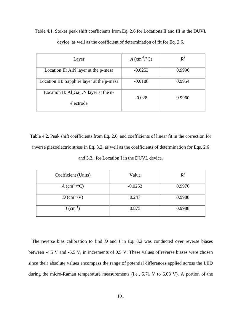
101
Table 4.1. Stokes peak shift coefficients from Eq. 2.6 for Locations II and III in the DUVL
device, as well as the coefficient of determination of fit for Eq. 2.6.
Table 4.2. Peak shift coefficients from Eq. 2.6, and coefficients of linear fit in the correction for
inverse piezoelectric stress in Eq. 3.2, as well as the coefficients of determination for Eqs. 2.6
and 3.2, for Location I in the DUVL device.
The reverse bias calibration to find D and I in Eq. 3.2 was conducted over reverse biases
between -4.5 V and -6.5 V, in increments of 0.5 V. These values of reverse biases were chosen
since their absolute values encompass the range of potential differences applied across the LED
during the micro-Raman temperature measurements (i.e., 5.71 V to 6.08 V). A portion of the
Layer A (cm-1
/°C) R2
Location II: AlN layer at the p-mesa -0.0253 0.9996
Location III: Sapphire layer at the p-mesa -0.0188 0.9954
Location II: AlxGa1-xN layer at the n-
electrode
-0.028 0.9960
Coefficient (Units) Value R2
A (cm-1
/°C) -0.0253 0.9976
D (cm-1
/V) 0.247 0.9988
I (cm-1
) 0.875 0.9988

102
reverse bias IV curve of the DUVL is shown in Fig. 4.15 below. Fig. 4.3 shows the current
response of the DUVL when it is reverse biased with a voltage between 0 V and -10.16 V. Fig.
4.3 also shows the region of the IV curve that contained the reverse bias values used in the
calibration for inverse-piezoelectric stresses. Note here that near a reverse bias level of -4.5 V,
the IV curve in Fig. 4.3 shows a sharp change in slope, pointing to possible non-linearities in the
electric field inside the n- AlxGa1-xN layer beyond this reverse voltage regime, which is
hypothesized to be a possible cause for the non-zero value of the intercept I, found to 0.9 cm-1
from the inverse-piezoelectric stress calibration measurements (as can be seen in Table 4.2).
Figure 4.3. IV curve of the DUVL during reverse bias between voltages of -10.2 V and 0 V.
-1 -0.8 -0.6 -0.4 -0.2 0
x 10-3
-12
-10
-8
-6
-4
-2
0
Current (A)
Vo
lta
ge
(V)

103
Using the coefficients described in Tables 4.1 and 4.2, the temperature measurements of
Locations I, II and and III in the DUVL and are depicted in Fig. 4.4 below. Fig. 4.4 also shows
the results of IR spectroscopy at the center of the p-mesa micropixel, taken from a 5X lens (note
that IR spectroscopy measurements on the micropixel devices did not differ significantly when
taken with a 5X lens and a 15 X lens).
Figure 4.4. The temperature rises with increasing input powers in the sapphire layer (Location
III), the AlN layer (Location II) and the n- AlxGa1-xN layer (Location I) over the p-mesa, in the
DUVL, measured using micro-Raman spectroscopy.
1000 1100 1200 1300 1400 1500 1600 1700 18005
10
15
20
25
30
Input Power (mW)
Tem
per
atu
re R
ise
(°C
)
Micro-Raman: n - AlxGa
1-xN at the p-mesa
Micro-Raman: AlN layer at the p-mesa
Micro-Raman: sapphire layer at the p-mesa
IR spectroscopy
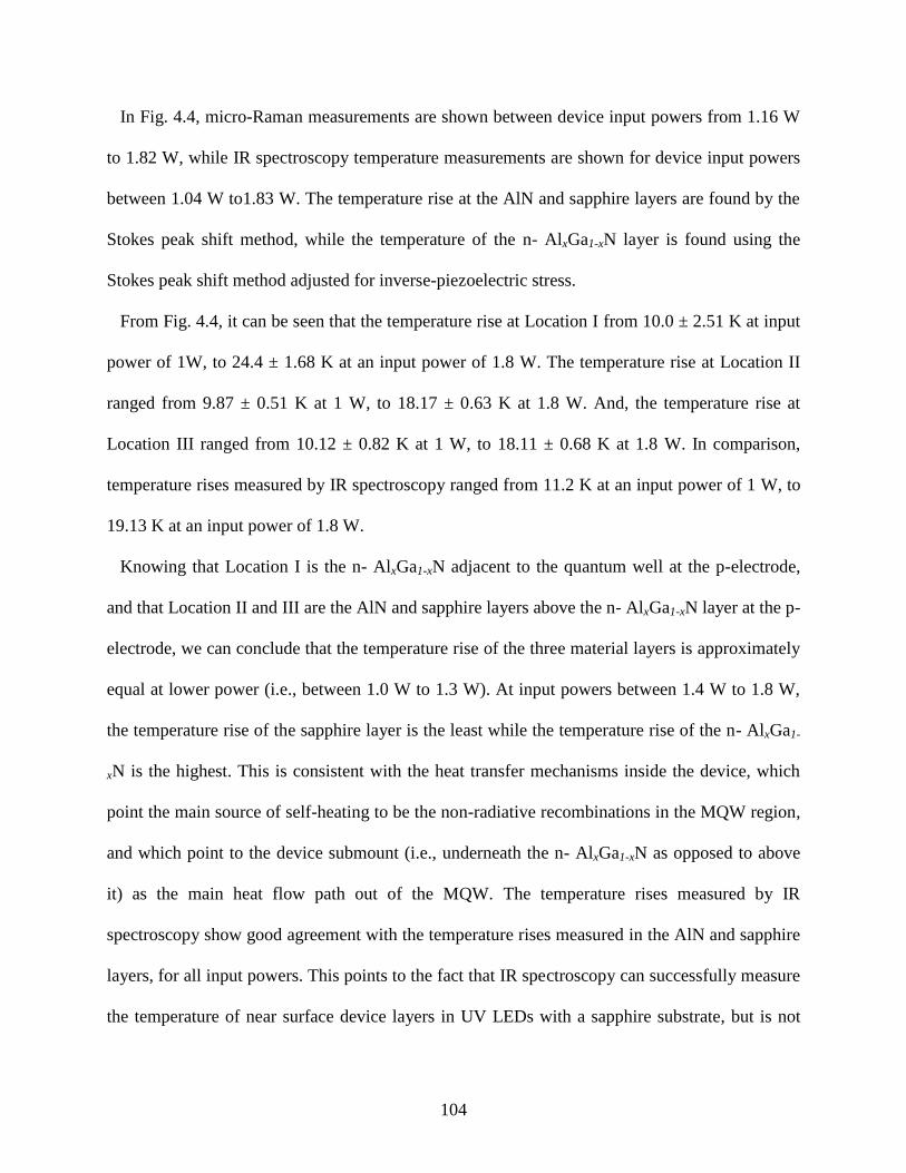
104
In Fig. 4.4, micro-Raman measurements are shown between device input powers from 1.16 W
to 1.82 W, while IR spectroscopy temperature measurements are shown for device input powers
between 1.04 W to1.83 W. The temperature rise at the AlN and sapphire layers are found by the
Stokes peak shift method, while the temperature of the n- AlxGa1-xN layer is found using the
Stokes peak shift method adjusted for inverse-piezoelectric stress.
From Fig. 4.4, it can be seen that the temperature rise at Location I from 10.0 ± 2.51 K at input
power of 1W, to 24.4 ± 1.68 K at an input power of 1.8 W. The temperature rise at Location II
ranged from 9.87 ± 0.51 K at 1 W, to 18.17 ± 0.63 K at 1.8 W. And, the temperature rise at
Location III ranged from 10.12 ± 0.82 K at 1 W, to 18.11 ± 0.68 K at 1.8 W. In comparison,
temperature rises measured by IR spectroscopy ranged from 11.2 K at an input power of 1 W, to
19.13 K at an input power of 1.8 W.
Knowing that Location I is the n- AlxGa1-xN adjacent to the quantum well at the p-electrode,
and that Location II and III are the AlN and sapphire layers above the n- AlxGa1-xN layer at the p-
electrode, we can conclude that the temperature rise of the three material layers is approximately
equal at lower power (i.e., between 1.0 W to 1.3 W). At input powers between 1.4 W to 1.8 W,
the temperature rise of the sapphire layer is the least while the temperature rise of the n- AlxGa1-
xN is the highest. This is consistent with the heat transfer mechanisms inside the device, which
point the main source of self-heating to be the non-radiative recombinations in the MQW region,
and which point to the device submount (i.e., underneath the n- AlxGa1-xN as opposed to above
it) as the main heat flow path out of the MQW. The temperature rises measured by IR
spectroscopy show good agreement with the temperature rises measured in the AlN and sapphire
layers, for all input powers. This points to the fact that IR spectroscopy can successfully measure
the temperature of near surface device layers in UV LEDs with a sapphire substrate, but is not

105
able to measure the temperature of internal device layers. The lack of resolution using IR
spectroscopy may be due to interface effects between the n- AlxGa1-xN layer and the AlN buffer
layer, wherein the IR photons from the n- AlxGa1-xN layer are not able to be transmitted to the
device surface due to reflection at the AlN/ AlxGa1-xN superlattice (SL) layer.
Note that the larger experimental uncertainties in the temperature measurements of the n-
AlxGa1-xN layer in Fig. 4.4 are caused by the inherently larger uncertainty of fit obtained when
mathematically fitting a Gaussian-Lorentzian curve to the asymmetrical n- AlxGa1-xN E2high
peak.
All IR spectroscopy measurement readings documented were calculated from the mean of 100
sample measurements, and the average total uncertainty of all IR spectroscopy measurement for
the devices in this study were approximately 0.1 K, with the exception of hotspot regions in the
devices, where the experimental uncertainty was higher due to the presence of large temperature
gradients on the surface of the device.
In summary, Fig. 4.4 points to the presence of an insignificant thermal difference between the
interior of the device, i.e., the n- AlxGa1-xN layer, and the top of the device growth substrate, i.e.,
the sapphire layer. Fig. 4.4 also validates the temperature rises measured by micro-Raman
spectroscopy with those found with IR spectroscopy of the layers near the device surface, and
finds the two methods to be comparable in their results, for the DUVL device.
The correction for inverse piezoelectric stress was found to be inconclusive for Location IV,
i.e., the n- AlxGa1-xN layer over the n-electrode. This was due to the fact that the coefficient of
linear fit, D, in Eq. 3.2, was found to be equivalent to the experimental uncertainty of curve-
fitting to the n- AlxGa1-xN peak, for Location IV. For the sake of comparison with the
measurements at Location I of the DUVL, Fig. 4.5 shows the apparent temperature rises at
Location IV plotted alongside the temperature rises measured at Location I of the DUVL. Note

106
here that the temperature rises shown for Location IV are not adjusted for inverse piezoelectric
stresses, and represent an apparent or non-physical temperature measurement that is biased by
stress in the n- AlxGa1-xN layer.
Figure 4.5. Raman temperature rises with increasing input power, for the n- AlxGa1-xN layer at
the p-mesa (Location I), and the n-electrode (Location IV) in the DUVL. The temperature rises
at Location I have been corrected for the effect of the inverse piezoelectric stress.
It can be seen from Fig.4.5 that the temperature rises at Location IV extend from 18.3 ± 2.4 K
at an input power of 1.1 W, to 33.7 ± 2.0 K at an input power of 1.9 W. It can also be seen from
Fig. 4.5 that the temperature rise at Location IV is significant higher than the temperature rise at
Location I. For example, while Location IV shows an apparent temperature rise of 18.3 ± 2.4 K
800 1000 1200 1400 1600 1800 20005
10
15
20
25
30
35
40
Input Power (mW)
Tem
per
atu
re R
ise
(°C
)
Micro-Raman: n - AlxGa
1-xN at the p-mesa
Micro-Raman: n - AlxGa
1-xN at the n-electrode

107
at an input power of 1 W, Location I shows a temperature rise of 10.0 ± 2.5 K at input power of
1 W. In short, Fig. 4.5 indicates that the temperature rise of the n- AlxGa1-xN at the p-mesa is
smaller than the n- AlxGa1-xN at the n-electrode. This trend is in direct contrast with the physical
heat transfer mechanisms in the device, which dictate that the majority of joule heating in the
device is produced due to non-radiative recombination at the MQW layers underneath the p-
mesa micropixel, and which do not highlight the n-electrode as a source of heat. Therefore, from
Fig. 4.5, we can conclude that inverse piezoelectric stresses significantly affect the temperature
rises measured through micro-Raman spectroscopy in the n- AlxGa1-xN layer. Furthermore, Fig.
4.5 suggests the characteristic difficulties in accurately calibrating for the inverse piezoelectric
stress effects on an asymmetrical Raman peak.
4.1.3 Results and analysis from micro-Raman and IR spectroscopies for a micropixel
with a hotspot
Mirco-Raman and IR spectroscopy temperature measurements were conducted at a
micropixel with a hotspot, i.e., a micropixel that was not functioning normally, in the DUVL
device. Micro-Raman temperature measurements of the AlN and sapphire layers, and the
temperature rise from IR were compared in order to evaluate their effectiveness in measuring
temperature of the hottest region in the device. Fig. 4.6(a) shows the IR thermograph of the
DUVL device at a magnification of 1X, and points to the LED array where IR spectroscopy was
conducted on a micropixel with a hotspot. The hotspot was measured to discern if Raman
spectroscopy could yield more insight into the location of the hottest point in the LED. Fig.4.6
(a) shows the IR thermograph of the device at a magnification of 5X and Fig. 4.6 (b) also shows
the micropixel with a hotspot, in the DUVL device. The DUVL was biased at an input power of

108
1.8 W in Figs. 4.6(a) and (b). Care was taken to choose the right detector setting in the IR
spectroscopy process, such that saturation of the hotspot temperature did not occur during
measurement.
Micro-Raman temperature measurements at the hotspot regions were conducted at Locations II
and III, using the linewidth method to reduce the impact of thermally induced stresses on the
temperature results. The coefficients of quadratic fit, B and C in Eq. 2.2, along with the R2 of fit
for the sapphire and AlN layers at the micropixel with the hotspot, is shown in Table 4.3.
Temperature rises measured through micro-Raman thermometry, and IR spectroscopy, are seen
in Table 4.4 below.
(a) (b)
Figure 4.6. (a) Micrograph of the DUVL device at a magnification of 1X, showing the LED
array where the micropixel with the hotspot was located, and (b) IR thermograph of the
micropixel with a hotspot, at a magnification of 5X.

109
Table 4.3. Linewidth method coefficients of fit, from Eq. 3.9, for Locations II and III, in the
micropixel with a hotspot, as well as the coefficient of determination of fit for Eq. 3.9.
Table 4.4. Temperature rise at the hotspot, measured by micro-Raman thermography at Locations
II and III, and by IR thermography, at an input power of 400 mW.
Location / Method Temperature Rise (K)
Raman : AlN layer 48.27 ± 6.64
Raman : Sapphire layer 49.22 ± 5.98
IR Thermography - 5x lens 57.07 ± 1.52
Table 4.4 shows the micro-Raman and IR spectroscopy temperature rises at an input power of
400 mW to the DUVL device. As can be seen from Table 4.4, the temperature rise of the AlN
layer and the sapphire layer is comparable to the temperature rise measured by IR thermography,
at the micropixel with a hotspot. Note that temperature measurements at the n- AlxGa1-xN layer,
i.e., Location I, could not be conducted at the hotspot region because of the fact that the
linewidth method, which removes the effects of thermoelastic stress, is coupled with alloy
potential fluctuation for the ternary alloy peak, and thus is dependent on factors other than
temperature. Thus, the location of the hot point within the micropixel could not be determined
Layer B (cm-1
/°C2) C (cm
-1/°C) R
2
Location II: AlN layer at the
p-mesa
8.00E-5 4.41E-3 0.9967
Location III: Sapphire layer at
the p-mesa
7.02E-4 -1.61E-2 0.9963

110
due to the in ability to measure the n- AlxGa1-xN layer which is close to the multiple quantum
wells in the structure.
Thus, from Table 4.4, it can be concluded that the temperature rise of the AlN layer and the
sapphire layer measured by the Raman peak linewdith agree closely with the temperature rise
measured by IR spectroscopy, at regions of high temperature in the micropixel devices.
4.1.4 Data analysis and experimental results for micropixel Devices 1, 2, 3 and 4
Micro-Raman temperature measurements were also conducted on Devices 1, 2, 3 and 4,
at Locations II (the AlN layer at the p-mesa micropixel) and III (the sapphire layer at the p-mesa
micropixel) using the peak shift method. Note that Device 1, 3, 3 and 4 are devices with an AlN
submount with a TO66 header, a SiC submount with a TO66 header, an ATS submount with a
TO66 header, and an AlN submount with a TO3 header. Note that the thermal conductivity, k,
of SiC is greater than that of AlN (kAlN = 285 W/mK and k4H-SiC = 370 W/mK). It is also known
that the ATS submount has a thermal conductivity that is equal or higher thermal conductivity
than that of SiC [105].
The coefficient of linearity, A, from Eq. 2.6, for Locations II and III for the four devices are
given in Table 4.5 below.

111
Table 4.5. Micro-Raman peak shift coefficients for the AlN and sapphire layers (Locations II and
III) in the micropixel Devices 1, 2, 3 and 4, from Eq. 2.6, as well as the R2 value of fit.
Device Location A (cm-1
/°C) R2
Device 1
Location II: AlN layer at the p-mesa -0.0157 0.9987
Location III: Sapphire layer at the p-mesa -0.0139 0.9933
Device 2
Location II: AlN layer at the p-mesa -0.0154 0.9983
Location III: Sapphire layer at the p-mesa -0.0186 0.9935
Device 3
Location II: AlN layer at the p-mesa -0.0139 0.9976
Location III: Sapphire layer at the p-mesa -0.0178 0.9948
Device 4
Location II: AlN layer at the p-mesa -0.0153 0.9977
Location III: Sapphire layer at the p-mesa -0.0188 0.9954
Fig. 4.7 shows the temperature rises measured by micro-Raman spectroscopy at Locations II
and III (i.e., the AlN layer and the sapphire layer) for Device 1. For comparison with micro-
Raman measurements, IR spectroscopy measurements are also shown on the same graph. In
Device 1, the temperature rises at Location II extend from 9.14 ± 0.23 K at a device input power
of 360 mW, to 20.78 ± 0.3 K at a device input power of 690 mW. The temperature rise at
Location III spans between 6.48 ± 1.33 K at an input power of 360 mW, to 19.8 ± 1.6 K at an
input power of 690 mW. The temperature rise derived from IR thermography extended from 8.76
K at an input power of 360 mW, to 14 K, at an input power of 640 mW. From Fig. 4.7, it can be
seen that the temperature rises at the AlN layer and the sapphire layer agree well with each other,
and that the temperature rises measured by IR spectroscopy are reasonably similar to the

112
temperature rise measured by micro-Raman spectroscopy. This points to the fact that
temperature differences between the AlN and the sapphire layer are very small in Device 1 (at
the powers investigated), and that IR spectroscopy can successfully resolve the temperature of
near surface layers in Device 1.
Figure 4.7. Temperature rises in the AlN layer and the sapphire layer, measured by Micro-
Raman thermography, and the temperature rise measured by IR thermography, with increasing
input powers, for Device 1.
Fig. 4.8 shows the temperature rises, measured by micro-Raman spectroscopy for Locations II
and III, and temperature rises measured by IR spectroscopy in Device 2. In Device 2, the
temperature rise measured by micro-Raman spectroscopy extends from 5.84 ± 0.23 K at 460
300 400 500 600 700 8000
5
10
15
20
25
30
Input Power (mW)
Tem
per
atu
re R
ise
(°C
)
IR thermography
Micro-Raman : AlN layer
Micro-Raman: Sapphire layer

113
mW, to 14.9 ± 0.7 K at 690 mW at Location II. And, the temperature rise extends from 5.90 ±
0.57 K at 460 mW, to 15.6 ± 1.3 K at 690 mW , at Location III. The temperature rise from IR
spectroscopy extends from 10.5 K at 460 mW, and 15.5 K at 690 mW. From Fig. 4.8, it can be
seen that the temperatures in the AlN and the sapphire layer at the p-mesa, for Device 2, agree
well with each other. It can also be seen that in general, the temperature rises predicted my
micro-Raman are generally comparable to those predicted by IR spectroscopy – with the
difference between the two methods decreasing at higher powers (i.e., higher temperatures).
Figure 4.8. Temperature rises in the AlN layer and the sapphire layer, measured by Micro-
Raman thermography, and the temperature rise measured by IR thermography, with increasing
input powers, for Device 2.
400 500 600 700 7500
5
10
15
20
25
30
Input Power (mW)
Tem
per
atu
re R
ise
(°C
)
IR Spectroscopy
Micro-Raman: AlN layer
Micro-Raman: Sapphire layer
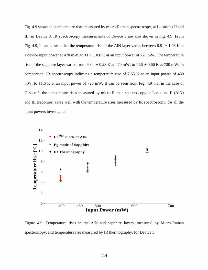
114
Fig. 4.9 shows the temperature rises measured by micro-Raman spectroscopy, at Locations II and
III, in Device 3. IR spectroscopy measurements of Device 3 are also shown in Fig. 4.9. From
Fig. 4.9, it can be seen that the temperature rise of the AlN layer varies between 6.81 ± 1.03 K at
a device input power at 470 mW, to 11.7 ± 0.6 K at an input power of 720 mW. The temperature
rise of the sapphire layer varied from 6.34 ± 0.23 K at 470 mW, to 11.9 ± 0.66 K at 720 mW. In
comparison, IR spectroscopy indicates a temperature rise of 7.65 K at an input power of 480
mW, to 11.6 K at an input power of 720 mW. It can be seen from Fig. 4.9 that in the case of
Device 3, the temperature rises measured by micro-Raman spectroscopy at Locations II (AlN)
and III (sapphire) agree well with the temperature rises measured by IR spectroscopy, for all the
input powers investigated.
Figure 4.9. Temperature rises in the AlN and sapphire layers, measured by Micro-Raman
spectroscopy, and temperature rise measured by IR thermography, for Device 3.
450400 500 600 7007000
2
4
6
8
10
12
14
Input Power (mW)
Tem
per
atu
re R
ise
(°C
)
E2high
mode of AlN
Eg mode of Sapphire
IR Thermography

115
It can be seen that Device 1 (AlN submount) has a higher temperature rise during device
operation, than Device 3 (ATS submount), as measured by IR and micro-Raman. For example, at
an input power of 445 mW, the micro-Raman temperature rises of Device 1 at Locations II and
III are 16.2 K and 8.6 K, respectively. In comparison, Device III shows a temperature rise at
Location II and III of 6.81 K and 6.34 K, respectively, at 470 mW.
It can also be seen that the temperature rise of Device II (SiC submount) is comparable to the
temperature rise of Device III (ATS submount). For example, at an input power of 427 mW, the
temperature rise at Locations II and III in Device 2 are 5.84 K and 5.90 K , respectively. This
compares to a temperature rise of 6.81 K and 6.34 K in Location II and III, respectively, at an
input power of 470 mW for Device 3.
It can thus be concluded that the thermal conductivity of the submount significantly effects the
temperature rise of the device, and that in a well-functioning device, the temperature rise in the
near-surface device layers measured by Raman spectroscopy agree with the temperature rise
measured by IR.
IR spectroscopy conducted on Device 4 led to the discovery of temperature differences on the
surface of the device. Fig. 4.10 below shows the IR thermography, conducted after micro-Raman
measurement, at 5X magnification, of a portion of the device which included the region of
micro-Raman measurements, i.e., the 2D geometrical center of the device. The uneven
temperature distribution seen in Fig. 4.10 (in which the device is shown at an input power of 630
mW) points to the fact that the IR thermography measurements on Device 4 are not directly
comparable to micro-Raman measurements, since they no longer reflect the largest temperature
rise in the device. Thus, in this work, only micro-Raman measurements on Device 4 are
discussed.

116
Figue 4.10. IR thermograph of Device 4 at a magnification of 5X showing horizontal
temperature differences on the surface of the device.
Fig. 4.11 shows the micro-Raman temperature rises in Locations II and III, for Device 4. From
Fig. 4.11, we can see that the temperature rise in the AlN layer in Device 4 extends from 9.49 ±
0.36 K for an input power of 440 mW, to 12.8 ± 0.4 K at an input power of 640 mW. In contrast,
the temperature rise in the sapphire layer extends from 2.66 ± 0.50 K at an input power of 440
mW, to 4.26 ± 0.60 K at an input power of 640 mW. Thus, Fig. 4.11 demonstrates the presence
of a vertical temperature difference between the AlN and sapphire layers of the device. This
demonstrates the fact that micro-Raman spectroscopy is able to discern for vertical temperature
differences between internal device layers in the LED, and is able to resolve internal temperature
information that cannot be found using IR spectroscopy. However, IR spectroscopy is helpful in
providing a convenient thermal overview in a large surface area of the device, aiding in
preliminary studies before more detailed thermal analysis.
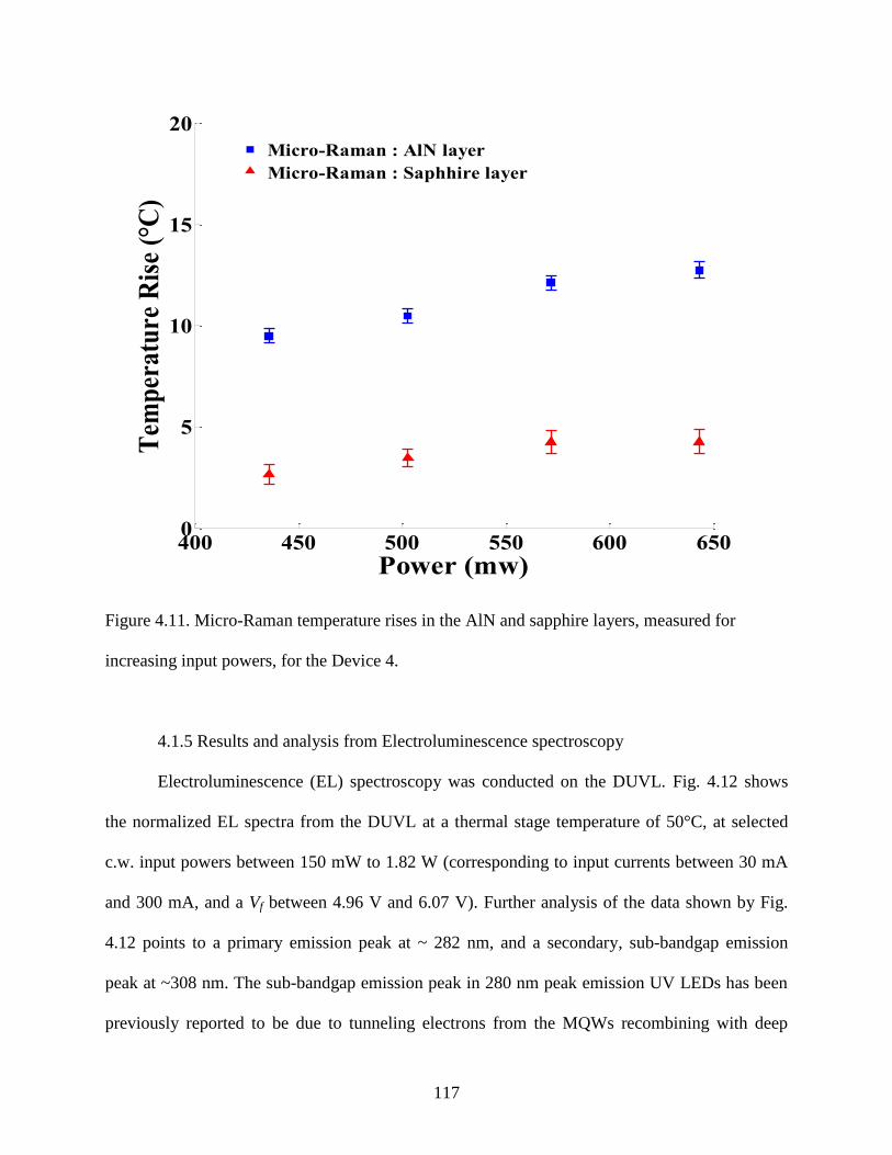
117
Figure 4.11. Micro-Raman temperature rises in the AlN and sapphire layers, measured for
increasing input powers, for the Device 4.
4.1.5 Results and analysis from Electroluminescence spectroscopy
Electroluminescence (EL) spectroscopy was conducted on the DUVL. Fig. 4.12 shows
the normalized EL spectra from the DUVL at a thermal stage temperature of 50°C, at selected
c.w. input powers between 150 mW to 1.82 W (corresponding to input currents between 30 mA
and 300 mA, and a Vf between 4.96 V and 6.07 V). Further analysis of the data shown by Fig.
4.12 points to a primary emission peak at ~ 282 nm, and a secondary, sub-bandgap emission
peak at ~308 nm. The sub-bandgap emission peak in 280 nm peak emission UV LEDs has been
previously reported to be due to tunneling electrons from the MQWs recombining with deep
400 450 500 550 600 6500
5
10
15
20
Power (mw)
Tem
per
atu
re R
ise
(°C
)
Micro-Raman : AlN layer
Micro-Raman : Saphhire layer

118
levels in the p-AlGaN and p-GaN layers[106]. Approaches to alleviate the secondary emission
peak include deepening of the MQW region to prevent electron leakage, and increasing the
thickness and mole fraction of p-doped electron blocking layers [106, 107].
Figure 4.12. EL spectra from the DUVL at a stage temperature of 50°C, at selected c.w. input
powers between 149 mW to 1.82 W.
In Fig. 4.12, the secondary emission peak ranges in intensity from 3.6% to 7.6% of the
intensity of the primary emission peak at 1.82 W. Fig. 4.12 also shows the increase of emission
primary peak intensity with increasing c.w. input power, as well as the saturation of increase in
intensity that takes place at higher c.w. input powers. Fig. 4.12 also reveals a red shift of the
emission peak wavelength that takes place with increasing input powers ; the primary emission
peak shifts from 281.7 nm at an input power of 150 mW, to 282 nm at an input power of 1.82 W.
250 275 300 325 350 375 4000
0.1
0.2
0.3
0.4
0.5
0.6
0.7
0.8
0.9
1
Wavelength (nm)
Norm
ali
zed
In
ten
sity
(%
)
30 mA (~149 mW) to 300mA(1.84W) c.w. biasPeak emmision ~282.01 nm

119
In order to investigate this phenomenon, EL measurements were performed on the DUVL at a
c.w. input current of 300 mA (corresponding to an input power of 1.82 mW, and Vf of 6.07 V,
when on a thermal stage at 50°C), at stage temperatures between 50-100°C. It is assumed that the
temperature rise of the junction from ambient remains the same for a particular c.w. input
current, at different ambient temperatures. Under this assumption, changing the ambient
temperature will change the absolute temperature of the junction. Figure 4.13 shows a plot of
against , for the DUVL at an input current of 300 mA. A linear fit was performed between the
two variables, with the resulting of fit being ≥0.99. The red shift of the emission peak
wavelength, for a unit increase in Tj, i.e., the coefficient G in Eq. 3.1, was thus found to be
0.0185 nm/°C.
Figure 4.13. Shift in emission peak wavelength plotted against the change in junction
temperature, for the DUVL device at an input current of 300 mA.
y = 0.0185x - 0.0114
R² = 0.9989
0
0.2
0.4
0.6
0.8
1
0 20 40 60
Δλ
(nm
)
ΔTj ( C)

120
The red-shift displayed by relationship in Fig. 4.13 is also seen in the EL spectrum of the
DUVL in Fig. 4.14, which shows the EL spectra of the DUVL at an input current of 300 mA and
at thermal stage temperature of 60°C to 100° C. The red shift of the peak emission wavelength
can be seen with increasing junction temperature, and the EL intensity decreases along with
widening of the FWHM of the EL peak.
Figure 4.14. Emission spectra of the DUVL device at an input current of 300 mA, at stage
temperatures of 60°C, 80°C, 100°C.
EL measurements of emission spectra were also taken with the DUVL on a thermally
controlled stage of 50°C, at c.w. input powers of 1.2 W (i.e., corresponding to an input current of
200 mA and a Vf of 5.83 V), 1.50 W (corresponding to an input current of 250 mA and a Vf of
5.99 V) and 1.8 W (corresponding to an input current of 300 mA and a Vf of 6.07 V). The rise in
240 260 280 300 320 340 360 380 4000
0.1
0.2
0.3
0.4
0.5
0.6
0.7
0.8
0.9
1
1.1
1.2
Wavelength (nm)
Norm
ali
zed
In
ten
sity
(a.u
.)
60°C
80°C
100°C
Red Shift of peak emission
wavelength and decrease in
emmision intensity
Increase in FWHM

121
Tj of the DUVL from the temperature of the junction at 1.2 W (and on a 50°C stage) was deduced
by Eq. 3.1 with G =0.0185 nm/°C. The , the rise in Tj , was compared to the rise in
temperature of Location I of the DUVL, at biases of 1.5 W and 1.8 W, as measured by micro-
Raman spectroscopy using the peak position method corrected for the effects of inverse-
piezoelectric stress. Note here that Location I corresponds to the n+ - AlxGa1-xN layer over the p-
mesa micropixel in a non-hotspot region, i.e., in the layer that is adjacent to the MQW and
closest to it in the vertical direction. Table 4.6 shows a comparison of temperature measurements
from the micro-Raman and EL spectroscopies.
Table 4.6. Comparison of temperature measured by EL spectroscopy and micro-Raman
spectroscopy on Location I of the DUVL
Input
Power (W)
EL
Meaurement
ΔTj (°C)
Raman
Measurement of
Location I (°C)
1.17 0 0
1.50 3.24 ± 1.86 4.94 ± 3.62
1.82 5.41 ± 2.51 11.1 ± 3.2
It can be seen from Table 4.6, that the temperature rises from EL spectroscopy and micro-
Raman spectroscopy are comparable to each other at the input powers examined. The ability to
use EL as a thermal metrology tool to measure the of the UV LED, from a reference Tj when
the device is under bias, opens the potential for exploration of future thermal metrology utilizing
the change in wavelength during c.w. operation of the device. EL spectroscopy has the additional

122
advantage of displaying characteristics of device degradation during spectroscopic
measurements, e.g., presence of shoulder or secondary emission peaks and loss of optical power,
which can be used as a convenient tool to study the effects on aging of UV LEDs [70].
4.1.6. Results and analysis from the Forward Voltage method
The Vf method was conducted on Devices 2 and 3 (micropixel devices having an SiC
submount, and an ATS submount, respectively). The Vf method calibration for Device 2 was
conducted over input currents between 10 mA to 25 mA, in intervals of 5 mA, and for
temperatures between 40°C and 100°C in 15°C intervals. Fig. 4.15 shows the calibration curve of
Device 2, showing the variation of Vf with temperature at different input currents. The average
value of the coefficient A (from Eq. 2.1) for the input currents investigated is -3.5 mV/°C, and
the value of B (from Eq. 2.1) varies from 6.02 V at 10 mA to 6.44 V at 25 mA. Measurements
using the Vf method were conducted on a stage temperature of 40°C.
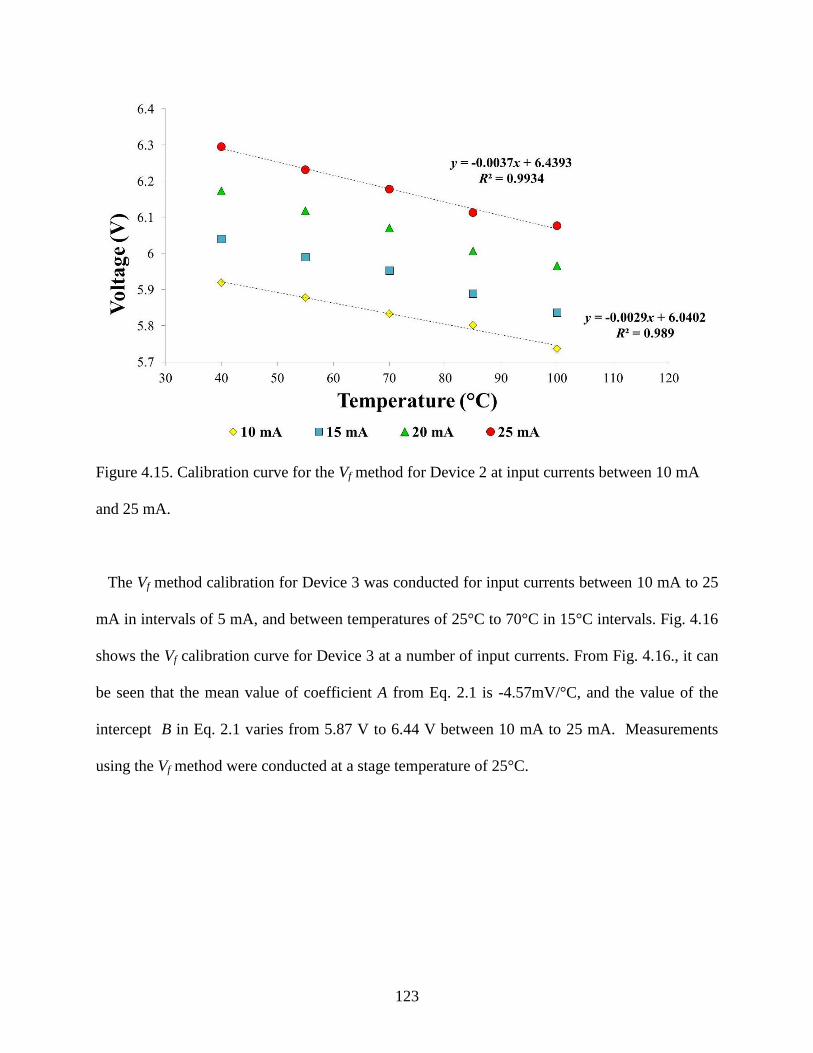
123
Figure 4.15. Calibration curve for the Vf method for Device 2 at input currents between 10 mA
and 25 mA.
The Vf method calibration for Device 3 was conducted for input currents between 10 mA to 25
mA in intervals of 5 mA, and between temperatures of 25°C to 70°C in 15°C intervals. Fig. 4.16
shows the Vf calibration curve for Device 3 at a number of input currents. From Fig. 4.16., it can
be seen that the mean value of coefficient A from Eq. 2.1 is -4.57mV/°C, and the value of the
intercept B in Eq. 2.1 varies from 5.87 V to 6.44 V between 10 mA to 25 mA. Measurements
using the Vf method were conducted at a stage temperature of 25°C.

124
Figure 4.16. Calibration curve for the Vf method for Device 3 at input currents between 10 mA
and 25 mA.
The average change in Vf per degree rise in Tj for Devices 2 and 3, across input currents levels
calibrated for between 10 mA and 25 mA , are summarized in Table 4.7 below.
Table 4.7. Vf method calibration coefficients from Eq. 2.1 for the micropixel devices.
Device Name A (mV/°C)
Device 2 -3.50
Device 3 -4.57
Fig. 4.17 below shows the results of Tj measurements using the Vf method, for Devices 2 and 3.
Measurements on Device 2 were conducted between input powers of 60 mW (corresponding to

125
an input current of 10 mA, and a Vf of 5.84 V) and 160 mW (corresponding to an input current of
25 mA and a Vf of 6.21 V). Measurements on Device 3 were conducted between input powers of
60 mW (corresponding to an input current of 10 mA and a Vf of 5.69 V) and 160 mW
(corresponding to an input current of 25 mA and a Vf of 6.18A).
As can be seen from Fig. 4.17, Device 2 shows a larger junction temperature rise, over the
range of input powers, than Device 3. The temperature rise for Device 2 varies from 28.1 °C at
58.4 mW to 40.3 °C at 155 mW. Conversely, the temperature rise for Device 3 varies from 18.2
°C at 56.9 mW to 25.4 °C at 155 mW. The larger temperature rise for Device 2 is consistent with
the fact that thermal conductivity of SiC, which is the material of Device 2’s submount, is equal
to or lower than the ATS material that comprises Device 3’s submount. The total uncertainty for
all reported measurements is approximately 3°C, limited mainly by the uncertainty of the SMU
reading and the magnitude of the measured Vf. The non-linearity of the temperature vs. input
power curves for Devices 2 and 3 shown in Fig. 4.17 may be explained by changing device
series resistance as the UV LED degrades with increasing input current, which effects the Vf and
the dVf /dT of the LED, as outlined in Section 2.2.

126
Figure 4.17. Junction temperature rise with increasing input power for micropixel devices,
measured using the Vf method.
4.1.7. Summary conclusions from internal temperature measurements of micropixel
devices
The several internal temperature measurements on micropixel LEDs conducted in Section
4.1 point to the unique ability of Raman spectroscopy to provide material specific temperature
data. IR spectroscopy, on the other hand, can provide an overview of thermal phenomena at the
device surface. Using these two methods, the role of the thermal conductivity of the submount in
device temperature rise is explored. Micro-Raman and IR spectroscopy are also used in Section
4.1 to measure the temperatures at hotspots in a non-functional micropixel, and to probe for
horizontal and vertical temperature distributions The Forward Voltage method is influenced by
60 100 140 16015
20
25
30
35
40
45
Power (mW)
Ju
nct
ion
Tem
per
atu
re R
ise
(°C
)
Device 2
Device 3
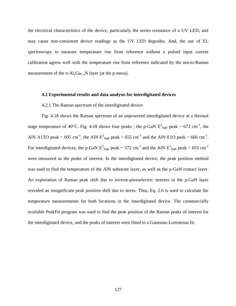
127
the electrical characteristics of the device, particularly the series resistance of a UV LED, and
may cause non-consistent device readings as the UV LED degrades. And, the use of EL
spectroscopy to measure temperature rise from reference without a pulsed input current
calibration agress well with the temperature rise from reference indicated by the micro-Raman
measurement of the n-AlxGa1-xN layer (at the p-mesa).
4.2 Experimental results and data analysis for interdigitated devices
4.2.1 The Raman spectrum of the interdigitated device
Fig. 4.18 shows the Raman spectrum of an unpowered interdigitated device at a thermal
stage temperature of 40°C. Fig. 4.18 shows four peaks ; the p-GaN E2
high peak ~ 672 cm-1
, the
AlN A1TO peak ~ 605 cm-1
, the AlN E2
high peak ~ 655 cm-1
and the AlN E1O peak ~ 666 cm-1
.
For interdigitated devices, the p-GaN E2
high peak ~ 572 cm-1
and the AlN E2
high peak ~ 655 cm-1
were measured as the peaks of interest. In the interdigitated device, the peak position method
was used to find the temperature of the AlN substrate layer, as well as the p-GaN contact layer.
An exploration of Raman peak shift due to inverse-piezoelectric stresses in the p-GaN layer
revealed an insignificant peak position shift due to stress. Thus, Eq. 2.6 is used to calculate the
temperature measurements for both locations in the interdigitated device. The commercially
available PeakFit program was used to find the peak position of the Raman peaks of interest for
the interdigitated device, and the peaks of interest were fitted to a Gaussian-Lorentzian fit.
128
Figure 4.18. Raman spectrum between 566 cm-1
and 672 cm-1
, of an unpowered interdigitated
device, at a thermal stage temperature of 40°C.
4.2.2 Results and analysis from the micro-Raman and Infrared spectroscopies
Table 4.8 below shows the coefficient of linear fit, A, in Eq. 2.6 as well as the R2 value of
fit, used in the peak shift method in the micro-Raman thermometry measurements of the AlN
growth substrate layer and the p-GaN contact layer, in the interdigitated devices .
550 575 600 625 650 6750
1.5
3
4.5
6
7.5
910.1
x 104
Wavenumber (cm-1
)
Inte
nsi
ty (
a.u
.)
AlN A1TO
~605 cm-1
AlN
E1TO
~666
cm-1
AlN Ehigh
2
~655 cm-1
GaN Ehigh
2
~572 cm-1

129
Table 4.8. Micro-Raman peak shift coefficients from Eq. 2.6 for the AlN and p-GaN layers in the
interdigitated device, along with the R2 of fit.
The peak fits shown in Table 4.8 were used to derive the micro-Raman temperature rises shown
in Fig. 4.19 below. Fig. 4.19 shows the temperature rises at the AlN layer and the p-GaN layer
measured through micro-Raman thermometry. For comparison with micro-Raman
measurements, Fig. 4.19 also includes the IR spectroscopy measurements of the interdigitated
device, as well as measurements of the same.
Layer A (cm-1
/°C) R2
AlN growth substrate layer -0.0221 0.9953
p-GaN contact layer -0.0459 0.9960

130
Figure 4.19. Temperature rises for various input powers, for the interdigitated device, in the p-
GaN and AlN layers measured through micro-Raman spectroscopy, and from IR spectroscopy
and the Forward Voltage Method. The inset shows the cross sectional schematic of the
interdigitated device pointing to measurement locations.
From Fig. 4.19, it can be seen that the temperature of the AlN growth substrate extends
between 8.22 ± 0.86 K at an input power of 430 mW, to 15.4 ± 0.7 K at an input power of 750
mW. Conversely, the temperature rise of the p-GaN contact layer extends between 3.38 ± 0.32 K
at an input power of 430 mW, to 8.50 ± 0.46 K at an input power of 750 mW. The temperature
rise of the interdigitated device measured through IR spectroscopy varied between 1.38 K at an

131
input power of 130 mW to 8.17 K at an input power of 780 mW. And, results of the method
indicate the junction temperature of the device to be between 10.2 ± 1.9 K at an input power of
430 mW and 27.6 ± 3.3 K at an input power of 750 mW.
Fig. 4.19 shows clear differences between the temperature rises measured by each method of
thermometry. First of all, a vertical temperature difference is seen between the AlN growth
substrate and the p-GaN contact layer at all input power levels. This is consistent with the
physical mechanisms of heat transfer in the flip-chip device, as the heat produced in the MQW
layer is primarily conducted out of the submount and into the power substrate, pointing to a
larger temperature difference between the MQW layer and the p-GaN contact layer compared to
the temperature difference between the MQW layer and the AlN growth substrate. As the MQW
is the hottest layer in the composite device, it is consistent with reasoning that the p-GaN layer
was found to have a lower temperature rise than the AlN layer.
From Fig. 4.19, it is also apparent that although the temperature rises measured through IR
spectroscopy agree well with the temperature rises measured in the p-GaN layer through micro-
Raman spectroscopy, IR spectroscopy is not able to resolve the temperature of the AlN layer.
This may be due to the fact that the AlN layer could be sufficiently transmissive to allow the
temperatures from layers below it to dominate in the IR thermograph. The decreased spatial
resolution of the IR camera (7.2µm) compared to the high resolution of the Raman microscope
(~ 1µm) may also contribute to inaccurate measurements using IR spectroscopy, in areas of the
device where large temperature differences exist (such as the edge of the p-mesa). On the other
hand, the junction temperature measured by the method shows a temperature rise that is
greater than the temperature rise measured by IR or micro-Raman spectroscopy for a particular
input power. Again, this is consistent with the fact that the method measures the lattice

132
temperature at the junction of the powered device [58]. As the junction is the theoretical region
of highest temperature in the device, due to self-heating during non-radiative recombination, the
temperature rises determined by the method are sensible.
However, the differences in temperature rises shown by the method and the micro-Raman
method raise the question of the practicality of temperature measurements conducted by the
method, for thermal management of the UV LED. The temperature measured by the method is
affected by the contribution of the series resistance at the Ohmic contacts, and in the bulk
semiconductor regions of the LED (including the effects of current crowding), to the and
[58]. The series resistance of the LED is of particular concern in UV LEDs, which are known to
show Ohmic contact degradation that result in unstable electrical properties [48]. In addition, the
physical domains whose temperatures are being measured by the method are not defined as
clearly as the physical domains whose temperatures are being measured by micro-Raman
spectroscopy, which provides material specific and physically relevant device temperatures and
leads to a better understanding of the heat transfer mechanisms taking place inside the device.
4.2.2. Results of the Forward Voltage method for interdigitated devices
Here, results shall be presented on three devices, arbitrarily named in this investigation as
Devices 5 and 6. Further information about the device structure, or any differentiating
characteristics between the devices, was not provided by the vendor.
Fig. 4.20 shows the Vf method calibration curve for Device 5. The Vf method calibration was
conducted for input currents between 10 mA to 100 mA in intervals of 5 mA, and over
temperatures between 25°C and 95°C in 10°C intervals. Measurements were taken while the
base of the LED’s package was maintained at 25°C. From Fig. 4.20, the average value of the

133
coefficient A from Eq. 2.1 is -8.63 mV/°C, and the value of B from Eq. 2.1 increases from 7.37 V
at 10 mA to 9.6 V at 100 mA. However, it can be from Fig. 4.20 that the calibration curve
between Vf and Tj becomes less linear with increasing input currents, where the coefficient of
determination of fit, R2, changes between 0.9946 at 10 mA to 0.9867 at 100 mA. This change in
linearity is interpreted as a result of high current stress in the UV LED.
Figure 4.20. Vf method calibration curve for Device 5, an interdigitated device, for input currents
between 10 mA and 100 mA.

134
Fig. 4.21 shows the Vf method calibration curve for Device 6, over a range of input currents
between 10 mA and 100 mA in 5 mA intervals, and over temperatures between 25°C and 95°C
in 10°C intervals. From Fig. 4.21, it can be seen that the average value of the coefficient A from
Eq. 2.1 is -3.96mV/°C, while the value of B varies from 6.59 V at 10 mA to 8.27 V at 100 mA.
Measurements were taken while the base of the LED’s package was maintained at 25°C.
Figure 4.21. Calibration curve for the Vf method for Device 6, an interdigitated device, for input
currents between 10 mA and 100 mA.

135
Fig. 4.22 shows the Tj rise measurements from the Vf method for Devices 5 and 6 over a range
of input powers. Again, the total uncertainty for all reported measurements is approximately 3°C.
The results for all Results for Device Q6 are presented between 71 mW (corresponding to an
input power of 10 mA, and a Vf of 7.08 V) and 870 mW (corresponding to an input power of 100
mA and 8.73 V). The rise in Tj measured for Device 5 varies from 8.94°C at 71 mW to 59.3°C at
870 mW. The rise in Tj with increasing input power follows a linear trend for Device 5, in Fig.
4.22. Conversely, Vf measurements for Device 6 were conducted over input powers between 60
mW (corresponding to 10mA and 6.34 V) and 770 mW (corresponding to an input current of 100
mA and a Vf of 7.65 V). The Tj rise exhibited by Device 6 is between 29.7°C at 60 mW to 121°C
at 770 mW.
Figure 4.22. Temperature rise with increasing input power for two interdigitated devices,
Devices 5 and 6, measured by the Vf method.

136
The rise in Tj with increasing input power is not perfectly linear, and shows a discontinuity at
640 mW. The Vf method results for Device 6, when evaluated further, show an unrealistic
thermal impedance of the lead-frame package. For example, a Tj rise of 29.7°C at 60 mW points
to a thermal resistance of 468°C/W, which is unreasonably high for a flip-chip, lead frame
package with an AlN submount. This leads us to conclude, using at the results of the Vf method
for both the micropixel and interdigitated devices, that it is clear that device degradation and
changing electrical characteristics deem the use of only the Vf method for Tj measurement
insufficient for deep UV LEDs. This points to the need for device temperature measurements by
the Vf method to be supplemented by other temperature measurement techniques, such as IR and
micro-Raman spectroscopies.
4.2.3 Summary conclusions of internal device temperature measurements on
interdigitated devices
From the investigation of internal temperatures in interdigitated devices, it can be
concluded that while micro-Raman spectroscopy is able to provide insight into the temperature
differences internal to the device, particularly the large temperature difference between the AlN
layer (above the MQW) and the p-GaN (below the MQW). IR spectroscopy is not able to match
the temperature rise in the AlN layer measured by Raman, which may be caused by the smaller
spatial resolution of the IR camera causing an averaging effect in temperature readings when
viewing surface areas of high thermal gradients (such as the edge of the p-mesa, which was
monitored in the interdigitated device). The Forward Voltage method provides temperature
measurements that do not match Raman or IR spectroscopy. It is seen that the Forward Voltage

137
method provides unrealistic temperature rises which point to the effect of device degradation on
shifting electrical characteristics in the devices.

138
CHAPTER 5
THERMAL RESISTANCE OF LED PACKAGES
This chapter presents the theoretical principles, experimental method and experimental results
and analysis from the modified Thermal Resistance Analysis by Induced Transient (TRAIT)
method, for the measurement of package thermal resistance in an LED. This chapter starts with a
review of the theoretical principles of the modified TRAIT method, and then presents the
demonstration of the modified TRAIT method on numerical data from an ANSYS based thermal
model of an LED package. Experimental results from a white light LED with IMS thermal
substrate, a yellow light LED, and a SMT white light LED are also presented. The device
thermal resistance of the white light LED with an IMS substrate is compared with the thermal
resistance provided by the manufacturer, and good agreement is seen. Note that the analyses
presented in this chapter assume that all the input power supplied to the devices is converted into
heat. This assumption is made due to the lack of information about the WPE of the tested LEDs,
and to conform to the convention that the LED manufacturers have used to report their junction
to package thermal resistance.
5.1 Modified Thermal Resistance Analysis by Induced Transient (TRAIT) method
5.1.1 Theoretical basis of the modified TRAIT method: The heat diffusion equation
Indirect thermal metrology methods such as thermoeflectance, the peak emission
wavelength shift method, the peak emission energy slope method, photoluminescence, the Vf
method, micro-Raman spectroscopy, and IR spectroscopy cannot decouple the effect of package
configuration and boundary conditions on the measured device temperature. Therefore, there

139
exists a need to define a baseline metric for the thermal evaluation of different device and
package designs, through the identification of the junction-to-package thermal resistance (Rth,j-p).
The discretization of the junction-to-package thermal resistance from the entire heat path out of
the LED is especially important in order to understand the thermal resistance of the balance of
components used in the heat path (e.g., thermal interface materials, heat sinks, etc.), or to
understand the thermal resistances of components internal to the package. However, few
methods exists which allow for the discretization of the thermal resistance of the LED package
with the exception of those built on structure function relationships from network identification
by deconvolution methods [59, 89, 90].
The TRAIT method is a method to extract the thermal parameters, i.e., the thermal time
constants and thermal resistances, corresponding to distinct spatial domains in the 1-D
conduction heat path out of an LED package, based on the short time scale transient temperature
response of the LED junction to a step input power. The TRAIT method was first developed in
1993 for the analysis of thermal resistance in semiconductor laser diode packages[108]. It has
since been used to find the thermal resistance pathways in a variety of opto-electronic packages
and power integrated circuit structures and has been extended to analysis of three dimensional
heat transfer.
The TRAIT method consists of four steps, namely (i) obtaining the temperature response of
the device of interest with adequate resolutions at short time scales, (ii) the decomposition of the
temperature response into discrete temporal contributions from spatially resolved regions within
the conduction path, (iii) numerical curve fitting to find the amplitudes corresponding to the
discrete material responses, and (iv) the construction of an equivalent thermal circuit to
reconstruct the thermal response of the package configuration [109-111]. The Modified TRAIT

140
method described in this work uses the Padé approximation and the quasi-Newton Levenberg-
Marquardt fit to extract the thermal parameters of an LED’s heating transient response subjected
to a step input power. The theoretical basis for the modified TRAIT method is formed by the
governing equations of 1-D heat transfer. Fig. 5.1 shows a schematic of a rectangular solid with a
heat flux input of at the plane. The transient heat diffusion equation for
conduction, in one dimension, through the homogenous solid with uniform properties and no
heat generation, as shown in Fig. 5.1, is shown in Eq. 5.1 below.
Figure 5.1. Schematic of rectangular solid with heat flux boundary condition at the plane x=0,
z=0.
(5.1)
In Eq. 5.1, is the thermal diffusivity, which is defined as
, where is the density, is the
constant pressure specific heat, and is the thermal conductivity of the solid [112]. In a
multilayered solid consisting of a number of rectangular solids, such as a semiconductor package
that dissipates power, heat conduction in a composite solid must be considered. Such a
multilayered solid is shown in Fig. 5.2. Fig. 5.2 shows the N components of the multilayered
solid, with the topmost layer experiencing a heat flux of at the plane. The
solution of Eq. 5.1 in the discretized form, for a composite solid with a known initial temperature

141
and step input power, is described in Eq. 5.2 [108, 113, 114]
Figure 5.2. Schematic of multilayered solid with heat flux boundary condition on Layer 1, at the
plane x=0, z=0.
[∑ ∑
] (5.2)
In Eq. 5.2, is the initial temperature of the solid, is the input power, is the spatially
dependent amplitude factor, and is the time constant. Note that in Eq. 5.2, the subscript i
corresponds to the ith
eigenvalue of Eq. 5.1. A multilayered solid with n layers, with a known
heat flux emanating from the x=0 spatial position (e.g., the junction of an LED analogous to the
origin of the coordinate system, dissipating a known power through the device and package), can
be approximated well by considering only the first n terms of Eq. 5.2. The temperature rise of the
origin, or in the junction of the LED, can then be written as Eq. 5.3 below [114]
[∑ ∑
] (5.3)

142
Thus, in Eq. 5.3, and represent the amplitude factor and the time constant respectively,
for each layer in the multilayered solid. In addition, the total thermal resistance of the system at
steady state, Rth, can be related to Eq.5.3 through Eqs. 5.4.a and 5.4.b.
(5.4.a)
∑ (5.4.b)
Eq. 5.3 may be rearranged to reflect the thermal impedance of the junction of the LED, shown by
Eq. 5.5 below.
∑
[
] (5.5)
In Eq. 5.5, is the thermal impedance at the junction.
5.12. Theoretical basis of the modified TRAIT method: Equivalent circuit construction
The thermal parameters extracted from Eq. 5.3 can be used to form a thermal network
representing the physical heat transfer between the heat source and the heat sink. For a composite
solid, the thermal parameters of each layer will stand for the circuit parameters at each stage of
the circuit [114]. From Eq. 5.3, for a circuit with n cells, the thermal resistance, , and thermal
capacitance, , for each cell of the circuit will be given by Eqs. 5.6a and 5.6b.
(5.6.a)
(5.6.b)
The circuit diagram for the network represented by Eqs. 5.6a and 5.6b is shown in Fig. 5.3.
Fig. 5.3 depicts the Foster network model, which is purely a formal representation of the thermal
circuit and bears no physical relevance, due to the fact that the node to node capacitances in such
a network, which permit bi-directional current flow, are not representative of the physical heat

143
transfer mechanism, in which the heat flows from source to sink. In Fig. 5.3, Rf,n and Cf,n are the
nth
Foster resistance and capacitance respectively. In order to attach physical meaning to the
thermal circuit, the Foster network in Fig. 5.3 must be converted into the Cauer network, shown
in Fig. 5.4 [90, 91]. The Cauer network consists of node to ground capacitances, which are a
realistic representation of the ability of a thermal mass to store energy by allowing only the uni-
directional flow of heat from source to sink. In Fig. 5.4, Rc,n and Cc,n are the nth
Cauer resistance
and capacitance respectively, while G denotes the ground connection. The Foster to Cauer
network transformation has to be conducted in order to formulate the physically relevant thermal
network.
Figure 5.3. The Foster electrical circuit, showing node to node capacitances.
Figure 5.4. The Cauer electrical circuit, showing node to ground capacitances.
5.1.3. Calculation of thermal parameters

144
The temperature rise of the origin may be written as shown in Eq. 5.7 below.
∑
(5.7)
The generalized exponential function in Eq.5.7, has the form of Eq.5.8, which is shown
below. In Eq. 5.8, is equivalent to , and is equivalent to
.
∑ (5.8)
Eq.5.8 can be solved by the Padé approximation, which was first proposed by Blomer for the
solution of a power series. Further details about the Padé approximation can be found elsewhere
[110, 115]. In this study, the Padé approximation was used to find only the parameter ,
whereas the parameter was computed using the Levensberg-Marquardt (LM) solution method.
Thus, the time constant can be found using the Padé approximation. The application of the
Padé approximation must be preceded by the ‘peeling’ of progressive contributions from
different material layers, starting from the layer with the slowest time constant [110]. The
contributions of the exponential terms from discrete components are identified using the change
in slope of the normalized temperature rise of the system, viewed on a semi-logarithmic graph.
This is analogous to identifying discontinuities in the rate of change of the thermal impedance at
the junction of the LED. The contribution of the layer is subtracted from the entirety of the
thermal response, and subsequently, the Padé approximation is conducted on that layer to find
the time constant of the layer of interest. This process is repeated until all the discrete time
constants of the system’s thermal response are found [116]. Further discussion about the
‘peeling’ process is introduced when the results of the modified TRAIT method are presented.
The time constants obtained from the Padé approximation are used to conduct a mathematical
fit to find the constants ( ) for each individual contribution. The Levenberg Marquardt
(LM) curve- fitting routine is used to evaluate the constants. The LM method is a quasi-

145
Newton method which interpolates between the gradient method and the Newton-Rhapson
method to solve a non-linear least squares problem, allowing the solution to converge rapidly
based upon an initial guess [117, 118]. Knowing and for each contribution, the thermal
capacitance
can be found. Thus, the Foster circuit electro-thermal analogy can be
completed with the knowledge of the parameters and .
The Cauer circuit conversion can be accomplished using the recursive relationship between the
Foster and Cauer circuit parameters, which has been documented elsewhere [109, 119]. Thus, the
physically thermal circuit parameters, corresponding to the Cauer electro-thermal parameters,
and can be found for each discrete contribution to the thermal pathway. Further
information about the MATLAB code used in this investigation to conduct the Padé
approximation calculations can be found in Appendix A.
5.1.4 Measurements and data analysis
The thermal transient response of the LED junction to a step input power can be obtained
using the Vf method, i.e., by measuring the transient Vf and applying the knowledge of the
coefficients A and B in Eq. 2.1. In this work, the packaged LED of interest was placed atop a
high spatial uniformity and high stability temperature stage (the Instec HCP302) and water
pump/chilled water reservoir cooling system, controlled by a proportional–integral–derivative
(PID) temperature controller (Instec mK 1000) , using a thin layer of evenly applied, silicone
free TIM. A Keithley 2651A source measure unit (SMU) was used as the power source. All
electrical measurements were carried out in 4-wire configuration using electromagnetically
shielded lead wires, and the Keithley 2651 was grounded to a true earth ground in order to
prevent noise in the measured transient signal. This experimental setup can be seen in Fig. 5.5,
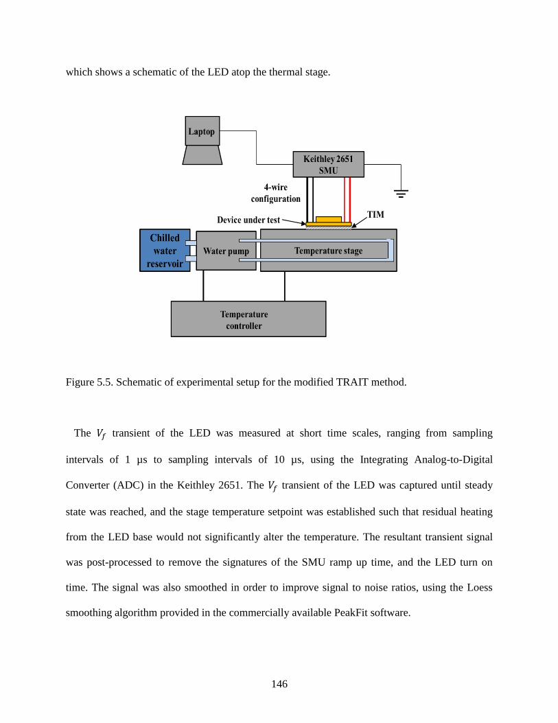
146
which shows a schematic of the LED atop the thermal stage.
Figure 5.5. Schematic of experimental setup for the modified TRAIT method.
The transient of the LED was measured at short time scales, ranging from sampling
intervals of 1 µs to sampling intervals of 10 µs, using the Integrating Analog-to-Digital
Converter (ADC) in the Keithley 2651. The transient of the LED was captured until steady
state was reached, and the stage temperature setpoint was established such that residual heating
from the LED base would not significantly alter the temperature. The resultant transient signal
was post-processed to remove the signatures of the SMU ramp up time, and the LED turn on
time. The signal was also smoothed in order to improve signal to noise ratios, using the Loess
smoothing algorithm provided in the commercially available PeakFit software.
147
Finally, the transient is converted into the temperature transient by applying Eq. 2.1. The
peeling process was then conducted using the MATLAB program, wherein the time derivative of
the temperature rise of the LED, normalized by the input power, i.e., the time derivative of the
thermal impedance, is studied to discretize contributions to the heat path. The Padé
approximation and the LM fit were conducted using MATLAB, the Foster to Cauer
transformation was conducted using the Mathematica program, and simulation of the thermal
circuit was conducted using the NI Multisim circuit simulator program.
This work explores the results of the modified TRAIT method on three different
LED/package assemblies. The three devices have been shown in Fig. 5.6 below. Fig 5.6 (a) is a
commercially available white light LED affixed to an insulated metal substrate (IMS) thermal
substrate, Fig. 5.6 (b) shows a yellow light LED, and Fig. 5.6 (c) shows a white light LED
affixed to a surface mount (SMT) power substrate. The three devices were investigated using the
modified TRAIT method, and the junction to package thermal resistance in each of them was
characterized. The junction to package thermal resistance from the modified TRAIT method
applied to the white light LED with the IMS thermal substrate is compared with the
manufacturer supplied junction to package resistance for the same device, in order to establish
the effectiveness of the modified TRAIT method at identifying the junction to package resistance
in a device configuration with a complex multilayered geometry, in an experimental setup. The
results of the modified TRAIT method applied to the yellow light LED, and the white light LED
with an SMT substrate then presented. These are devices whose manufacturer specified thermal
properties are not known.

148
(a) (b)
(c)
Figure 5.6 (a) White light LED with IMS thermal substrate (b) Yellow light LED and (c) SMT
white light LED
In the following sections, the experimental results and analysis from the modified TRAIT
method are presented. A demonstration of the modified TRAIT method on numerical data from
an ANSYS based thermal model of an LED package is discussed first. Experimental results from
device measurmeents are then presented. The device thermal resistance of the white light LED
with an IMS substrate is compared with the thermal resistance provided by the manufacturer, and
good agreement is seen. Note that the analyses presented in this chapter assume that all the input
power supplied to the devices is converted into heat. This assumption is made due to the lack of
information about the WPE of the tested LEDs, and (in the case of visible LEDs) to conform to
the convention that the LED manufacturers have used to report their junction to package thermal
resistance.
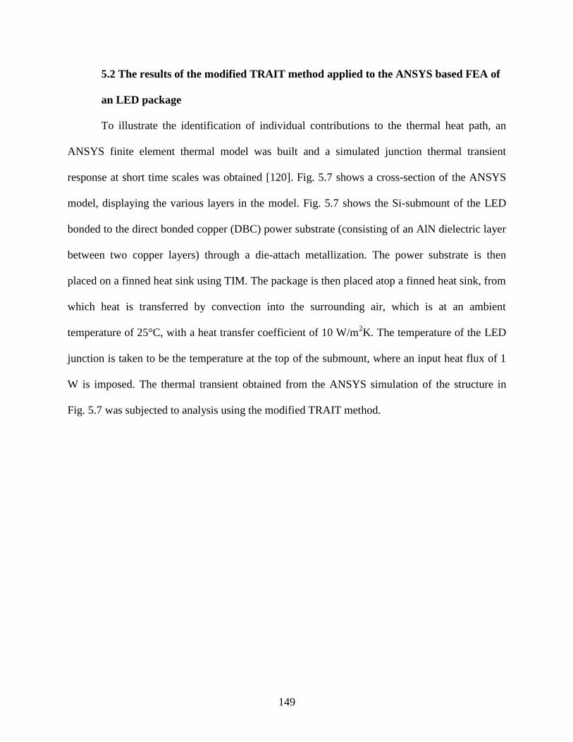
149
5.2 The results of the modified TRAIT method applied to the ANSYS based FEA of
an LED package
To illustrate the identification of individual contributions to the thermal heat path, an
ANSYS finite element thermal model was built and a simulated junction thermal transient
response at short time scales was obtained [120]. Fig. 5.7 shows a cross-section of the ANSYS
model, displaying the various layers in the model. Fig. 5.7 shows the Si-submount of the LED
bonded to the direct bonded copper (DBC) power substrate (consisting of an AlN dielectric layer
between two copper layers) through a die-attach metallization. The power substrate is then
placed on a finned heat sink using TIM. The package is then placed atop a finned heat sink, from
which heat is transferred by convection into the surrounding air, which is at an ambient
temperature of 25°C, with a heat transfer coefficient of 10 W/m2K. The temperature of the LED
junction is taken to be the temperature at the top of the submount, where an input heat flux of 1
W is imposed. The thermal transient obtained from the ANSYS simulation of the structure in
Fig. 5.7 was subjected to analysis using the modified TRAIT method.

150
Figure 5.7. Schematic of cross-section of ANSYS model used to produce the temperature
transient of the junction of a packaged LED using ANSYS based finite element analysis.
Fig. 5.8 shows the individual contributions to the 1D thermal resistance pathway from the
junction to air. Fig. 5.8 graphs the rate of change of thermal impedance of the junction, plotted
against time, on a log-log scale. Changes of slope in the rate of change point to the
discontinuities between two layers of different thermal properties. Identifying the times at which
these changes of slope occur, is analogous to identifying the times at which contributions from a
layer begin to dominate. The curve shown in Fig. 5.8 is divided into 5 stages, which correspond
to material layers with different thermal responses. The initial portion of the curve shown in Fig.
5.8 is dominated by Stage 1, which extends until 2.87x10⁻⁷
s. The thermal response of Stage 2
extends between 2.8x10⁻⁷
s to 3.6 ms, and the response of Stage 3 extends from 3.6 ms to 920 ms.
Stage 4 extends from 920 ms to 300 s, and Stage 5 extends beyond 300 s. Stage 1, 2 and 3
together correspond to the thermal response of the LED die, die attach, DBC substrate and the
TIM layer. Stage 4 and Stage 5 together correspond to the thermal response of the heat sink and
natural convection.
151
Figure 5.8. Discretization of the ANSYS generated thermal transient of the LED junction based
on the change of slope of the time rate of change of the thermal impedance of the device
junction.
The discretization of the temperature transient with respect to the spatial domains described in
Fig. 5.8 was used for the peeling procedure, after which the modified TRAIT method was
applied to the thermal transient curve. The TRAIT method yielded a five exponential fit to the
thermal resistance network from the LED junction to air. The subsequent thermal resistance
network is shown in Table 5.1 below, which outlines the thermal resistances and capacitances of
the different thermal response stages identified in Fig. 5.8. Table 5.1 shows the thermal
resistance and capacitance of Stages 1 through 5, which are the thermal resistance of the die-TIM
(Stages 1, 2 and 3) and heat sink and natural convection (Stages 4 and 5). Table 5.1 also shows
the comparison between the thermal resistance of the die-TIM, and heat sink and natural
10-10
10-5
100
105
10-10
10-5
100
105
1010
Time (s)
dZ
/dt
(K/W
s)
Stage 1
Stage 2
Stage 3
Stage 4
Stage 5

152
convection domains derived from the TRAIT method and derived from the ANSYS thermal
model.
Table 5.1. Thermal resistances and capacitances derived from the modified TRAIT method, for
the ANSYS based thermal finite element model of packaged LED.
Table 5.1 shows the thermal resistance of the die-TIM thermal pathway from the modified
TRAIT method to be 8.11 K/W, which matches the ANSYS derived thermal resistance within
13.4 %. The thermal resistance of the heat sink and convection layer is found to be 28.6 K/W
from the modified TRAIT method, which matches the ANSYS derived thermal resistance within
3.3 %. More information about calculation of the ANSYS thermal resistances presented in Table
5.1 is shown in Ha, 2009 [120]. Furthermore, Table 5.1 details the thermal resistances of Stages
1, 2, 3, 4 and 5 to be 3.50x10⁻³
K/W, 4.88 K/W, 3.23 K/W, and 23.1 K/W and 5.52 K/W,
respectively. The thermal capacitances of Stages 1, 2, 3, 4 and 5 were found to be 8.06x10⁻⁵
J/K,
5.37x10⁻⁵
J/K, 3.5x10⁻²
J/K, 7.26 J/K and 7.62 K/W respectively.
Layer Layer R (K/W) C(J/K) RTRAIT RANSYS
Percentage
Difference
Die-TIM
Stage 1 3.50x10⁻³
8.06x10⁻⁵
8.11 7.15 13.4% Stage 2 4.55 5.37x10⁻⁵
Stage 3 3.23 3.50x10⁻²
Heat sink and
natural
convection
Stage 4 23.1 7.26
28.6 29.6 3.3%
Stage 5 5.52 7.62

153
The thermal resistances and capacitances described in Table 5.1 were used to construct an
analogous five cell Cauer circuit, whose voltage transient was representative of the temperature
transient of the LED junction. This Cauer circuit is shown in Fig. 5.9 below.
Figure 5.9. The five stage Cauer circuit representation of the heat pathway out of the junction of
the LED, for the ANSYS generated thermal model of the packaged LED.
The Cauer network in Fig. 5.9 was provided with a step input power of 1 W and simulated
using a commercially available circuit simulator (NI Multisim) to obtain the voltage transient of
the electrical circuit. Fig. 5.10 below shows the temperature rise of the LED junction with time,
from the ANSYS simulation, and from the results derived by the modified TRAIT method. Fig.
5.10 shows excellent agreement between the modified TRAIT method and the ANSYS
simulation. The total junction to air thermal resistance from the ANSYS simulation as well as
that resulting from the modified TRAIT method was 36.7 K/W, with the modified TRAIT
method predicting the total thermal resistance within a percentage error of 0.013 %.
C1
8.06e-005 F
R1
0.0035004 Ω
C2
5.37e-005 F
R2
4.87972 Ω
I
0 A 1 A
100ksec 200ksec
C3
0.0350103 F
R3
3.22778 Ω
R4
23.0881 Ω
C4
7.26232 F
R5
5.52312 Ω
C5
7.6194 F

154
Figure 5.10. Temperature rise with time, for the ANSYS generated finite element thermal model,
and the results of the modified TRAIT method, at an input power of 1W.
5.3 The results of the modified TRAIT method applied to the white light LED with
an IMS substrate
The voltage transient of the white light LED with an insulated metal substrate (IMS)
thermal substrate was obtained at a step input power of 2.02 W, corresponding to an input
current of 600 mA. This voltage transient was converted to the temperature transient of the LED
junction using the and relationship described in Eq. 2.1. The method calibration curve
for the white light LED with thermal substrate was conducted at an input current of 600 mA, at
stage temperatures between 60°C and 90°C. The parameters and in Eq. 2.1, for the packaged
white light LED, were found to be -0.00358V/°C and 3.59 V respectively, and the coefficient of
determination of fit, , was determined to be 0.998. The temperature transient was then
0 2000 4000 6000 8000 100000
10
20
30
40
Time (s)
Tem
pera
ture R
ise (
K)
ANSYS Thermal Model
Modified TRAIT Method

155
discretized into its component contributions using the rate of change of impedance of the
junction, which is graphed against time, in Fig. 5.11.
As can be seen from Fig. 5.11, the thermal response of the white light LED with thermal
substrate can be attributed to two contributions; the junction-to-package resistance, and the
solder-TIM –thermal substrate resistance. Fig. 5.11 shows the thermal contribution of the
junction-to-package resistance dominates until 4.25 x10⁻⁴
s and the solder-TIM-thermal substrate
resistance dominates from 4.25 x10⁻⁴
s to 11.24 s. Based on this discretization, the modified
TRAIT method was applied to the white light LED with thermal substrate to find the thermal
parameters for the white light LED with thermal substrate. Using this, the electro-thermal
analogy for the conduction heat path from the junction of the LED, to the thermal stage, was
found. Table 5.2 shows the results of the modified TRAIT method.

156
Figure 5.11. Identification of thermal contributions, based on the time rate of change of the
thermal impedance of the junction of the white light LED with thermal substrate.
Table 5.2 shows the thermal resistance and capacitance of the junction-to-package layer to be
7.39 K/W and 8.98x10⁻³
J/K respectively. The junction-to-package thermal resistance found
through the modified TRAIT method compares well with the manufacturer specified junction-to-
package thermal resistance, which has been specified to be 8 K/W [121]. Thus, the modified
TRAIT method is able to predict the junction-to-package resistance to an accuracy of 92.4 %,
based on the experimentally measured thermal transient of the LED junction. The solder-TIM-
thermal substrate layer was found to have a thermal resistance and capacitance of 5.64 K/W and
0.184 J/K respectively. The thermal parameters shown in Table 5.2 were used to construct the
Cauer electrical circuit shown in Fig. 5.12.
10-10
10-5
100
105
10-4
10-2
100
102
104
Time (s)
dZ
/dt
(K/W
s)
TIM
Junction
-to- Package

157
Table 5.2. Thermal resistances and capacitances derived from the modified TRAIT method, for
the white light LED with an IMS substrate.
Figure 5.12. The two stage Cauer circuit representation of the heat pathway out of the junction of
the LED, for the white light LED with an IMS thermal substrate.
The Cauer circuit shown in Fig. 5.12 was simulated at a step input power of 2.02 W, to obtain
the transient thermal response of the device. The voltage response of the simulated circuit is
analogous to the temperature response of the thermal network from the device junction to the
thermal stage. Fig. 5.13 below compares the simulated temperature rise with the experimentally
measured temperature rise of the junction of the white light LED with thermal substrate. Good
agreement can be seen between the simulated and measured temperature rises. The junction to
thermal stage thermal resistance, i.e., the total conduction thermal resistance out of the LED
Layer R (K/W) C(J/K)
Junction-to-package 7.39 8.98x10⁻³
TIM 5.64 1.84x10⁻¹

158
junction, was experimentally found to be 13.3 K/W. From simulation, the junction to thermal
stage thermal resistance was found to be 13.0 K/W. Thus, the modified TRAIT method was able
to identify the total junction to thermal stage thermal resistance to an accuracy of 98.1 %.
Figure 5.13. Temperature rise with time, for the white light LED with an IMS substrate, from the
experiment and the modified TRAIT method, at an input power of 2.02 W.
5.4 The results of the modified TRAIT method applied to the white light LED with
an SMT substrate
The white light LED with the surface mount (SMT) power substrate was supplied with a
step input power of 888 mW (corresponding to an input current of 300 mA). The voltage
transient thus obtained was transformed into the temperature transient response of the LED using
0 10 20 300
5
10
15
20
25
30
Time (s)
Tem
peratu
re R
ise (
K)
Experiment
Modified TRAIT Method

159
Eq. 2.1. For the white light LED, the parameters and in Eq. 2.1 were found to be -0.00299
V/°C and 3.19672 V respectively. The was found to be 0.998. The relationship between the
and junction temperature described in Eq. 2.1 was conducted at an input current of 300 mA, at
stage temperatures between 60°C and 90°C.
Fig. 5.14 below shows the rate of change of thermal impedance for the thermal transient
obtained from the SMT white light LED. It can be seen from Fig. 5.14 that the thermal transient
of the LED can be separated into two regions. In the first region, which extends until 1 ms, is the
time regime dominated by the thermal response of the junction-to-package resistance. The
second region, extended between 1 ms until steady state us reached (in Fig. 5.14, at 12.5 s), is the
region of the thermal transient dominated by the thermal resistance of the TIM layer. On the
basis of this discretization of the thermal response, the modified TRAIT method was applied to
find the thermal parameters of the SMT white light LED.
The thermal resistance and thermal capacitance found using the modified TRAIT method for
the SMT white light LED is shown in Table 5.3 below. Table 5.3 shows the junction-to-package
thermal resistance and capacitance to be 7.76 K/W, and 9.4x10⁻³
J/K respectively. The thermal
resistance and capacitance of the TIM layer were found to be 0.858 K/W and 0.875 J/K
respectively. There thermal parameters were used to simulate the Cauer circuit, shown in Fig.
5.15 below, with an input power of 888 mW. The voltage rise across the Cauer circuit is
indicative of the temperature rise of the junction of the LED.

160
Figure 5.14.. Identification of thermal contributions, based on the time rate of change of the
thermal impedance of the junction of the white light LED with SMT power substrate.
Figure 5.15. The two stage Cauer circuit representation of the heat pathway out of the junction of
the LED, for the white light LED with SMT power substrate.
10-4
10-2
100
102
10-5
100
105
Time (s)
dZ
/dt
(K/W
s)
Junction
-to- Package
TIM
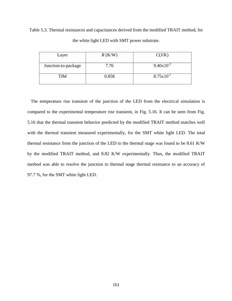
161
Table 5.3. Thermal resistances and capacitances derived from the modified TRAIT method, for
the white light LED with SMT power substrate.
Layer R (K/W) C(J/K)
Junction-to-package 7.76 9.40x10⁻³
TIM 0.858 8.75x10⁻¹
The temperature rise transient of the junction of the LED from the electrical simulation is
compared to the experimental temperature rise transient, in Fig. 5.16. It can be seen from Fig.
5.16 that the thermal transient behavior predicted by the modified TRAIT method matches well
with the thermal transient measured experimentally, for the SMT white light LED. The total
thermal resistance from the junction of the LED to the thermal stage was found to be 8.61 K/W
by the modified TRAIT method, and 8.82 K/W experimentally. Thus, the modified TRAIT
method was able to resolve the junction to thermal stage thermal resistance to an accuracy of
97.7 %, for the SMT white light LED.

162
Figure 5.16. Temperature rise with time, for the SMT white light LED, from the experiment and
the modified TRAIT method, at an input power of 0.888 W.
5.5 The results of the modified TRAIT method applied to the yellow light LED
The yellow light LED was supplied with a step input power of 0.983 mW (corresponding
to an input current of 385 mA), and the resulting voltage transient was recorded. The and
relationship was used to convert this voltage response into a temperature response, according to a
calibration. The calibration curve of the yellow light LED was conducted at an input current
of 385 mA, conducted over stage temperatures between 50°C and 80°C in intervals of 10°C. For
the yellow light LED, the parameters and in Eq. 2.1 are -0.0041 V/°C and 2.88°C. The
was determined to be 0.999. Fig. 5.17 shows the graph of the rate of change of thermal
impedance, for the yellow light LED. It can be seen from Fig. 5.17 that the thermal transient of
the yellow light LED can be separated into time domains where the thermal resistance from the
junction of the LED to the bottom of the LED package dominates, and where the resistance of
0 2 4 6 8 10 12 140
2
4
6
8
10
Time (s)
Tem
pera
ture R
ise (
K)
Experiment
Modified TRAIT Method

163
the TIM dominates. The former region extends until approximately 1.57 ms, and the latter
extending beyond 1.57 ms. The peeling process, and the consequent analysis for thermal
parameters, is executed on the basis of this separation.
The results of the modified TRAIT method indicate a two exponential fit, whose Cauer circuit
parameters, the thermal resistance and the thermal capacitance is given in Table 5.4 below. Table
5.4 also shows a description of the circuit parameters. Table 5.4 shows the junction-to-package
thermal resistance of the yellow light LED to be 10.2 K/W, and the thermal capacitance to be
1.56 x 10⁻⁴
J/K. It is also seen from Table 5.4, that the TIM thermal resistance was 2.7 K/W,
while the thermal capacitance is found to be 2.28 x 10⁻³
J/K.
Figure 5.17. Identification of thermal contributions, based on the time rate of change of the
thermal impedance of the junction of the yellow light LED.
10-6
10-4
10-2
100
100
102
104
Time (s)
dZ
/dt
(K/W
s)
TIM
Junction - to- Package
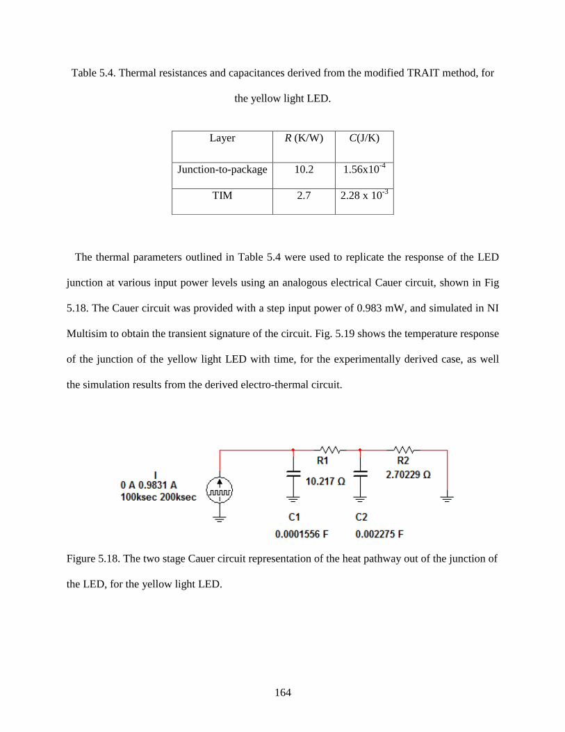
164
Table 5.4. Thermal resistances and capacitances derived from the modified TRAIT method, for
the yellow light LED.
The thermal parameters outlined in Table 5.4 were used to replicate the response of the LED
junction at various input power levels using an analogous electrical Cauer circuit, shown in Fig
5.18. The Cauer circuit was provided with a step input power of 0.983 mW, and simulated in NI
Multisim to obtain the transient signature of the circuit. Fig. 5.19 shows the temperature response
of the junction of the yellow light LED with time, for the experimentally derived case, as well
the simulation results from the derived electro-thermal circuit.
Figure 5.18. The two stage Cauer circuit representation of the heat pathway out of the junction of
the LED, for the yellow light LED.
Layer R (K/W) C(J/K)
Junction-to-package 10.2 1.56x10⁻⁴
TIM 2.7 2.28 x 10⁻³

165
Figure 5.19. Temperature rise with time, for the yellow LED, from the experiment and the
modified TRAIT method, at an input power of 0.983 W.
As can be seen from Fig. 5.19, the temperature rise of the LED junction concluded from the
modified TRAIT method matches closely with the temperature rise measured for the yellow light
LED. The total thermal resistance of the conduction pathway from the device junction, i.e., the
junction to thermal stage thermal resistance, was found to be 11.8 K/W from the experiment, and
12.9 K/W from simulation. Thus, the modified TRAIT method was able to resolve the junction
to thermal stage thermal resistance within 9.03 % error.
0 0.02 0.04 0.060
5
10
15
Time (s)
Tem
per
atu
re R
ise
(K)
Experiment
Modified TRAIT Method

166
CHAPTER 6
CONCLUSIONS AND FUTURE WORK
The motivation of this work was to investigate in a comparative manner the various ways in
which the internal temperature of an LED can be measured using electrical or optical methods,
and the merits and demerits of each method of thermometry. Temperature measurements in UV
LEDs of different device architectures and packaging schemes, measured using a variety of
thermometry techniques, were conducted.
A comparison of temperature rises measured by micro-Raman thermometry and IR
spectroscopy leads to the conclusion that while IR spectroscopy matches well with the
temperature rises of the interior layer of the micropixel devices, the same cannot be said for the
interdigitated device. While micro-Raman spectroscopy has the advantage of resolving for
vertical temperature differences within the device, it presents challenges when accurately
accounting for the inverse piezoelectric effects in some interior layers (i.e., the n- AlxGa1-xN
layer).
In comparison, while the temperature rises measured by IR spectroscopy are affected by the
surface emissivity of the device, the transmissivity of multilayers in the device, and the spatial
resolution of the IR camera in areas with large thermal gradients, IR spectroscopy measurements
are a convenient way to observe the real-time development of thermal features and temperature
distributions in the device. And, it was seen that the forward voltage method provides junction
temperature rises that cannot be reconciled with the temperature rises measured in the device
interior layers, or at the device surface. It has been determined that the forward voltage method
in UV LEDs is sensitive to the effects of Ohmic contact degradation and devices series resistance
167
on the stability of device electrical properties. Additionally, EL spectroscopy uniquely provides a
method of studying the effects of device degradation manifested in the optical emission of the
device. The use of EL spectroscopy for temperature measurements, without the use of a pulsed
input current calibration, opens new avenues for studying the temperature rise of UV LEDs using
the EL spectra in steady state operation. Temperature rise measurements using EL spectroscopy
were found to agree closely to the temperature rise of the n- AlxGa1-xN layer at the p-mesa,
measured by micro-Raman spectroscopy.
For a thorough understanding of temperature rise in an LED, the combined use of the micro-
Raman and IR spectroscopy methods is recommended. Using the two methods concurrently
allows for the detection of any possible vertical temperature differences in the device, as well as
the real time monitoring of surface temperature differences can be monitored in real-time.
Future work recommended in this area includes an in-depth examination of inverse-
piezoelectric stresses in the n- AlxGa1-xN layer in UV LEDs using numerical simulation, and
using micro-Raman spectroscopy for the simultaneous measurement of the Stokes peak position
and linewidth and comparison of peak parameters to a calibration stress. The use of confocal
Raman spectroscopy to measure more depth specific temperatures inside the device is also
recommended.
It is recommended that the EL spectroscopy method be utilized to relate device temperature
measurements to optical output characteristics at various levels of temperature and current stress.
The use of EL spectroscopy with a pulsed input current for the calibration of junction
temperature and wavelength shift, should be conducted and compared with the resulted from the
calibration of junction temperature and wavelength shift based on a continuous wave input
current calibration.
168
Another motivation of this work was to find the package thermal resistance external to the
LED. The junction to package resistance of LEDs has been identified in the total 1D conduction
heat path from the junction of the LED, to the thermal stage, using the modified TRAIT method.
In this work, the application of the modified TRAIT method to resolve the junction to package
resistance has been shown in an ANSYS generated thermal model of a packaged LED, as well
from experimentally derived thermal transients of commercially available visible and UV LEDs.
Good agreement was found between the results of the modified TRAIT method and the
experimental temperature rises, for all cases. Thermal resistances and thermal capacitances in
the thermal conduction pathway from the junction of the LED to ambient air, have been
identified as belonging to distinct spatial domains, using a Laplace transform based method that
does not warrant network identification based on convolution methods.
This investigation exhibits the use of the modified TRAIT method as a method to successfully
resolve junction-to-package resistances in a LED package, using commercially available
equipment and customizable data processing code. The experimental setup described in this
work can be used to characterize the LED optically as well as thermally, when assimilated with
optical monitoring techniques such as the use of an integrated sphere.
Additionally, there exist opportunities for the modified TRAIT method to be extended to study
thermal processes in two and three dimensions, allowing for the characterization of thermal
spreading resistances in LED packages. Future work regarding the modified TRAIT method is
recommended. A thorough understanding of the mathematical and numerical bounds that prevent
the detection of finer thermal signatures (i.e., corresponding to physically smaller device layers,
or highly conductive thermal layers) is needed. It is recommended that the sensitivity of the
presented modified TRAIT method be established, and the various factors affecting it be studied,

169
by application of the modified TRAIT method on various FEA generated test cases. Future work
may also involve improving upon the modified TRAIT method by examining more robust curve
fitting and curve smoothing algorithms.

170
APPENDIX A
CODE FOR MODIFIED TRAIT METHOD
% Initial processing of Temperature vector load('timelist_5layer.mat')%load files load('Templist_5layer.mat') Rth = T(1) -T(end) ;% Find the temperature rise A = (5000e-6).^2;%Find area of device q = (5e5)*A;%Find total heat input in W Tnew = (T-T(1))./q;% Find temperature rise in K/W Tnew = Tnew - Rth; %Prepare the vector as per as per Bagnoli et al., Part I,
1997 deriv = diff(Tnew)./diff(t); loglog(t(1:end-1),deriv)% Use changes of slope in this plot to determine the
regions to break the response into
%% find zero of function fzero(@QN_test,0); %%% lsqcurvefit, which is an inbuilt MATLAB function, with specified time
constants to TI(partofinterest1: partofinterest2) %% load TI for lsqcurvefit, from QN_test %% set options for lsqcurvefit with Levenberg-Marquardt %% OPTIONS =
optimset('Jacobian','on','MaxFunEvals',1000,'Algorithm','levenberg-
marquardt'); %% To fit, for example a 5 stage network, consider all tau's together, %% type in lsqcurvefit(@Tfun, [ 1 1 1 1 1], t(1:490),TI(1:490), [0 0 0 0 0],
[100 100 100 100 100])
function QNans = QN_test(p) load('Tlist_5layer.mat'); load('timelist_5layer.mat'); A = (0.05).^2; q = (400)*A; q = 1; Rth = (T(end) -T(1))/q ; Tnew = (T-T(1))./q; TI =-1*(Tnew - Rth); % The first temperature vector is the entire response deriv = diff(Tnew)./diff(t); % x = deriv(216:271); % Peel off to get the second response and so on y = TI(216:271); % Peel off to get the second response and so on tau1 = polyfit(x,y,1); Tnew1 = TI - tau1(2); ft = exp((1/tau1(1)).*t); x = ft(216:271); y = Tnew1(216:271); a1 = polyfit(x,y,1);
Tpart1 = a1(1).*exp((1/tau1(1)).*t);
TII = TI-Tpart1;
171
deriv = diff(TII)./diff(t) x = deriv(7:215); y = TII(7:215); tau2 = polyfit(x,y,1); Tnew2 = TII - tau2(2); ft2 = exp((1/tau2(1)).*t); x = ft2(7:215); y = Tnew2(7:215); a2 = polyfit(x,y,1);
Tpart2 = a2(1).*exp((1/tau2(1)).*t);
TIII = TII-Tpart2; deriv = diff(TIII)./diff(t) x = deriv(1:6); y = TIII(1:6); tau3 = polyfit(x,y,1); Tnew3 = TIII - tau3(2); ft3 = exp((1/tau3(1)).*t); x = ft3(1:6); y = Tnew3(1:6); a3 = polyfit(x,y,1);
Tpart3 = a3(1).*exp((1/tau3(1)).*t);
% Now we have peeled the entire response into three parts
%%% For the following lines, refer to Pade approximation from Bagnoli et al.,
Part I, 1997
N = 4; t1 = t(216:271)'; FT1 = TIII(216:271)'; difft1 = diff(t1); lambda = 0.005; NN = 2*N; t11 = t1(1,end-1); FT11 = FT1(1,end-1); elam = exp(-1*lambda.*t11); for n = 1:NN; kn = FT11*(t11.^(n)).*elam.*difft1; knsum = sum(kn); gn1(n) = ((-1.^n)./factorial(n))*knsum; end
A = zeros(N); A(1,1:end) = gn1(5:-1:2); A(2,1:end) = gn1(6:-1:3); A(3,1:end) = gn1(7:-1:4); A(4,1:end) = gn1(8:-1:5); gn11=gn1'; B = gn11(1:4); C = A\B; D = [gn11(1),0,0,0;
172
gn11(2),gn11(1),0,0; gn11(3),gn11(2),gn11(1),0; gn11(4),gn11(3),gn11(2),gn11(1)]; E = D*C;
QNans= C(1,1) + (C(2,1).*p)+(C(3,1).*(p.^2))+(C(4,1).*(p.^3))+(p.^4);
% Function for fitting to entire response, example given for 4 part response function out = Tfun(x,tau, t)%tau and x are to be found Tpart1 = x(1)*exp((-1/tau(1)).*t) Tpart2 = x(2)*exp((-1/tau(2)).*t) Tpart3 = x(3)*exp((-1/tau(3)).*t) Tpart4 = x(4)*exp((-1/tau(4)).*t) out= (Tpart1 + Tpart2 + Tpart3+Tpart4)% summing up responses according to
exponential
end
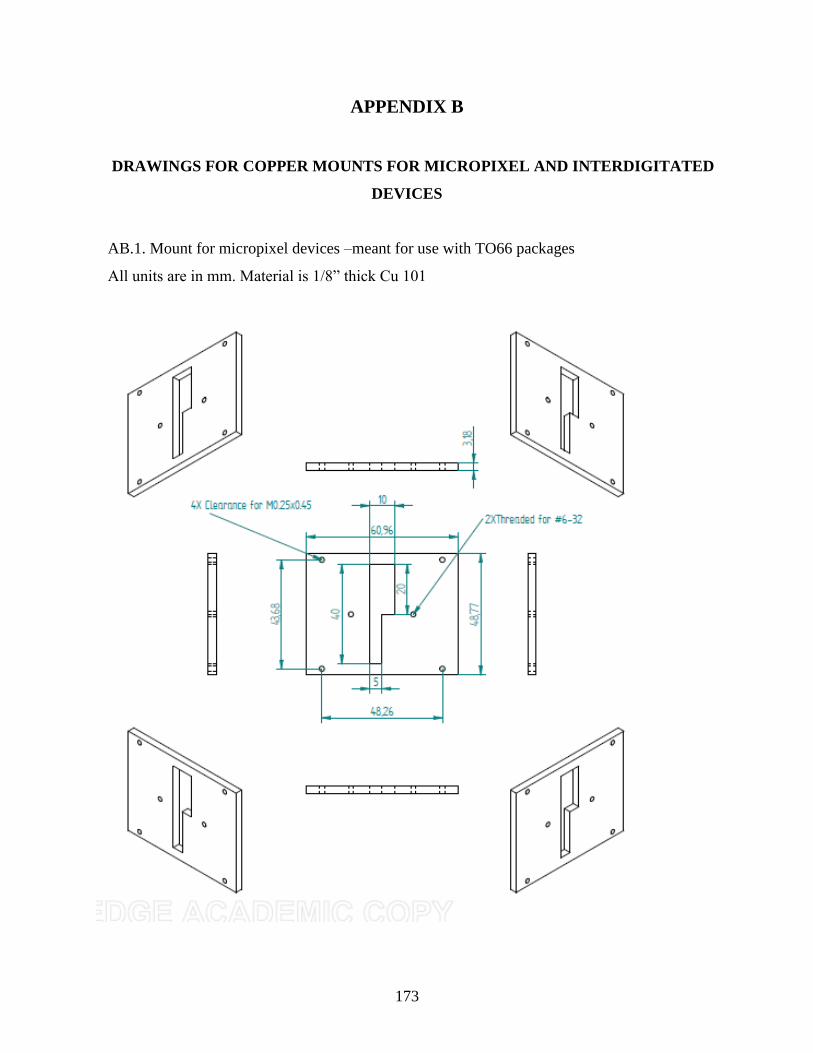
173
APPENDIX B
DRAWINGS FOR COPPER MOUNTS FOR MICROPIXEL AND INTERDIGITATED
DEVICES
AB.1. Mount for micropixel devices –meant for use with TO66 packages
All units are in mm. Material is 1/8” thick Cu 101

174
AB.2. Mount for micropixel devices –meant for use with TO3 packages
All units are in inches. Material is 1/4” thick Cu 101

175
AB.3. Mount for interdigitated devices

176
APPENDIX C
DRAWINGS FOR COPPER MOUNT TO FIX HOT PLATE ONTO RAMAN
MICROSCOPE STAGE
1/8” thick Al. All units are in mm unless specified.

177
REFERENCES
[1] A. Bergh, G. Craford, A. Duggal, and R. Haitz, "The Promise and Challenge of Solid-
State Lighting," Physics Today, vol. 54, p. 42, 2001.
[2] F. A. Ponce and D. P. Bour, "Nitride-based semiconductors for blue and green light-
emitting devices," Nature, vol. 386, pp. 351-359, 1997.
[3] M. R. Krames, O. B. Shchekin, R. Mueller-Mach, G. O. Mueller, Z. Ling, G. Harbers,
and M. G. Craford, "Status and Future of High-Power Light-Emitting Diodes for Solid-
State Lighting," Journal of Display Technology, vol. 3, pp. 160-175, 2007.
[4] E. F. Schubert, "History of Light Emitting Diodes " in Light-Emitting Diodes 2nd ed New
York, USA: Cambridge University Press 2006, pp. 1-22.
[5] E. F. Schubert, "Communication LEDs," in Light-Emitting Diodes ed New York, USA:
Cambridge University Press 2006, pp. 382-388.
[6] T. N. Oder, K. H. Kim, J. Y. Lin, and H. X. Jiang, "III-nitride blue and ultraviolet
photonic crystal light emitting diodes," Applied Physics Letters, vol. 84, p. 466, 2004.
[7] Y. Taniyasu, M. Kasu, and T. Makimoto, "An aluminium nitride light-emitting diode
with a wavelength of 210 nanometres," Nature, vol. 441, pp. 325-328, 2006.
[8] NASA. (January 26th 2012). A diagram of the EM spectrum. Available:
http://upload.wikimedia.org/wikipedia/commons/c/cf/EM_Spectrum_Properties_edit.svg
[9] A. Khan, K. Balakrishnan, and T. Katona, "Ultraviolet light-emitting diodes based on
group three nitrides," Nature Photonics, vol. 2, pp. 77-84, 2008.
[10] A. Khan and K. Balakrishnan, "Present Status of Deep UV Nitride Light Emitters,"
Materials Science Forum, vol. 590, pp. 141-174, 2008.
[11] M. A. Würtele, T. Kolbe, M. Lipsz, A. Külberg, M. Weyers, M. Kneissl, and M. Jekel,
"Application of GaN-based ultraviolet-C light emitting diodes – UV LEDs – for water
disinfection," Water Research, vol. 45, pp. 1481-1489, 2011.
[12] A. C. Chevremont, A. M. Farnet, M. Sergent, B. Coulomb, and J. L. Boudenne,
"Multivariate optimization of fecal bioindicator inactivation by coupling UV-A and UV-
C LEDs," Desalination, vol. 285, pp. 219-225, 2012.
[13] A. Zukauskas, N. Kurilcik, P. Vitta, S. Jursenas, E. Bakiene, and R. Gaska, "Optimization
of a UV light-emitting diode based fluorescence-phase sensor," in Optically Based
Biological and Chemical Detection for Defence III. vol. 6398, J. C. Carrano and A.
Zukauskas, Eds., ed Bellingham: Spie-Int Soc Optical Engineering, 2006.

178
[14] D. M. Reilly, D. T. Moriarty, and J. A. Maynard, "Unique properties of solar blind
ultraviolet communication systems for unattended ground sensor networks,"
Unmanned/Unattended Sensors and Sensor Networks, vol. 5611, pp. 244-254, 2004.
[15] G. A. Shaw, A. M. Siegel, J. Model, and D. Greisokh, "Recent progress in short-range
ultraviolet communication," in SPIE, 2005, pp. 214-225.
[16] M. Kneissl, T. Kolbe, C. Chua, V. Kueller, N. Lobo, J. Stellmach, A. Knauer, H.
Rodriguez, S. Einfeldt, Z. Yang, N. M. Johnson, and M. Weyers, "Advances in group III-
nitride-based deep UV light-emitting diode technology," Semiconductor Science and
Technology, vol. 26, p. 014036, 2011.
[17] E. F. Schubert, "LED Basics : Optical Properties " in Light-Emitting Diodes 2nd ed New
York, USA: Cambridge University Press 2006, pp. 86-91.
[18] E. F. Schubert, "LED Basics: Electrical Properties " in Light-Emitting Diodes. vol. 59-85,
2nd ed Cambridge, UK: Cambridge University Press, 2010, pp. 59-84.
[19] E. F. Schubert. (2004, Octber 10, 2012). Light Emitting Diodes [Online multimedia ].
Available: http://www.ecse.rpi.edu/~schubert/Light-Emitting-Diodes-dot-
org/chap04/F04-01%20PN%20junction%20energies.jpg
[20] E. F. Schubert, "Chapter 4: LED basics: Electrical properties, Fig.4.12.(a)," ed, 2004.
[21] A. Isamu, "Progress in crystal growth of nitride semiconductors," Journal of Crystal
Growth, vol. 221, pp. 231-239, 2000.
[22] E. F. Schubert, in Light-Emitting Diodes 2nd ed Cambridge, United Kingdom:
Cambridge University Press, 2010, pp. 222-234.
[23] Y. Taniyasu and M. Kasu. (2010, October 6, 2012). Improved Emmision Efficiency of
210 nm Deep-ultraviolet Aluminum Nitride Light-emitting Diode NTT Technical Review
[Technical article]. 8(8). Available: https://www.ntt-
review.jp/archive/ntttechnical.php?contents=ntr201008sf2.pdf&mode=show_pdf
[24] G. Tech-CNRS. (October 6). Growth on unconventional substrates. Available:
http://www.umi2958.eu/spip.php?rubrique75
[25] E. F. Schubert, "High internal efficieny designs," in Light-Emitting Diodes, ed
Cambridge, UK: University Press, 2010, pp. 113-126.
[26] E. F. Schubert, "Chapter 7: High internal efficiency LED designs, Fig. 7.12," 2nd
ed,
2004.
[27] E. F. Schubert, "Chapter 7: High internal efficiency LED designs, Fig. 7.14," 2nd
ed,
2004.

179
[28] M. Imura, K. Nakano, N. Fujimoto, N. Okada, K. Balakrishnan, M. Iwaya, S. Kamiyama,
H. Amano, I. Akasaki, T. Noro, T. Takagi, and A. Bandoh, "Dislocations in AIN
epilayers grown on sapphire substrate by high-temperature metal-organic vapor phase
epitaxy," Japanese Journal of Applied Physics Part 1-Regular Papers Brief
Communications & Review Papers, vol. 46, pp. 1458-1462, Apr 2007.
[29] J. W. Matthews and A. E. Blakeslee, "Defects in epitaxial multilayers: III. Preparation of
almost perfect multilayers," Journal of Crystal Growth, vol. 32, pp. 265-273, 1976.
[30] E. F. Schubert, "Dislocations in III-V nitrides " in Light-Emitting Diodes ed Cambridge,
UK: University Press, 2010, pp. 227-231.
[31] J. P. Zhang, M. A. Khan, W. H. Sun, H. M. Wang, C. Q. Chen, Q. Fareed, E. Kuokstis,
and J. W. Yang, "Pulsed atomic-layer epitaxy of ultrahigh-quality AlxGa1-xN structures
for deep ultraviolet emissions below 230 nm," Applied Physics Letters, vol. 81, pp. 4392-
4394, Dec 2002.
[32] J. R. Grandusky, J. A. Smart, M. C. Mendrick, L. J. Schowalter, K. X. Chen, and E. F.
Schubert, "Pseudomorphic growth of thick n-type AlxGa1−xN layers on low-defect-
density bulk AlN substrates for UV LED applications," Journal of Crystal Growth, vol.
311, pp. 2864-2866, 2009.
[33] E. F. Schubert, "UV devices emitting at wavelengths shorter than 360 nm," in Light-
Emitting Diodes, 2nd ed Cambridge, UK: Cambridge University Press 2010, pp. 233-235.
[34] J. P. Zhang, H. M. Wang, M. E. Gaevski, C. Q. Chen, Q. Fareed, J. W. Yang, G. Simin,
and M. A. Khan, "Crack-free thick AlGaN grown on sapphire using AlN/AlGaN
superlattices for strain management," Applied Physics Letters, vol. 80, pp. 3542-3544,
May 2002.
[35] H. Hirayama, S. Fujikawa, N. Noguchi, J. Norimatsu, T. Takano, K. Tsubaki, and N.
Kamata, "222–282 nm AlGaN and InAlGaN-based deep-UV LEDs fabricated on high-
quality AlN on sapphire," physica status solidi (a), vol. 206, pp. 1176-1182, 2009.
[36] C. Pernot, M. Kim, S. Fukahori, T. Inazu, T. Fujita, Y. Nagasawa, A. Hirano, M.
Ippommatsu, M. Iwaya, S. Kamiyama, I. Akasaki, and H. Amano, "Improved Efficiency
of 255-280 nm AlGaN-Based Light-Emitting Diodes," Applied Physics Express, vol. 3,
2010.
[37] X. Guo and E. F. Schubert, "Current crowding in GaN/InGaN light emitting diodes on
insulating substrates," Journal of Applied Physics, vol. 90, pp. 4191-4195, 2001.
[38] H. Kim, S.-J. Park, H. Hwang, and N.-M. Park, "Lateral current transport path, a model
for GaN-based light-emitting diodes: Applications to practical device designs," Applied
Physics Letters, vol. 81, p. 1326, 2002.
180
[39] V. Adivarahan, A. Heidari, B. Zhang, Q. Fareed, S. Hwang, M. Islam, and A. Khan, "280
nm Deep Ultraviolet Light Emitting Diode Lamp with an AlGaN Multiple Quantum Well
Active Region," Applied Physics Express, vol. 2, p. 102101, 2009.
[40] V. Adivarahan, S. Wu, W. H. Sun, V. Mandavilli, M. S. Shatalov, G. Simin, J. W. Yang,
H. P. Maruska, and M. A. Khan, "High-power deep ultraviolet light-emitting diodes
based on a micro-pixel design," Applied Physics Letters, vol. 85, pp. 1838-1840, 2004.
[41] J. J. Wierer, D. A. Steigerwald, M. R. Krames, J. J. O'Shea, M. J. Ludowise, G.
Christenson, Y. C. Shen, C. Lowery, P. S. Martin, S. Subramanya, W. Gotz, N. F.
Gardner, R. S. Kern, and S. A. Stockman, "High-power AlGaInN flip-chip light-emitting
diodes," Applied Physics Letters, vol. 78, pp. 3379-3381, May 2001.
[42] D. A. Steigerwald, J. C. Bhat, D. Collins, R. M. Fletcher, M. O. Holcomb, M. J.
Ludowise, P. S. Martin, and S. L. Rudaz, "Illumination with solid state lighting
technology," IEEE Journal of Selected Topics in Quantum Electronics, vol. 8, pp. 310-
320, 2002.
[43] B. Christie. (2002), [Illustration ]. Available:
http://spectrum.ieee.org/semiconductors/optoelectronics/let-there-be-light
[44] A. Chitnis, J. Sun, V. Mandavilli, R. Pachipulusu, S. Wu, M. Gaevski, V. Adivarahan, J.
P. Zhang, M. A. Khan, A. Sarua, and M. Kuball, "Self-heating effects at high pump
currents in deep ultraviolet light-emitting diodes at 324 nm," Applied Physics Letters, vol.
81, p. 3491, 2002.
[45] J. Grandusky, Y. Cui, S. Gibb, M. Mendrick, and L. Schowalter, "Performance and
reliability of ultraviolet-C pseudomorphic light emitting diodes on bulk AlN substrates,"
physica status solidi (c), vol. 7, pp. 2199-2201, 2010.
[46] M. Shatalov, "Reliability of AlGaN-based deep UV LEDs on sapphire," vol. 6134, pp.
61340P-61340P-11, 2006.
[47] X. A. Cao, S. F. LeBoeuf, and T. E. Stecher, "Temperature-dependent
electroluminescence of AlGaN-based UV LEDs," IEEE Electron Device Letters, vol. 27,
pp. 329-331, 2006.
[48] M. Meneghini, A. Tazzoli, G. Mura, G. Meneghesso, and E. Zanoni, "A Review on the
Physical Mechanisms That Limit the Reliability of GaN-Based LEDs," IEEE
Transactions on Electron Devices, vol. 57, pp. 108-118, 2010.
[49] M. Meneghini, L. Trevisanello, U. Zehnder, G. Meneghesso, and E. Zanoni, "Thermal
degradation of InGaN/GaN LEDs ohmic contacts," physica status solidi (c), vol. 5, pp.
2250-2253, 2008.

181
[50] M. Meneghini, L. Trevisanello, S. Podda, S. Buso, G. Spiazzi, G. Meneghesso, and E.
Zanoni, "Stability and performance evaluation of high brightness light emitting diodes
under DC and pulsed bias conditions - art. no. 63370R," in Sixth International
Conference on Solid State Lighting. vol. 6337, I. T. Ferguson, N. Narendran, T. Taguchi,
and I. E. Ashdown, Eds. Bellingham: Spie-Int Soc Optical Engineering, 2006, pp. R3370-
R3370.
[51] E. F. Schubert, "Packaging," in Light-Emitting Diodes, 2nd ed Cambridge, UK:
University Press, 2010, pp. 191-199.
[52] A. Christensen and S. Graham, "Thermal effects in packaging high power light emitting
diode arrays," Applied Thermal Engineering, vol. 29, pp. 364-371, 2009.
[53] Y. Habtemichael, "Packaging Designs for Ultraviolet Light Emitting Diodes," M.S.,
Mechanical Engineering, Georgia Institute of Technology, Atlanta, GA, 2012.
[54] (2008, October 6th, 2012). Seoul launches single LED package delivering 900lm at 10W
Available: http://www.semiconductor-
today.com/news_items/2008/FEB/SEOUL_290208.htm
[55] E. F. Schubert, "Chapter 11: Packaging, Fig. 11.2," ed, 2004.
[56] M. Inc. TO66 [Online Multimedia ]. Available:
http://www.microsemi.com/en/products/package-outlines/66
[57] M. Inc. TO3 [Online Multimedia]. Available:
http://www.microsemi.com/en/products/package-outlines/3
[58] Y. Xi, T. Gessmann, J. Xi, J. K. Kim, J. M. Shah, E. F. Schubert, A. J. Fischer, M. H.
Crawford, K. H. A. Bogart, and A. A. Allerman, "Junction Temperature in Ultraviolet
Light-Emitting Diodes," Japanese Journal of Applied Physics, vol. 44, pp. 7260-7266,
2005.
[59] J. Hu, L. Yang, W. J. Hwang, and M. W. Shin, "Thermal and mechanical analysis of
delamination in GaN-based light-emitting diode packages," Journal of Crystal Growth,
vol. 288, pp. 157-161, 2006.
[60] E. F. Schubert, "Diode voltage," in Light-Emitting Diodes 2nd ed Cambridge, UK:
University Press, 2010, pp. 83-84.
[61] E. F. Schubert, "Theory of temperature depedance of diode forward voltage " in Light-
Emitting Diodes, 2nd ed Cambridge, UJ: University Press, 2010, pp. 104-107.
[62] N. Bochkareva, A. Efremov, Y. Rebane, R. Gorbunov, A. Klochkov, and Y. Shreter,
"Nonuniformity of carrier injection and the degradation of blue LEDs," Semiconductors,
vol. 40, pp. 118-123, 2006.

182
[63] O. Pursiainen, N. Linder, A. Jaeger, R. Oberschmid, and K. Streubel, "Identification of
aging mechanisms in the optical and electrical characteristics of light-emitting diodes,"
Applied Physics Letters, vol. 79, pp. 2895-2897, Oct 2001.
[64] E. F. Schubert, "Carrier overflow in double heterostructures " in Light-Emitting Diodes,
2nd ed Cambridge, UK: University Press, 2010, pp. 78-81.
[65] L. X. Zhao, E. J. Thrush, C. J. Humphreys, and W. A. Phillips, "Degradation of GaN-
based quantum well light-emitting diodes," Journal of Applied Physics, vol. 103, Jan
2008.
[66] Y. Xi and E. F. Schubert, "Junction–temperature measurement in GaN ultraviolet light-
emitting diodes using diode forward voltage method," Applied Physics Letters, vol. 85, p.
2163, 2004.
[67] Y. Xi, J. Q. Xi, T. Gessmann, J. M. Shah, J. K. Kim, E. F. Schubert, A. J. Fischer, M. H.
Crawford, K. H. A. Bogart, and A. A. Allerman, "Junction and carrier temperature
measurements in deep-ultraviolet light-emitting diodes using three different methods,"
Applied Physics Letters, vol. 86, p. 031907, 2005.
[68] Y. Deng, Y. Kong, Y. Zheng, C. Zhou, D. Xi, P. Chen, S. Gu, B. Shen, R. Zhang, P. Han,
R. Jiang, and Y. Shi, "Study on strain and piezoelectric polarization of AlN thin films
grown on Si," Journal of Vacuum Science & Technology A: Vacuum, Surfaces, and
Films, vol. 23, p. 628, 2005.
[69] A. Pinos, S. Marcinkevi ius, J. ang, . Bilenko, M. Shatalov, R. Gaska, and M. S. Shur,
"Aging of AlGaN quantum well light emitting diode studied by scanning near-field
optical spectroscopy," Applied Physics Letters, vol. 95, p. 181914, 2009.
[70] A. Pinos, S. Marcinkevi ius, J. ang, R. Gaska, M. Shatalov, and M. S. Shur, Optical
studies of degradation of AlGaN quantum well based deep ultraviolet light emitting
diodes," Journal of Applied Physics, vol. 108, p. 093113, 2010.
[71] S. Chhajed, Y. Xi, T. Gessmann, J. Q. Xi, J. M. Shah, J. K. Kim, and E. F. Schubert,
"Junction temperature in light-emitting diodes assessed by different methods," in Light-
Emitting Diodes: Research, Manufacturing, and Applications IX. vol. 5739, S. A.
Stockman, H. W. Yao, and E. F. Schubert, Eds., ed, 2005, pp. 16-24.
[72] L. A. Nafie, "Theory of Raman Scattering," in Handbook of Raman Spectroscopy, I. R.
Lewis and H. G. M. Edwards, Eds., 1st ed New York, NY: Marcel Dekker, Inc. , 2001,
pp. 1-7.
[73] G. Lucazeau, "Effect of pressure and temperature on Raman spectra of solids:
anharmonicity," Journal of Raman Spectroscopy, vol. 34, pp. 478-496, 2003.

183
[74] T. Beechem, S. Graham, S. P. Kearney, L. M. Phinney, and J. R. Serrano, "Invited
Article: Simultaneous mapping of temperature and stress in microdevices using micro-
Raman spectroscopy," Review of Scientific Instruments, vol. 78, p. 061301, Jun 2007.
[75] T. E. Beechem and J. R. Serrano, "Raman Thermometry of Microdevices: Choosing a
Method to Minimize Error," Spectroscopy, vol. 26, pp. 36-44, Nov 2011.
[76] T. Hart, R. Aggarwal, and B. Lax, "Temperature Dependence of Raman Scattering in
Silicon," Physical Review B, vol. 1, pp. 638-642, 1970.
[77] M. Kuball, G. J. Riedel, J. W. Pomeroy, A. Sarua, M. J. Uren, T. Martin, K. P. Hilton, J.
O. Maclean, and D. J. Wallis, "Time-resolved temperature measurement of AlGaN/GaN
electronic devices using micro-Raman spectroscopy," IEEE Electron Device Letters, vol.
28, pp. 86-89, Feb 2007.
[78] M. Kuball, J. W. Pomeroy, S. Rajasingam, A. Sarua, M. J. Uren, T. Martin, A. Lell, and
V. Härle, "High spatial resolution micro-Raman temperature measurements of nitride
devices (FETs and light emitters)," physica status solidi (a), vol. 202, pp. 824-831, 2005.
[79] M. Kuball, S. Rajasingam, A. Sarua, M. J. Uren, T. Martin, R. S. Balmer, and K. P.
Hilton, "Self-Heating Effects in Multi-Finger AlGaN/GaN HFETs," MRS Online
Proceedings Library, vol. 743, pp. null-null, 2002.
[80] S. P. Kearney, L. M. Phinney, and M. S. Baker, "Spatially resolved temperature mapping
of electrothermal actuators by surface Raman scattering," Journal of
Microelectromechanical Systems, vol. 15, pp. 314-321, Apr 2006.
[81] M. R. Abel, S. Graham, J. R. Serrano, S. P. Kearney, and L. M. Phinney, "Raman
Thermometry of Polysilicon Microelectro- mechanical Systems in the Presence of an
Evolving Stress," Journal of Heat Transfer, vol. 129, p. 329, 2007.
[82] J. R. Serrano, L. M. Phinney, and S. P. Kearney, "Micro-Raman thermometry of thermal
flexure actuators," Journal of Micromechanics and Microengineering, vol. 16, pp. 1128-
1134, 2006.
[83] A. Sarua, M. Kuball, M. J. Uren, A. Chitnis, J. P. Zhang, V. Adivarahan, M. Shatalov,
and M. Asif Khan, "Micro-Raman Spectroscopy: Self-Heating Effects In Deep UV Light
Emitting Diodes," MRS Online Proceedings Library, vol. 743, 2002.
[84] Y. Wang, H. Xu, S. Alur, Y. Sharma, A.-J. Cheng, K. Kang, R. Josefsberg, M. Park, S.
Sakhawat, A. N. Guha, O. Akpa, S. Akavaram, and K. Das, "In Situ Temperature
Measurement of GaN-Based Ultraviolet Light-Emitting Diodes by Micro-Raman
Spectroscopy," Journal of Electronic Materials, vol. 39, pp. 2448-2451, 2010.
[85] M. Farzaneh, K. Maize, D. Lüerßen, J. A. Summers, P. M. Mayer, P. E. Raad, K. P. Pipe,
A. Shakouri, R. J. Ram, and A. H. Janice, "CCD-based thermoreflectance microscopy:

184
principles and applications," Journal of Physics D: Applied Physics, vol. 42, p. 143001,
2009.
[86] J. Christofferson and A. Shakouri, "Thermoreflectance based thermal microscope,"
Review of Scientific Instruments, vol. 76, p. 024903, 2005.
[87] D. Kendig, K. Yazawa, and A. Shakouri, "Thermal Imaging of Encapsulated LEDs," in
27th Annual IEEE Semiconductor Thermal Measurement and Management Symposium,
ed, 2011, pp. 310-313.
[88] G. Farkas, S. Haque, F. Wall, P. S. Martin, A. Poppe, Q. van Voorst Vader, and G.
Bognar, "Electric and thermal transient effects in high power optical devices," in
Twentieth Annual IEEE Semiconductor Thermal Measurement and Management
Symposium, 2004, pp. 168-176.
[89] M. Rencz, "New possibilities in the thermal evaluation, offered by transient testing,"
Microelectronics Journal, vol. 34, pp. 171-177, 2003.
[90] V. Székely, "A new evaluation method of thermal transient measurement results,"
Microelectronics Journal, vol. 28, pp. 277-292, 1997.
[91] V. Székely and T. Van Bien, "Fine structure of heat flow path in semiconductor devices:
A measurement and identification method," Solid-State Electronics, vol. 31, pp. 1363-
1368, 1988.
[92] G. C. Albright, J. A. Stump, J. D. McDonald, and H. Kaplan, ""True" temperature
measurements on microscopic semiconductor targets," in Thermosense XXI. vol. 3700, D.
H. LeMieux and J. R. Snell, Eds., ed, 1999, pp. 245-250.
[93] J. Kolzer, E. Oesterschulze, and G. Deboy, "Thermal imaging and measurement
techniques for electronic materials and devices," Microelectronic Engineering, vol. 31,
pp. 251-270, Feb 1996.
[94] P. W. Webb, "Thermal Imaging of Electronic Devices With Low Surface Emissivity "
IEEE Proceedings-G Circuits Devices and Systems, vol. 138, pp. 390-400, Jun 1991.
[95] M. F. Modest, Radiative Heat Transfer, 2nd ed. ed. USA: Elsevier Science, 2003.
[96] G. W. Lee, S. Jeon, S. N. Park, Y. S. Yoo, and C. W. Park, "Temperature and Thickness
Dependence of IR Optical Properties of Sapphire at Moderate Temperature,"
International Journal of Thermophysics, vol. 32, pp. 1448-1456, Aug 2011.
[97] E. D. Palik, Handbook of Optical Constants of Solids 1st ed. ed. USA: Academic Press,
1997.

185
[98] V. Adivarahan, Q. Fareed, S. Srivastava, T. Katona, M. Gaevski, and A. Khan, "Robust
285 nm Deep UV Light Emitting Diodes over Metal Organic Hydride Vapor Phase
Epitaxially Grown AlN/Sapphire Templates," Japanese Journal of Applied Physics, vol.
46, pp. L537-L539, 2007.
[99] S. Hwang, M. Islam, B. Zhang, M. Lachab, J. Dion, A. Heidari, H. Nazir, V. Adivarahan,
and A. Khan, "A Hybrid Micro-Pixel Based Deep Ultraviolet Light-Emitting Diode
Lamp," Applied Physics Express, vol. 4, p. 012102, 2011.
[100] J. R. Grandusky, S. R. Gibb, M. C. Mendrick, and L. J. Schowalter, "Properties of Mid-
Ultraviolet Light Emitting Diodes Fabricated from Pseudomorphic Layers on Bulk
Aluminum Nitride Substrates," Applied Physics Express, vol. 3, p. 072103, 2010.
[101] J. R. Grandusky, S. R. Gibb, M. C. Mendrick, C. Moe, M. Wraback, and L. J.
Schowalter, "High Output Power from 260nm Pseudomorphic Ultraviolet Light-Emitting
Diodes with Improved Thermal Performance," Applied Physics Express, vol. 4, Aug
2011.
[102] P. Parayanthal and F. H. Pollak, "Raman scattering in alloy semiconductors - spatial
correlation model," Physical Review Letters, vol. 52, pp. 1822-1825, 1984.
[103] M. Holtz, T. Prokofyeva, M. Seon, K. Copeland, J. Vanbuskirk, S. Williams, S. A.
Nikishin, V. Tretyakov, and H. Temkin, "Composition dependence of the optical phonon
energies in hexagonal AlxGa1−xN, Journal of Applied Physics, vol. 89, p. 7977, 2001.
[104] L. Bergman, D. Alexson, P. L. Murphy, R. J. Nemanich, M. Dutta, M. A. Stroscio, C.
Balkas, H. Shin, and R. F. Davis, "Raman analysis of phonon lifetimes in AlN and GaN
of wurtzite structure," Physical Review B, vol. 59, pp. 12977-12982, May 1999.
[105] S. Hwang, "HIGH POWER ALGAN BASED DEEP UV LED LAMPS: DESIGN,
FABRICATION AND CHARACTERIZATION," Ph.D, Electrical Engineering,
University of South Carolina Columbia, S.C., 2010.
[106] J. P. Zhang, S. Wu, S. Rai, V. Mandavilli, V. Adivarahan, A. Chitnis, M. Shatalov, and
M. A. Khan, "AlGaN multiple-quantum-well-based, deep ultraviolet light-emitting
diodes with significantly reduced long-wave emission," Applied Physics Letters, vol. 83,
p. 3456, 2003.
[107] A. J. Fischer, "Device performance of AlGaN-based 240-300-nm deep UV LEDs," vol.
5530, pp. 38-47, 2004.
[108] A. Piccirillo, G. Oliveti, M. Ciampa, and P. E. Bagnoli, "Complete characterisation of
laser diode thermal circuit by voltage transient measurements," Electronics Letters, vol.
29, pp. 318-320, 1993.

186
[109] P. E. Bagnoli, C. Casarosa, M. Ciampi, and E. Dallago, "Thermal resistance analysis by
induced transient (TRAIT) method for power electronic devices thermal characterization.
I. Fundamentals and theory," IEEE Transactions on Power Electronics, vol. 13, pp.
1208-1219, 1998.
[110] P. E. Bagnoli, C. Casarosa, E. Dallago, and M. Nardoni, "Thermal resistance analysis by
induced transient (TRAIT) method for power electronic devices thermal characterization.
II. Practice and experiments," IEEE Transactions on Power Electronics, vol. 13, pp.
1220-1228, 1998.
[111] G. Oliveti, A. Piccirillo, and P. E. Bagnoli, "Analysis of laser diode thermal properties
with spatial resolution by means of the TRAIT method," Microelectronics Journal, vol.
28, pp. 293-300, 1997.
[112] F. P. Incropera, D. P. Dewitt, T. L. Bergman, and A. S. Levine, Fundamentals of Heat
and Mass Transfer, 6 ed. Hoboken, NJ: John Wiley and Sons, 2006.
[113] H. S. Carlslaw and J. C. Jaeger, Conduction of Heat in Solids. London, UK: Oxford
University Press, 1959.
[114] F. N. Masana, "A straightforward analytical method for extraction of semiconductor
device transient thermal parameters," Microelectronics Reliability, vol. 47, pp. 2122-
2128, 2007.
[115] R. J. Blomer, "Decomposition of Compartment Transition Functions by means of the
Pade-approximation," Mathematical Biosciences, vol. 19, pp. 163-173, 1974.
[116] H. D. V. Liew, "Semilogarithmic Plots of Data Which Reflect a Continuum of
Exponential Processes," Science, vol. 138, pp. 682-683, 1962.
[117] D. W. Marquardt, "An Algorithm for Least-Squares Estimation of Nonlinear
Parameters," Journal of the Society for Industrial and Applied Mathematics, vol. 11, pp.
431-441, 1963.
[118] R. B. Hayes, E. H. Haskell, and G. H. Kenner, "An Assessment of the Levenberg-
Marquardt Fitting Algorithm on Saturating Exponential Data Sets," Ancient TL, vol. 16,
pp. 57-62, 1998.
[119] Y. C. Gerstenmaier, W. Kiffe, and G. Wachutka, "Combination of thermal subsystems by
use of rapid circuit transformation and extended two-port theory," Microelectronics
Journal, vol. 40, pp. 26-34, 2009.
[120] M. Ha, "Thermal Analysis of High Power LED Arrays," M.S. Thesis, School of
Mechanical Engineering, Georgia Institute of Technology, Atlanta, GA, 2009.

187
[121] CREE. (2011, February 29, 2012). Cree® XLamp® XR-E LED Product Family Data
Sheet [Web document ]. Available: http://www.cree.com/products/pdf/xlamp7090xr-
e.pdf


![spiral.imperial.ac.uk · Web viewGroup III nitride semiconductors are widely used in blue, green and ultraviolet light-emitting diodes (LEDs) and laser diodes (LDs) [1], and are of](https://img.pdfslide.net/doc/110x75/5e299246afcc4663a437e727/web-view-group-iii-nitride-semiconductors-are-widely-used-in-blue-green-and-ultraviolet.jpg)