Embed Size (px)
Citation preview

THERMAL SIMULATION OF MULTIPLE CHIPS LED MODULE USING
COMPUTATIONAL FLUID DYNAMIC SOFTWARE
WONG YAU YUN
A project report submitted in partial fulfilment of the
requirements for the award of the degree of
Bachelor of Engineering (Hons) Electronic Engineering
Faculty of Engineering and Green Technology
Universiti Tunku Abdul Rahman
May 2016

ii
DECLARATION
I hereby declare that this project report is based on my original work except for
citations and quotations which have been duly acknowledged. I also declare that it
has not been previously and concurrently submitted for any other degree or award at
UTAR or other institutions.
Signature : _________________________
Name : _________________________
ID No. : _________________________
Date : _________________________

III
APPROVAL FOR SUBMISSION
I certify that this project report entitled “THERMAL SIMULATION OF
MULTIPLE CHIPS LED MODULE USING COMPUTATIONAL FLUID
DYNAMIC SOFTWARE ” was prepared by WONG YAU YUN has met the
required standard for submission in partial fulfilment of the requirements for the
award of Bachelor of Engineering (Hons) Electronic Engineering at Universiti Tunku
Abdul Rahman.
Approved by,
Signature : _________________________
Supervisor : Dr. Lai Koon Chun
Date : _________________________

IV
The copyright of this report belongs to the author under the terms of the
copyright Act 1987 as qualified by Intellectual Property Policy of Universiti Tunku
Abdul Rahman. Due acknowledgement shall always be made of the use of any
material contained in, or derived from, this report.
© 2016, Wong Yau Yun. All right reserved.

V
ACKNOWLEDGEMENTS
I would like to thank everyone who had contributed to the successful completion of
this project. I would like to express my gratitude to my research supervisor, Dr Lai
Koon Chun for his invaluable advice, guidance and his enormous patience
throughout the development of the research.
In addition, I would also like to express my gratitude to my loving parent and
friends who had helped and given me encouragement and support. This project
cannot be complete without their support and encouragement.

VI
THERMAL SIMULATION OF MULTIPLECHIP LED MODULE USING
COMPUTATIONAL FLUID DYNAMIC SOFTWARE
ABSTRACT
In recent years, high luminous efficiency light emitting diode (LED) with low power
consumption has become the trend in lightning system. However, LED module
produces large amount of heat and the heat produced greatly reduced the life span
and the performance of LED module. This makes thermal management a critical
issue to be solved. Recently, a lot of researches were carried out to improve the heat
dissipation performance of the LED module and reduce the junction temperature of
the LED chip. In this paper, the author modelled multiple-chip LED module using
computational fluid dynamic software and analysed the thermal performance of the
module. In the first part of the research, various model parameter such as materials of
LED chip, substrate and thermal interface material (TIM) were studied so as to find
out the optimized design in relate to the best thermal performance of LED module.
In addition, the optimal thermal and optical properties of LED were investigated
through various arrangements, namely number of LED chips, distance between the
LED chips and the orientation of LED chips. In present study, a simple multiple-chip
LED module was developed for the prediction of thermal performance by employing
different designs of heat sink. Parametric studies of heat sink design were then
discussed based on the simulation results. Lastly, an optimized four LED-chips
module that produces high luminosity light output with junction temperature lower
than 90 oC was designed and analysed.

VII
TABLE OF CONTENTS
DECLARATION II
APPROVAL FOR SUBMISSION III
ACKNOWLEDGEMENTS V
ABSTRACT VI
TABLE OF CONTENTS VII
LIST OF TABLES X
LIST OF FIGURES XII
LIST OF SYMBOLS / ABBREVIATIONS XVI
CHAPTER
1 INTRODUCTION 1
1.1 Background 1
1.2 Problem Statements 2
1.3 Aims and Objectives 4
1.4 Outline 5
2 LITERATURE REVIEW 6
2.1 Light Emitting Diode (LED) 6
2.2 Chips On Board Technology (COB) 8
2.3 Measuring the Brightness of LED 9
2.4 Thermal Management 10
2.4.1 Thermal Resistance 11
2.4.2 Junction Temperature, Board Temperature
and Ambient Temperature 14
VIII
2.4.3 Thermal Conductivity and Thermal
Management Product 18
2.5 Computational Fluid Dynamic Software
and FLOTHERM 22
2.5.1 Simulation of FLOTHERM 24
2.6 Researches 25
3 METHODOLOGY 27
3.1 Project Overview 27
3.2 Software Methodology 29
3.3 Thermal Conductivity of Material Selection 32
3.3.1 Thermal Conductivity of LED Chip 36
3.3.2 Thermal Interface Material (TIM) 38
3.3.3 Thermal Conductivity of Substrate 39
3.4 LED Arrangement Selection 42
3.4.1 Number of LED Chips 43
3.4.2 Distance between the LED Chips 44
3.4.3 Orientation of LED chips 45
3.5 Heat Sink Design Consideration 46
3.6 Project Planning 49
4 RESULTS AND DISCUSSIONS 52
4.1 Study of Thermal Conductivity of Material 52
4.1.1 Thermal Conductivity of LED 52
4.1.2 Thermal Interface Material (TIM) 56
4.1.3 Thermal Conductivity of Substrate 59
4.2 LED Arrangement 61
4.2.1 Number of LED Chips 61
4.2.2 Distance between the LED Chips 63
4.2.3 Orientation of LED chips 65
4.3 Heat Sink Design 69
4.3.1 Area of Heat Sink 70
4.3.2 Thickness of Heat Sink 73

IX
4.3.3 Fin Height 77
4.3.4 Fin Number 77
4.3.5 Fin Width 82
4.3.6 Heat Sink with Hole 86
4.4 Optimization 89
5 CONCLUSION AND RECOMMENDATIONSError! Bookmark
not defined.
5.1 Conclusion 94
5.1.1 Development and Simulation of Multiple-
Chips LED Module using FLOTHERM 94
5.1.2 Study the Factors that Affect the Thermal
Management Performance of Multiple-
Chips LED Module 95
5.1.3 Model a Multiple-Chips LED Module that Has
High Luminious Output and Good Heat
Dissipation Ability 97
5.2 Recommendation and Future Work 98
REFERENCES 100

X
LIST OF TABLES
TABLE TITLE PAGE
2.1 Type of Packaging 9
3.1 Properties of Solution Domain 30
3.2 Properties of Heat Sink 33
3.3 Properties of GaAs LED Module 37
3.4 Properties of GaP LED Module 37
3.5 Properties of GaN LED Module 38
3.6 Properties of the LED Module 39
3.7 Properties of the LED Module with MCPCB
Substrate 41
3.8 Properties of the LED Module with DBC Substrate 42
3.9 Properties of the LED Module 43
3.10 Properties of the LED Module 46
3.11 Properties of the Heat sink 49
4.1 Comparison of Result 55
4.2 TIM Tested by Designer 57
4.3 Comparison of Result 62
4.4 Comparison of Result 63
4.5 Comparison of Result 69
4.6 Comparison of Result 72

XI
4.7 Comparison of Result 73
4.8 Comparison of Result 77
4.9 Comparison of Result 82
4.10 Comparison of Result 86
4.11 Properties of the Optimized Multiple-Chips LED
Module 90
4.12 Properties of the Optimized Multiple-Chips LED
Module with Additional Heat Sink 92

XII
LIST OF FIGURES
FIGURE TITLE PAGE
2.1 Unbiased PN Junction 7
2.2 Forward Biased PN Junction 8
2.3 Thermal Resistance Found in a LED Module 12
2.4 Ideal Measuring Point of Board Temperature 15
2.5 Formula and Method to Find Theta 16
2.6 Formula and Method to Find Psi 16
2.7 Eight Different Measuring Point for Ambient
Temperature 17
2.8 LED Module with Copper MCPCB with Vias 19
2.9 LED Module with Aluminum MCPCB 19
2.10 LED Module with Copper Base Substrate 20
2.11 LED Module with AlN Base Substrate 21
2.12 Enhanced Model 21
3.1 The Progress and Pace of Project 28
3.2 Working Environment of FLOTHERM 30
3.3 Profile Window 32
3.4 Visual Editor 32
3.5 LED Module Design Layout 33
3.6 Heat Sink Viewed on X Plane 34

XIII
3.7 Heat Sink Viewed on Y Plane 34
3.8 Heat Sink Viewed on Z Plane 35
3.9 3D View of the Heat Sink 35
3.10 3D View of the LED module 36
3.11 LED Module Design Layout 38
3.12 LED module with MCPCB Substrate Design
Layout 40
3.13 Module with DBC Substrate Design Layout 40
3.14 Z View of the LED Module for 2 LED Chips
Module, 4 LED Chips Module and 8 LED Chips
Module 44
3.15 Z View of the 8 LED Chips Module with 4mm
distance, 6mm distance and 8mm distance 45
3.16 Z View of the 8 LED Chips Module with Square,
Triangle and Circle Orientation 45
3.17 Z View of the LED Module 46
3.18 Heat Sink Viewed on X Plane 47
3.19 Heat Sink Viewed on Y Plane 47
3.20 Heat Sink Viewed on Z Plane 48
3.21 3D view of the LED Module 48
3.22 Gantt Chart for FYP1 50
3.23 Gantt Chart for FYP2 51
4.1 Result of GaAs LED Chip 53
4.2 Result of GaP LED Chip 54
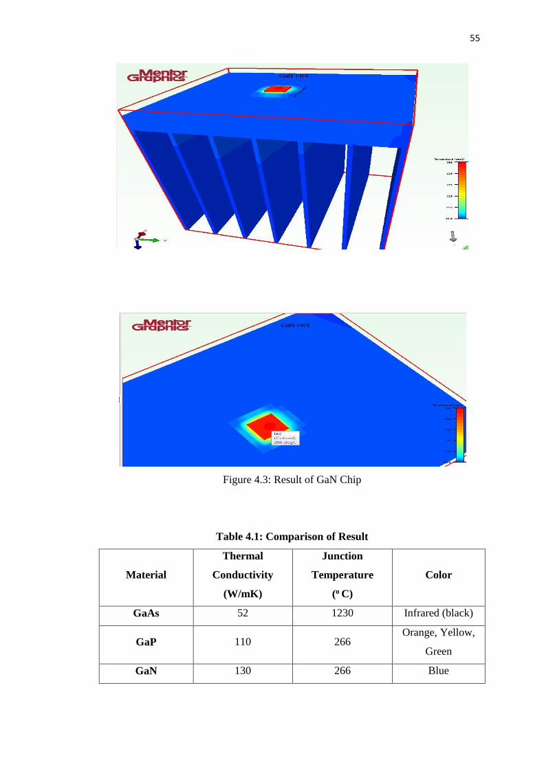
4.3 Result of GaN LED Chip 55
4.4 Result of GaN LED Chip Module with TIM
Added 57
4.5 Effect of applying TIM 58

XIV
4.6 Result of GaN LED Module with MCPCB
Substrate 59
4.7 Result of GaN LED Module with DBC substrate 60
4.8 Multiple-Chips LED Module with Two Chips 62
4.9 Multiple-Chips LED Module with Four Chips 62
4.10 Multiple-Chips LED Module with Eight Chips 63
4.11 Simulation Result of Multiple-Chips LED Module
with Distance between LED Chips of 2mm 64
4.12 Simulation Result of Multiple-Chips LED Module
with Distance between LED Chips of 8mm 64
4.13 Simulation Result of Eight Multiple-Chips LED
Module with Rectangle Orientation 65
4.14 Simulation Result of Eight Multiple-Chips LED
Module with Triangle Orientation 66
4.15 Simulation Result of Eight Multiple-Chips LED
Module with Circle Orientation 67
4.16 Simulation Result of Eight Multiple-Chips LED
Module with Straight Line Orientation 68
4.17 Heat Sink Used Before Modification 70
4.18 Result of LED Module with Area of 40 mm2 70
4.19 Result of LED Module with Area of 80 mm2 71
4.20 Result of LED Module with Area of 100 mm2 71
4.21 Result of LED Module with Thickness of 0.1mm 74
4.22 Result of LED Module with Thickness of 1mm 75
4.23 Result of LED Module with Thickness of 10mm 76
4.24 Result of LED Module with 2 Fins 78
4.25 Result of LED Module with 4 Fins 78
4.26 Result of LED Module with 5 Fins 79
4.27 Result of LED Module with 11 Fins 79
XV
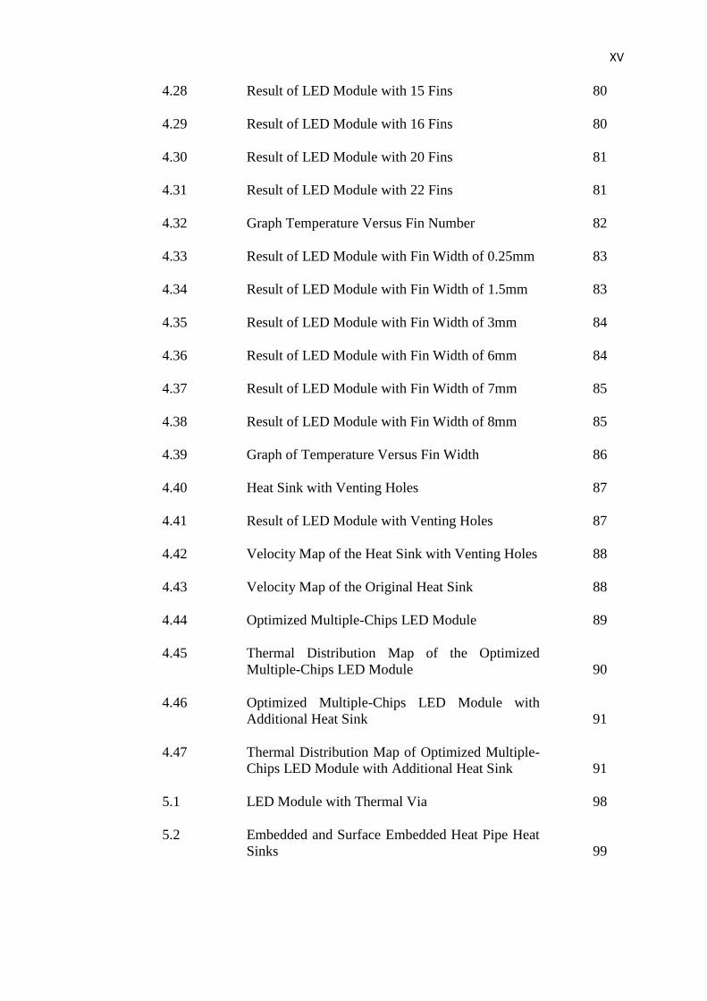
4.28 Result of LED Module with 15 Fins 80
4.29 Result of LED Module with 16 Fins 80
4.30 Result of LED Module with 20 Fins 81
4.31 Result of LED Module with 22 Fins 81
4.32 Graph Temperature Versus Fin Number 82
4.33 Result of LED Module with Fin Width of 0.25mm 83
4.34 Result of LED Module with Fin Width of 1.5mm 83
4.35 Result of LED Module with Fin Width of 3mm 84
4.36 Result of LED Module with Fin Width of 6mm 84
4.37 Result of LED Module with Fin Width of 7mm 85
4.38 Result of LED Module with Fin Width of 8mm 85
4.39 Graph of Temperature Versus Fin Width 86
4.40 Heat Sink with Venting Holes 87
4.41 Result of LED Module with Venting Holes 87
4.42 Velocity Map of the Heat Sink with Venting Holes 88
4.43 Velocity Map of the Original Heat Sink 88
4.44 Optimized Multiple-Chips LED Module 89
4.45 Thermal Distribution Map of the Optimized
Multiple-Chips LED Module 90
4.46 Optimized Multiple-Chips LED Module with
Additional Heat Sink 91
4.47 Thermal Distribution Map of Optimized Multiple-
Chips LED Module with Additional Heat Sink 91
5.1 LED Module with Thermal Via 98
5.2 Embedded and Surface Embedded Heat Pipe Heat
Sinks 99

XVI
LIST OF SYMBOLS / ABBREVIATIONS
R j-a total thermal resistance, K/W
K thermal conductivity, W/mK
Tj junction temperature, K
Ta ambient temperature, K
Tb board temperature, K
Pth thermal power dissipated by the LED module, W
R die thermal resistance of LED chip, K/W
R die attached thermal resistance of die attached, K/W
R slug thermal resistance of slug, K/W
R solder paste thermal resistance of solder paste, K/W
R substrate thermal resistance of substrate, K/W
R TIM thermal resistance of TIM, K/W
R heat sink thermal resistance of heat sink, K/W
tdie thickness of the LED chip, m
kdie thermal conductivity of the LED chip, W/mK
Adie cross section area of the LED chip, m2
T(x,y,z) temperature of the LED chip at coordinate x,y,z, K
N number of the LED chip
θi total temperature excess of the module, K
Q total heat dissipation power, W
Ρ density, kg/m3
t time, s
p pressure, kPa
g gravity, m/s2
µ viscosity, m2/s
Vf forward voltage of the LED module, V
If current flow through the LED module, A

XVII
H thermal coefficient (percentage of power converted to heat), %
CFD computational fluid dynamic
LED light emitting diode
COB chips on board
TIM thermal interface material
PCB printed circuit board
MCPCB metal core printed circuit board
DBC direct bond copper
AlN aluminium nitrate
GaN gallium nitrate
GaAs gallium arsenide
GaP gallium phosphide

CHAPTER 1
INTRODUCTION
1.1 Background
Nowadays, the demand of LED (light emitting diode) has increased sharply owing to
its advantages over the fluorescent light bulb and incandescent light bulb. LED is a
power saving, long life time and environment friendly device. Besides, it is small in
size and easy to control. Usually, a LED only need 3V of voltage to produce high
luminous light output and the LED starts up quickly with low temperature and less
noise. On the other hand, fluorescent light bulb requires a starter to start up the bulb
and the starter consumes large amount of power (nearly 100 kW) during the start up
process. It wastes a lot of energy and the life span is short if the fluorescent light bulb
is switching on and off frequently. Therefore, LED is overriding traditional
fluorescent light bulb in this past few years.
However, LED also has some disadvantages. The main disadvantage of LED
as a light source is the low light lumen. Most of the researches showed that LED only
converts 15% to 30% of the input power into light energy. In other word, it is about
80% of the input power been converted into heat energy. This high heat output
reduces the light luminance and the life span of the LED sharply. The condition
becomes worse when the LED was packaged into multiple-chips LED module which
has smaller size and high packaging densities. The heat generated is unpredictable
and module may be seriously damaged without efficient heat dissipation. Thermal
management is thus important to keep the junction temperature of the LED low. It

would indirectly enhance the light output quality and prolong life time of the LED
module.
Besides thermal management, it is also important to predict the thermal
performance of LED during the design phase. This would help the designer in
designing LED modules which has high luminous light output and good heat
dissipation ability. One of the most common methods used for the prediction of
thermal performance is computational fluid dynamic (CFD) modeling and simulation.
The simulation is fast and cost saving as designer can model their design in the
software directly instead of building their prototype by hardware. This also allows
the designer to examine their designed module under extreme condition by setting
the junction temperature above the specified temperature that is typically limited by
the manufacturers. Besides, CFD can map the temperature distribution and measure
the junction, ambient and surface temperatures of the module accurately. Designers
may also change their design directly based on the generated results in order to
optimize the thermal performance of their design.
The CFD software named FLOTHERM would be used in this project.
FLOTHERM is user friendly because it has a large library of predefined thermal
models. Moreover, user can add in electronic and thermal components such as fans,
heat sink, heat pipe and many others to simulate the thermal performance of the
model. In addition, the simulation helps user to obtain the detailed graphical result
such as temperature distribution of the module.
1.2 Problem statement
In this day and age, LED chips are mounted near each other directly on a substrate.
This type of LED modules has improved the lightning system technology because it
is smaller in size and provides higher intensity yet uniform light output. However,
the small size, high packaging densities with high power output LED modules
generate large amount of heat. If the heat generated is not able to dissipate well then

it will damage the module seriously. Besides, large amount of energy is wasted in the
form of heat energy and this reduces the energy efficiency of the module.
As a measure to the abovementioned disadvantages, various studies on
thermal management of LED module have been carried out. The main objective of
the thermal management studies is to remove the heat effectively. However,
effectiveness of thermal management researches in real life relies on a number of
technical problems which are not fully understood.
First, it is not easy to measure the junction temperature of real LED modules.
Typically thermocouples and IR camera are used to measure the junction temperature.
However, the results may not be accurate and precise due to the small size of the
LED module. This is due to the fact that the thermocouple is placed next to the chip
that covered by lens, whereas the IR camera can only record the surface temperature
of the LED module. This would cause the variants in result from that taken on the
actual heating point (Shi et al., 2015). Besides, the result could be affected by the
external environment such as movement of air, humidity, intensity of light and many
others. Moreover, the designer cannot observe the heat flow and heat spot of the
module. Without the heat flow and heat spot parameters, the designer cannot modify
his design because he does not know which part of the module has problems. This
may prohibit the efficient removal of heat from the module.
It is a time consuming task for the designer to manufacture new LED
modules each time he modified his design. Large amount of money is required to
build the LED modules repeatedly. Besides, it is almost impossible to build two
identical LED modules in real life. The quality of heat flow may change in the new
developed module since it depends strongly on the quality of material used.
Roughness of the material, air bubbles in the thermal grease layer, cracks in the die
attached layer could change the result. Thus, the designer may not able to perform
the comparison between two different modules. Moreover, designer cannot change
the parameter of the LED module because variants may occur if the parameters of
the design exceed the parameter set by the manufacturers. As a result, designer may
miss to find out the factors that affect the thermal management of the module.

Thermal analysis and module design using FLOTHERM simulation is able to
solve all the problems mentioned above. The junction temperature, ambient
temperature and surface temperature of the module can be determined easily after the
module was designed. The software also allows designer to zoom into any parts of
the module to obtain the temperature. Furthermore, the result is more stable because
it will not be affected by the external environment. Thermal distribution map and
heat sport of the module can also be generated. Moreover, the designer can modify
his design easily by changing the key parameters while keeping other parameters
unchanged. This allows the module to function under extreme conditions so as to
observe some possible effects that would occur.
1.3 Aim and Objectives
The objectives of the project are shown as follow:
i) To develop a detailed component level computational model of the multiple-
chip LED package module using CFD software.
ii) To study the factors that affect the thermal resistance of the LED module
such as thermal conductivity of material, LED chips arrangement and heat
sink design.
iii) To model a multiple-chip LED module that has high luminous light output
and good heat dissipation properties.

1.4 Outline
This report consists of five chapters and short summary for each chapter is discussed
in this section.
Chapter 1 describes the background of the LED module and the FLOTHERM
CFD software used in the present study. Besides, it reports the importance of using
the FLOTHERM software in studying the thermal management of a LED module.
This chapter also discusses the problem statement of the thermal analysis and the
advantages of using the CFD software to solve the actual problem in real life thermal
analysis. The objectives that provide directions for this project are stated in this
chapter.
Chapter 2 discusses the literatures from various researchers. The review of
the operation of LED, type of LED, thermal resistance, thermal conductivity of the
material available and the effect of thermal conductivity on thermal management are
summarized in this chapter. Moreover, the structure of the LED modules designed by
other researchers and designers are discussed here.
Chapter 3 reports the methodology of this study. The software
implementation of the CFD software is described, in terms of the steps to develop the
detailed LED module in CFD software and the dimension and material of each layer
of the LED module.
Chapter 4 analyses the results of the simulation. Discussion of the simulation
results will be presented here too. The discussion includes the factor that affect the
thermal management performance of the LED module, namely the thermal
conductivity of the material, LED arrangement and heat sink design. The optimum
parameters used in develop multiple-chip LED module that has high luminous light
output and good heat dissipation properties are subsequenly suggested in this chapter.
Chapter 5 indicates the concluding remark and recommendation of the future
work to improve the module design. The summary of the project also presented here.

CHAPTER 2
LITERATURE REVIEW
This chapter explains the main concept and theory used throughout the project.
Besides, it also discusses some researches conducted by various researchers so as to
give a clearer overview about this project. Their implementation methods and
achievements are compared in this chapter.
2.1 Light Emitting Diode (LED)
LED is a semiconductor light source. The LED emits light in a way different from
other light bulb because it does not have a filament. The LED produces light when
the semiconductor crystal is excited by a suitable voltage supplied to it. This
phenomenon is known as electroluminescence.
LED exhibits the electroluminescence phenomena as it is a p-n junction diode.
The LED is built using the crystal (poor conductor) that is doped to reduce it
conductivity. Doping is the process of adding impurities to a material and there are
two kind of doping. N-type doping adds one more electron on the semiconductor and
makes the semiconductor negatively charged, whereas P-type doping adds one extra
hole on the semiconductor that makes the semiconductor positively charged. A LED
is built by bonding a section of N-type material to a section of P-type material. This
arrangement causes voltage to flow in one direction only. When no voltages apply to
the LED, electron from the N-type material will fills the hole on P-type material.

7
This causes negative ion forms on the P-type material and positive ion forms on the
N-type material. It creates a charge and forms the depletion region. The depletion
region creates a large electric field that inhibits the flowing of electron to the P-type
material. As a result, the semiconductor fails to conduct electricity. When forward
bias voltage is applied to the semiconductor (negative terminal on the N-type
material and positive terminal on the P-type material), the free electron at the N-type
material is repelled by the negative charged of the electrode. The repletion force that
stronger than the opposing electric field force of the depletion region pushes the
electron to the hole on the P-type material causing current to flow again. To explain
it in a simple method, a LED can light up when sufficient voltage is applied. This is
because the electron from the N-type material is able to combine with the hole from
P-type material at the P-N junction. This combination releases the energy in the form
of photon and the energy is converted into light energy.
Figure 2.1: Unbiased P-N Junction
Layer of
negative ion
positive ion
Layer of positive
ion
positive ion
free
electron
hole
Depletion
region
positive
ion
P-type
material
positive
ion
N-type
material
positive
ion
8
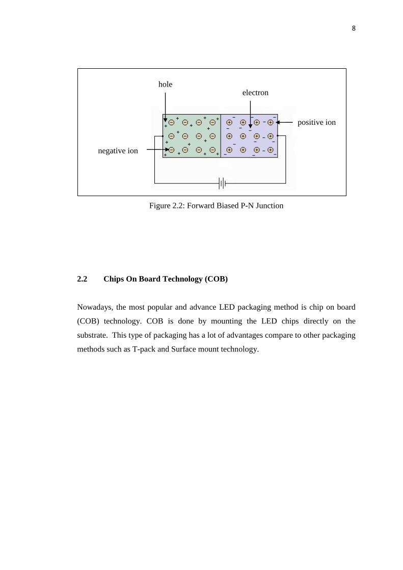
Figure 2.2: Forward Biased P-N Junction
2.2 Chips On Board Technology (COB)
Nowadays, the most popular and advance LED packaging method is chip on board
(COB) technology. COB is done by mounting the LED chips directly on the
substrate. This type of packaging has a lot of advantages compare to other packaging
methods such as T-pack and Surface mount technology.
hole electron
positive ion
negative ion

9
Table 2.1: Type of Packaging
LED
type
T-Pack Surface Mount Chip on Board
Device
image
Package
Array
(10mm x
10mm)
Density 9 LEDs 40 LEDs 342 LEDs
Array
power 0.4 Watts 4 Watts 68 Watts
From the Table 2.1, we can see that the number of LEDs can be mounted on a
10mm x 10mm substrate (total 342 LEDs) using COB method is much higher than
that of using the other two methods. Increases in number of LED built on the module
will increase the light output of the module. This also implies that COB technology
has ability to improve the operation of lighting system since COB LED module gives
high luminous and uniform output with a smaller size.
2.3 Measuring the Brightness of LED
The measurement of brightness for LED module is different from the fluorescent
light. In fluorescent light bulb, we usually look on watts to determine the output
brightness. Actually, the wattage is not use to measure the brightness but use to
measure the amount of energy drawn by the bulb. However, it is still acceptable to
compare the brightness of bulb with wattage for fluorescent light bulb but not for
LED.
In LED, lumen is used to measure the brightness for LED. The higher the
lumen, the brighter the output of the LED. The lumen (lm) is the SI unit for luminous

10
flux. It is use to measure the total amount of light which are visible by human eye
that emits from a light source. It is different from radiant flux which measures the
total amount of wave emits, independent on human eye ability to receive it.
Therefore, a good LED is LED which emit high lumen of light intensity with low
power input.
Moreover, the brightness of the light may be also affected by the color of the
light although they have same lumen. Light color is measured in Kelvin (K). A lower
Kelvin temperature is called hot light because its spectrum has a lot of yellow and
red color which look like a flame. The hot light appears yellow. It perceived as
comfortable and suitable for general lighting in houses. On the other hand, higher
Kelvin (more than 5000 K ) light is called cold light. Cold light appears white and it
is brighter than hot light. It is suitable to use in kitchen and work space.
2.4 Thermal Management
High power LED module is commonly used as light source nowadays. Due to low
luminous output for a single chip high power LED module, LED arrays with
multiple-chip package are introduced for general illumination. However, these arrays
generate large amount of heat. If the heat cannot dissipate well, the luminous and life
span of the LED module will be greatly reduced. Therefore, thermal management is
very important during the design process of LED module (Shi et al., 2015). Thermal
management is the technique that uses different kind of temperature monitoring
devices and cooling methods to control the overall temperature of the module. For
LED module, the thermal management focuses on lowering the junction temperature.
This is because high junction temperature of LED module will induce thermal
activation of non radioactive electron-hole recombination and cause increases in
defect responsible due to increase in non radioactive recombination. The increase in
defect responsible will cause decrease in luminous and life span of the LED module
(Chuang, et al., 1997). Thus, it is important to maintain the junction temperature of

11
the LED module low during the operation period so as to prolong the life span and
enhance the quality of the light output.
2.4.1 Thermal Resistance
Thermal resistance is the key factor that affects the junction temperature of the LED
module. High thermal resistance leads to high junction temperature (Liu et al., 2014).
In the past few years, various researches had been carried out by designers and
thermal engineers in order to reduce the thermal resistance as well as the junction
temperature of the LED module. Before the researches are discussed, it is important
to understand some of technical terms that always appear in thermal management
design. Thermal resistance is the rate of temperature increase due to increase in
dissipated power. It is also measures the capability of the material to dissipated heat
according to the article in 2011 by OSRAM. The higher the thermal resistance, the
lower the capability of the material to dissipate heat. Thermal resistance in LED is
caused by the temperature difference between the junction temperature and the
ambient temperature. The temperature difference creates pressure in the junction and
the pressure restricts the heat flows from LED chip to the surrounding. As a result,
more and more heat accumulates at the junction and cause increase in the junction
temperature. Thermal resistance is calculated based on the formula:
𝑅𝑗−𝑎 =(𝑇𝑗 − 𝑇𝑎)
𝑃𝑡ℎ
(2.1)
where
R j-a = total thermal resistance, K/W
Tj = junction temperature, K
Ta = ambient temperature, K
Pth = thermal power dissipated by the LED module, W(Vakrilov, et al)

12
From the formula, thermal resistance changes proportional to temperature
difference between junctions and ambient. Thus, lower thermal resistance decreases
the temperature difference which also indirectly decreases the junction temperature.
Next, in order to predict the junction temperature of the LED chip before the
module is designed, the total resistance between the LED chips and the ambient (Rj-a)
must be calculated. Figure 2.3 shows the thermal resistance found in a LED module.
Figure 2.3: Thermal Resistance Found in a LED Module
From Figure 2.3, the total thermal resistance found in the single LED chip module
can be expressed using the formula:
𝑅𝑗−𝑎 = 𝑅𝑑𝑖𝑒 + 𝑅𝑑𝑖𝑒 𝑎𝑡𝑡𝑎𝑐ℎ + 𝑅𝑠𝑙𝑢𝑔 + 𝑅𝑠𝑜𝑙𝑑𝑒𝑟 𝑝𝑎𝑠𝑡𝑒 + 𝑅𝑠𝑢𝑏𝑠𝑡𝑟𝑒𝑎𝑡𝑒 + 𝑅𝑇𝐼𝑀
+ 𝑅ℎ𝑒𝑎𝑡 𝑠𝑖𝑛𝑘
(2.2)
Next, all the low conductivity materials such as die attach, solder paste and TIM is
removed from the equation. The simplified total thermal resistance can be estimated
as
𝑅𝑗−𝑎 = 𝑅𝑑𝑖𝑒 + 𝑅𝑠𝑙𝑢𝑔 + 𝑅𝑠𝑢𝑏𝑠𝑡𝑟𝑒𝑎𝑡𝑒 + 𝑅ℎ𝑒𝑎𝑡 𝑠𝑖𝑛𝑘
(2.3)

13
By assuming uniform heat flux on the top of the chip, the thermal resistance of the
LED chip can be described with one dimensional thermal resistance model for heat
diffusion, which is
𝑅𝑑𝑖𝑒 =𝑡𝑑𝑖𝑒
𝑘𝑑𝑖𝑒 𝐴𝑑𝑖𝑒
(2.4)
where
Rdie = thermal resistance of the LED chip,K/W
tdie = thickness of the LED chip,m
kdie = thermal conductivity of the LED chip, W/mK
Adie = cross section area of the LED chip,m2
For thermal resistance of slug, substrate and heat sink, the formula used is same as
the equation (2.4) but replacing all the parameter t, k and A with the parameter for the
slug, substrate and heat sink.
To calculate the thermal resistance of the multiple-chip LED module, general
analytic solution based on separation variable can be used. The solution for the
temperature distribution of the heat sink which used to calculate the temperature of
the multiple-chips LED module is
𝑇(𝑥,𝑦,𝑧) − 𝑇𝑎 = ∇𝑇 = ∑ 𝜃𝑖(𝑥, 𝑦, 𝑧)
𝑁
𝑖=1
(2.5)
where
Ta = ambient temperature, K
T(x,y,z) = temperature of the LED chip at coordinate x,y,z, K
N = number of the LED chip
θi = total temperature excess of the module, K (Cheng et al., 2010)
The θi for the surface temperature distribution of the LED module at z=0 is
𝜃𝑖(𝑥, 𝑦, 0) = 𝐴0
𝑖 + ∑ 𝐴𝑚𝑖 cos(λx)∞
𝑚=1 + ∑ 𝐴𝑛 𝑖 cos(𝛿𝑥) +∞
𝑛=1
∑ ∑ 𝐴𝑚𝑛𝑖∞
𝑛=1∞𝑚=1 cos(λx) cos(δx)
(2.6)

14
After solving the Fourier coefficient Am, An, and Amn, the total resistance of the N N
array multiple-chip LED module can be calculated using the formula
𝑅𝑗−𝑎 = 𝑅𝑑𝑖𝑒 + 𝑅𝑠𝑙𝑢𝑔 + 𝑅𝑠𝑢𝑏𝑠𝑡𝑟𝑒𝑎𝑡𝑒 +
𝑁 × 𝑅ℎ𝑒𝑎𝑡 𝑠𝑖𝑛𝑘
(2.7)
The equation can be obtained by assuming the innermost gives the highest junction
temperature
𝑁 × 𝑅ℎ𝑒𝑎𝑡 𝑠𝑖𝑛𝑘 = 𝑇(𝑥,𝑦,0)
𝑁𝑄
(2.8)
where Q is the total heat dissipation power measured in Watt (W).
2.4.2 Junction temperature, Board Temperature and Ambient Temperature
Difference between junction temperature, board temperature and ambient
temperature must be firstly understood. Junction temperature is the highest
temperature in the package of the device when the device is operating (Altera, 2012).
Based on the article from electronic engineering journal, junction temperature is the
internal temperature of the component itself (LED chip) which strongly affects its
functionality and reliability. It can also refer as the hottest temperature on the LED
module due to its power dissipation during operation. Thus, the most accurate way to
measure the junction temperature is to measure the LED chip itself.
Next, board temperature is the temperature adjacent to the LED chip. The
measurement point of the board temperature should be less than 1 mm away from the
centre of the LED chips. Figure 2.4 shows the ideal measuring point for the board
temperature.

15
Figure 2.4:Ideal Measuring Point for Board Temperature
After the board temperature is measured, junction temperature can be calculated
using the formula:
𝑇𝑗 = 𝑇𝑏 + (𝛹𝑗𝑏 ∗ 𝑃𝑡ℎ) (2.9)
where
Tj = junction temperature, K
Tb = board temperature, K
Ψjb = Psi-jb, K/W
In equation (2.2), a new term is introduced which is Psi-jb. The Psi-jb is
almost same as the Theta-jb (θjb, thermal resistance). When calculating Theta-jb, the
heat is assumed to flow from the junction to the board. On the other hand, when
calculating the Psi-jb, the heat is assumed to flow through top and side of the chip.
Therefore, the value for Psi-jb is smaller than Theta-jb because the temperature
difference is divided by the full power instead of the power from the source of the
temperature difference (XILINX, 2013). Figures 2.5 and 2.6 show the simplified
form of the difference between Theta and Psi.
Measure the board
temperature at a
distance less than 1
mm from the chip

16
Figure 2.5: Formula and Method to Find Theta
Figure 2.6:Formula and Method to Find Psi
From the Figures 2.5 and 2.6, specific heat flow path must be determined before
calculating the theta. On the other hand, the specific heat flow path is not important
when calculating psi. This is because the total heat in the system is used to calculate
the Psi (Stout, 2008).
Psi (Ψ)
Ψxy=T𝑙𝑜𝑐𝑎𝑡𝑖𝑜𝑛 𝑥−Tlocation 𝑦
Power toal device
We only know the
total device power
Theta (θ)
θxy=T𝑙𝑜𝑐𝑎𝑡𝑖𝑜𝑛 𝑥−Tlocation 𝑦
Power path𝑥−𝑦
The actual heat
path is known

17
Moreover, ambient temperature is the temperature that distant away from the
LED chip, hence it is not affected by the component heat contribution. As for
example, if the LED is packaged in housing, the ambient temperature is the
temperature outside the housing. From the example and explanation, ambient
temperature can refer to the air temperature inside or outside the LED module.
Figure 2.7 shows some of the measuring point for the ambient temperature.
Figure 2.7: Eight Different Measuring Points for Ambient Temperature
There are eight potentially different ambient temperature measuring points
(Romig, 2010). The ambient temperature is different when the ambient temperature
is measured at different measuring points. Therefore, calculating the junction
temperature using the ambient temperature is less accurate and shall not be used.
Final System (Airflow optional)
1
2 5
4
4
3
System testing on bench or in oven
5
6
7,8

18
2.4.3 Thermal Conductivity and Thermal Management Product
Thermal conductivity is the ability of a material to conduct heat. The higher the
thermal conductivity of the material, the easier the material conducts heat. Thermal
management consists of three categories namely package level, board level and
system level. In package and board level, selection of the material for die structure,
die bonding and substrate is very important (Yang et al., 2013) Ideally, to have a
good thermal management performance, materials which have high thermal
conductivity was chosen when building the module. In this session, some researches
that involve the application of thermal conductivity of material of to improve the
thermal management performance of the LED module are discussed. Besides, some
improvements have been done by researchers to enhance the thermal management
performance of LED module without increasing the cost and size of the LED module.
The first research discussed is about thermal conductive substrate. Based on
an article on lighting technology, Rich Wessel and Kurt Roberts found that thermal
conductive substrate is the key factor in improving the thermal management
performance of LED. They have carried out the research to determine the suitable
material to make the circuit board. They replaced the traditionally used aluminum
based FR-4 boards circuit board with metal core laminated board (MCB) such as
DuPontTM CooLamTM thermal substrate. DuPont has the polyimide content which is
commonly applied to many industries field. It is due to the fact that it can maintain
the good physical, electrical and mechanical properties over a wide range of
temperature. Due to the advantage of the polyimide layer in the DuPontTM
CooLamTM thermal substrate, they are used as good insulated metal substrate for
high power LED module. Moreover, the thin polyimide layer has very low thermal
resistance together with thin dielectric layer that allow heat to dissipate in a small
package LED module. At the end of their research, they found that thermal
management performance of the LED modules with MCB substrate is better that
LED modules with FR-4 substrate due to thin dielectric insulating layer according to
the article in 2012 written by DuPontTM CooLamTM.
Next, metal core printed circuit board (MCPCB) is also used as a substrate
because it provides high thermal management performance. MCPCB board has

19
aluminum or copper metal core and insulating layer on top. The metal core is used to
provide mechanical support and help in heat dissipation. However, the thermal
performance of MCPCB is lower than MCB due to the high thermal resistance of the
insulating layer. In the research of Eveliina Juntunen, copper core MCPCB with
thermal vias is introduced. The copper core MCPCB consists of microvias through
the FR4 insulating layer. Juntunen found the microvias provide an effective path for
the heat from the LED chip to be dissipated through high thermal resistance
insulating layer. Based on the result of the research, the thermal management
performance of the MCPCB with microvias is better than the thermal management
performance of aluminum MCPCB. Figures 2.8 and 2.9 show the structure of the
MCPCB with microvias and a typical MCPCB (Juntunen et.al, 2014).
Figure 2.8: LED Module with Copper MCPCB with Vias
Figure 2.9: LED module with Aluminum MCPCB
Die attach
Au contact
Au wire bonding
Al2O3 1.27mm
LED chip
Thick film
Ag
FR4,70µm
Cu, 2.0mm
Au contact
Au wire bonding
LED chip
Die attach
Cu coil,35µm
Microvia

20
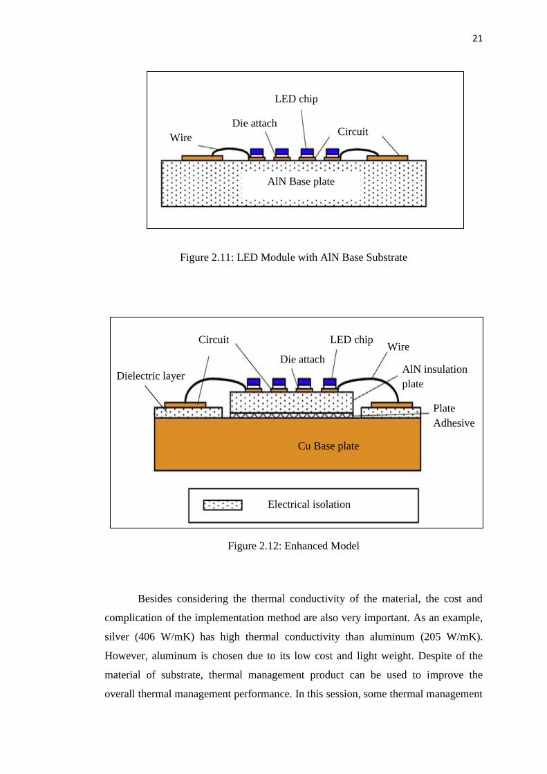
Next, aluminum nitrate (AlN) is a good material to be used as substrate
because it has high thermal conductivity and electric insulation. These properties
make AlN substrate thinner than the MCPCB substrate because MCPCB substrate
requires additional layer for the insulating material. Besides, the AlN has low
thermal resistance because it does not require the high thermal resistance insulating
material that needed in MCPCB. A research was carried out by Yin et al. for thermal
analysis on multiple-chip LED module with different types of ceramic substrate.
They found the module with AlN substrate has better heat dissipation properties than
aluminum and aluminum 103 based substrate (Yin et al., 2010) However, it is not
suitable to use AlN alone to build the whole substrate because it is very expensive
and brittle. In the research of Jeong (Jeong et al., 2015), instead of using the AlN as
the whole substrate, he has used the AlN as insulating material between the LED
chips and the copper substrate. The heat management performance of the enhanced
module is compared with AlN substrate based LED module and copper substrate
base module. He found out that the enhanced model provides good thermal
dissipation, electric insulation and high luminous output. Moreover, the cost and the
risk of brittleness of the AlN material can be overcome.
Figure 2.10: LED Module with Copper Base Substrate
Wire
Die attach LED chip
Circuit Dielectric layer
Cu base plate
21
Figure 2.11: LED Module with AlN Base Substrate
Figure 2.12: Enhanced Model
Besides considering the thermal conductivity of the material, the cost and
complication of the implementation method are also very important. As an example,
silver (406 W/mK) has high thermal conductivity than aluminum (205 W/mK).
However, aluminum is chosen due to its low cost and light weight. Despite of the
material of substrate, thermal management product can be used to improve the
overall thermal management performance. In this session, some thermal management
Dielectric layer
Circuit
Die attach
LED chip Wire
AlN insulation
plate
Plate
Adhesive
Cu Base plate
Electrical isolation
Wire
Die attach
LED chip
Circuit
AlN Base plate

22
products that can help to improve the conduction of heat in LED module are
discussed.
Thermal interface material (TIM) is widely used to improve the thermal
management performance of LED module. This material is used to fill the air gap
between the mating surface of the module and heat sink. Usually, heat sink is always
used in LED application to increase the surface area of the LED module so as to
improve the heat dissipation ability. However, air gaps will present at the interface of
the LED module and heat sink. This greatly reduces the efficiency of heat transfer.
Thus, TIM is used to fill the air gaps to reduce the thermal resistance between the
LED module and the heat sink. Next, thermal conductive encapsulation resin is also a
good thermal management product. In addition to protecting the LED module from
environment attack, it also helps to dissipate the heat generated in the LED module to
the surrounding (Electrolube, 2015).
2.5 Computational Fluid Dynamic (CFD) software and FLOTHERM
Computational fluid dynamic (CFD) software uses numerical analysis and algorithms
to analyze problem involving fluid flow. Usually, computer is used to calculate and
simulate the interaction of the fluid (liquid and gas) with the boundary condition
(external environment of the model set by the user). Nowadays, CFD software is
widely use in thermal analysis and design of LED module. This is because CFD
software is accurate in simulation of LED module that involves fluid flow, heat
transfer and radiation processes (Ling, 2010). Besides, it is better to use CFD
software to model the thermal analysis of LED module compared to Finite Element
Methodology (FEM) software because FEM only can perform only the heat
conduction simulation while CFD software is capable in modeling a thermal
environment that close to reality. CFD software allows user to simulate a module that
consists of cooling assemblies and the air flow properties inside the module.
Moreover, the external environment of the module such as the air flow, humidity,
temperature can be set to analysis the heat dissipation of the module through
conduction, convection and radiation (Poppe et al., 2008).

23
In the thermal processing, the Navier Stokes equation is fundamental
mathematical formula for the fluid motion in CFD software. Besides, the heat
transfer equation is used to solve the energy equation involving the heat transfer in a
fluid system. The CFD software also provides a lot of models such as Turbulence
Model, Eddy Viscosity Model, Reynolds Stress Model, Radiation Model and many
others (Nortan, Brijesh and Sun, 2013). The simulated physical interface provided by
the CFD Models allows user to model the most aspects of fluid flow single phase
flow, non-isothermal flow and compressible flow. With the models provided, the
heat and air flow in the LED module can be simulated accurately.
In past few years, a lot of researches have been done to prove the accuracy of
the result generated using CFD software on thermal analysis. In the work of Andras
Poppe, the JESD 51-1 static measurement is compared with CFD simulation on
thermal analysis of LED module. He found that both methods are different in term of
required time and other factors. He also claimed that both methods give a close
result but different trade off should be made between the thermal simulation and
physical testing. Chi et al. performed the thermal analysis of high power LED
module that associated with heat sink using the CFD simulation including the heat
transfer correlation and radiation of heat transfer. The research of Weng shows that
detailed 3D CFD analysis can improve in the study of thermal management of the
LED module. These researches show that CFD software is becoming important and
popular to be used in study of thermal management of LED module.
There are various CFD softwares such as OPENFOAM, OPENFLOWER,
FLASH ANSYS and many others. All these softwares work best in different kind of
application. Thus, appropriate software must be used in order to get an accurate
result. In this project, the CFD simulation software used is FLOTHERM.
FLOTHERM is a CFD software created by Mentor Graphic. It is suitable to use in
predict air flow, temperature and heat transfer of component in a system.
FLOTHERM has a user friendly operation interface that allows users to design their
module easily. It also has localized grid feature that support integrally matched,
nested non-conformal grid interface between different parts of the solution domain.
This feature allows accurate simulation result on each part of the module can be
produced. Furthermore, the integral model provided by FLOTHERM together with
24
the smart tool such as heat sink, heat pipe and PCB board allow users to create their
model easily. The module created can attached with different type of material, heat
dissipated, specific heat capacity, thermal conductivity and many other parameters.
With these features, a simulated module that is very close to real module can be
developed in a short time.
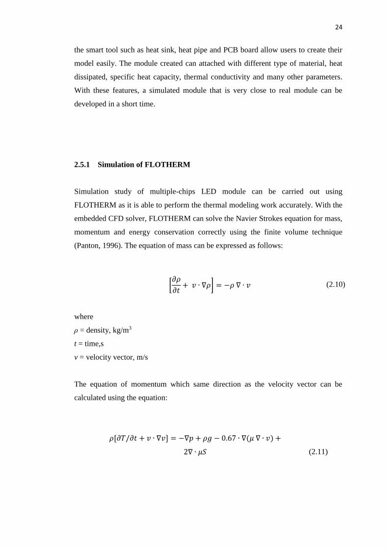
2.5.1 Simulation of FLOTHERM
Simulation study of multiple-chips LED module can be carried out using
FLOTHERM as it is able to perform the thermal modeling work accurately. With the
embedded CFD solver, FLOTHERM can solve the Navier Strokes equation for mass,
momentum and energy conservation correctly using the finite volume technique
(Panton, 1996). The equation of mass can be expressed as follows:
[𝜕𝜌
𝜕𝑡+ 𝑣 ∙ ∇𝜌] = −𝜌 ∇ ∙ 𝑣 (2.10)
where
ρ = density, kg/m3
t = time,s
v = velocity vector, m/s
The equation of momentum which same direction as the velocity vector can be
calculated using the equation:
𝜌[𝜕𝑇/𝜕𝑡 + 𝑣 ∙ ∇𝑣] = −∇𝑝 + 𝜌𝑔 − 0.67 ∙ ∇(𝜇 ∇ ∙ 𝑣) +
2∇ ∙ 𝜇𝑆
(2.11)

25
where
p = pressure,kPa
g = gravity, m/s2
µ = viscosity, m2/s
S = strain rate tension
After the equation of the mass and the momentum are solved, the thermal energy is
presented with the equation:
𝜌𝑐𝑝 [𝜕𝑇
𝜕𝑡+ 𝑣 ∙ ∇𝑇] = ∇ ∙ (𝑘∇𝑇) − 0.67 ∙ 𝜇(∇ ∙ 𝑣)2 + 2(𝜇𝑆 ∙ 𝑆) + 𝛽𝑇 ∙
[𝜕𝑝
𝜕𝑡+ (𝑣 ∙ ∇)𝑝]
(2.12)
where
T = absolute tempereature,K
k = thermal conductivity,W/mK
β = expensiveness
2.6 Researches
This section discusses the advantage and disadvantage of LED, structure of LED, the
factors that affect the thermal resistance, method to reduce the thermal resistance,
method to construct a detailed model of LED using CFD software.
Nikolay Vakrilov and his colleges have studied the effect of the topology of
LED chips on the thermal management of the LED module. They have simulated a
powerful COB LED module using CFD software and the thermal distributions at
different locations of the chip are examined. Besides, they have designed the LED
module with different kind of substrates which are Alumina (typical), Alumina
(94%), Alumina (96%) and AlN. The thermal efficiencies of the four LED modules
were examined. They also compared their result with real life thermal measurement

26
result and found out that the result produced using the CFD software is close to the
result of real life thermal measurement.
Mohammad Abdullah has studied the thermal efficiency of LED module with
different arrays of LED arrangement. The LEDs are arranged in array shape as
square, triangle, hexagon and circle. The junction temperature of the LED was
measured using a K-type thermocouple. This research is a good guideline for the
author to carry out the project. The author has carried out the same experiment based
on the methodology provided. Instead of using K-type thermocouple, the author used
CFD software to model the modules and obtained the result through simulation. The
author has verified the method used to model LED module and the result obtained
through FLOTHERM software before the author start to model his own LED module
(Abdullah et al., 2013)
Christenensen and Graham has examined the thermal behavior of high power
LED module due to different distances between the LEDs array and effect of
different material of package level and system level. They found out that when the
distance between the LED is close, the junction temperature of the LED is high while
the junction temperature of the LED is low when the distance between the LED is far
(Christenensen and Graham, 2007).

CHAPTER 3
METHODOLOGY
This chapter explains the method and process to implement this project. It includes
the detailed process and step which are deemed necessary in the simulation task.
Besides, the method of software design and development will be explained in this
chapter too.
3.1 Project overview
1. First, the title “Thermal simulation of multiple-chips LED module using
Computational Fluid Dynamic software“ is chosen from the list of topics for
final year project provided by Universiti Tunku Abdul Rahman.
2. After the proposal was submitted and approved by the supervisor, literature
studies were carried out to understand the structure of the LED module.
Related information about the modeling method for LED module using the
CFD software and that to measure the junction temperature were acquired
through online articles, online journals and research papers.

28
3. In this section, software implementation process using the CFD software will
be discussed in details. Figure 3.1 shows the progress and pace of the project
carried out.
Figure 3.1: The progress and pace of project
YES
Researches about the topic
Analysis and design of
LED module
Model the LED
module using CFD
software
Testing and
troubleshooting
Validate?
END
START
Selecting a topic
NO

29
3.2 Software Methodology
In order to study the thermal behavior of the multiple-chip LED module, a LED
module with multiple chips was modeled using CFD software named FLOTHERM.
After that, steady state thermal simulation was run to measure the junction
temperature. In the simulation, the conduction, convection and radiation heat transfer
process were included. In this project, the author has carried out thermal
management study considering three criteria, namely thermal conductivity of
material, LED arrangement and heat sink design.
The first step to carry out FLOTHERM study is to scope out the project and
define the data required. In this step, the author has studied the geometry and
physical properties of the real LED module provided by supervisor. The LED chip
used has a dimension of 1 mm 1 mm 0.5 mm. The forward voltage to the LED
chip, Vf is 3V and the current flow through the LED chip, If is 0.95A. The author
assumed that the thermal coefficient of the LED is 30%. This means 70% of the
power provided to the LED will be converted to heat energy. The estimated thermal
power loss of the LED chip is calculated using the formula:
Pth= Vf x If x H
(3.1)
where
Pth = estimated thermal power loss in the junction of the LED chip, W
Vf = forward voltage of the LED module, V
If = current flow through the LED module, A
H = thermal coefficient (percentage of power converted to heat),%
Note that the estimated thermal power loss of LED chip used throughout the project
is 2W.
The second step is to structure the LED module. When building the module,
smart parts such as heat sink, cuboids, hole and many others were considered. Smart
parts were used since they can be constructed parametrically, making it easier to

30
control the parameter of the object such as position and dimension. The module was
built with reasonable tolerance by avoiding small gaps between the smart parts to
improve the quality of the grid. After that, the smart parts were attached with
material and thermal power loss required. Once the module was developed, the
solution domain is set. The solution domain is the air around the module required to
be studied. It must be set bigger than the module developed in order to numerically
study all the thermal process such as temperature, heat flux, conduction process,
convection process and radiation process around the LED module. Figure 3.2 shows
the working environment of the FLOTHERM and the properties of the solution
domain used throughout the project are tabulated in Table 3.1
Figure 3.2: Working environment of FLOTHERM
Table 3.1: Properties of Solution Domain
Conductivity 0.02569 W/mK
Viscosity 1.824 10-5 N s/m2
Density 1.88 kg/m3
Specific heat capacity 1007 J/(kg K)
Expansibility 0.003421 K-1
Ambient temperature 25 oC
Pressure 1 Atm

31
This solution domain is an important parameter and it must be set accurately. A
slightly change in the properties of the solution domain will affect the result
simulated. Different size of solution domain was used in the three criteria as the
dimension of the LED modules used in each criterion is different. Monitor points
were added to the LED chip to allow the author to observe the changes in the
temperature of the LED chip when the solver is running. The cell size of the system
grid was then set. The smaller the cell size, the higher the accuracy. However, high
accuracy result required very long time to be generated because the simulation speed
depends on the performance of the computer. The cell size was set in a range of 0.01
mm to 194.2 mm. In this range, the result generated is accurate and the time required
to generate the result is reasonable. Localized grid feature was used at the LED chip
as junction temperature of the chip is one of the main factors. Localized grid feature
allows high resolution grid set at the LED chip to improve the accuracy of the
simulation result.
Once the module was finish developed the solver was set to run. The profile
window showed the residuals and the temperature of the monitoring points which are
the junction temperature of the LED during the solver process. Figure 3.3 shows the
result on the profile window. Although the FLOTHERM is powerful software, the
users must keep an eye on both the residuals and values of monitoring points. If all
the variables in the residual table does not reach zero at the end of the simulation,
steady solution is not converged and an inaccurate result might be produced
undesirably. User has to stop the simulation and fix the error. On the other hand, if
all the variables reach zero, steady solution is converged. The simulation result can
be viewed in Visual Editor to study the result in graphical or tabular format. Figure
3.4 shows the environment of the visual editor. In the visual editor, the temperature
and heat flux of each part of the module can be viewed.

32
Figure 3.3: Profile Window
Figure 3.4 Visual Editor
3.3 Study of Thermal Conductivity of Material
In this session, a single chip LED module was modeled. The module consists of one
LED that have a dimension of 1 mm 1 mm 0.5 mm. The thermal power
dissipated of the LED is 2 W. The LED was attached on a copper slug which has a

33
dimension of 5 mm 5 mm 0.5 mm. After that, the LED and slug is then disposed
on a substrate which has a dimension of 10 mm 10 mm 1 mm. The solution
domain used is 60 mm 70 mm 80 mm. Figure 3.5 shows the LED module design
layout.
Figure 3.5 LED module design layout
In this simulation, the LED module was placed on an aluminum heat sink. The
aluminum heat sink is with a size of 50 mm 55 mm 5 mm. It has 5 plate fins with
fin height of 50 mm and fin width of 1 mm. Table 3.2 shows the properties of heat
sink. Figures 3.6, 3.7, 3.8 and 3.9 show the dimension of the heat sink, dimension of
the fins and length of the fins, respectively. Besides, the LED module that was
attached directly on the heat sink is shown in Figure 3.10.
Table 3.2 Properties of Heat Sink
Dimension 50 mm 55 mm
Thickness 5 mm
Number of fin 5
Fin height 50 mm
Fin width 1 mm
Material Aluminum

34
Figure 3.6: Heat Sink View on X Plane
Figure 3.7: Heat Sink Viewed on Y Plane
50mm
5mm
50mm
mm
Solution
domain
Heat fin
5mm
55mm
50mm
1mm
Heat fin
Solution
domain

35
Figure 3.8: Heat Sink Viewed on Z Plane
Figure 3.9: 3D View of the Heat Sink
1mm
500mm
55mm
Solution
domain
Heat fin

36
Figure 3.10: 3D View of the LED Module
3.3.1 Thermal Conductivity of LED Chip
LED chip that manufactured using different type of materials were tested.
The layout of the LED modules is same as the layout shown in Figure 3.10. Table 3.3,
Table 3.4 and Table 3.5 show the properties of the LED modules studies in this
session.
Heat sink
LED chip
Substrate
Heat slug

37
Table 3.3: Properties of GaAs LED Module
Component Material Dimension
(mm)
Thickness
(mm)
Conductivity
(W/mK)
LED
Gallium
Arsenide
(GaAs)
1 1 0.5 52
Slug Copper 5 5 0.5 385
PCB substrate FR4 10 10 1 0.3
Heat sink
Number of fin=7
Fin height=50 mm
Fin width=1 mm
Aluminum 50 50 10 201
Table 3.4: Properties of GaP LED Module
Component Material Dimension
(mm)
Thickness
(mm)
Conductivity
(W/mK)
LED
Gallium
Phosphide
(GaP)
1 1 0.5 110
Slug Copper 5 5 0.5 385
PCB FR4 10 10 1 0.3
Heat sink
Number of fin=7
Fin height=50 mm
Fin width=1 mm
Aluminum 50 50 10 201

38
Table 3.5: Properties of GaN LED Module
Component Material Dimension
(mm)
Thickness
(mm)
Conductivity
(W/mK)
LED
Gallium
Nitrate
(GaN)
1 1 0.5 130
Slug Copper 5 5 0.5 385
PCB substrate FR4 10 10 1 0.3
Heat sink
Number of fin=7
Fin height=50 mm
Fin width=1 mm
Aluminum 50 50 10 201
3.3.2 Thermal Interface material (TIM)
A layer of thermal interface material (TIM) was added to the LED module as shown
in Figure 3.10, so as to study the effect of the TIM on the thermal management
performance. Figure 3.11 shows the design layout of the modified LED module and
Table 3.6 shows the property of modified LED module used.
Figure 3.11: LED Module Design Layout

39
Table 3.6: Properties of the LED Module
Component Material Dimension
(mm)
Thickness
(mm)
Conductivity
(W/mK)
LED Gallium
Nitrate (GaN) 1 1 0.5 130
Slug Copper 5 5 0.5 385
PCB substrate FR4 10 10 1 0.3
TIM Dow coning
TC-5022 50 50 0.025 4
Heat sink
Number of fin=7
Fin height=50 mm
Fin width=1 mm
Aluminum 1 1 10 201
3.3.3 Thermal conductivity of Substrate
Moreover, two different types of substrates namely MCPCB and DBC were studied.
Figure 3.12 and 3.13 show the layout LED module with MCPCB substrate and DBC.
Table 3.7 and 3.8 show the properties of the LED module with MCPCB substrate
and DBC substrate.

40
Figure 3.12: LED module with MCPCB Substrate Design Layout
Figure 3.13: LED Module with DBC Substrate Design Layout
LED
DBC copper
Bottom copper AlN substrate
Base plate
TIM
DBC
LED
Slug
MCPCB core
MCPCB
dielectric
MCPCB
conductor TIM
MCPCB

41
Table 3.7: Properties of the LED Module with MCPCB Substrate
Component Material Dimension
(mm)
Thickness
(mm)
Conductivity
(w/mk)
LED Gallium
Nitrate (GaN) 1 1 0.5 130
Slug Copper 5 5 0.5 385
MCPCB
core Copper 10 10 2 385
dielectric FR4,IT-180 10 10 0.07 0.88
conductor Copper 10 10 0.035 385
TIM Dow coning
TC-5022 10 10 0.025 4
Heat sink
Number of fin=7
Fin height=50 mm
Fin width=1 mm
Aluminum 50 50 10 201
42
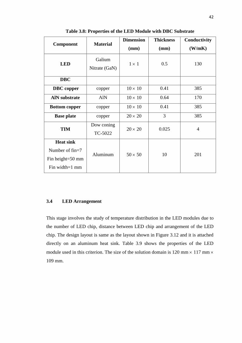
Table 3.8: Properties of the LED Module with DBC Substrate
Component Material Dimension
(mm)
Thickness
(mm)
Conductivity
(W/mK)
LED Galium
Nitrate (GaN) 1 1 0.5 130
DBC
DBC copper copper 10 10 0.41 385
AlN substrate AlN 10 10 0.64 170
Bottom copper copper 10 10 0.41 385
Base plate copper 20 20 3 385
TIM Dow coning
TC-5022 20 20 0.025 4
Heat sink
Number of fin=7
Fin height=50 mm
Fin width=1 mm
Aluminum 50 50 10 201
3.4 LED Arrangement
This stage involves the study of temperature distribution in the LED modules due to
the number of LED chip, distance between LED chip and arrangement of the LED
chip. The design layout is same as the layout shown in Figure 3.12 and it is attached
directly on an aluminum heat sink. Table 3.9 shows the properties of the LED
module used in this criterion. The size of the solution domain is 120 mm 117 mm
109 mm.

43
Table 3.9: Properties of the LED Module
Component Material Dimension
(mm)
Thickness
(mm)
Conductivity
(W/mK)
LED
Gallium
Nitrate
(GaN)
1 1 0.5 130
Slug Copper 1 1 0.5 385
MCPCB
core Copper 30 30 2 385
dielectric FR4,IT-180 30 30 0.07 0.88
conductor Copper 30 30 0.035 385
TIM Dow coning
TC-5022 30 30 0.025 4
Heat sink
Number of fin=12
Fin height=80 mm
Fin width=1.2 mm
Aluminum 100 100 10 201
3.4.1 Number of LED Chips
In this section, the author built three modules with different number of LED chips in
order to study the effect of number of LED chips on the average junction temperature
of the LED chips. Figure 3.14 shows the LED modules developed. The distance
between the LED chips was set to 2 mm for the three LED modules developed.

44
Figure 3.14: Z view of the LED module a) two LED chips module b) four LED chips
module c) eight LED chips module
3.4.2 Distance between the LED Chips
Modification was performed on the LED module which has eight LED chips that was
developed in the Section 3.4.1. Thermal simulation was carried out using the LED
module with different distance between the LED chips in 4 mm, 6 mm and 8 mm.
Figure 3.15 shows the Z-plane view of the modified module.
LED
MCPCB
a b
c

45
Figure 3.15: Z view of the 8 LED chips module with a) 4 mm distance
b) 6mm distance and c) 8mm distance
3.4.3 Orientation of LED chips
The eight LED chips modules was then modified to have different orientations.
Figure 3.16 shows the different orientation designed. In this session, author has
studied the effect of the orientation of LED chips to the average junction temperature
of the eight LED chips.
Figure 3.16: Z view of the 8 LED chips module with orientation of a) square
b) triangle and c) circle
a b c
4 mm
8 mm
a
b
c
6 mm

46
3.5 Heat sink design
In assessing this criterion, various heat sinks in different design parameters were
developed so as to study their ability to dissipate the heat generated by the LED
module. The LED module used is the four chips LED module that is same as the
module shown in Figure 3.14b. However, the distance between the LED chips is set
to 8 mm and the size of the solution domain is 120 mm 117 mm 109 mm. The
LED module was attached to different type of heat sinks during the simulation.
Figure 3.17 shows the LED module used in this section and Table 3.10 shows the
dimension and properties of the LED module. Figure 3.18 shows the original heat
sink used in this section while its properties are listed in Table 3.11.
Figure 3.17: Z View of the LED Module
Table 3.10: Properties of the LED Module
Component Material Dimension
(mm)
Thickness
(mm)
Conductivity
(W/mK)
LED x4 Galium Nitrate
(GaN) 1 1 0.5 130
Slug Copper 5 5 0.5 385
MCPCB
core Copper 40 40 2 385
dielectric FR4,IT-180 40 40 0.07 0.88
conductor Copper 40 40 0.035 385
TIM Dow coning
TC-5022 40 40 0.025 4
8mm

47
Figure 3.18: Heat Sink Viewed on X Plane
Figure 3.19: Heat Sink Viewed on Y Plane
5mm
30mm
40mm
30mm
40mm
5mm

48
Figure 3.20: Heat Sink Viewed on Z Plane
Figure 3.21: 3D view of the LED Module
LED
Heat sink
40mm
40mm

49
Table 3.11: Properties of the Heat sink
Dimension (x y) 60 mm 60 mm
Thickness 5m m
Number of fin 3
Fin height 30 mm
Fin width 0.5 mm
Material Aluminum
Thermal performance analysis of the heat sink that was modified in a number of
different ways will be discussed in the following chapter.
3.6 Project Planning
In the period of two semesters or 28 weeks, various tasks were performed in
developing the detailed LED module and studying the thermal performance of the
module. Project planning is a very important step to make sure every assigned task
can be completed on time and systematically. Based on the project planning, the
progress of tasks was considered satisfactory and all of the tasks were completed.
Figure 3.22 and 3.23 show the Gantt charts developed for this project. The
chart is used to keep tracking the software and report development schedules. It is
useful to shows additional information about the various tasks of the project.

50
Figure 3.22: Gantt Chart for FYP1
1 2 3 4 5 6 7 8 9 10 11 12 13 14
Research on
background
of the project
Preparation
and
submission
of proposal
Model the
LED module
using
FLOTHERM
Preparation
of log report
FYP
Progress
report
submission
Oral
presentation
Activity Week

51
1 2 3 4 5 6 7 8 9 10 11 12 13 14 15 16
FYP1
progress
report
submission
Model the
LED module
using
FLOTHERM
Final report
preparation
and
submission
FYP final
oral
presentation
Final
submission
for
graduation
Figure 3.23: Gantt Chart for FYP2
Week Activity

CHAPTER 4
RESULT AND DISCUSSION
4.1 Study of Thermal Conductivity of Material
In present section, different LED chip materials, substrate and TIM were studied in
order to find out the optimized design. It is a crucial work to determine the most
suitable material that contributes to the good thermal performance LED module. If
the LED module is not designed well, the thermal performance of the LED module
would not be improved even with a good heat sink, owing to the fact that the heat
cannot be conducted to the heat sink effectively.
4.1.1 Thermal Conductivity of LED
In this section, LED chips that made up of different materials were studied. From
Table 4.1, the GaP and GaN LED chip have lower junction temperature compared to
GaAs LED chip because of its high thermal conductivity characteristic. This
phenomenon can be explained using the equation as follows:
q/a= k x ( dT/s)
(4.1)
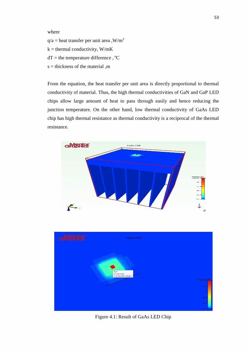
53
where
q/a = heat transfer per unit area ,W/m2
k = thermal conductivity, W/mK
dT = the temperature difference , oC
s = thickness of the material ,m
From the equation, the heat transfer per unit area is directly proportional to thermal
conductivity of material. Thus, the high thermal conductivities of GaN and GaP LED
chips allow large amount of heat to pass through easily and hence reducing the
junction temperature. On the other hand, low thermal conductivity of GaAs LED
chip has high thermal resistance as thermal conductivity is a reciprocal of the thermal
resistance.
Figure 4.1: Result of GaAs LED Chip

54
Figure 4.2: Result of GaP LED Chip
55
Figure 4.3: Result of GaN Chip
Table 4.1: Comparison of Result
Material
Thermal
Conductivity
(W/mK)
Junction
Temperature
(o C)
Color
GaAs 52 1230 Infrared (black)
GaP 110 266 Orange, Yellow,
Green
GaN 130 266 Blue

56
The high thermal resistance of the GaAs LED chip creates some pressure inside the
chip and causes heat cannot be conducted easily. As a result, more and more heat
accumulates inside the LED chip which leads to the increase of the junction
temperature. In this section, the author decided to use GaN LED chip to continue the
studies though GaN and GaP LED chips give the same junction temperature. GaN
LED chip is chosen as it is more stable and convenient in implementation compared
to GaP LED chip. Besides, GaN LED chip that generates blue light can be combined
with phosphor to create white light. LED chip that generates white light has a wide
range of application field as it gives high luminosity and cooler light. On the other
hand, GaP LED chip which can only produce yellow or green light is not suitable to
be used in many industry fields that require a bright working environment since
yellow light is a low lumen light.
4.1.2 Thermal Interface Material (TIM)
Next, the GaN LED module was added with a thin layer of TIM before it is attached
to the aluminum heat sink. Based on the experience in section 4.1.1, TC-5022 TIM
material was chosen as it has the highest thermal conductivity. The junction
temperature of the module is 271 oC which is 5 oC higher than the original GaN LED
module used in section 4.1.1. Table 4.2 tabulates the thermal conductivity of various
TIM materials, whereas Figure 4.4 shows the thermal distribution map of the module
that added with TIM layer.
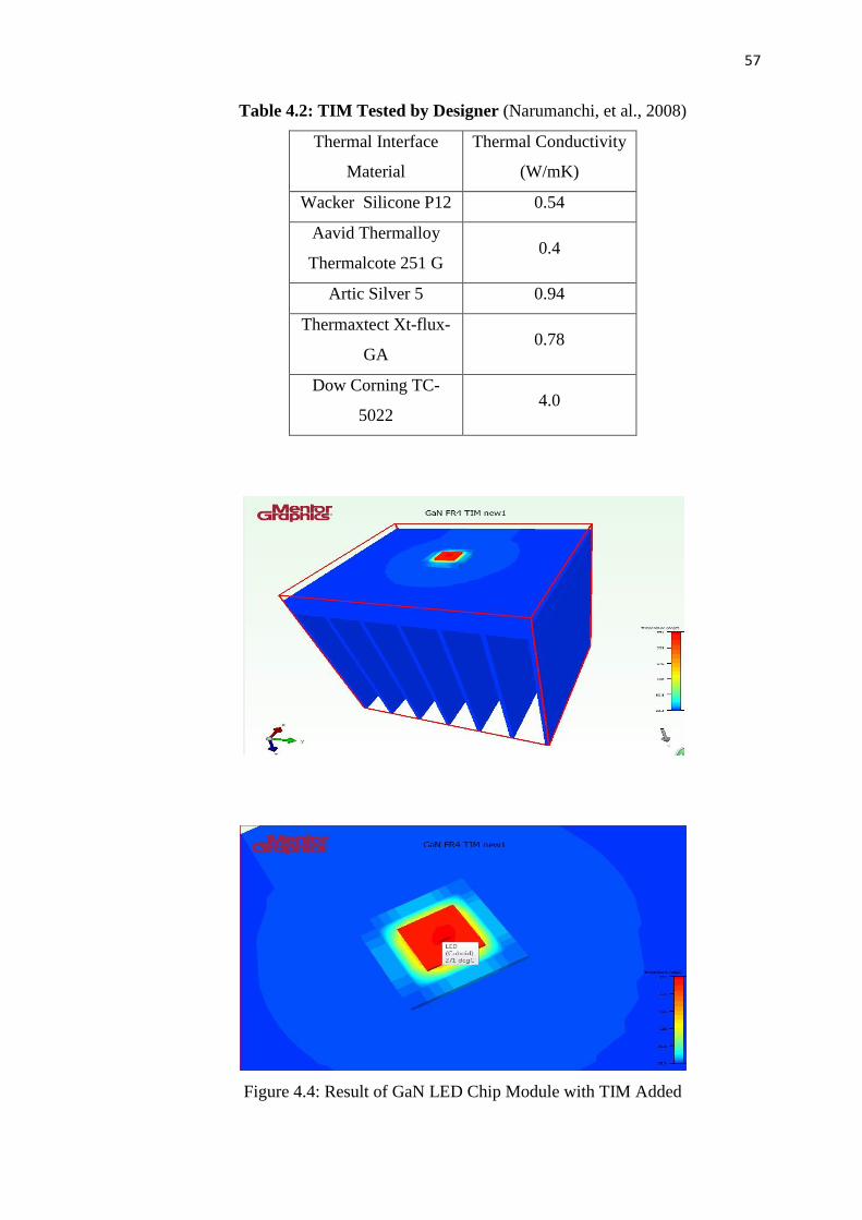
57
Table 4.2: TIM Tested by Designer (Narumanchi, et al., 2008)
Thermal Interface
Material
Thermal Conductivity
(W/mK)
Wacker Silicone P12 0.54
Aavid Thermalloy
Thermalcote 251 G 0.4
Artic Silver 5 0.94
Thermaxtect Xt-flux-
GA 0.78
Dow Corning TC-
5022 4.0
Figure 4.4: Result of GaN LED Chip Module with TIM Added

58
In real life, attaching the LED module to a heat sink require the surface of the LED
module and heat sink to be brought into intimate contact. These surfaces have a
twisted shape when observed in microscopic surface roughness viewed. As a result,
contact between the surfaces is not perfect and air gap formed between the surfaces
which cause a significant thermal resistance to the LED module. Thus, TIM material
is required to fill the air gap by covering the uneven surfaces. Yovanovich et al. have
calculated that using TIM grease to replace the air can reduced the thermal resistance
by factor of five depending on the surface and contact pressure. Because of using
TIM which has higher thermal conductivity than air to replace the air gap, the
thermal resistance between the surfaces has decreased and this greatly reduce the
junction temperature of the LED chip. Figure 4.5 shows the effect of apply the TIM
material.
Figure 4.5 Effect of Applying TIM
However, the LED module and the heat sink are in a perfect contact condition when
it is modeled by using CFD software. Adding a layer of TIM creates thermal
resistance between the surface due to its low thermal conductivity compared to the
thermal conductivity of the substrate and heat sink. However, there is only a mere
increase in the junction temperature since the TIM layer is very thin. Based on the
equation (4.1), the thin layer of TIM which is only 0.025 mm does not restrict the
Substrat
e Air Heat
sink
Before TIM applied, air
gap formed between
surfaces. Conduction
through contact point
and air
After TIM applied, air gap
is filled with TIM.
Conduction through TIM
TIM

59
conduction of heat seriously and the simulation result is still acceptable. Thus, the
author decided to add a layer of TIM while analyzing the LED modules so as to
mimic the structure of the real life LED module.
4.1.3 Thermal Conductivity of Substrate
The FR4 substrate (a material for printed circuit board) that used in the GaN LED
module was replaced with a copper MCPCB and DBC in order to study the thermal
performance of the module.
Figure 4.6: Result of GaN LED Module with MCPCB Substrate

60
Figure 4.7: Result of GaN LED Module with DBC substrate
The junction temperature of the GaN LED module with MCPCB substrate is 45.6 oC
and junction temperature of the GaN LED module with DBC substrate is 45 oC. The
results show that MCPCB and DBC are better material than FR4 substrate. This is
because MCPCB and DBC have a thermally conductive dielectric layer that has
relatively higher thermal conductivity than the FR4. The dielectric layer acts as a
good thermal bridge between the LED chips and the base copper plate. Besides, the
base copper plate can conduct the heat effectively to the heat sink to be dissipated to
the atmosphere. Besides of being thermal conductive, the dielectric layer has good
electric insulation that can help to prevent short circuit between the LED module and

61
heat sink. This helps increasing the stability of the LED module. The copper core,
which is a traditional PCB board on top of the dielectric layer, also helps to dissipate
some of the heat to the atmosphere directly. Eventually, it can reduce the junction
temperature of the LED chip. On the other hand, FR4 only can remove heat with the
use of heat sink. As a result, the thermal dissipation performance of the overall LED
module is poorer compared to LED module that has MCPCB or DBC substrate.
By comparing the thermal management performance of the MCPCB substrate
and DBC substrate, the author decided to use MCPCB though DBC has better
thermal management performance. This is because DBC has low thermal mechanical
reliability. It cracks easily in extreme temperature condition causing loss of isolation
properties. DBC also lack of flexibility in design to allow multiple copper
thicknesses and it cannot fabricate metalized via through ceramic substrate.
Therefore, MCPCB is chosen as it is more reliable and flexible in LED module
design (Person and Gundel, 2015).
4.2 LED Arrangement
In order to assess this criterion, multiple-chip LED module was generated through
the modeling software whereby the different orientations of the LED chips were thus
studied.
4.2.1 Number of LED Chips
Based on Table 4.3, an increase in number of LED chips yields an increment in
average junction temperature. The estimated thermal power loss of a single LED chip
is 2W. When the number of LED chips was increased by a factor of n, the estimated
thermal power loss increased by n too. This causes large amount of heat generated
around the LED chips. On the other hand, the heat sink used throughout this section
remains unchanged. When a module with eight LED chips was used, the heat sink
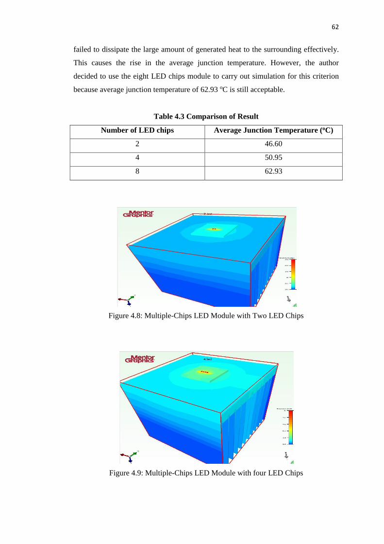
62
failed to dissipate the large amount of generated heat to the surrounding effectively.
This causes the rise in the average junction temperature. However, the author
decided to use the eight LED chips module to carry out simulation for this criterion
because average junction temperature of 62.93 oC is still acceptable.
Table 4.3 Comparison of Result
Number of LED chips Average Junction Temperature (oC)
2 46.60
4 50.95
8 62.93
Figure 4.8: Multiple-Chips LED Module with Two LED Chips
Figure 4.9: Multiple-Chips LED Module with four LED Chips

63
Figure 4.10: Multiple-Chips LED Module with eight LED Chips
4.2.2 Distance between the LED Chips
In this section, the eight LED chips module shown in Figure 4.10 has a distance of 2
mm between each LED chips. The module was further modified to have different
distance between the LED chips. Table 4.4 shows the simulation result of the LED
module with distance between LED chips of 2 mm, 4 mm, 6 mm and 8 mm.
Table 4.4: Comparison of Result
Distance between LED chips (mm) Average Junction Temperature (oC)
2 62.93
4 60.38
6 59.79
8 59.59
The results from Table 4.4 clearly show that a further distance between the LED
chips increases the average junction temperature. The temperature difference
between the multiple-chips LED module with distance between the LED chips of 8
mm and 2 mm is about 3 oC. When the gap between the LED chips is big, the heat

64
can be dissipated easily since there is less heat influence between the LED chips.
Besides, the outermost LED chips which are the first and the last LED chips always
have lower junction temperature compared to other LED chips. This is due to the fact
that there is more space for the first and the last LED chips to dissipate the heat. As a
result, more heat can be dissipated and this decreased the junction temperature.
Figure 4.11 shows that the first and last LED chips have larger area to dissipate the
heat when the distance between the LED chips is 2 mm. However, other designs
were not able to dissipate heat well due to heat influence. Figure 4.12 shows that all
the LED chips dissipate heat equally to all direction due to less heat influence.
Figure 4.11: Simulation Result of Multiple-Chips LED Module with Distance
between LED Chips of 2mm
Figure 4.12: Simulation Result of Multiple-Chips LED Module with Distance
between LED Chips of 8mm

65
4.2.3 Orientation of the LED Chips
Moreover, the eight chips LED module was modified to have different orientation of
the LED chips in rectangle orientation, triangle orientation, circle orientation and line
orientation. Figure 4.13, 4.14, 4.15 and 4.16 show the simulation result of the
modified eight chips LED chips module, respectively. Table 4.5 shows comparison
of the simulation results.
Figure 4.13: Simulation Result of Eight Multiple-Chips LED Module with Rectangle
Orientation
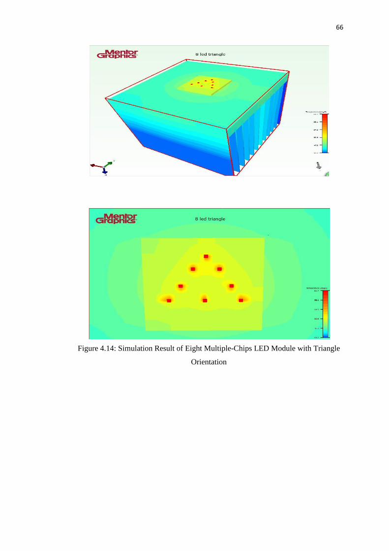
66
Figure 4.14: Simulation Result of Eight Multiple-Chips LED Module with Triangle
Orientation

67
Figure 4.15: Simulation Result of Eight Multiple-Chips LED Module with Circle
Orientation

68
Figure 4.16: Simulation Result of Eight Multiple-Chips LED Module with Straight
Line Orientation

69
Table 4.5 Comparison of result
Orientation Average junction temperature (oC)
Rectangle 61.64
Triangle 61.47
Circle 61.33
Line 59.59
Based on the results shown in Table 4.5, rectangle, triangle and circle orientation of
LED chips do not affect the thermal dissipation performance much and the average
junction temperature of the three multiple-chips LED module are almost same. Line
orientation allows the LED chips to dissipate the heat effectively and causes the
average junction temperature to be lower by 2 C compared to other orientations.
However, line orientation occupies more spaces compared to other orientation. If the
size of the substrate is a limiting factor, then circle orientation would be a good
alternative.
4.3 Heat Sink Design
In this section, the author designed a heat sink to study the parameters that can affect
the heat dissipation performance of the heat sink. The parameters studied include
heat sink area, heat sink thickness, fin height, fin width and number of fins. In the
studies for achieving optimum thermal performance, each parameter is independent
to each other. However in real life, these parameters maybe interdependent and it
may affect the overall thermal dissipation ability. Figure 4.17 shows the heat sink
used in present section and the average junction temperature of the LED chips are
137 C.

70
Figure 4.17: Heat Sink Used Before Modification
4.3.1 Area of Heat Sink
Figure 4.18: Result of LED Module with Area of 40 mm2
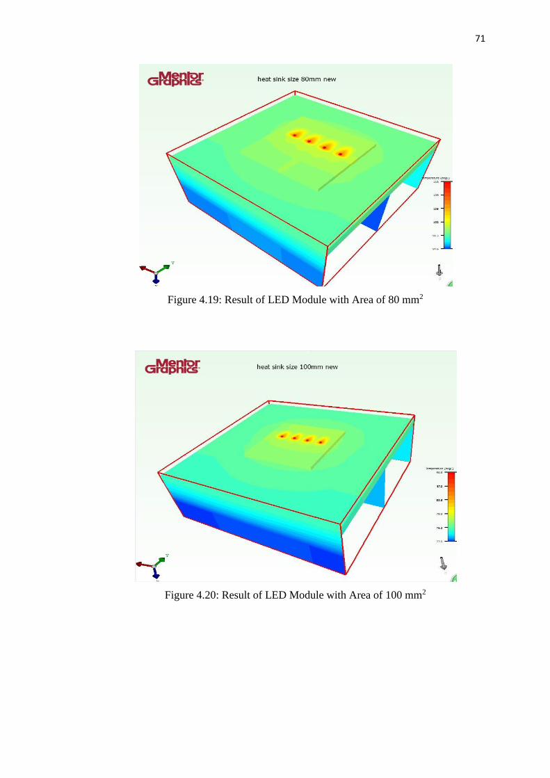
71
Figure 4.19: Result of LED Module with Area of 80 mm2
Figure 4.20: Result of LED Module with Area of 100 mm2
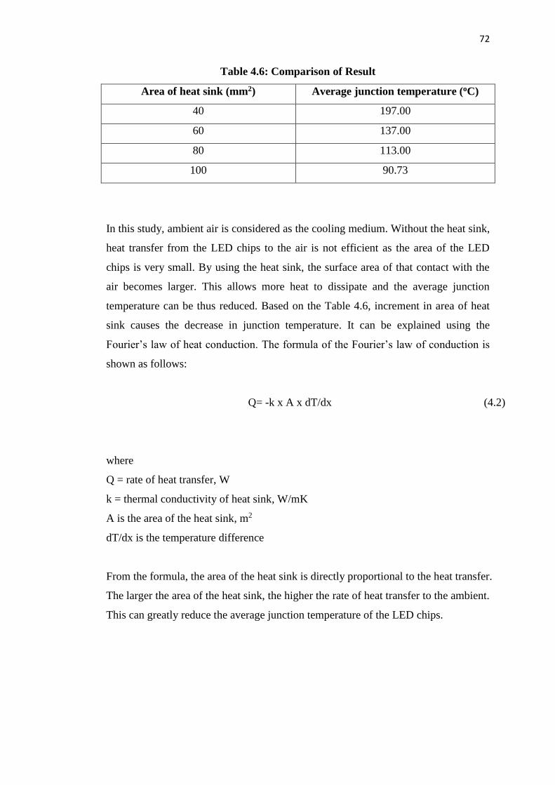
72
Table 4.6: Comparison of Result
Area of heat sink (mm2) Average junction temperature (oC)
40 197.00
60 137.00
80 113.00
100 90.73
In this study, ambient air is considered as the cooling medium. Without the heat sink,
heat transfer from the LED chips to the air is not efficient as the area of the LED
chips is very small. By using the heat sink, the surface area of that contact with the
air becomes larger. This allows more heat to dissipate and the average junction
temperature can be thus reduced. Based on the Table 4.6, increment in area of heat
sink causes the decrease in junction temperature. It can be explained using the
Fourier’s law of heat conduction. The formula of the Fourier’s law of conduction is
shown as follows:
Q= -k x A x dT/dx
(4.2)
where
Q = rate of heat transfer, W
k = thermal conductivity of heat sink, W/mK
A is the area of the heat sink, m2
dT/dx is the temperature difference
From the formula, the area of the heat sink is directly proportional to the heat transfer.
The larger the area of the heat sink, the higher the rate of heat transfer to the ambient.
This can greatly reduce the average junction temperature of the LED chips.

73
4.3.2 Thickness of Heat Sink
The heat sink thickness greatly affects the spreading resistance of the heat sink.
Spreading resistance occurs when the heat is transfer from a smaller area substance
to a larger area substance. In the heat sink, the spreading resistance causes the heat
cannot distribute evenly throughout the heat sink base which causes heat cannot be
transfer to each fins uniformly. As a result, there is a large temperature difference
between the centre of the heat sink and the edge of the heat sink (Advanced Thermal
Solution, 2007). From Table 4.7, increase in heat sink thickness causes decrease in
average junction temperature. It can also say that increase in the thickness of the heat
sink decreases the spread resistance of the heat sink.
Based on Figure 4.21, when the thickness is 0.1 mm, the spread resistance of
the heat sink becomes large. As a result, the heat cannot spread and all the heat can
only dissipate to the atmosphere through the fin that located at centre of the heat sink.
This implies that the heat sink is not fully utilized.
On the other hand, when the thickness of the heat sink was increased to 10
mm as shown in Figure 4.23, the temperature gradient between the centre of the heat
sink and edge of the heat sink became zero. This shows that the spread resistance is
reduced to the minimum value. The heat sink is fully utilized and the heat can spread
evenly through all the fins. Large amount of heat can be removed to atmosphere and
this reduces the junction temperature of the LED chips.
Table 4.7 Comparison of Result
Heat sink thickness (mm) Average junction temperature (oC)
0.1 151
1 138
10 133
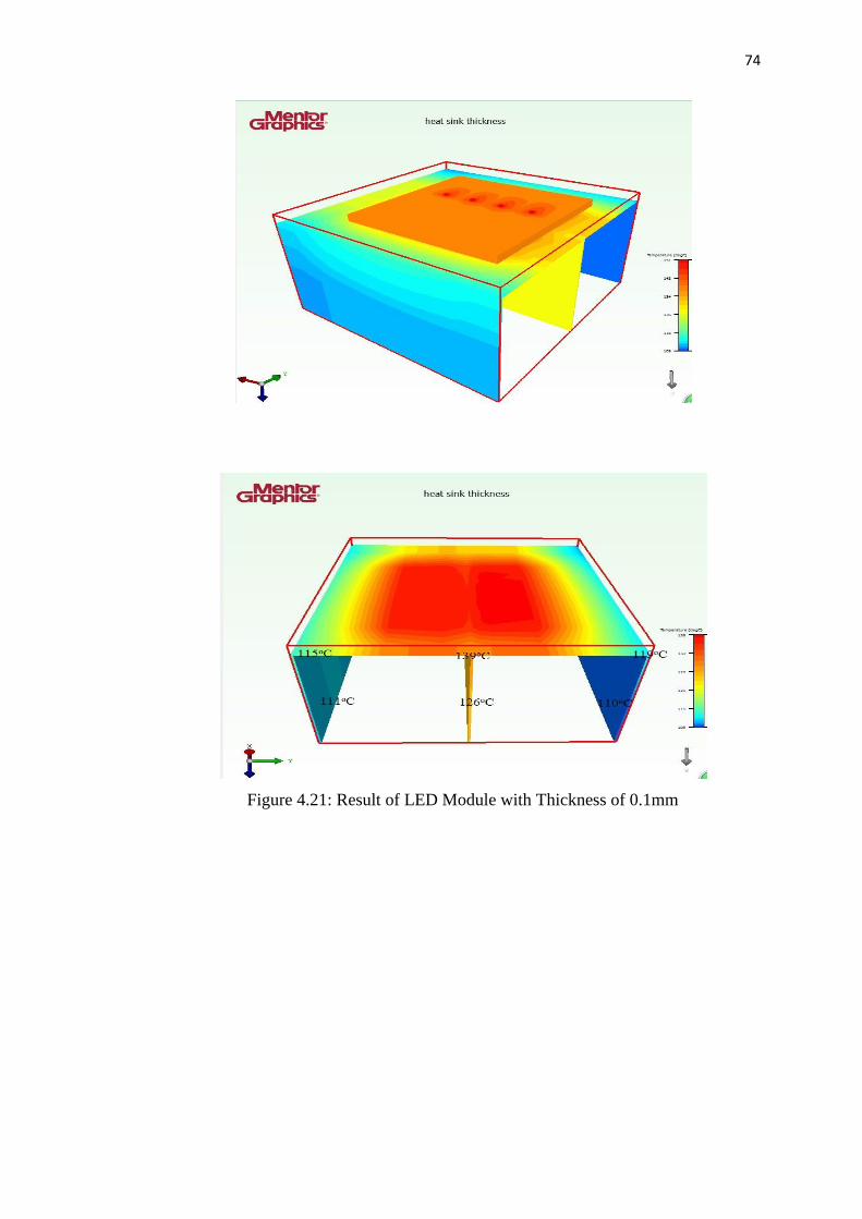
74
Figure 4.21: Result of LED Module with Thickness of 0.1mm

75
Figure 4.22: Result of LED Module with Thickness of 1mm

76
Figure 4.23: Result of LED Module with Thickness of 10mm
However, the heat sink cannot be designed to have the maximum thickness.
In fact, if the thickness exceeds the optimum thickness, the thermal resistance of the
heat sink would consequently increase. To explain it in a simple way, the heat cannot
transfer from base to the fins of the heat sink. The heat may accumulate at the base of
the heat sink and cause the rise in the average junction temperature.

77
4.3.3 Fin Height
Moreover, the heat sink was modified to have different fin heights. Table 4.8 shows
the comparison of three different heat sinks with fin height of 15 mm, 40 mm and 60
mm.
Table 4.8: Comparison of Result
Fin height (mm) Average junction temperature (oC)
15 161
40 126
60 112
Based on the result from Table 4.8, the heat sink which has longer fin height has
better heat dissipation performance. This is owing to the fact that longer fin height
provides additional contact area with the atmosphere that allows more heat to be
dissipated.
4.3.4 Fin Number
Increase in fin number causes increment in total convective surface area. Besides, it
also causes fin flow velocity decrease as a result of pressure drop. Based on Table
4.9, initially, increase in fin number increase the heat dissipation performance and of
the heat sink. This is because the gain from increase in surface area is greater than
loss in reduction of fin flow velocity. However, when the fin number exceeds the
optimum number which is 15 fins, increase in fin number causes decrease in heat
dissipation performance. Now, the lost due to reduce in fin flow velocity is greater
than gain from surface area. It can be said that the excessive fins block the air flow
and causes the hot air to stagnant between the fins. As a result, the heat cannot be
dissipated efficiently. The temperature gradient between the air and the fin is small
and conduction of heat cannot be carried out easily. Furthermore, the thermal
dissipation performance of 11 fins heat sink is almost the same as thermal dissipation

78
performance of the heat sink with optimum number of fin which is 15 fins. It is
recommended to use the heat sink with 11 fins because increase the number of fins to
15 is just adding the cost due to more material is needed but giving a result which is
almost the same as the heat sink of 11 fins. Besides, a different manufacturing
method is needed to produce the heat sink which has more than 11 fins. The
manufacturing method is time consuming and very expensive (Lee 1995).
Figure 4.24: Result of LED Module with 2 Fins
Figure 4.25: Result of LED Module with 4 Fins

79
Figure 4.26: Result of LED Module with 5 Fins
Figure 4.27: Result of LED Module with 11 Fins

80
Figure 4.28: Result of LED Module with 15 Fins
Figure 4.29: Result of LED Module with 16 Fins

81
Figure 4.30: Result of LED Module with 20 Fins
Figure 4.31: Result of LED Module with 22 Fins

82
Table 4.9: Comparison of Result
Fin number Average junction temperature (oC)
2 174
4 118
5 97.15
11 65.90
15 65.65
16 65.98
20 70.40
22 72.57
Figure 4.32: Graph Temperature Versus Fin Number
4.3.5 Fin width
Based on Table 4.10, increase in fin width beyond the optimum value which
is 7 mm causes increase in average junction temperature of the LED chips. It can be
explained as the case of increment the fin number beyond the optimum number.

83
Figure 4.33: Result of LED Module with Fin Width of 0.25mm
Figure 4.34: Result of LED Module with Fin Width of 1.5mm

84
Figure 4.35: Result of LED Module with Fin Width of 3mm
Figure 4.36: Result of LED Module with Fin Width of 6mm

85
Figure 4.37: Result of LED Module with Fin Width of 7mm
Figure 4.38: Result of LED Module with Fin Width of 8mm

86
Figure 4.39: Graph of Temperature Versus Fin Width
Table 4.10 Comparison of Result
Fin width (mm) Average junction temperature (oC)
0.25 138.00
1.5 132.75
3 129.00
6 125.00
7 124.50
8 128.00
4.3.6 Heat Sink with Hole
The original heat sink used is modified to have some venting hole at the base plate of
the heat sink. The dimension of the venting hole is 5 mm 5 mm.

87
Figure 4.40: Heat Sink with Venting Holes
Figure 4.41: Result of LED Module with Venting Holes

88
Figure 4.42: Velocity Map of the Heat Sink with Venting Holes
Figure 4.43: Velocity Map of the Original Heat Sink
The average temperature of the multiple-chip LED module with heat sink that has
venting hole is 102 C which is 35 C lower than the original heat sink. By
comparing the Figures 4.42 and 4.43, the maximum velocity of air flow of the heat

89
sink with ventilation hole is 0.229 ms-1 while the maximum velocity of the air flow
of the original heat sink is 0.148 ms-1. Moreover, there are more arrows on the
surface of heat sink shows in Figure 4.42, representing the air flows smoothly and
frequently than the air flows in Figure 4.43. The higher air flow rate ventilate heat
away effectively causes the efficient heat convection process and thus decrease in
average junction temperature of the LED chips. This confirms that heat sink with
ventilation hole is better since it provides good thermal management performance by
smoothing the air flow around the heat sink. It is also cost effective and less dense as
less material is required to manufacture it (Chu, Chang and Huang, 2015).
4.4 Optimization
After studying the factors that affect the thermal management performance of the
multiple-chips LED module, the author designed an optimized multiple-chips LED
module based on the analysis and experience of previous studies. The average
junction temperature of the four LED chips is 64.5 C which meets the requirement
set by manufacturer. Figure 4.44 shows the optimized multiple-chips LED module
designed and Figure 4.45 shows the thermal distribution map of the module. Table
4.11 shows the properties of the multiple-chips LED module.
Figure 4.44: Optimized Multiple-Chips LED Module
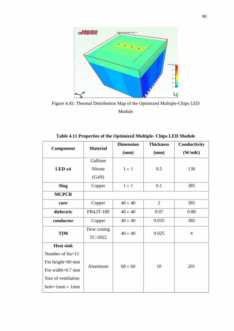
90
Figure 4.45: Thermal Distribution Map of the Optimized Multiple-Chips LED
Module
Table 4.11 Properties of the Optimized Multiple- Chips LED Module
Component Material Dimension
(mm)
Thickness
(mm)
Conductivity
(W/mK)
LED x4
Gallium
Nitrate
(GaN)
1 1 0.5 130
Slug Copper 1 1 0.1 385
MCPCB
core Copper 40 40 2 385
dielectric FR4,IT-180 40 40 0.07 0.88
conductor Copper 40 40 0.035 385
TIM Dow coning
TC-5022 40 40 0.025 4
Heat sink
Number of fin=11
Fin height=60 mm
Fin width=0.7 mm
Size of ventilation
hole=1mm 1mm
Aluminum 60 60 10 201

91
In the optimized module, GaN LED chips are selected due to their high
thermal conductivities and high luminous output. MCPCB substrate which has better
thermal dissipation performance is used to replace the original FR4 substrate.
Moreover, the heat sink used has optimized area for dissipate heat. With thickness of
10 mm, the spread resistance is minimized and the heat can spread evenly. From
Figure 4.45, the entire base of the heat sink is 52 C and represent in light green color.
This shows that the heat has spread evenly to every corner of the base of heat sink.
Moreover, the number of fin, fin height and wide are optimized to increase the total
surface area for the heat dissipation without reduce the air flow velocity. Ventilation
holes are also added to increase the air flow rate.
Figure 4.46: Optimized Multiple- Chips LED Module with Additional Heat Sink
Figure 4.47: Thermal Distribution Map of Optimized Multiple-Chips LED Module
with Additional Heat Sink

92
Table 4.12 Properties of the Optimized Multiple- Chips LED Module with
Additional Heat Sink
Component Material Dimension
(mm)
Thickness
(mm)
Conductivity
(W/mK)
LED x4 Gallium
Nitrate (GaN) 1 1 0.5 130
Slug Copper 50 1 0.1 385
MCPCB
core Copper 40 40 2 385
dielectric FR4,IT-180 40 40 0.07 0.88
conductor Copper 40 40 0.035 385
TIM Dow coning
TC-5022 40 40 0.025 4
Heat sink
Number of fin=11
Fin height=60mm
Fin width=0.7mm
Size of ventilation
hole=1mm 1mm
Aluminum 60 60 10 201
Additional heat
sink
Number of fin=5
Fin height=30mm
Fin width=2mm
Aluminum 15 40 5 201
Figure 4.46 shows two additional heat sinks are attached directly at the edge
of the copper slug. These two heat sinks are used to dissipate some of the heat that
conducts from the copper slug to the atmosphere directly. As a result, the thermal
dissipation ability of the multiple-chips LED module has improved and the average
junction temperature of the LED chips is 59.52 C. However, this design is not
recommended to the devices which emphases on mobility such as mobile phone and

93
laptop. This is because increase in number of heat sinks causes increase in the mass
and size of the module. Besides, total cost to manufacture the module also increase
too.

CHAPTER 5
CONCLUSION AND RECOMMENDATION
5.1 Conclusion
Multiple-chips LED module development and thermal management performance of
the chips were studied in this project. The main objectives of the project were
accomplished and concluded in this section. Besides, the recommendation and future
work are discussed in this chapter.
5.1.1 Development and Simulation of Multiple-Chips LED Module using
Computational Fluid Dynamic Software
Multiple-chips LED module was developed successfully using CFD software in this
project. It consists of LED chips, copper slug, substrate and heat sink. The LED
chips used throughout the project are 1 1 0.5 mm. The forward voltage across the
LED chips are 3V and the current flow through is 0.95 A. The thermal coefficient of
the chips is 70% and the calculated thermal power dissipation is 2 W. The copper
slug is used to attach the LED chips to the substrate. The substrate is a PCB board
containing the circuit to provide electric to the LED chips to light up and control the
brightness of the LED chips. Besides, it also provides mechanical support and helps
in heat dissipation. After that, the LED module is attached to a heat sink. The heat
sink plays an important role in thermal management performance of the multiple-
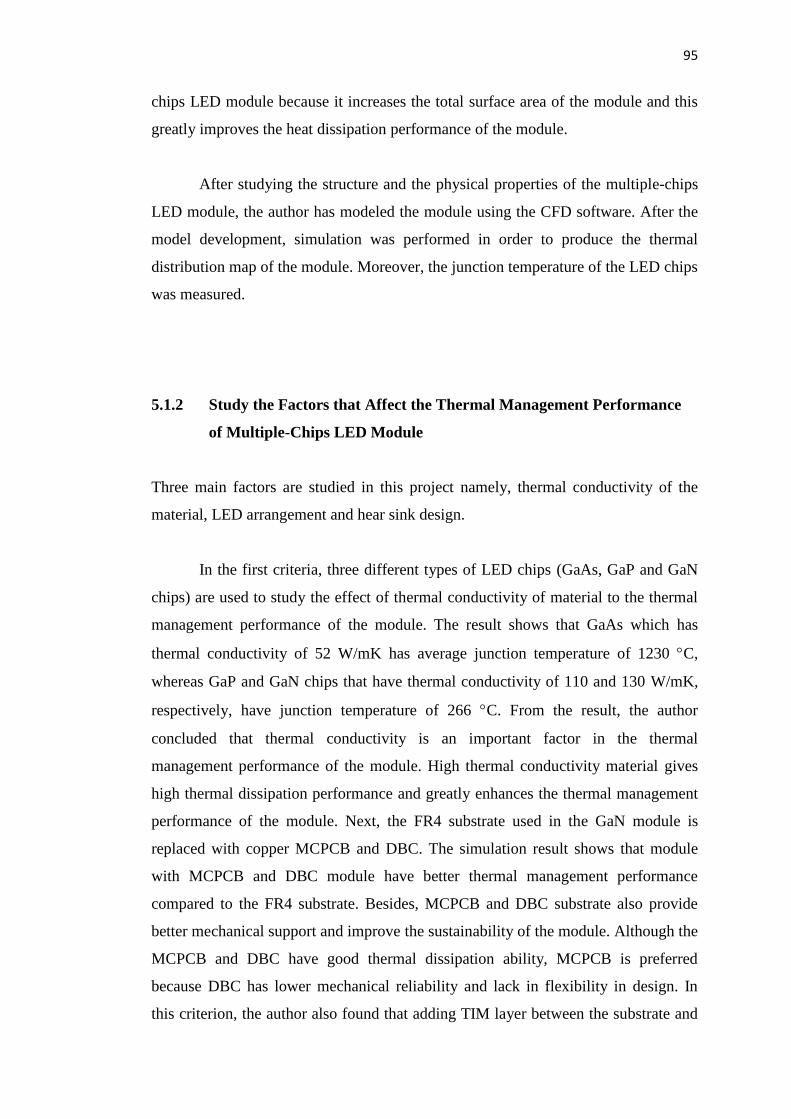
95
chips LED module because it increases the total surface area of the module and this
greatly improves the heat dissipation performance of the module.
After studying the structure and the physical properties of the multiple-chips
LED module, the author has modeled the module using the CFD software. After the
model development, simulation was performed in order to produce the thermal
distribution map of the module. Moreover, the junction temperature of the LED chips
was measured.
5.1.2 Study the Factors that Affect the Thermal Management Performance
of Multiple-Chips LED Module
Three main factors are studied in this project namely, thermal conductivity of the
material, LED arrangement and hear sink design.
In the first criteria, three different types of LED chips (GaAs, GaP and GaN
chips) are used to study the effect of thermal conductivity of material to the thermal
management performance of the module. The result shows that GaAs which has
thermal conductivity of 52 W/mK has average junction temperature of 1230 C,
whereas GaP and GaN chips that have thermal conductivity of 110 and 130 W/mK,
respectively, have junction temperature of 266 C. From the result, the author
concluded that thermal conductivity is an important factor in the thermal
management performance of the module. High thermal conductivity material gives
high thermal dissipation performance and greatly enhances the thermal management
performance of the module. Next, the FR4 substrate used in the GaN module is
replaced with copper MCPCB and DBC. The simulation result shows that module
with MCPCB and DBC module have better thermal management performance
compared to the FR4 substrate. Besides, MCPCB and DBC substrate also provide
better mechanical support and improve the sustainability of the module. Although the
MCPCB and DBC have good thermal dissipation ability, MCPCB is preferred
because DBC has lower mechanical reliability and lack in flexibility in design. In
this criterion, the author also found that adding TIM layer between the substrate and

96
heat sink does not improve the thermal management performance of the module.
This is because there is no air gap between the substrate and heat sink if the module
was developed using the software. Adding the TIM layer is just to increase the
thermal resistance between the substrate and the heat sink. However, the author
decided to use the TC-5022 which is a good TIM material that proven by other
designer in all the modules developed to make the modules operate like a real
module.
In addition, effect of number of LED chips and LED layout to the thermal
management performance of the module is studied. It is found that increase in the
number of LED chips will greatly increase the average junction temperature of the
LED chips. This is because the total thermal power loss increases with the increase in
number of the LED chips. As a result, the heat sink used fail to dissipate the large
amount of heat to the surrounding leading to increase in the average junction
temperature of the LED chips. Besides, the distance between the LED chips also
affects the thermal management performance of the module. The distance between
the LED chips must be wide enough to prevent heat influence between the LED
chips during the dissipation of heat. However, the distance between the LED chips
cannot be too wide because it will cause the size of the module increase. The author
found that 8 mm is the optimum distance because it can reduce the heat influence
between the LED while maintaining the overall small size of the module. Moreover,
different orientations of LED chips are studied so as to determine the orientation that
can improve the thermal management performance of the module. The straight line
and the circle orientation are better compared to triangle and rectangle orientation.
The author considered the straight line orientation is suitable as it gives the best
thermal management performance. If the size of the module is a limiting factor,
circle orientation can be chosen because it occupies less space although the thermal
management performance is poorer compared to the straight line orientation.
The last criterion involves the study of the heat sink design that affect the
thermal management performance of the multiple-chips LED module. Heat sink with
larger area and longer heat fin height is found to has better heat dissipation ability.
This is because large surface area and long fin height provide additional surface area
with the atmosphere which helps to dissipate heat to atmosphere easily. Next, the

97
thickness of the heat sink is also an important factor and it is related to the spreading
resistance of the heat sink. The thicker heat sink has low spreading resistance. When
the heat sink thickness is set to optimum value which is 10 mm, the spreading
resistance is very low and heat can spread evenly throughout the heat sink. The heat
sink is fully utilized and the thermal dissipation performance is improved. Beyond
the optimum thickness, the thermal resistance of the heat sink increases and causes
heat to accumulate at the base of heat sink. As a result, the heat cannot dissipate and
cause rise in junction temperature of the LED module. Moreover, increase in fin
number and fin width also improved the thermal dissipation performance of the
module because the total convection surface area of the heat sink has increased.
When the fin number and fin width exceed the optimum number, the excessive fins
and the fins are too thick to reduce the air flow around the fins. This causes hot air
stagnant around the fins and heat cannot be conducted from the heat sink to the air
easily. This greatly reduces the thermal dissipation performance of the heat sink. The
author decided to use 11 fins although the optimum number of heat sink is 15. This is
because the thermal dissipation performance of the heat sink with 11 fins and 15 fins
is almost the same. Heat sink with 11 fins is selected as heat sink with 15 fins
requires a different manufacturing method and the cost is very expensive compared
to heat sink that has 11 fins. Furthermore, heat sink with ventilation hole has high
thermal dissipation performance. The ventilation hole improved the air flow rate
around the fins of the heat sink. With higher air flow rate, more heat can be
ventilated through convection and this improves the thermal dissipation performance
of the heat sink.
5.1.3 Model a Multiple Chips LED Module that Has High Luminous Output
and Good Heat Dissipation Performance.
After studying the factors that affect the thermal management performance of the
LED module, optimized four LED chips module is developed. The GaN chips used
operate in 3V which gives high luminous output. Besides that, blue color light
generated by GaN can be combined with phosphor to generate white color light that
has high luminosity which suitable to be used in many industry fields that require

98
bright working environment. Copper MCPCB is used as substrate because it has
good thermal dissipation ability and can provide mechanical support to enhance the
sustainability of the module. The module is then attached to an optimized aluminum
heat sink. The heat sink has dimension of 60 mm 60 mm 10 mm. The heat sink
has 11 fins which have height of 60 mm and fin width of 0.7 mm. Moreover,
ventilation holes are added to improve the air flow rate around the fins. The average
junction temperature of the four LED chips is 64.5 C and it meets the requirement
set by manufacturer.
5.2 Recommendation and Future Work
This project has an extremely large potential to be improved in a few ways. The
optimized module has been developed successfully but many additional features can
be added to improve the thermal management performance of the module. All the
additional features are discussed in this section.
The main weakness of the optimized module is the size of the heat sink. The
6 cm2 heat sink is quite large and not suitable to be used in device that emphasis on
mobility. In order to reduce the size of the heat sink but also to maintain it good
thermal dissipation performance, thermal via can be introduced in the module. Figure
5.1 shows the implementation of the thermal via in a LED module. The thermal via
can reduce the thermal resistance of the module by providing an effective path for
the heat conduction from the LED chips to the heat sink directly.
Figure 5.1: LED Module with Thermal Via

99
Another method to improve the thermal management performance of the heat
sink is by introducing heat pipe. The heat pipe can be embedded in the base of the
heat sink to reduce the spreading resistance. As a result, the heat can distribute
evenly across the base of the heat sink base causing the base has high temperature.
Effective convection cooling can be achieved at the heat fins because more heat can
be conducted from the base to the heat fins due to larger temperature gradient
between the base and fins of the heat sink. Figure 5.2 shows two types of heat pipe
that can be embedded to the heat sink. With heat pipes added, the thickness and size
of the heat sink can be reduced while improving the thermal management
performance of heat sink.
Figure 5.2: Embedded and Surface Embedded Heat Pipe Heat Sinks
100
REFERENCES
Advanced Thermal Solution, Inc. 2007. Spreading thermal resistance; its definition
and control. Qpedia eMagazine, 50(2), pp. 49-52.
Altera, 2011. What is the difference between ambient temperature, junction
temperature, storage temperature and operating temperature? [online] Available
at < https://www.altera.com/support/support-resources/knowledge-
base/solutions/963.html> [ Accessed 14 Jun 2015]
Christenensen, A. and Graham, M. Ha, S. 2007. Thermal management method of
compact high power LED. Proc. of the SPIE, VOL 6669, Seventh International
Conference on solid state Lightning
Chu,L.M., Chang, W.C. and Huang, T.H. 2015. A Novel Heat Sink Design and
Prototyping for LED Desk Lamps. Mathematical Problems in Engineering.
Volume 2015, Article ID 765969, 8 pages.
Chuang, SL. (1997). Kinetic model of degradation of light emitting diode . IEEE
Journal of Quant Electronic VOL 3,NO 6,June 1997 pp.970-979
COFAN US, MCPCB construction. [online] Available at:< http://www.cofan-
usa.com/mcpcb-construction> [Accessed 5 January 2016]
DuPontTM CooLamTM , 2012. How substrate materials affect LED reliability. United
State: Lightning technology
Electrolube, 2015. Thermal management of LEDs : Looking Beyond Thermal
Conductivity Values. United kingdom: Electrolube
Jeong, MW., Jeon, SW., Lee, SH. and Kim,Y., 2015. Effective heat dissipation and
geometric optimization in an LED module with aluminum nitrate(AIN) insulate
plane. Applied Thermal Engineering ,76 (2015), pp. 212-219
Juntunen, E., Tapaninen, O., Sitomaniemi, A., Jamsa, M., Heikkinen, V., Karppinen,
M., and Karioja, P. 2014. Copper-Core MCPCB with Thermal Vias for High-
Power COB LED Modules. Power Electronics, IEEE Transactions on, 29(3), pp.
1410-1417.

101
Lee, S. 1995. Optimum design and selection of heat sinks. Semiconductor Thermal Measurement and Management Symposium, 1995. SEMI-THERM XI., Eleventh Annual IEEE,pp. 48-54. IEEE.
Ling, O., S., 2010. Thermal modeling of high power LEDs. Penang: Solid-State
Illumination Division, Avago Technologies
Liu, D., Yang, H. and Yang, P. 2014. Experimental and numerical approach on
junction temperature of high power LED. Microelectronic Reliability. 54 (2014),
pp. 926-931
Mentor Graphic . FLOTHERM article. United State: Mentor Graphic
M. Mohammad, M. Abdullah, M. Abdullah .2013. Experimental study on the cooling
performance of high power LED arrays under natural convection. Materials
Science and Engineering, 50,2013DOI: 10.1088/1757-899X/50/012030
Narumanchi, S., Mihalic, M., Kelly, K. and Eesley, G., 2008. Thermal interface
material for power electronic Application. In Thermal and Thermomechanical
Phenomena in Electronic Systems, 2008. ITHERM 2008. 11th Intersociety
Conference on (pp. 395- 404). IEEE.
Norton, T., Tiwari B., and Sun D.,W. 2013. Computational fluid dynamics in the
design and analysis of thermal processes: A review of recent advances. Critical
reviews in food science and nutrition 53.3 (2013), pp. 251-275.
OSRAM Opto Semiconductors, 2011. LED fundamentals: Internal thermal
resistance of LED. Penang: OSRAM
Person, R., and Gundel, P. 2015. Thick print copper technology increase thermal
reliability [online] Available at:
<http://www.electronicsprotectionmagazine.com/main/articles/thick-print-
copper- technology-increases-thermal-reliability/ > [Accessed 5 January 2016].
Poppe, A., Vass-Varnai, A., Farkas, G., and Rencz, M. 2008. Package
characterization: simulations or measurements?. Electronics Packaging
Technology Conference, 2008. EPTC 2008. 10th ,pp. 155-160.
Shi, D. , Feng, S. ,Zhang, Y., Qiao, Y. and Deng, B. 2015. Thermal investigation of
LED array with multiple packages based on the superposition method.
Microelectronic Journal ,46 (2015), pp.632-636
Stout, R., (2008) Psi or theta: which one should you choose?. Power Electronic
Technology, pp 20-24
102
The Engineering Toolbox. Thermal conductivity of material and gases. [online]
Available at: <http://www.engineeringtoolbox.com/thermal-conductivity-
d_429.html> [Accessed 7 January 2016].
Vakrilov, N., Andonova, A. and Kafadarova, N. Study of high power of COB LED
modules with respect to topology of chips. GaN (chips),130,150
XILINX, 2013. Packaging- Does XILIX provide " Theta-JB" ( thermal resistance
from junction to board) data for its packages? [online] Available at
<http://www.xilinx.com/support/answers/9088.html> [ Accessed 18 July 2015]
Yang, KS., Chung, CH., Lee, MT., Chiang, SB., Wong, CC and Wang, CC.,2013.
An experimental study on the heat dissipation of LED lighting module using
metal/carbon foam. International Communications in Heat and Mass Transfer, 48
(2013) , pp.73-79
Yin, L., Yang, L., Yang, W.,G.Y., Mac, K., Li S. and Zhang J.,2010. Thermal design
and analysis of multi-chip LED module with ceramic substrate, Solid-State
Electronic, Vol.54,2010, pp. 1520-1524
Yovanovich, M. M., Culham, J. R., and Teertstra, P., 1997. Calculating Interface
Resistance, ElectronicsCooling, 3(2), pp. 24 – 29.