Embed Size (px)
Citation preview
THERMIONIC-FIELD EMISSION
IN AIGaAs/GaAs 1WO-DIMENSIONAL ELECTRON GAS CHARGE-COUPLED DEVICES
J.-1. Song, D.V. Rossi, S. Xin, W.1. Wang, and E.R. Fossum
Department of Electrical Engineering
Columbia University
New York, NY 10027
ABSTRACT
Dark current in AIGaAs/GaAs two-dimensional electron gas charge-coupled devices
(2DEG CCDs) is investigated both theoretically and experimentally. Measurement of the
dark current for temperatures in the range 160 K to 360 K was performed and compared
with the results of numerical modelling. It is found that thermionic-field emission of
electrons from the gate to the channel is the dominant mechanism in uniformly-doped and
planar-doped device structures. Good agreement between theory and experiment was
obtained.
Metal-semiconductor field-effect transistor (MESFET)-type GaAs charge-coupled
devices (GGOs) have demonstrated high charge transfer efficiency (GTE) at frequencies
exceeding 1 GHz and are applicable to very high speed analog signal processing'. With
the advent of new infrared detectors built from III-V materials by molecular beam epitaxy
(MBE) or metal-organic chemical vapor deposition (MOCVOl, the potential integrability
of the detector and III-V based CCOs has motivated the investigation of GaAs and related
heterostructure GCOs for monolithic imaging detector array readout applications. Two
dimensional electron gas (20EG) CCDs, an emerging technology, are expected to have
several advantages over MESFET-type GaAs CCDs: a higher electron mobility at low
electric field and temperature, a larger charge handling capacity, a low insertion loss, a
reduced clock swing, and a fabrication compatibility with high speed, low noise 2DEG
field-effect transistors (FETs) for output amplifiers and supporting digital circuitry.
Recently, the first resistive-gate (20EG) CGD on a uniform-doped
Alo3Gao.7As/GaAs heterostructure was reported3, and demonstrated high charge transfer
efficiency (CTE of 0.9990) for clock frequencies between 13 MHz and 1 GHz at room
temperature. Degradation of CTE and reduction of the output signal amplitude were
observed for lower frequencies (for example, CTE of 0.98 at 1.5 MHz clock frequency),
due to the anomalous accumulation of carriers in the CCO well, referred to as dark
current. A thermally activated gate leakage current was believed to be the origin of the
dark current since the CTE was improved by cooling the device and subsequent
measurement of the gate leakage current showed that the total accumulation of the gate
leakage current in the CCO potential well during the period of charge transfer was
consistent with the maximum well capacity.
2
Extension of the low frequency operating range of the 20EG CCO , which is directly
related to the dark current, is important for infrared imaging detector array readout
applications to allow long integration periods at low temperature, nominally 65 K. An
understanding and reduction of dark current is also important for 2DEG-based dynamic
memory devices and circuits. In this paper, reduction of the gate leakage current by more
than two orders of magnitude through the use of a planar-doped structure is reported.
The physical mechanism responsible for the dark current is shown to be thermionic field
emission.
The material structure of the 2DEG CCO consists of, from bottom to top, a
semi-insulating GaAs substrate, a GaAs/AIGaAs superlattice buffer, an 8000 A thick
undoped GaAs layer, a 30 A thick undoped AIGaAs spacer layer, a planar-doped AIGaAs
layer (4.5x10 12 Si atoms/cm\ a 350 A thick undoped AIGaAs layer, and a 300 A thick
GaAs cap layer doped with 4x10¹⁸/cm 3 Si atoms. After a 4000 A deep mesa etch, AuGe
ohmic contacts were formed and annealed at 425 C for 45 sec under a forming gas am
bient. Using the AuGe ohmic pattern as a mask, the 300 A GaAs cap layer and 100 A of
the AIGaAs layer were etched with a 1:1 :1000, NH 40H:H 20 2 :H 20 solution. A resistive layer
(cermet) was e-beam evaporated on the CCO channel with an equal weight mixture of Cr
and SiO powder sources4, forming a Schottky contact to the underlying AIGaAs layer. The
resistive layer was 3000 A thick with a sheet resistance of 250 kn/o. The first Cr and Au
metallization was done bye-beam and thermal evaporations, respectively, to form finger
electrodes on the resistive layer and gate electrodes for the output amplifier. The second
Cr/ Au metallization was used to connect finger electrodes with the same phase (using a
3500A thick SiD as an inter-layer dielectric).
The CCO delay line is composed of 32 stages with a four-phase clocking scheme
3
(128 electrodes). The finger electrodes are 1pm long, 100 pm wide and spaced by 4 pm.
A source-follower (1 pm long, 100 pm wide gate) with the same size on-chip load and a
dual-gate reset FEr were used to read out the signal from the CCO channel.
Before operating the CCO delay line, basic device characterization was performed.
The pinch-off voltage and transconductance of a 1 pm gate FEr were
-1 V and 100 mS/rnm, respectively. The gate leakage current of the planar-doped
structure was measured to be more than two orders of magnitUde lower than that of a
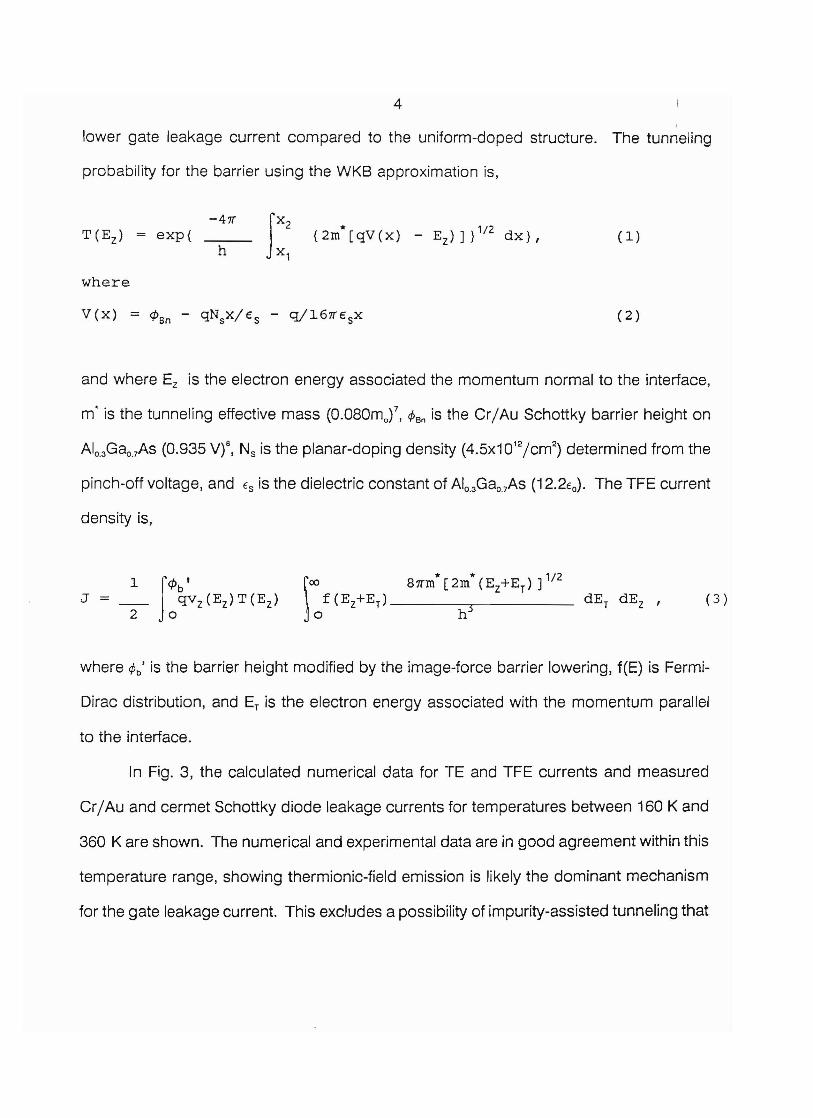
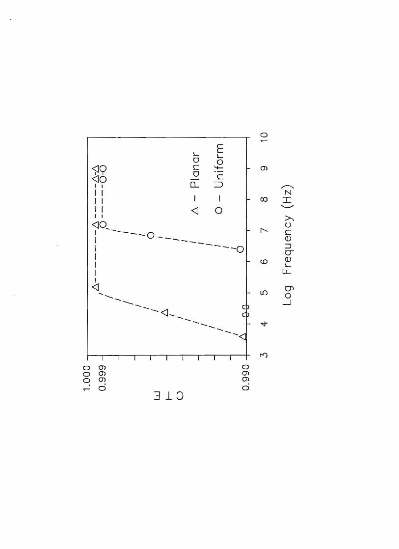
uniform-doped structure at room temperature. The CTE of this device is plotted in
Fig. 1 in comparison with that of the uniform-doped ceo, which shows an extended low
frequency limit by a similar factor as the gate leakage reduction. (Note that the test
station limit was 1GHz.) The eTE was evaluated using the method of Brodersen, et a1. 5.
To understand the low frequency limit of this device, various mechanisms of gate
leakage current were considered and analyzed. It should be noted that in the depletion
mode CCO, electron transport from gate to channel is of concern, whereas in typical
enhancement-mode 20EG FETs, transport from channel to gate dominates gate leakage
current. Calculation of thermionic emission (TE) current predicted current levels much
lower than experimentally seen, so that other mechanisms such as thermionic-field
emission (TFE)6 or impurity-assisted tunneling were considered. In order to resolve the
mechanisms, a numerical calculation was performed to calculate the TFE current. Since
the gate leakage current of the eco channel reaches a saturated maximum when the
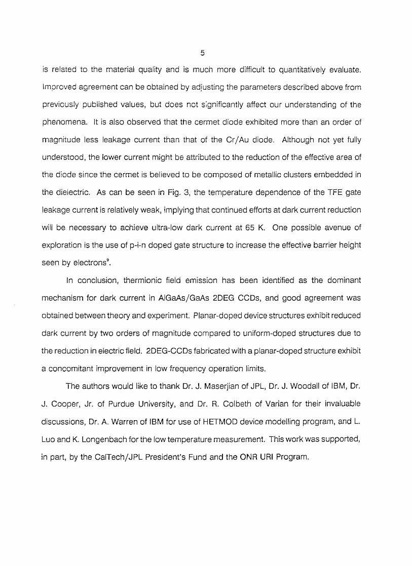
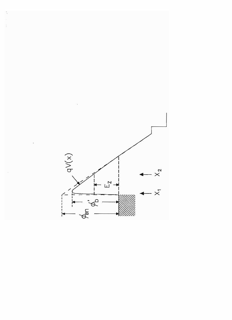
potential well is empty of signal charge, the modelled structure was assumed to be
reverse-biased beyond the pinch-off voltage with the barrier shape shown in Fig. 2. The
effective barrier is reduced by increased surface electric field leading to a qualitative
understanding as to why the planar-doped structure, with lower surface electric field, has
--
4
lower gate leakage current compared to the uniform-doped structure. The tunneling
probability for the barrier using the WKB approximation is,
-41T T(Ez) = exp{
h (1)
where
(2)
and where Ez is the electron energy associated the momentum normal to the interface,
m' is the tunneling effective mass (O.OaGmor, rPan is the Cr/ Au Schottky barrier height on
AI0.3GClo.7As (0.935 V)8, Ns is the planar-doping density (4.5x10¹²/cm2) determined from the
pinch-off voltage, and Es is the dielectric constant of AI0.3Gao.As (12.21:0), The TFE current
density is,
81Tm*[2m*(E +E ) ]1/21 z r J = ( 3 )
h 32
where rPb' is the barrier height modified by the image-force barrier lowering, f(E) is Fermi
Dirac distribution, and ET is the electron energy associated with the momentum parallel
to the interface.
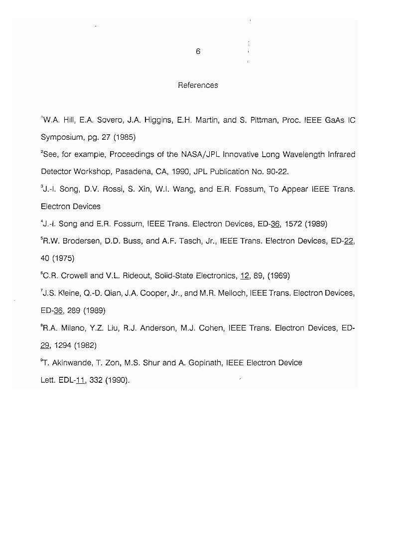
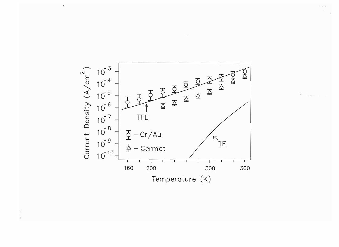
In Fig. 3, the calculated numerical data for TE and TFE currents and measured
Cr/ Au and cermet Schottky diode leakage currents for temperatures between 160 K and
360 K are shown. The numerical and experimental data are in good agreement within this
temperature range, showing thermionic-field emission is likely the dominant mechanism
for the gate leakage current. This excludes a possibility of impurity-assisted tunneling that
5
is related to the material quality and is much more difficult to quantitatively evaluate.
Improved agreement can be obtained by adjusting the parameters described above from
previously published values, but does not significantly affect our understanding of the
phenomena. It is also observed that the cermet diode exhibited more than an order of
magnitude less leakage current than that of the Cr/ Au diode. Although not yet fully
understood, the lower current might be attributed to the reduction of the effective area of
the diode since the cermet is believed to be composed of metallic clusters embedded in
the dielectric. As can be seen in Fig. 3, the temperature dependence of the TFE gate
leakage current is relatively weak, implying that continued efforts at dark current reduction
will be necessary to achieve ultra-low dark current at 65 K. One possible avenue of
exploration is the use of p-i-n doped gate structure to increase the effective barrier height
seen by electrons9•
In conclusion, thermionic field emission has been identified as the dominant
mechanism for dark current in AIGaAs/GaAs 20EG CCOs, and good agreement was
obtained between theory and experiment. Planar-doped device structures exhibit reduced
dark current by two orders of magnitude compared to uniform-doped structures due to
the reduction in electric field. 20EG-CCOs fabricated with a planar-doped structure exhibit
a concomitant improvement in low frequency operation limits.
The authors would like to thank Dr. J. Maserjian of JPL, Dr. J. Woodall of IBM, Dr.
J. Cooper, Jr. of Purdue University, and Dr. R. Colbeth of Varian for their invaluable
discussions, Dr. A. Warren of IBM for use of HETMOD device modelling program, and L.
Luo and K. Longenbach for the low temperature measurement. This work was supported,
in part, by the CaITech/JPL President's Fund and the ONR URI Program.
6
References
'W.A. Hill, E.A Sovero, J.A Higgins, E.H. Martin, and S. Pittman, Proc. IEEE GaAs IC
Symposium, pg. 27 (1985)
2See, for example, Proceedings of the NASAj,JPL Innovative Long Wavelength Infrared
Detector Workshop, Pasadena, CA, 1990, JPL Publication No. 90-22.
3J._1. Song, D.V. Rossi, S. Xin, W.1. Wang, and E.R. Fossum, To Appear IEEE Trans.
Electron Devices
4J._1. Song and E.R. Fossum, IEEE Trans. Electron Devices, ED-36, 1572 (1989)
5R.W. Brodersen, D.O. Buss, and AF. Tasch, Jr., IEEE Trans. Electron Devices, ED-22,
40 (1975)
6C.R. Crowell and V.L. Rideout, Solid-State Electronics, .12, 89, (1969)
7J.S. Kleine, O.-D. Oian, J.A Cooper, Jr., and M.R. Melloch, IEEE Trans. Electron Devices,
ED-36, 289 (1989)
BR.A Milano, Y.Z. Liu, R.J. Anderson, M.J. Cohen, IEEE Trans. Electron Devices, ED
29, 1294 (1982)
~. Akinwande, T. Zon, M.S. Shur and A Gopinath, IEEE Electron Device
Lett. EDL-l1, 332 (1990).
7
Figure Captions
Fig. 1 Frequency dependence of charge transfer efficiency (CTE) for the resistive-gate
planar-doped AIGaAs/GaAs 20EG CCO (1 GHz clock frequency is the limit of our
test station).
Fig. 2 Energy band diagram of a reverse-biased Schottky diode on a planar-doped
AIGaAs/GaAs heterostructure used for the numerical model.
Fig. 3 Gate leakage current of the planar-doped AIGaAs/GaAs heterostructure as a
function of temperature. Symbols are experimental data points and solid line
shows results of thermionic-field emission and thermionic emission calculations.
-----
o
l.- E I.
0 0 c '+- 0>~9 0 c<]0 I I Q.. :::::::> I I
I II I I I <] 0 I I
I I I I
,I<]
..... ......... _'
---<3 ........ -....-....."
o 0> o 0> o 0> ~ 0
o 0> 0> o
31J
N X
...... x
"...........,.
C'J 10- 3 E 0 10- 4
« ""'-../ 10- 5
.-~
+-' 10- 6 (f)
c 10- 7 (1)
0 10- 8
-+-I
(1) c
10- 9 L L :::J 10- 10
~ ~
7\ ~
~ -0
160 200 300 360
Temperature (K)
~ ~
2 -Cr/Au
Cermet

![Conduction Model for Semiconductor-Grain- Boundary ... · For example, in films with a grain size of 200 a [3], the ratio thermionic-field-emission component to thermionic-emission](https://img.pdfslide.net/doc/110x75/5e1d951a0415a662393e0226/conduction-model-for-semiconductor-grain-boundary-for-example-in-films-with.jpg)


![Instability due to trapped electrons in magnetized multi ... · charging mechanisms [11], namely thermionic emission, field emission, radioactivity, impact ionization, etc. These](https://img.pdfslide.net/doc/110x75/5f8d6fa4698d2313b81b15ba/instability-due-to-trapped-electrons-in-magnetized-multi-charging-mechanisms.jpg)


![THERMIONIC EMISSION FROM OXIDE-COATED - [email protected]](https://img.pdfslide.net/doc/110x75/62062d978c2f7b1730052693/thermionic-emission-from-oxide-coated-emailprotected.jpg)