Embed Size (px)
Citation preview

Page 1 of 21
Keywords: thermoelectric cooler, TEC, optical microcontroller, laser, thermal-loop, current-loop, dual loop control, digital signal processing, DSP, H-bridge, PWM, ADC, DAC, C discrete time, z-transform APPLICATION NOTE 5425
Thermoelectric Cooler Control Using the DS4830A Optical Microcontroller © Feb 10, 2015, Maxim Integrated Products, Inc. Abstract: This application note first briefly discusses the basic operation theory of a thermoelectric cooler (TEC) and its application in optical modules. Then it presents a digital approach to TEC control based on the DS4830A optical microcontroller. Mathematical analysis, algorithm implementation, firmware flowcharts, coding tips as well as an example code are included to make this article a step-by-step guide for TEC control using the DS4830A. Accuracy of ±0.1°C is readily achievable with TEC devices used in typical optical modules. Introduction This article begins with a brief discussion of the basic operational theory of a thermoelectric cooler (TEC) and its application in optical modules. It then presents a digital approach for TEC control that uses an optical microcontroller. Mathematical analysis, algorithm implementation, firmware flowcharts, coding tips, and an example code are included to make this article a step-by-step guide for TEC control. The appendices include a digital filter coefficient calculator lab results and an example code. Part I : Background Information Principle of Operation for a TEC A thermoelectric cooler (TEC) is a device based on the Peltier effect. It typically comprises two kinds of materials and transfers heat from one side of the device to the other while a DC current is forced through it. The side from which heat is removed becomes cold; the side to which heat is moved becomes hot. When the current reverses its direction, the previously “cold” side becomes hot and the previously “hot” side becomes cold. A TEC has no moving parts or working fluids, so it is very reliable and can be very small in size. TECs are used in many applications that require precision temperature control, including optical modules. There are two main reasons why an optical module may need precision temperature control.
1) The laser needs to be cooled or heated to maintain its optical performance. 2) The laser needs to be set at a specific wavelength.
Page 2 of 21
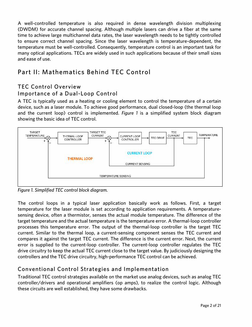
A well-controlled temperature is also required in dense wavelength division multiplexing (DWDM) for accurate channel spacing. Although multiple lasers can drive a fiber at the same time to achieve large multichannel data rates, the laser wavelength needs to be tightly controlled to ensure correct channel spacing. Since the laser wavelength is temperature-dependent, the temperature must be well-controlled. Consequently, temperature control is an important task for many optical applications. TECs are widely used in such applications because of their small sizes and ease of use. Part I I : Mathematics Behind TEC Control TEC Control Overview Importance of a Dual-Loop Control A TEC is typically used as a heating or cooling element to control the temperature of a certain device, such as a laser module. To achieve good performance, dual closed-loop (the thermal loop and the current loop) control is implemented. Figure 1 is a simplified system block diagram showing the basic idea of TEC control.
Figure 1. Simplified TEC control block diagram. The control loops in a typical laser application basically work as follows. First, a target temperature for the laser module is set according to application requirements. A temperature-sensing device, often a thermistor, senses the actual module temperature. The difference of the target temperature and the actual temperature is the temperature error. A thermal-loop controller processes this temperature error. The output of the thermal-loop controller is the target TEC current. Similar to the thermal loop, a current-sensing component senses the TEC current and compares it against the target TEC current. The difference is the current error. Next, the current error is supplied to the current-loop controller. The current-loop controller regulates the TEC drive circuitry to keep the actual TEC current close to the target value. By judiciously designing the controllers and the TEC drive circuitry, high-performance TEC control can be achieved. Conventional Control Strategies and Implementation Traditional TEC control strategies available on the market use analog devices, such as analog TEC controller/drivers and operational amplifiers (op amps), to realize the control logic. Although these circuits are well established, they have some drawbacks.

Page 3 of 21
1) The analog implementation usually requires many components, which in turn requires more PCB area. Having more components also renders higher failure rates.
2) In analog approaches, the control thresholds and coefficients are set by discrete
components. To achieve high control performance, components with tight tolerances need to be used which, in turn, increases cost. These components are also subject to drift over time which can affect TEC performance.
3) From a development point of view, it is not easy to modify a developed circuit to work for a
new application. The component values are interdependent and one must change a number of components to make a modification.
Digital TEC Control Using the DS4830A Optical Controller The DS4830A is a 16-bit low-power microcontroller with the necessary resources to make high-performance digital TEC control possible. The microcontroller needs to have several integrated capabilities:
• 13-bit analog-to-digital converter (ADC) with 26-input mux • Eight-channel independent 12-bit digital-to-analog converter (DAC) • 10 pulse-width modulation (PWM) channels with up to 16-bit resolution • 32k words of flash memory and 2k words of SRAM • Single-cycle multiply-accumulate unit (MAC) with a 48-bit accumulator
Unlike analog TEC controllers, the DS4830A optical microcontroller implements the control logic using digital signal processing (DSP) with firmware. This reduces the number of components needed and also makes the control parameters more accurate and repeatable. In addition, it is easier to modify firmware to accommodate new applications than to change discrete components. Figure 2 is a system block diagram that illustrates the digital TEC control approach.
Figure 2. DS4830A TEC control block diagram. There are some important observations to make from this TEC control approach:
Page 4 of 21
1) Temperature is converted to and represented by a voltage. Controlling the thermistor voltage is virtually controlling the laser module’s temperature.
2) All the input signals are digitized before being processed. The set-point voltage and the
thermistor voltage are converted using single-ended channels; the TEC current and voltage are converted using differential channels for better performance.
3) Both the thermal-loop controller and the current-loop controller in Figure 2 are
implemented digitally, which reduces the number of components used.
4) The thermal loop and current loop have different update periods. The thermal-loop update period is usually a multiple of the current-loop update period. This will be discussed in more detail later.
In the next section, we will discuss the principle and operation of the thermal-loop controller. DS4830A TEC Control: Operation of the Thermal Loop The main function of the thermal-loop controller is to process the temperature error, i.e., the difference of the target temperature and the actual temperature of the laser module, and generate a target TEC current. This is illustrated in Figure 1. More detail on this is shown in Figure 2. As explained earlier, temperature is converted to and represented by a voltage. In particular, the target temperature of the laser module is represented by the set-point voltage, which is denoted by VSET. The thermistor is typically placed very close to the laser module so that the temperature of the thermistor is virtually the same as that of the laser module. Again, the thermistor temperature is represented by the voltage across the thermistor, VTHERM. Controlling the temperature of the laser module is equivalent to controlling VTHERM. Since the thermal-loop controller is digitally implemented, both the set-point voltage and the thermistor voltage are digitized by ADC. Analog Prototype for the Thermal-Loop Controller A pragmatic way of developing a digital controller is to find the digital equivalent of a working analog controller. There are many analog control circuits available for TEC control applications, and Figure 3 is one of them. The circuit in Figure 3 takes VSET and VTHERM and generates VCTLI. The circuit is a proportional integral derivative (PID) controller. Its principle of operation is detailed in application note 3318, “HFAN-08.2.0: How to Control and Compensate a Thermoelectric Cooler (TEC).” The strategy here is to first find the continuous time transfer function of the circuit in Figure 3 and then converting the transfer function to the discrete time.

Page 5 of 21
Figure 3. An analog PID controller circuit. Based on the circuit shown in Figure 3, VCTLI can be expressed in terms of VSET and VTHERM. Since complex impedances are involved, it is convenient to introduce the complex variable s = j(2πf) =
jω. Thus, the impedance of a capacitor C1 is 11sC
. Taking advantage of basic op amp properties
and some algebraic manipulations, we have the expression for VCTLI in s-domain as follows:
)()()()()( svsGsvsGsv setFerrCCTLI += (Eq. 1)
Where: )()()( svsvsv thermseterr −= (Eq. 2)
1)111(2)331)(32(
)11121)(231()( −+++
+++−=
CsRRCsRCCsCsRCsRCsRsGC (Eq. 3)
1)111)(331)(32(
)231(1)( ++++
+=
CsRCsRCCCsRCsGF (Eq. 4)
Define:
)()()(1 svsGsv errC= (Eq. 5)
)()()(2 svsGsv setF= (Eq. 6) We can then rewrite )(svCTLI as:
)()()( 21 svsvsvCTLI += (Eq. 7)
Now CTLIV (s)can be seen as the sum of the outputs of two single-input single-output (SISO) systems. Each system can be characterized by its transfer function, i.e., )(sGC and )(sGF , respectively. The strategy here is to convert these two continuous time transfer functions to ther
set
therm
CTLI
C1 R1 C3
R3R2
THERMISTOR
C2
Page 6 of 21
discrete time, so they can be implemented by firmware. We use )(zGC and )(zGF to denote the discrete time domain equivalent of )(sGC and )(sGF , respectively. This idea is illustrated in Figure 2. Bi l inear Transformation There are several ways to convert analog systems to digital. Among them, bilinear transformation is widely used due to its property of preserving stability. The bilinear transformation is a stability preserving mapping from the continuous domain to the discrete domain. In the following discussions, the time interval is denoted by the sampling interval T (in seconds). The bilinear transformation is implemented by a change of variables which transforms on an s-domain transfer function to a z-domain transfer function. The usual form is:
112
+−
=zz
Ts (Eq. 8)
The z-transform transfer functions of the digital filters )(zGC and )(zGF are obtained from the corresponding s-domain transfer functions )(sGC and )(sGF by substituting for s the bilinear form of Equation 8, respectively. Obtaining Difference Equations for ][1 nv and ][2 nv We obtain the analytical expressions for )(zGC and )(zGF by plugging Equation 8 into Equations 3 and 4, respectively. This is a straightforward process, but it requires numerous algebraic operations. Their final analytical expressions in terms of R-C values are given in Appendix A. Finally, after inverse z-transform, discrete time signals ][1 nv and ][2 nv are obtained as shown below.
∑∑==
−+−−=3
0
3
111 ][_][][
jj
ii jnerrvBinvAnv (Eq. 9)
∑∑==
−+−−=2
0
2
122 ][_][][
ll
kk lnsetvDknvCnv (Eq. 10)
Since this is a linear system, the superimposition property applies. We have:
][][][_ 21 nvnvnCTLIv += (Eq. 11) The coefficients in Equations 9 and 10 can be calculated using the Excel® digital filter coefficient calculator spreadsheet, Digital_Filter_Coeff_Cal (for more information, see Appendix B). Simply tweak the resistor and capacitor values at the top of the spreadsheet and the updated coefficients will be generated automatically at the bottom (in the yellow and purple cells).

Page 7 of 21
Target TEC Current Calculation Once we have ][_ nCTLIv , we can set the estimated target TEC current using a simple linear approximation. If we use ][_ nseti to denote the target TEC current, we have:
SENSERnCTLIvnseti
×−
=10
5.1][_][_ (Eq. 12)
RSENSE is the current-sensing resistor shown in Figure 4 .
ThermalFeedback
PW7
PW0
VCC
CURRENT MONITOR
DS4830A
TEC
P
N
P
NRTH
RSENSE
ADC
DS1091L66.67MHz clock
1.3 x 1.3 mm
VOLTAGE MONITOR
CLKIN
PWM 16bit
PWM 16bit
PWM 16bit
PWM 16bit
PW9
PW8
SIDE ASIDE B
QAH
QAL
QBH
QBL
LA
CA
LB
CB
VAVB
REFOUT
THERMAL FEEDBACK
PW7
PW0
Figure 4. DS4830A TEC H-bridge drive block diagram. The flow of the thermal-loop control can be summarized as follows. First, the target temperature is set according to system requirements. This temperature is represented by digital voltage,
][_ nsetv . Then the thermistor furnishes the actual module temperature in the form of voltage, ][_ nthermv . Next, the temperature error, ][_ nerrv , is calculated by finding the difference of
][_ nsetv and ][_ nthermv . ][_ nCTLIv is then obtained by using Equations 9, 10, and 11. Finally,

Page 8 of 21
the target TEC current, ][_ nseti , is calculated using Equation 12 and furnished as the input to the current loop. DS4830A TEC Control: Operation of the Current Loop As we have described, TEC control comprises two loops: the thermal loop and the current loop. The thermal loop is the outer loop, and it generates the input to the current loop. The current loop is the inner loop, which is shown in Figure 2. The main function of the current loop is to regulate the TEC current to the target TEC current set by the thermal loop. TEC Drive Circuitry To facilitate description, we will review the TEC drive circuitry. Figure 4 is a circuit diagram implementing the TEC control, shown in Figure 2 and Figure 3. In many applications, the TEC is required to provide both heating and cooling, but not at the same time, of course. This means that the drive circuit must be able to force current through the TEC in either direction. In addition, only a single supply is available in most applications. An H-bridge circuit can be used to drive a TEC with a single supply. Figure 4 shows a simplified diagram for the H-bridge that is used to drive the TEC. The H-bridge comprises four MOSFETs, which are driven by four independent PWM signals generated by the DS4830A. PW8 and PW9 drive MOSFETs QAH and QAL, respectively, and this side of the bridge is called “Side A.” Similarly, PW7 and PW0 drive MOSFETs QBH and QBL on Side B, respectively. The MOSFETs on each side of the bridge, along with the corresponding inductor and capacitor, form a buck converter. The two buck converters will be not be active at the same time. Either one buck converter is active and another one is grounded or none of them is active. As the TEC current demand increases/decrease, one output will increase/decrease and the other will be grounded. Since the TEC’s volt-amp characteristic is largely resistive under normal operating conditions, we can regulate the TEC current by controlling the operating duty cycle of each buck converter. Figure 2 shows how the current loop works. First, the target TEC current, ][_ nseti , is furnished by the thermal control loop. Then a current-sensing resistor samples the TEC current, ][_ nTECi . The difference of ][_ nseti and ][_ nTECi is calculated and denoted as ][_ nerri . Next, ][_ nerri is furnished to a proportional integral (PI) filter. The output of the PI filter is ][_ nPIe and it controls the buck converters’ duty cycles. By controlling the buck converter’s duty cycles, the current loop is able to regulate the TEC current to ][_ nseti . PI Controller A simplified current-loop flowchart is illustrated in Figure 5.

Page 9 of 21
Figure 5. The DS4830A TEC control current-loop diagram. The basic idea of a generic PI controller is as follows. If )(sVi denotes the input of a PI controller and )(sVo denotes the output, the transfer function of the controller can be written as:
sKsK
sKK
sVsV IPI
Pi
o +=+=
)()( (Eq. 13)
Where PK is the proportional gain and IK is the integral gain. The values of PK and IK are developed experimentally. Using the bilinear transformation described earlier, Equation 13 is converted to the discrete domain and the corresponding difference equation has the following form:
]1[][]1[][ 10 −++−−= nvBnvBnvAnv icicoco (Eq. 14)
The coefficients can also be calculated using the Digital_Filter_Coeff_Cal spreadsheet. Note that the sampling period of the current loop is shorter than that of the thermal loop, typically by a factor of 8 or 10. In the example code, the value of the current-loop sampling period (TC in the spreadsheet) is set to 1.5ms as opposed to 9ms sampling period for the thermal loop. In our application, the input to the PI filter is ][_ nerri and the output is ][_ nPIe . We can then rewrite Equation 14 as:
]1[_][_]1[_][_ 10 −++−−= nerriBnerriBnPIeAnPIe ccc (Eq. 15)
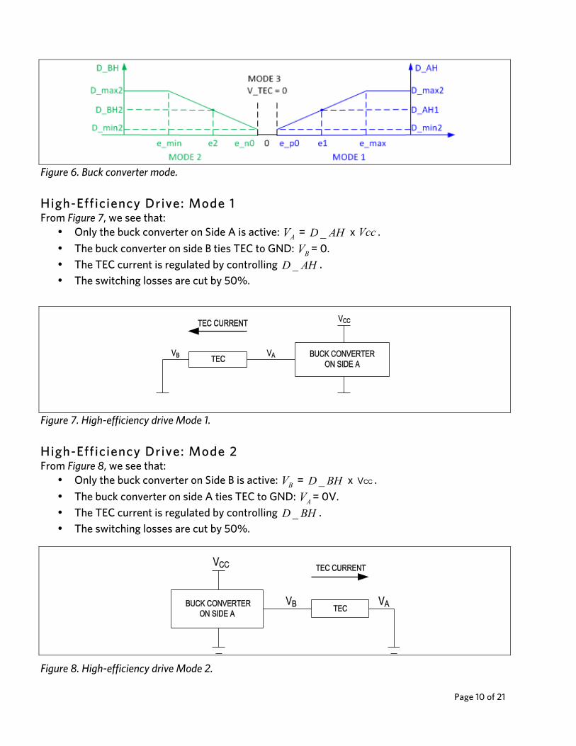
Once we obtain ][_ nPIe , we can determine the PWM duty cycles. The following section explains the procedure. Intell igent Drive, One Buck Converter The DS4830A selects the drive mode shown in Figure 6 based on the current-loop output. Below are a few notes:
1) Only one buck converter is active in mode 1 and 2. 2) Neither buck converter is active in mode 3. 3) Switching losses are cut by 50%.
i_set[n]
+
i_TEC[n]
i_err[n] PIFILTER
PWMGENERATOR
BUCKREGULATORS
e_PI[n]
Page 10 of 21
Figure 6. Buck converter mode. High-Efficiency Drive: Mode 1 From Figure 7, we see that:
• Only the buck converter on Side A is active: AV = AHD _ x Vcc . • The buck converter on side B ties TEC to GND: BV = 0. • The TEC current is regulated by controlling AHD _ . • The switching losses are cut by 50%.
Figure 7. High-efficiency drive Mode 1. High-Efficiency Drive: Mode 2 From Figure 8, we see that:
• Only the buck converter on Side B is active: BV = BHD _ x CCV . • The buck converter on side A ties TEC to GND: AV = 0V. • The TEC current is regulated by controlling BHD _ . • The switching losses are cut by 50%.
Figure 8. High-efficiency drive Mode 2.
Page 11 of 21
Determine PWM Duty Cycles In Mode 1 We take a closer look at the H-bridge shown in Figure 4. The output voltage of the buck converter on Side A, AV , can be approximately expressed as:
CCSW
ONQAHA V
TT
V _= (Eq. 16)
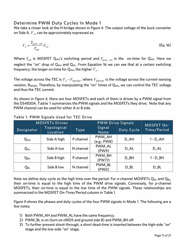
Where SWT is MOSFET QAH’s switching period and ONQAHT _ is the on-time for QAH. Here we neglect the “on” drop of QAH and QAL. From Equation 16 we can see that at a certain switching frequency, the longer on-time for QAH, the higher AV . The voltage across the TEC is RSENSEA VV − , where RSENSEV is the voltage across the current-sensing resistor, RSENSE. Therefore, by manipulating the “on” times of QAH, we can control the TEC voltage and thus the TEC current. As shown in Figure 4, there are four MOSFETs and each of them is driven by a PWM signal from the DS4830A. Table 1 summarizes the PWM signals and the MOSFETs they drive. Note that any PWM channel can be used for either A or B side. Table 1. PWM Signals Used for TEC Drive
MOSFETs Driven PWM Drive Signals MOSFET On-Time/Period Designator Topological
Location Type Signal Name Duty Cycle
QAH Side A high P channel PWM_AH (e.g.: PW8) D_AH 1 - D_AH
QAL Side A low N channel PWM_AL (PW9) D_AL D_AL
QBH Side B high P channel PWM_BH (PW7)1 D_BH 1 - D_BH
QBL Side B low N channel PWM_BL (PW0) D_BL D_BL
Note we define duty cycle as the high time over the period. For n-channel MOSFETs QAL and QBL, their on-time is equal to the high time of the PWM drive signals. Conversely, for p-channel MOSFETs, their on-time is equal to the low time of the PWM signals. These relationships are summarized in the MOSFET On-Time/Period column in Table 1. Figure 9 shows the phases and duty cycles of the four PWM signals in Mode 1. The following are a few notes:
1) Both PWM_AH and PWM_AL have the same frequency. 2) PWM_BL is on (turn on nMOS and ground side B) and PWM_BH off. 3) To further prevent shoot-through, a short dead-time is inserted between the high-side “on”
stage and the low-side “on” stage.

Page 12 of 21
4) According to Figure 9, ALD _ can be expressed in terms of AHD _ . If we let DT denote the ratio between the dead-time and the PWM period, we have:
DTAHDALD ×−= 2__ (Eq. 17)
Figure 9. PWM phases and duty cycles in Mode 1. Before we explain how to determine D_AH, we define the TEC current flowing from Side A to Side B as positive. Similarly, we define the TEC voltage as positive in Mode 1. Assume for a moment that the TEC current ][_ nTECi is less than the target TEC current
][_ nseti . Then the current error ][_][_][_ nTECinsetinerri −= is greater than zero. Subject to the proportional and integral gains, this positive ][_ nerri will gradually drive the output of the PI controller ][_ nPIe up. Consequently, as shown in Figure 4, AV needs to increase and BV needs to be grounded in order for ][_ nTECi to catch up with ][_ nseti . Reviewing Equation 16, the on-time of QAH needs to increase so AV can go up. To summarize the analysis above, a less than target TEC current results in a positive ][_ nerri , which drives ][_ nPIe up, and a longer ONQAHT _ is needed to boost the TEC current. Figure 10 illustrates the intuitive relationship between ][_ nPIe and ONQAHT _ for a closed-loop TEC current control.
D_AH (PWM_AH)
D_AL (PWM_AL)
D_BH (PWM_BH)
D_BL (PWM_BL)
PMOS
PMOS
NMOS
NMOS
ON OFF ON OFF
OFF
ON
ONOFF ON OFF
DEAD-‐TIME
COMPLEMENTARY

Page 13 of 21
Figure 10. TQAH_ON vs. e_PI[n]. The fundamental relationship is: the larger e_PI[n], the longer TQAH_ON. Note that we have introduced limits (e_max and e_min) for e_PI[n] and TQAH_ON to avoid integral windup and reduce overshooting. Thus, e_PI[n] will be clamped to e_max if it becomes greater than e_max. Similarly, if e_PI[n] goes below e_min, it will be clamped to e_min. Although the duty cycle of the buck converter can run from 0 to 100%, it is good practice to keep the PWM duty cycles within a certain range. As shown in Figure 10, T_min denotes the minimum available on-time for QAH and it corresponds to e_min. At the other end, T_max denotes the maximum available on-time for QAH and it corresponds to e_max. We assume TQAH_ON increases linearly as e_PI[n] increases. Then it is simple math to calculate TQAH_ON according to Figure 10.
min_min)_max_(min_max_min_][_
_ TTTeeenPIeT ONQAH +−
−
−= (Eq. 18)
Once TQAH_ON is determined using Equation 18, D_AH can be calculated using the relationship shown in Table 1 and D_AL can be obtained using Equation 17. Then one can set up the PWM channels and drive the TEC accordingly. Note: In Mode 2, D_BH and D_BL can be calculated in a similar way.

Page 14 of 21
Summary This application note detailed how to control a TEC using the DS4830A optical microcontroller. We first converted a prototype analog controller’s transfer function to the discrete domain using bilinear transformation. Then a PI controller was presented for the current loop. All procedures and their implementation using the DS4830A were systematically explained. For further information, lab results and an example code are provided in Appendix C and Appendix D, respectively.

Page 15 of 21
Appendix A: Expressions for Gc(z) and GF(z) In Part II, we omitted the analytical expressions for GC(z) and GF(z) for the sake of succinctness. The expressions are laid out here. Plugging Equation 8 into Equation 3, we have:
1])
11(4)(
1121[
112)(
)()11(4)(
1121
)()()(
182
21817
18162
218161 −
+−
+++−
++−
+
++−
++++−
+−==
ττττττ
ττττττ
aac
bb
errC
zz
Tzz
Tzz
T
zz
Tzz
TzvzvzG (Eq. 19)
Where:
2316 CR=τ , 3217 CR=τ , 1118 CR=τ , 33CRa =τ , 12CRb =τ , and 22CRc =τ .
Define the following intermediate variables:
)(4)(21 1816218163 bb TTa ττττττ +++++= ,
)(4)(23 1816218162 bb TTa ττττττ +−+++= ,
)(4)(23 1816218161 bb TTa ττττττ +−++−= ,
)(4)(21 1816218160 bb TTa ττττττ ++++−= ,
1817318172173 )(8))((4)(2 ττττττττττ acacc TTTb ++++++= ,
1817318172172 )(24))((4)(2 ττττττττττ acacc TTTb +−++−+= ,
1817318172171 )(24))((4)(2 ττττττττττ acacc TTTb ++++−+−= , and
1817318172170 )(8))((4)(2 ττττττττττ acacc TTTb +−++++−= ,
Now we can simplify Equation 20 to:
012
23
3
00112
223
331 )()()()()()()(
bzbzbzbbazbazbazba
zvzvzG
errC +++
+++++++−== (Eq. 20)
Page 16 of 21
After taking the inverse z-transform of Equation 21, we have Equation 9. The associated digital filter coefficients can be determined using the Excel calculator presented in Appendix B. Similar to the process above, we can obtain the expression for GF(z). Plugging Equation 8 into Equation 4, we have:
)1121)(
1121(
1121
1)()()(
18
16
32
12
+−
++−
+
+−
+
++==
zz
Tzz
T
zz
TCC
CzvzvzG
aset
F
ττ
τ (Eq. 21)
Define the following intermediate variables:
)21( 1632
12 τ
TCCCc ++
= ,
32
11
2CCCc+
= ,
)21( 1632
10 τ
TCCCc −+
= ,
1821824)(21 ττττ aa TT
d +++= ,
182182 ττ aT
d −= , and
1821804)(21 ττττ aa TT
d ++−= ,
Now we can simplify Equation 22 to:
012
2
00112
222 )()()()()()(
dzdzddczdczdc
zvzvzG
setF ++
+++++== (Eq. 22)
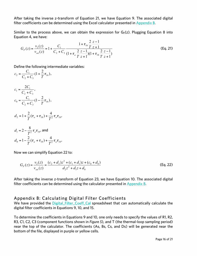
After taking the inverse z-transform of Equation 23, we have Equation 10. The associated digital filter coefficients can be determined using the calculator presented in Appendix B. Appendix B: Calculating Digital Fi lter Coefficients We have provided the Digital_Filter_Coeff_Cal spreadsheet that can automatically calculate the digital filter coefficients in Equations 9, 10, and 15. To determine the coefficients in Equations 9 and 10, one only needs to specify the values of R1, R2, R3, C1, C2, C3 (component functions shown in Figure 5), and T (the thermal-loop sampling period) near the top of the calculator. The coefficients (As, Bs, Cs, and Ds) will be generated near the bottom of the file, displayed in purple or yellow cells.
Page 17 of 21
Similarly, one only needs to specify Kp, KI, and Tc in cells D88 to D90 to calculate the coefficients in Equation 15. This information will be provided in cells D92 to D94. Appendix C: Lab Results We ran the example code on a DS4830A Evaluation Kit board to get transient responses and H-bridge efficiency.
A. Transient Responses Figure 11 shows the transient responses. The yellow curve is the set-point voltage and the red curve is the thermistor voltage.
The experiment setup and procedures follow:
1) A transmitter optical subassembly (TOSA) mounted on a heatsink. The TOSA has a
built-in TEC and thermistor. 2) DC power supplies:
a. 3.3V for the EV board b. Variable DC supply for the set-point voltage
3) Connections: a. Connect TEC (+) of the TOSA to the R_TECC pad next to jumper LOADA on the
EV kit board. b. Connect TEC (-) of the TOSA to the R_TECC pad next to jumper LOADB on the
EV kit board. c. Connect the thermistor signal of the TOSA to test point TECC_TEMP on the EV
kit board. d. Connect TOSA ground to EV kit board ground. e. Connect the set-point voltage to ADC_D7P and ground to ADC_D7N on the EV
kit board. 4) Power-on sequence:
a. Power on the DS4830A EV kit. b. Turn on the set-point voltage with an initial value of 0.75V.
5) Testing the TEC control functionality: a. Decrease the set-point voltage to 0.40V and wait for the thermistor voltage to
settle. b. Increase the set-point voltage back to 0.75V and wait for the thermistor voltage
to settle.
Page 18 of 21
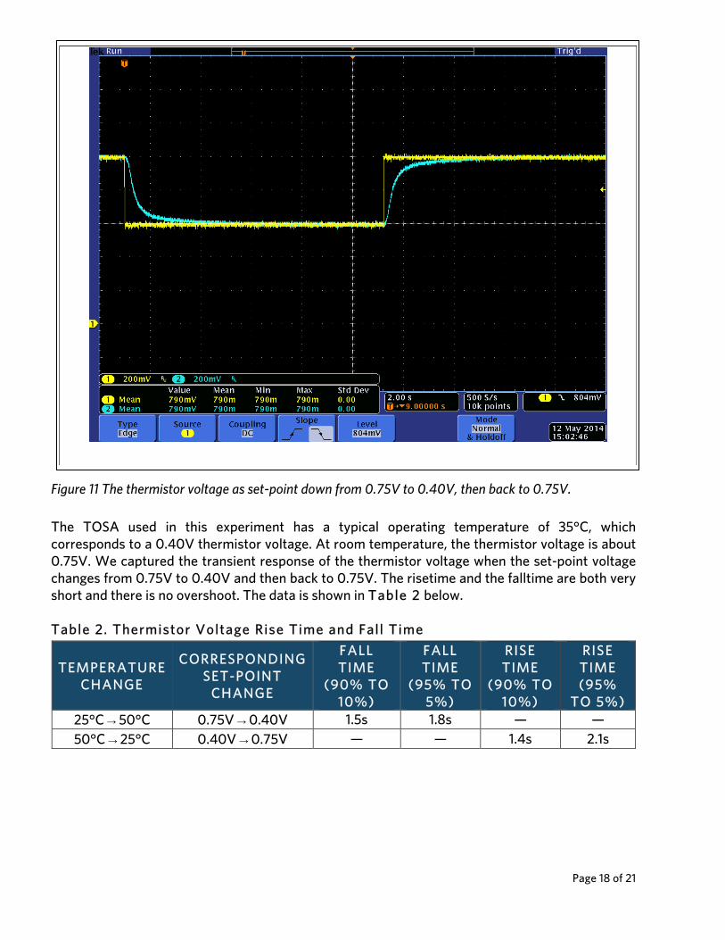
Figure 11 The thermistor voltage as set-point down from 0.75V to 0.40V, then back to 0.75V. The TOSA used in this experiment has a typical operating temperature of 35°C, which corresponds to a 0.40V thermistor voltage. At room temperature, the thermistor voltage is about 0.75V. We captured the transient response of the thermistor voltage when the set-point voltage changes from 0.75V to 0.40V and then back to 0.75V. The risetime and the falltime are both very short and there is no overshoot. The data is shown in Table 2 below. Table 2. Thermistor Voltage Rise Time and Fall Time
TEMPERATURE CHANGE
CORRESPONDING SET-POINT
CHANGE
FALL TIME
(90% TO 10%)
FALL TIME
(95% TO 5%)
RISE TIME
(90% TO 10%)
RISE TIME (95%
TO 5%) 25°C → 50°C 0.75V → 0.40V 1.5s 1.8s — — 50°C → 25°C 0.40V → 0.75V — — 1.4s 2.1s

Page 19 of 21
B. Efficiency Figure 12 shows the H-bridge efficiency.
Figure 12. DS4830A TEC EV kit H-bridge efficiency.
The experiment setup and procedures follow:
1) One 3.3 or 3.6V power supply (VCC) for the EV kit board.
2) Disable H-bridge (Remove J8, J9, and J10 jumpers) and measure power-supply output current, ICQ
3) Connect a 1.3Ω or 2.2Ω resistor, RLOAD, as a dummy load on J10 jumper.
4) Set ‘gucIsetDebugEnable’ to 1 and set ‘gfIsetDebug’ in firmware to different values (0.1A to 0.8A) and run the code on the EV kit board. Record the power-supply ouput current, IS.
5) H-bridge input current is: IIN = IS - ICQ
6) Efficiency = (gfIsetDebug x gfIsetDebug x RLOAD)/(IIN × VCC)
0%
10%
20%
30%
40%
50%
60%
70%
80%
0.1 0.2 0.4 0.6 0.8 0.9
H-BR
IDGE
EFF
ICIE
NCY
TEC CURRENT (A)
DS4830A TECC EV KIT H-BRIDGE EFFICIENCY
1.3Ω LOAD
2.2Ω LOAD
1.3Ω, 3.6V
LEADING ANALOG TEC CONTROLLER, 1.3Ω LOAD

Page 20 of 21
C. Long Term Wavelength and Power Drift
We ran long hours (about 64 hours) wavelength drift and power test. Agilent 86120C Multi-Wavelength Meter was used to measure the result. The wavelength reference is 1535.3 nm and the power one 0.73 db. The total wavelength drift is 12 pm from the reference and the laser power 0.11 db since the drift measurement was started. Values represent the minimum wavelength drift and power drift values subtracted from the maximum drift values. They are excellent results. Table 3. Long Term Test Results
Test Running Hours
Reference Wavelength
Reference Laser Power
Max. Wavelength Drift
Max Laser Power Drift
64 1535.3 nm 0.73 db 12 pm 0.11 db The experiment setup and procedures follow: 1) A transmitter optical subassembly (TOSA) mounted on a heatsink. The TOSA has a
built-in TEC and thermistor.
2) DC power supplies: a. 3.3V for the EV board b. A second current source (about 30 mA) for the TOSA Ibias
3) Remove the J6 Jumper. Connect the 2nd current source (+) to the pin closer to the
DS4830A socket and (-) to the ground of the PCB.
4) Connect a single mode (yellow) optical fiber cable from TOSA to the Optical Input of the Wavelength Meter.
5) Turn on both powers and wait a few minutes for the laser to stabilize. Start the test.
D. Wavelength and Power Drift Under Extreme Temperature The following table shows the extreme temperature (-40 -> +85°) wavelength drift and power test result. We used Agilent 86120C Multi-Wavelength Meter to measure the result and an oven to change the temperature. The wavelength reference is 1535.385 nm and the power one -0.1 db at 25°. During tests, we kept the oven temperature for at least 30 minutes at -40° and 85°. The total wavelength drift is 24 pm from the reference and the laser power 0.27 db since the drift measurement was started. Values represent the minimum wavelength drift and power drift values subtracted from the maximum drift values. They are excellent results.

Page 21 of 21
Table 4. Extreme Temperature Test Results Temperature Range
Reference Wavelength at 25°
Reference Laser Power at 25°
Max. Wavelength Drift
Max Laser Power Drift
-40° -> +85° 1535.385 nm -0.1db 24 pm 0.27
The experiment setup and procedures are as the same as the test for Long Term Wavelength and Power Drift except that the PCB and TOSA has to be put inside the Oven and the test also doesn’t need to run long hours.
Appendix D: Example Code For the source code (in C) of our DS4830A TEC driver, please contact Maxim support. It should be noted that our code was customized for the lab setup described in Appendix C, which means that all the parameters, coefficients, and configurations are based on that particular setup. Users should NOT try running the code directly on their own TEC control board. Excel is a registered trademark of Microsoft Corporation.