Embed Size (px)
Citation preview
2678 IEEE TRANSACTIONS ON VERY LARGE SCALE INTEGRATION (VLSI) SYSTEMS, VOL. 25, NO. 9, SEPTEMBER 2017
Thermomechanical Stress-Aware Management for 3-D IC DesignsQiaosha Zou, Member, IEEE, Eren Kursun, Senior Member, IEEE, and Yuan Xie, Fellow, IEEE
Abstract— Thermal characteristics have been considered as one of themost challenging problems in 3-D integrated circuits (3-D ICs). Dueto the thermal expansion coefficient mismatch between through-siliconvias (TSVs) and the silicon substrate, and the presence of elevated thermalgradients, thermomechanical stress issues are exacerbated in 3-D ICs.In this brief, we propose a solution that combines design-time and run-time techniques to reduce thermomechanical stress and the associatedreliability issues. A TSV stress-aware floorplan policy is proposed tominimize the possibility of wafer cracking and interfacial delamination.In addition, a run-time thermal management scheme effectively elimi-nates large thermal gradients between layers. Experimental results showthat the reliability of 3-D design can be significantly improved due to thereduced TSV thermal load and the elimination of mechanical damagingthermal cycling pattern. Moreover, impacts of thermal characteristics inTSVs and thermal vias insertion are explored.
Index Terms— 3-D integrated circuits (3-D ICs), mechanicalreliability, thermal cycling, thermal management, thermome-chanical stress.
I. INTRODUCTION
The 3-D integrated circuits (3-D ICs) have been shown to providenumerous advantages in achieving better performance for futurecomputing sytsems [1], [2]. However, the increased power densityand decreased chip footprint induce thermal issue, which is widelyconsidered as one of the biggest challenges in 3-D designs [3], [4].
In addition to temperature increases, the coefficient of ther-mal expansion (CTE) mismatch exacerbates thermal stresses in3-D circuits. Merely using design-time solution is insufficient towardthermal stress problem, because the dynamic thermal gradient cannotbe captured. To this end, 3-D IC designs should carefully take intoaccount the aforementioned thermal challenges in both design-timeand run-time. Unfortunately, little work has been done to alleviatethe challenge through these two stages. In this brief, we proposea two-stage, design-time and run-time solution to this problem.The proposed two-stage thermal management methodology can besummarized as follows.
1) Design-time thermal stress-aware floorplan to reduce thethrough-silicon via (TSV) thermal load in addition to the wholechip temperature and minimize thermomechanical stresses.
2) Run-time thermal management scheme to analyze thermalcycling patterns and control thermal gradients, thus to lowermechanical stresses on chip and eventually achieve mechanicalequilibrium among layers.
II. BACKGROUND AND RELATED WORK
Stacked chips on 3-D architecture increase the packaging den-sity and thermal resistances, which results in higher on-chip
Manuscript received October 8, 2016; revised March 7, 2017; acceptedApril 28, 2017. Date of publication June 22, 2017; date of current versionAugust 23, 2017. (Corresponding author: Qiaosha Zou.)
Q. Zou is with the Department of Computer Science, Zhejiang Uni-versity of Science and Technology, Hangzhou 310000, China (e-mail:[email protected]).
E. Kursun is with Columbia University, New York, NY 10027 USA (e-mail:[email protected]).
Y. Xie is with the Department of Electrical and Computer Engineering,University of California at Santa Barbara, Santa Barbara, CA 93106 USA(e-mail: [email protected]).
Color versions of one or more of the figures in this paper are availableonline at http://ieeexplore.ieee.org.
Digital Object Identifier 10.1109/TVLSI.2017.2707119
temperatures. Extensive studies have been done by focusing on the3-D thermal modeling, analysis [5], [6], and thermal-aware designmethodology [7], [8] to manage the on-chip thermal issues of3-D ICs. However, the TSV lateral thermal blockage effect and thesilicon fatigue due to thermomechanical stresses were not consideredin previous work. On the other hand, prior work on analyzing themechanical stresses in 3-D ICs [9], [10] only consider the staticstress management by adjusting TSV keep-out zone size, TSV place-ment, or TSV structure. Distinguished from previous work, this briefnot only accounts for the static (design-time) management of thermalstress and thermal load but also takes into account the run-time stressanalysis and management.
A. Analysis of TSV Thermal Effects
To minimize the chip temperature and thermomechanical stresses-induced fatigue, the placement of TSV farms can be optimized duringdesign time. Two of the TSV thermal effects should be considered:TSV thermomechanical stresses and lateral thermal blockage effect.
1) TSV Thermomechanical Stresses: In 3-D IC fabrication,copper (Cu) is usually used as TSV filling material that has morethan five times larger CTE than silicon. The CTE mismatch betweenTSV and silicon substrate in turn introduces mechanical stressesthat can lead to high probability of die cracking and interfacialdelamination [11], [12]. Their study suggested that the stresses inTSVs are proportional to the thermal load and CTE mismatch. Andthe stresses can be represented by radial σr , circumferential σθ , andaxial stresses σz , which has the following expression:
σr = σθ = −E(αtsv − αsi)Ttsv
2 − 2υ, σz = 2σθ (1)
where αtsv is the CTE of TSVs and αsi denotes the CTE of silicon.Ttsv is the thermal load on TSVs, which can be calculated as thedifference between TSV temperature and room temperature. E isYoung’s modulus and υ is Poisson’s ratio.
When the material and diameter of TSVs are determined, andthe other parameters are constant, and therefore, the only variableis TSVs’ thermal load. Therefore, the proposed design-time thermalmanagement scheme alleviates thermomechanical stresses by reduc-ing the thermal load on TSVs.
2) TSV Lateral Thermal Blockage Effect: TSV lateral thermalblockage effect is found due to the unequal thermal conductivitiesin vertical and horizontal directions [6]. Specifically, the liner layerbetween TSV filling material and silicon substrate has higher thermalresistance. Therefore, the lateral thermal dissipation path is blockedby liner layers. The thermal dissipation capability of TSV can bemodeled with three factors: thickness of the material, thermal con-ductivity of the corresponding material per unit volume, and the areaof the corresponding material. Then, the lateral thermal resistancecan be calculated from the thermal resistance of TSV filling, linermaterials, and silicon substrate [13].
B. 3-D Thermal Cycling Effect
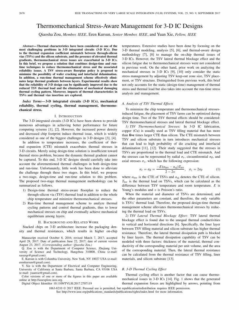
Thermal cycling effect is another factor that can cause thermo-mechanical issues in 3-D ICs [14]. Fig. 1 shows that the generatedthermal expansion forces are highlighted by arrows, pointing from
1063-8210 © 2017 IEEE. Personal use is permitted, but republication/redistribution requires IEEE permission.See http://www.ieee.org/publications_standards/publications/rights/index.html for more information.
IEEE TRANSACTIONS ON VERY LARGE SCALE INTEGRATION (VLSI) SYSTEMS, VOL. 25, NO. 9, SEPTEMBER 2017 2679
Fig. 1. Stack level thermal cycling effect in 3-D structure. Thermal stressesare pointing from hot blocks (dark color) to cool blocks (light color).Alternating direction of stresses (the arrows) easily cause fatigue or evencracking on thinned substrate.
the hotter blocks to the cooler blocks. As shown, the temperaturein blocks 2, 4, and 6 is higher than that of blocks 1, 3, and 5. Thecorresponding forces labeled 1 and 3 are in the opposite directionwith force 2. Forces in opposite directions cause fatigue in the stackedchips and make the thinned silicon substrate more vulnerable to becracked. A run-time thermal cycling management scheme is proposedto eliminate the damaging thermal cycling pattern by using dynamicpower scaling.
III. THERMOMECHANICAL STRESS-AWARE 3-DDESIGN METHODOLOGY
A. Themomechanical Stress Aware Design Time Algorithm
The purpose of the design-time thermal stress-aware TSV man-agement aims at reducing the CTE-induced thermomechanical stress,which can be translated into the minimization of the TSVs thermalload and chip temperature.
Intuitively, placing TSVs away from hot regions can reduce theirthermal load. However, in most scenarios, hotspots are functionalunits that are frequently activated and highly utilized, indicating highrequirements for connectivity. Timing/performance and other designgoals prevent moving TSV farms away from those hotspots. As aresult, the thermal stress-aware floorplan is obligatory to sustain thehigh circuit performance without causing severe thermal reliabilityproblems.
In addition to the traditional floorplan solutions that make greatefforts on balancing the area and performance tradeoff, the proposedfloorplan flow also strives to minimize the thermal-induced stresses.Circuit description and average power consumption of each block aregiven as inputs. The circuit description consists of block descriptionsand the connectivity information. The average power consumptionof each block is then estimated from the power density on the chip.TSV farms are treated as soft blocks in the floorplan with giventhermal characteristics described in Section II.
A simulated annealing-based floorplanner is employed in the flowalong with an analytical initial floorplan to speed up the conver-gence. The circuit is partitioned into required tiers by balancing theTSV number and chip area. Then, the initial floorplan is performedanalytically by placing the modules that have low power densityaround TSV farm. The TSV and tier temperature are generatedcorrespondingly. After the initial floorplan, modules are randomlyselected, permuted, and adjusted aspect ratio to obtain a better thermaldistribution across the whole chip. Changing the aspect ratio ofTSV farm means adjusting the arrangement of TSVs, resulting inbetter lateral thermal path for better heat dissipation.
A cost function is associated considering the chip area, averagetemperature, TSV farms’ temperature, and wire length. After eachiteration, the cost is calculated based on the floorplan thermal profileto guide the floorplan. The iteration process terminates once theSA convergence condition is satisfied or maximum iteration step isreached.
B. Thermal Cycling-Aware Run-Time Management
Run-time thermal cycling management scheme is devised asthe second stage to achieve 3-D architecture mechanical equilibriumby eliminating mechanical damaging cycling patterns as illustratedin Section II.
The run-time management is performed in a bottom-up, layer-by-layer fashion. Each tier is partitioned in fine-granularity, and thetemperature of each grid is monitored by thermal sensors in runtime.If sensors are not applicable, the thermal profile can be obtained withthe power trace derived from the supply voltage and activity factorof each block.
The first step controls the temperature gradients of each gridto eliminate large temperature gradients between adjacent grids.1
Correspondingly, mechanical force vectors are generated based onthese adjacent temperature gradients. On the other hand, predefinedthresholds are determined based on the TSV size, material, andsubstrate thickness. The force vectors is then compared with thepredefined thresholds; if force vectors are larger than thresholds,dynamic power scaling techniques, such as DVFS, will be deployedto control the thermal dissipation of hot grids.
In addition to temperature gradients, the thermal cycling patternis another dynamic parameter that should be handled carefully. Thecycling pattern is taken into account by comparing force vectorsof neighboring grids in two adjacent layers. If the thermal cyclingpattern is in an alternating way as described in Fig. 1, powermanagement is applied to the higher temperature regions to lowerthe resulting thermal mechanical stresses and achieve mechanicalequilibrium. The power scaling results in a new thermal cyclingpattern in the stack, which may require further adjustment in thenext sampling interval until the whole stack reaches the mechanicalequilibrium state.
IV. EXPERIMENTAL RESULTS AND ANALYSIS
To evaluate the proposed thermal management mechanism, a typ-ical 3-D floorplanner (3DFP) [15] that aims at reducing the averageon-chip temperature is employed as our baseline. We successfullyimplemented the thermal stress-aware floorplan mechanism in 3DFP.We also extended Hotspot [16] to estimate 3-D on-chip temperaturewith detailed modeling on TSV lateral and vertical thermal con-ductivities. MCNC benchmarks and one 3-D stacking system withfour cores and shared L2 cache are leveraged in the block-level andsystem-level evaluations. We differentiated the block-level simulationand the system-level simulation, since they have distinct thermalcharacteristics. The temperature gradients at block level are largerand more unpredictable due to various features of the underlyingcircuits, while the temperature distribution at system level is usuallyuniform and predictable because of the relatively regular placementof functional modules.
The thermal parameters used in the experiment are listed in Table I.The default TSV diameter is 10 μm. Since the TSV farm size andarrangement are different in each circuit for block-level evaluation,we calculated the corresponding vertical and lateral thermal resis-tivities with the model proposed in [13] and used them as inputparameters for the floorplan. In addition to the mechanism evaluation,we varied the TSV lateral thermal conductivity and TSV diameterfor the sensitivity study. For simplicity, the elastic mismatch betweensilicon and copper is neglected.
A. Block-Level Thermomechanical Stress-Aware Floorplan
To quantify the TSV thermal load reduction from the stress-aware floorplan, we conducted experiments on five MCNC floorplan
1In this brief, the temperature differences between grids are used to representtemperature gradients for simplicity.
2680 IEEE TRANSACTIONS ON VERY LARGE SCALE INTEGRATION (VLSI) SYSTEMS, VOL. 25, NO. 9, SEPTEMBER 2017
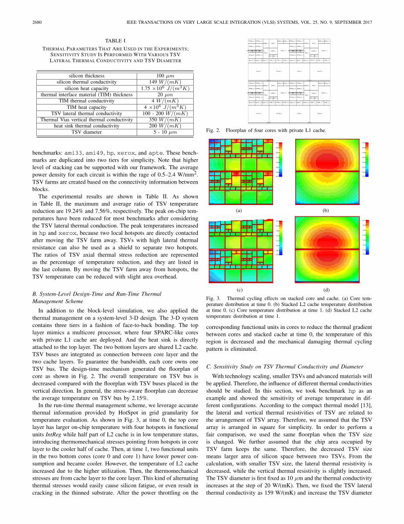
TABLE I
THERMAL PARAMETERS THAT ARE USED IN THE EXPERIMENTS;SENSITIVITY STUDY IS PERFORMED WITH VARIOUS TSVLATERAL THERMAL CONDUCTIVITY AND TSV DIAMETER
benchmarks: ami33, ami49, hp, xerox, and apte. These bench-marks are duplicated into two tiers for simplicity. Note that higherlevel of stacking can be supported with our framework. The averagepower density for each circuit is within the rage of 0.5–2.4 W/mm2.TSV farms are created based on the connectivity information betweenblocks.
The experimental results are shown in Table II. As shownin Table II, the maximum and average ratio of TSV temperaturereduction are 19.24% and 7.56%, respectively. The peak on-chip tem-peratures have been reduced for most benchmarks after consideringthe TSV lateral thermal conduction. The peak temperatures increasedin hp and xerox, because two local hotspots are directly contactedafter moving the TSV farm away. TSVs with high lateral thermalresistance can also be used as a shield to separate two hotspots.The ratios of TSV axial thermal stress reduction are representedas the percentage of temperature reduction, and they are listed inthe last column. By moving the TSV farm away from hotspots, theTSV temperature can be reduced with slight area overhead.
B. System-Level Design-Time and Run-Time ThermalManagement Scheme
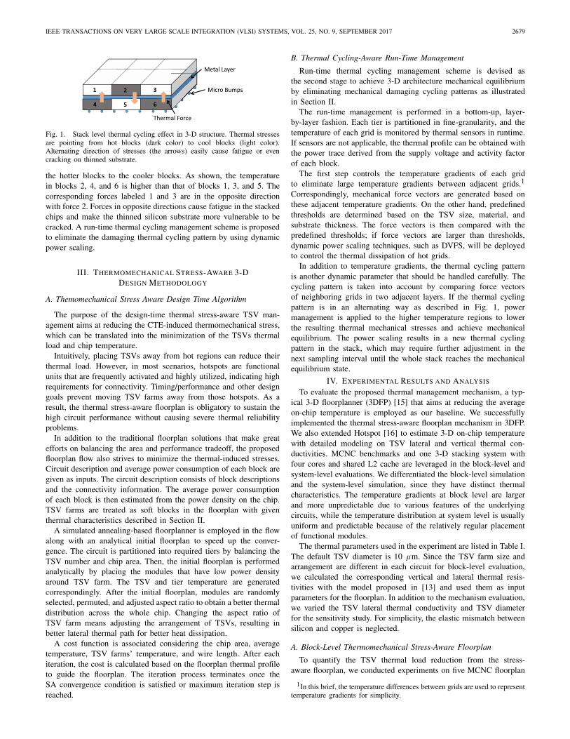
In addition to the block-level simulation, we also applied thethermal management on a system-level 3-D design. The 3-D systemcontains three tiers in a fashion of face-to-back bonding. The toplayer mimics a multicore processor, where four SPARC-like coreswith private L1 cache are deployed. And the heat sink is directlyattached to the top layer. The two bottom layers are shared L2 cache.TSV buses are integrated as connection between core layer and thetwo cache layers. To guarantee the bandwidth, each core owns oneTSV bus. The design-time mechanism generated the floorplan ofcore as shown in Fig. 2. The overall temperature on TSV bus isdecreased compared with the floorplan with TSV buses placed in thevertical direction. In general, the stress-aware floorplan can decreasethe average temperature on TSV bus by 2.15%.
In the run-time thermal management scheme, we leverage accuratethermal information provided by HotSpot in grid granularity fortemperature evaluation. As shown in Fig. 3, at time 0, the top corelayer has larger on-chip temperature with four hotspots in functionalunits IntReg while half part of L2 cache is in low temperature status,introducing thermomechanical stresses pointing from hotspots in corelayer to the cooler half of cache. Then, at time 1, two functional unitsin the two bottom cores (core 0 and core 1) have lower power con-sumption and became cooler. However, the temperature of L2 cacheincreased due to the higher utilization. Then, the thermomechanicalstresses are from cache layer to the core layer. This kind of alternatingthermal stresses would easily cause silicon fatigue, or even result incracking in the thinned substrate. After the power throttling on the
Fig. 2. Floorplan of four cores with private L1 cache.
Fig. 3. Thermal cycling effects on stacked core and cache. (a) Core tem-perature distribution at time 0. (b) Stacked L2 cache temperature distributionat time 0. (c) Core temperature distribution at time 1. (d) Stacked L2 cachetemperature distribution at time 1.
corresponding functional units in cores to reduce the thermal gradientbetween cores and stacked cache at time 0, the temperature of thisregion is decreased and the mechanical damaging thermal cyclingpattern is eliminated.
C. Sensitivity Study on TSV Thermal Conductivity and Diameter
With technology scaling, smaller TSVs and advanced materials willbe applied. Therefore, the influence of different thermal conductivitiesshould be studied. In this section, we took benchmark hp as anexample and showed the sensitivity of average temperature in dif-ferent configurations. According to the compact thermal model [13],the lateral and vertical thermal resistivities of TSV are related tothe arrangement of TSV array. Therefore, we assumed that the TSVarray is arranged in square for simplicity. In order to perform afair comparison, we used the same floorplan when the TSV sizeis changed. We further assumed that the chip area occupied byTSV farm keeps the same. Therefore, the decreased TSV sizemeans larger area of silicon space between two TSVs. From thecalculation, with smaller TSV size, the lateral thermal resistivity isdecreased, while the vertical thermal resistivity is slightly increased.The TSV diameter is first fixed as 10 μm and the thermal conductivityincreases at the step of 20 W/(mK). Then, we fixed the TSV lateralthermal conductivity as 159 W/(mK) and increase the TSV diameter
IEEE TRANSACTIONS ON VERY LARGE SCALE INTEGRATION (VLSI) SYSTEMS, VOL. 25, NO. 9, SEPTEMBER 2017 2681
TABLE II
DESIGN TIME THERMOMECHANICAL STRESS-AWARE FLOORPLAN EXPERIMENTAL RESULTS
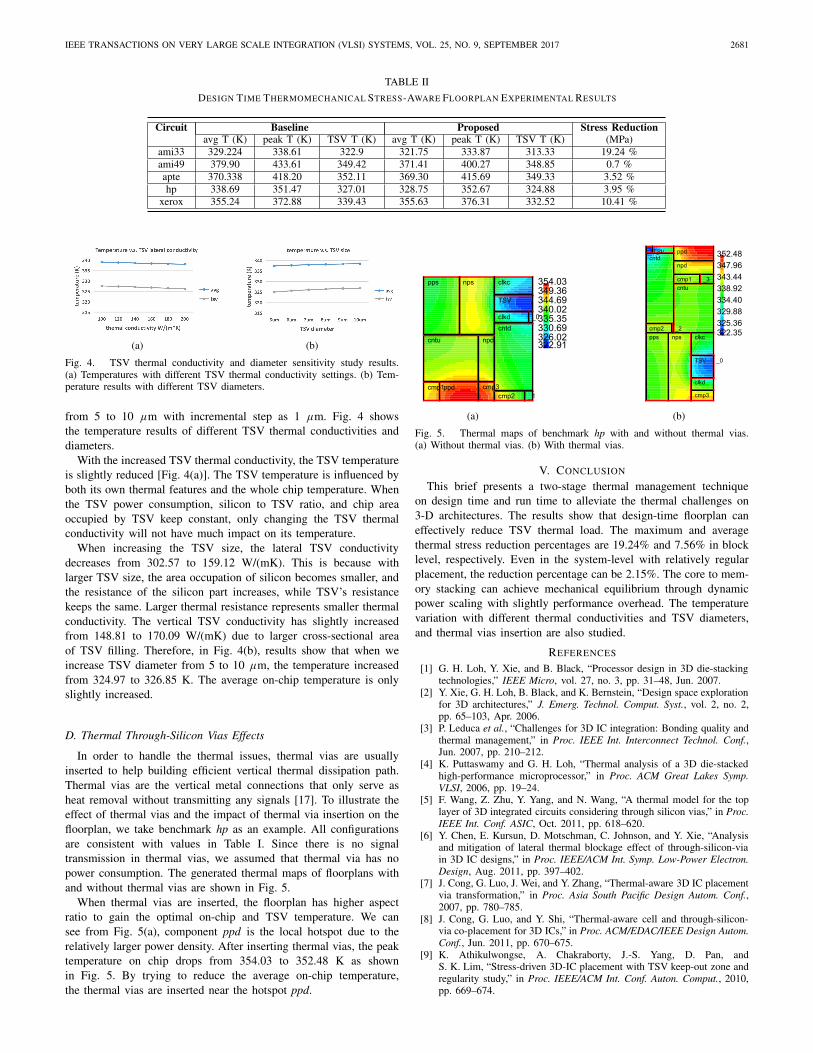
Fig. 4. TSV thermal conductivity and diameter sensitivity study results.(a) Temperatures with different TSV thermal conductivity settings. (b) Tem-perature results with different TSV diameters.
from 5 to 10 μm with incremental step as 1 μm. Fig. 4 showsthe temperature results of different TSV thermal conductivities anddiameters.
With the increased TSV thermal conductivity, the TSV temperatureis slightly reduced [Fig. 4(a)]. The TSV temperature is influenced byboth its own thermal features and the whole chip temperature. Whenthe TSV power consumption, silicon to TSV ratio, and chip areaoccupied by TSV keep constant, only changing the TSV thermalconductivity will not have much impact on its temperature.
When increasing the TSV size, the lateral TSV conductivitydecreases from 302.57 to 159.12 W/(mK). This is because withlarger TSV size, the area occupation of silicon becomes smaller, andthe resistance of the silicon part increases, while TSV’s resistancekeeps the same. Larger thermal resistance represents smaller thermalconductivity. The vertical TSV conductivity has slightly increasedfrom 148.81 to 170.09 W/(mK) due to larger cross-sectional areaof TSV filling. Therefore, in Fig. 4(b), results show that when weincrease TSV diameter from 5 to 10 μm, the temperature increasedfrom 324.97 to 326.85 K. The average on-chip temperature is onlyslightly increased.
D. Thermal Through-Silicon Vias Effects
In order to handle the thermal issues, thermal vias are usuallyinserted to help building efficient vertical thermal dissipation path.Thermal vias are the vertical metal connections that only serve asheat removal without transmitting any signals [17]. To illustrate theeffect of thermal vias and the impact of thermal via insertion on thefloorplan, we take benchmark hp as an example. All configurationsare consistent with values in Table I. Since there is no signaltransmission in thermal vias, we assumed that thermal via has nopower consumption. The generated thermal maps of floorplans withand without thermal vias are shown in Fig. 5.
When thermal vias are inserted, the floorplan has higher aspectratio to gain the optimal on-chip and TSV temperature. We cansee from Fig. 5(a), component ppd is the local hotspot due to therelatively larger power density. After inserting thermal vias, the peaktemperature on chip drops from 354.03 to 352.48 K as shownin Fig. 5. By trying to reduce the average on-chip temperature,the thermal vias are inserted near the hotspot ppd.
Fig. 5. Thermal maps of benchmark hp with and without thermal vias.(a) Without thermal vias. (b) With thermal vias.
V. CONCLUSION
This brief presents a two-stage thermal management techniqueon design time and run time to alleviate the thermal challenges on3-D architectures. The results show that design-time floorplan caneffectively reduce TSV thermal load. The maximum and averagethermal stress reduction percentages are 19.24% and 7.56% in blocklevel, respectively. Even in the system-level with relatively regularplacement, the reduction percentage can be 2.15%. The core to mem-ory stacking can achieve mechanical equilibrium through dynamicpower scaling with slightly performance overhead. The temperaturevariation with different thermal conductivities and TSV diameters,and thermal vias insertion are also studied.
REFERENCES
[1] G. H. Loh, Y. Xie, and B. Black, “Processor design in 3D die-stackingtechnologies,” IEEE Micro, vol. 27, no. 3, pp. 31–48, Jun. 2007.
[2] Y. Xie, G. H. Loh, B. Black, and K. Bernstein, “Design space explorationfor 3D architectures,” J. Emerg. Technol. Comput. Syst., vol. 2, no. 2,pp. 65–103, Apr. 2006.
[3] P. Leduca et al., “Challenges for 3D IC integration: Bonding quality andthermal management,” in Proc. IEEE Int. Interconnect Technol. Conf.,Jun. 2007, pp. 210–212.
[4] K. Puttaswamy and G. H. Loh, “Thermal analysis of a 3D die-stackedhigh-performance microprocessor,” in Proc. ACM Great Lakes Symp.VLSI, 2006, pp. 19–24.
[5] F. Wang, Z. Zhu, Y. Yang, and N. Wang, “A thermal model for the toplayer of 3D integrated circuits considering through silicon vias,” in Proc.IEEE Int. Conf. ASIC, Oct. 2011, pp. 618–620.
[6] Y. Chen, E. Kursun, D. Motschman, C. Johnson, and Y. Xie, “Analysisand mitigation of lateral thermal blockage effect of through-silicon-viain 3D IC designs,” in Proc. IEEE/ACM Int. Symp. Low-Power Electron.Design, Aug. 2011, pp. 397–402.
[7] J. Cong, G. Luo, J. Wei, and Y. Zhang, “Thermal-aware 3D IC placementvia transformation,” in Proc. Asia South Pacific Design Autom. Conf.,2007, pp. 780–785.
[8] J. Cong, G. Luo, and Y. Shi, “Thermal-aware cell and through-silicon-via co-placement for 3D ICs,” in Proc. ACM/EDAC/IEEE Design Autom.Conf., Jun. 2011, pp. 670–675.
[9] K. Athikulwongse, A. Chakraborty, J.-S. Yang, D. Pan, andS. K. Lim, “Stress-driven 3D-IC placement with TSV keep-out zone andregularity study,” in Proc. IEEE/ACM Int. Conf. Auton. Comput., 2010,pp. 669–674.
2682 IEEE TRANSACTIONS ON VERY LARGE SCALE INTEGRATION (VLSI) SYSTEMS, VOL. 25, NO. 9, SEPTEMBER 2017
[10] M. Jung, J. Mitra, D. Z. Pan, and S. K. Lim, “TSV stress-aware full-chip mechanical reliability analysis and optimization for 3D IC,” in Proc.ACM/EDAC/IEEE Design Autom. Conf., Jun. 2011, pp. 188–193.
[11] K.-H. Lu, S.-K. Ryu, J. Im, R. Huang, and P. S. Ho, “Thermomechanicalreliability of through-silicon vias in 3D interconnects,” in Proc. IEEEInt. Rel. Phys. Symp., Apr. 2011, pp. 3D.1.1–3D.1.7.
[12] S.-K. Ryu, K.-H. Lu, X. Zhang, J.-H. Im, P. S. Ho, and R. Huang,“Impact of near-surface thermal stresses on interfacial reliability ofthrough-silicon vias for 3-D interconnects,” IEEE Trans. Device Mater.Rel., vol. 11, no. 1, pp. 35–43, Mar. 2011.
[13] Z. Liu, S. Swarup, S. X.-D. Tan, H.-B. Chen, and H. Wang, “Compactlateral thermal resistance model of TSVs for fast finite-difference basedthermal analysis of 3-D stacked ICs,” IEEE Trans. Comput.-AidedDesign Integr. Circuits Syst., vol. 33, no. 10, pp. 1490–1502, Oct. 2014.
[14] C. Noritake, P. Limaye, M. Gonzalez, and B. Vandevelde, “Thermalcycle reliability of 3D chip stacked package using Pb-free solderbumps: Parameter study by FEM analysis,” in Proc. Int. Conf. Ther-mal, Mech. Multiphys. Simulation Experim. Micro-Electron. Micro-Syst.,Apr. 2006, pp. 1–6.
[15] W.-L. Hung, G. M. Link, Y. Xie, N. Vijaykrishnan, and M. J. Irwin,“Interconnect and thermal-aware floorplanning for 3D microprocessors,”in Proc. Int. Symp. Quality Electron. Design, 2006, pp. 98–104.
[16] W. Huang, S. Ghosh, S. Velusamy, K. Sankaranarayanan, K. Skadron,and M. R. Stan, “HotSpot: A compact thermal modeling methodology forearly-stage VLSI design,” IEEE Trans. Very Large Scale Integr. (VLSI)Syst., vol. 14, no. 5, pp. 501–513, May 2006.
[17] B. Goplen and S. Sapatnekar, “Thermal via placement in 3d ics,” inProc. ACM Int. Symp. Phys. Design, 2005, pp. 167–174.