Embed Size (px)
Citation preview
AD-A258 919
AFIT/GCE/ENG/92D-05
DESIGN AND DEVELOPMENTOF A HIGH-SPEED WINOGRADFAST FOURIER TRANSFORM
PROCESSOR BOARD
THESIS -'
James F. Herron
CPT, USA LUTEAFIT/GCE/ENG/92D-05
MA0TE
mowIw-IM=
Approved for Public Release; Distribution Unlimited
93 104 154
AFIT/GCE/ENG/92D-05
DESIGN AND DEVELOPMENT
OF A HIGH-SPEED WINOGRAD
FAST FOURIER TRANSFORM
PROCESSOR BOARD
THESIS
Presented to the Faculty of the School of Engineering
of the Air Force Institute of Technology
Air University
In Partial Fulfillment of the
Requirements for the Degree of
Master of Science (Computer Engineering)
Aocession ForNTIS QRA&I
James F. Herron, B.S.E.E. DTIC TAB [I
CPT, USA Justification
By
Di stribut i on/
Availability CodesDecember 1992
Mlat Speoiai
Approved for Public Release; Distribution Unlimited
Acknowledgments
Before beginning this thesis, I would like to take the time to voice some of my own
personal comments. Although, I might like to think of this thesis as a singular effort, the
truth is that I received much needed help and support from a variety of sources. My thesis
committee made up by MAJ Mark Mehalic, MAJ Kim Kanzaki and CPT Ken Scribner
kept my nose to the grindstone with guidance and direction. My classmates (the VLSI
crew) provided me with comradeship, giving me the assurance that I was not alone. My
family and close friends supplied that special "long-distance" support that helps me get
through every day to include those 13+ hour ones. Thanks also goes to the VLSI lab staff
(Bruce Clay and Greg Richardson) for technical support and help on the systems. My
sincere and heartfelt thanks go to you all.
After all is said and done, this thesis has been a demanding, yet rewarding experience.
It has given me the opportunity to work on a completely new area of research in the
computer engineering field and has given me an appreciation for "true" research. Maybe,
one day, when the WFTA system is complete, I can look back and feel like I have helped
in that arduous process. For all you future researchers in the WFTA project area, I wish
you all good luck!
James F. Herron
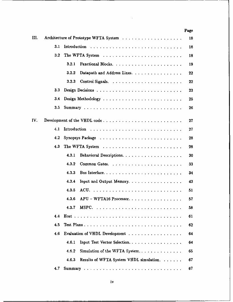
Table of Contents
Page
List of Figures .......... ...................................... viii
List of Tables .......... ....................................... xi
List of Abbreviations ............................................ xii
Abstract .................................................... xiii
1. Introduction .......... .................................... 1
1.1 Background.... ............................ 2
1.2 Problem Statement ................................. 4
1.3 Objectives ......... ............................... 4
1.4 Scope ........................................... 5
1.5 Approach ....................................... 6
1.5.1 Design of the VMEbus Interface ................... 6
1.5.2 Development of VHDL Code ...................... 7
1.5.3 Construction of the WFTA System ................. 8
1.5.4 Development of Host Software .................... 8
1.6 Materials and Equipment ............................ 9
1.7 Sequence of Presentation ........ ...................... 9
II. Literature Review ......... ................................ 12
2.1 Introduction ......... ............................. 12
2.2 AFIT Research .................................... 12
2.3 Other WFTA Efforts ................................. 16
2.4 Summary ......... ............................... 17
IIIa.
Page
III. Architecture of Prototype WFTA System ......................... 18
3.1 Introduction ......... ............................. 18
3.2 The WFTA System .............. .... ................ 18
3.2.1 Functional Blocks ............................. 19
3.2.2 Datapath and Address Lines ...................... 22
3.2.3 Control Signals .............................. 22
3.3 Design Decisions ........ ........................... 23
3.4 Design Methodology ................................. 25
3.5 Summary ......... ............................... 26
IV. Development of the VHDL code ................................ 27
4.1 Introduction ......... ............................. 27
4.2 Synopsys Package ........ .......................... 28
4.3 The WFTA System ........ ......................... 28
4.3.1 Behavioral Descriptions ......................... 30
4.3.2 Common Gates .............................. 33
4.3.3 Bus Interface ................................ 34
4.3.4 Input and Output Memory. ..................... 43
4.3.5 ACU ..................................... 51
4.3.6 APU - WFTA16 Processor ...................... 57
4.3.7 MSPC .................................... 58
4.4 Host .......... .................................. 61
4.5 Test Plans ....................................... 62
4.6 Evaluation of VHDL Development ...................... 64
4.6.1 Input Test Vector Selection ...................... 64
4.6.2 Simulation of the WFTA System ................... 65
4.6.3 Results of WFTA System VHDL simulation ....... ... 67
4.7 Summary ........................................ 67
iv
Page
V. Construction of the WFTA System .............................. 68
5.1 Introduction ......... ............................. 68
5.2 Resources ......... ............................... 69
5.2.1 Equipment and Tools .......................... 69
5.2.2 Integrated Circuits ........................... 70
5.2.3 Other Parts ................................. 71
5.3 Partitioning of Functional Blocks ........................ 73
5.4 Construction Methodology and Testing ................... 74
5.5 Specific Problems ................................... 76
5.5.1 Interface to Host ............................. 76
5.5.2 Parts ..................................... 76
5.5.3 Testing .................................... 77
5.6 Evaluation of Construction ....... ..................... 77
5.7 Summary ......... ............................... 77
VI. Development of the Host Driver Code ....... ..................... 78
6.1 Introduction ......... ............................. 78
6.2 Compilation, Download, and Run Procedures ............... 79
6.3 Pseudocode for the Host Driver Program .................. 79
6.4 Data Flow Diagram for Host Driver Code ................. 81
6.5 Coding and Memory Map ............................. 82
6.6 Testing and Evaluation of Host Driver Program Development . . 84
6.7 Summary ......... ............................... 84
VII. Conclusions and Recommendations .............................. 85
7.1 Introduction ......... ............................. 85
7.2 Conclusions ...................................... 85
7.2.1 Validation of WFTA System Design ................ 85
v
Page
7.2.2 Continued Work in the WFTA System .............. 86
7.3 Recommendations ........ .......................... 86
7.3.1 Further VLSI Work ........................... 87
7.3.2 Asynchronous Signals .......................... 87
7.3.3 Different Host ............................... 88
7.3.4 Behaviorial Descriptions of Chips ................. 88
7.3.5 Supply of Resources ........................... 88
7.4 Lessons Learned ........ ........................... 89
7.4.1 Scheduling of Construction ...................... 89
7.4.2 Construction Methodology ...................... 89
7.4.3 Ordering of Parts ............................. 89
7.5 Summary ......... ............................... 90
Appendix A. Schematics for Subcomponents ......................... 91
Appendix B. Timing Diagrams for Functional Blocks ................... 106
Appendix C. Test Vectors for 1 Hz Sine Wave ........................ 118
Appendix D. Timing Diagrams for WFTA System ..................... 122
Appendix E. Major Distributors and Suppliers of Parts ................. 130
Appendix F. Chip Layouts for the VMEbus Boards ................... 132
Appendix G. Compilation, Download, and Run Procedures for Host Driver Code 138
G.1 Compilation Procedure ....... ....................... 138
G.2 Download Procedure ................................ 139
G.3 Run Procedure ........ ............................ 141
Appendix H. Changes to Pseudocode for Sustained Operations ............ 143
vi
Page
Appendix I. Host Driver Code Listing ............................. 145
Appendix J. Operator's Manual for the 16-point WFTA System .......... 147
J.1 Hardware ........ ............................... 147
J.1.1 Setup .................................... 147
J.1.2 WFTA Address Change ........................ 147
J.2 Software ........................................ 148
J.2.1 Host Driver Code and Data ...................... 148
J.2.2 Running the Host Driver Program ................. 152
J.2.3 Reading the Output Data ....................... 152
3.3 Problems in Operator's Manual ........................ 152
Appendix K. VHDL Code and Schematic Listing ...................... 153
References .......... ......................................... 154
Vita ............. ............................................ 157
vii
List of Figures
Figure Page
1. Simple Diagram of WFTA Architecture .......................... 3
2. Simple Diagram of WFTA Prototype Architecture ................... 5
3. Initial 1985 WFTA Architecture ........ ........................ 13
4. Reconfigurable WFTA Architecture ....... ...................... 15
5. Prototype WFTA System Architecture ....... .................... 20
6. WFTA System Architecture ........ .......................... 29
7. Memory Mapping for WFTA Prototype System .................... 35
8. Bus Interface Schematic ..................................... 37
9. Data Format for Control Word ........ ......................... 39
10. Data Format for Output Word ........ ......................... 40
11. Input Memory (MEMIN Component) ........................... 45
12. Output Memory (MEM.OUT Component) ....... .................. 46
13. Arithmetic Control Unit ......... ............................ 53
14. State Diagram for Minimal SPC ........ ........................ 60
15. Host-WFTA Relationship .................................... 61
16. Partitioning and Interconnect Signals ....... ..................... 74
17. Pseudocode for the Host Driver Program ......................... 80
18. Context Diagram for the Host Driver Program ...................... 82
19. Level 1 DFD for Host Driver Program ........................... 83
20. Memory Mapping for Host Driver Code and Data ................... 83
21. Input Section Schematic-VMEbus Interface ........................ 92
22. Control Section Schematic-VMEbus Interface ...... ................ 93
23. Output Section Schematic-VMEbus Interface ...................... 94
24. DEMUXI Block Schematic-Input Memory ....... .................. 95
25. DEMUXla Block Schematic-Output Memory ...... ................ 96
viii
Figure Page
26. DEMUX2 Block Schematic-Input and Output Memory ............... 97
27. DEMUX3 Block Schematic-Input and Output Memory ............... 98
28. MEM-MCM6264 Block Schematic-Input and Output Memory ........... 99
29. MUX2 Block Schematic-Input Memory .......................... 100
30. MUX2a Block Schematic-Input Memory ...... ................... 101
31. ACUINIT Block Schematic-ACU ............................. 102
32. ACUADD Block Schematic-ACU ............................. 103
33. ACUCOUNTER Block Schematic-ACU ......................... 104
34. ACUADD1 Block Schematic-ACU ....... ...................... 105
35. Timing Diagram-Input Section ................................ 107
36. Timing Diagram-Control Section(#1) ........................... 108
37. Timing Diagram-Control Section(#2) ........................... 109
38. Timing Diagram-Output Section(#1) ........................... 110
39. Timing Diagram-Output Section(#2) .......................... .111
40. Timing Diagram-Input Memory ............................... 112
41. Timing Diagram-Output Memory .............................. 113
42. Timing Diagram-ACU(#1) .................................. 114
43. Timing Diagram-ACU(#2) .................................. 115
44. Timing Diagram-MSPC ..................................... 116
45. Timing Diagram-WFTA System(#1) ....... ..................... 123
46. Timing Diagram-WFTA System(#2) ........................... 124
47. Timing Diagram-WFTA System(#3) ........................... 125
48. Timing Diagram-WFTA System(#4) ..................... 126
49. Timing Diagram-WFTA System(#5) ..................... 127
50. Timing Diagram-WFTA System(#6) ..................... 128
51. Timing Diagram-WFTA System(#7) ..................... 129
52. Layout of VME Board # 1 ........................... 133
ix
Figure Page
53. Layout of VME Board # 2 ........ ........................... 135
54. Signal Mapping of 50-Pin Interconnect Cable ...................... 137
55. Pseudocode for a Sustainable Host Driver Program ................. 144
56. Hardware Setup ......... ................................. 148
x
List of Tables
Tab.e Page
1. Integrated Circuits and Behavioral Descriptions ..... ............... 31
2. Instantiated Propagation Delays for Common Gates .................. 34
3. Decoding for WFTA Components ....... ....................... 36
4. Common 1, AEbus Signals Interfaced to the WFTA ..... ............. 39
5. Test Benches ......... ................................... 63
6. Integrated Circuit Requirements with Functional Blocks ............... 71
7. MSPC Timing Table ....................................... 117
8. Real Input Test Vectors for a 1 Hz Sine Wave ...... ................ 119
9. Expected and Actual Real Output Test Vectors for a 1 Hz Sine Wave . . . 120
10. Expected and Actual Imaginary Output Test Vectors for a 1 Hz Sine Wave 121
11. Integrated Circuits used on VME Board # 1 ...................... 134
12. Integrated Circuits used on VME Board # 2 ...................... 136
xi
List of Abbreviations
Symbol Page
digital signal processing (DSP) ................................... 1
Very large scale integration (VLSI) ............................... 1
Discrete Fourier Transform (DFT) ................................. 1
Air Force Institute of Technology (AFIT) ............................ 1
Winograd Fourier Transform Algorithm (WFTA) ..................... 1
Fast Fourier Transforms (FFT) ................................... 2
Prime Factoring Algorithm (PFA) ................................. 3
application-specific integrated circuits (ASIC) ........................ 3
Very High Speed Integrated Circuit (VHSIC) Hardware Description Language
(VHDL) .............................................. 4
computer-aided design (CAD) .................................. 7
Error-Correction Coding (ECC) .................................. 14
Arithmetic Processing Unit (APU) ................................ 16
Arithmetic Control Unit (ACU) .................................. 16
Small PFA Controller (SPC) .................................... 16
Minimal Small PFA Controller (MSPC) ............................ 19
signal-to-noise ratio (SNR) ..................................... 24
Simulation Graphical Environment (SGE) ............................ 28
Multi-Valued Logic-7 levels (MVL7) .............................. 28
finite state machine (FSM) ..................................... 59
Transistor- Transistor- Logic (TTL) ................................ 71
programmable gate array (PGA) ................................. 72
dual in-line package (DIP) ..................................... 73
data flow diagram (DFD) ...................................... 81
xii
AFIT/GCE/ENG/92D-05
Abstract
Since 1985, the Air Force Institute of Technology has pursued a project to develop
a 4080-point Discrete Fourier Transform processor using the Winograd Fourier Transform
Algorithm (WFTA) and Good-Thomas Prime Factoring Algorithm (PFA). In the first
attempt to build a working system, this research effort designed and constructed, in part,
a modified single processor architecture in order to demonstrate the proof of concept of
the WFTA system design. This prototype architecture is simpler in implementation but
uses the same priniciples and procedures as those of the 4080-point WFTA design. The
design developed in this thesis was validated using the Very High-Speed Integrated Circuit
Hardware Description Language (VHDL) to simulate its operation. A partial construction
of the design was built and tested verifying the VHDL results.
xiii
DESIGN AND DEVELOPMENT
OF A HIGH-SPEED WINOGRAD
FAST FOURIER TRANSFORM
PROCESSOR BOARD
L Introduction
In both commercial and military arenas, digital signal processing (DSP) has become
a rapidly expanding area of interest. With this rising interest there continues to be a need
for higher performance digital signal processors that are faster and able to handle larger
amounts of data. Very large scale integration (VLSI) has provided the means by which
faster calculations and higher throughput can be realizable with these DSP processors.
Algorithms normally implemented through software can be made faster by directly imple-
menting them on integrated circuits. This makes the integrated circuit specific in its use
but generally faster than those used in general purpose machines.
One of the many DSP tools is the Discrete Fourier Transform (DFT) which is a
mathematical tool that can be used to filter noise from a particular signal frequency [1].
This particular use of the DFT has direct applications in radar processing. One possible
implementation is in the nose of "smart" ordnance where a fast DFT could be calculated
to screen out the noise generated by the enemy or environment [2].
This thesis effort supported the ongoing project at the Air Force Institute of Tech-
nology (AFIT) to implement the Winograd Fourier Transform Algorithm (WFTA) in
hardware. One of the processors which implements this algorithm is near completion but
a system configuration to install that processor has not yet been implemented. This thesis
effort demonstrates that chip in a system-level configuration and verifies that this fast
means of DFT calculation is both realizable and practical.
I
1.1 Background
The Fourier transform has been used for decades as a mathematical tool by electrical
engineers in the analysis of analog signals. The algorithm takes real physical processes de-
scribed in the time domain and "transforms" them into the frequency domain [3]. However,
the Fourier Transform only works on continuous signals and a different mathematical tool
is necessary for digital (discrete) signals. The Discrete Fourier Transform (DFT) is an ap-
proximation of the Fourier transform where "samples of the continuous Fourier transform
are evaluated numerically by using an approximation to the transformation integral." [4].
The DFT can be used on digital signals because of its discrete nature. Further, by in-
creasing the numbers of samples, closer approximations to the Fourier transform can be
realized.
However, the main problem with calculating DFT's using the straight summation
definition is that their calculation is computationally intensive. In fact, the complexity
of the Discrete Fourier Transform is an O(N 2 ) process [3]. In answer to this problem of
computational cost, many people have developed a class of algorithms called Fast Fourier
Transforms (FFT) . The FFT is a method for efficiently computing the DFT of a time
series [51. The Discrete Fourier Transform can, in fact, be computed in O(Nlog 2N) oper-
ations using FFT algorithms [3]. These FFT algorithms represent a significant reduction
in the computational complexity of the DFT, especially for larger N. There are many FFT
approaches that can be found in the literature, like the Cooley-Tukey FFT algorithm and
the base-4 FFT algorithm [3].
In his short paper, Schmuel Winograd develops a FFT algorithm which does not
decrease the complexity of the DFT calculation but does, however, decrease the number
of multiplications [6]. This reduction in the multiplications has important consequences in
the world of VLSI and chip design, because fewer multiplications translates into increased
speed and higher throughput. For this reason, the Winograd Fourier Transform Algorithm
(WFTA) is the theoretical basis for the research effort here at the Air Force Institute
of Technology. This effort has been to develop and build a specific co-processor which
implements the Winograd Fast Fourier Transform algorithm in hardware on a single chip
or suite of chips.
2
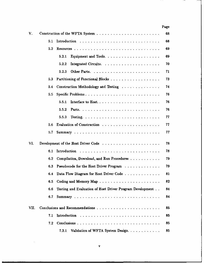
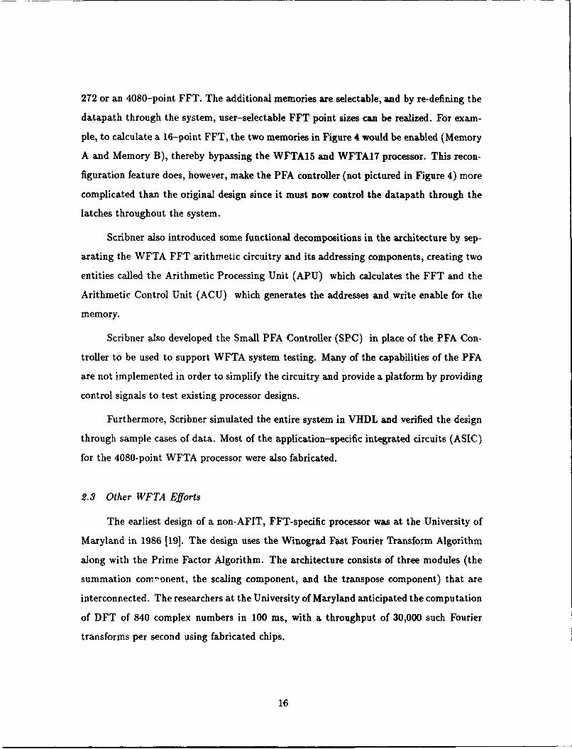
PFAController
aIn Data Out(from host) Control lines (to host)(•orr~to host)(tho)
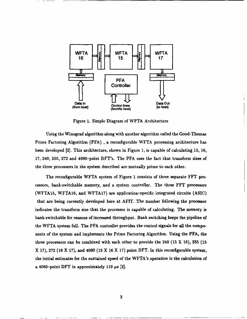
Figure 1. Simple Diagram of WFTA Architecture
Using the Winograd algorithm along with another algorithm called the Good-Thomas
Prime Factoring Algorithm (PFA) , a reconfigurable WFTA processing architecture has
been developed [2]. This architecture, shown in Figure 1, is capable of calculating 15, 16,
17, 240, 255, 272 and 4080-point DFT's. The PFA uses the fact that transform sizes of
the three processors in the system described are mutually prime to each other.
The reconfigurable WFTA system of Figure 1 consists of three separate FFT pro-
cessors, bank-switchable memory, and a system controller. The three FFT processors
(WFTA15, WFTA16, and WFTA17) are application-specific integrated circuits (ASIC)
that are being currently developed here at AFIT. The number following the processor
indicates the transform size that the processor is capable of calculating. The memory is
bank-switchable for reasons of increased throughput. Bank switching keeps the pipeline of
the WFTA system full. The PFA controller provides the control signals for all the compo-
nents of the system and implements the Prime Factoring Algorithm. Using the PFA, the
three processors can be combined with each other to provide the 240 (15 X 16), 255 (15
X 17), 272 (16 X 17), and 4080 (15 X 16 X 17) point DFT. In this reconfigurable system,
the initial estimates for the sustained speed of the WFTA's operation is the calculation of
a 4080-point DFT in approximately 119 ps [2].
3
1.2 Problem Statement
There is a lack of a platform or system environment, including an interface to a
suitable host processor, for WFTA processor operation. This research was an effort to
design and build a working 16-point WFTA system that interfaces to the VMEbus standard
to demonstrate the proof of concept in the WFTA design developed at the Air Force
Institute of Technology.
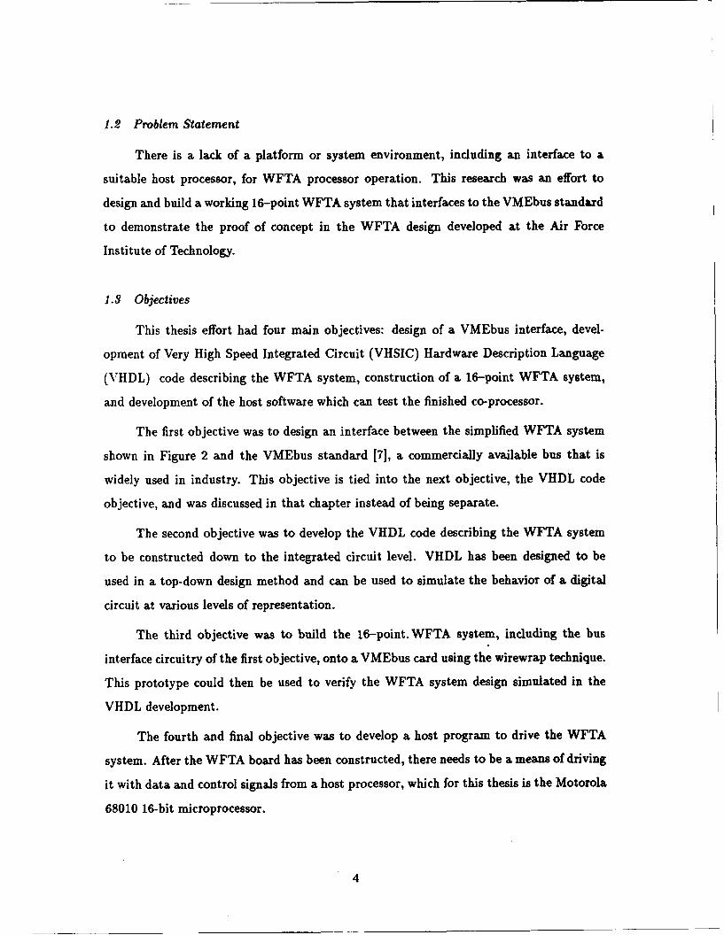
1.3 Objectives
This thesis effort had four main objectives: design of a VMEbus interface, devel-
opment of Very High Speed Integrated Circuit (VHSIC) Hardware Description Language
(VHDL) code describing the WFTA system, construction of a 16-point WFTA system,
and development of the host software which can test the finished co-processor.
The first objective was to design an interface between the simplified WFTA system
shown in Figure 2 and the VMEbus standard [7], a commercially available bus that is
widely used in industry. This objective is tied into the next objective, the VHDL code
objective, and was discussed in that chapter instead of being separate.
The second objective was to develop the VHDL code describing the WFTA system
to be constructed down to the integrated circuit level. VHDL has been designed to be
used in a top-down design method and can be used to simulate the behavior of a digital
circuit at various levels of representation.
The third objective was to build the 16-point. WFTA system, including the bus
interface circuitry of the first objective, onto a VMEbus card using the wirewrap technique.
This prototype could then be used to verify the WFTA system design simulated in the
VHDL development.
The fourth and final objective was to develop a host program to drive the WFTA
system. After the WFTA board has been constructed, there needs to be a means of driving
it with data and control signals from a host processor, which for this thesis is the Motorola
68010 16-bit microprocessor.
4
An ancillary objective implied by these specific ones above was to generate an opera-
tor's manual for the constructed WFTA system which will guide the operator as to proper
procedure and any particular considerations of the WFTA operation.
Documentation through these four objectives was stressed in order to provide follow-
on work and researchers a basis for the smoothest transition possible.
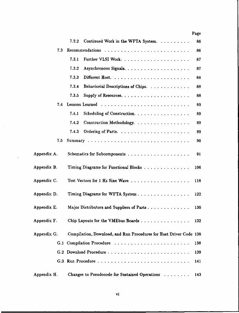
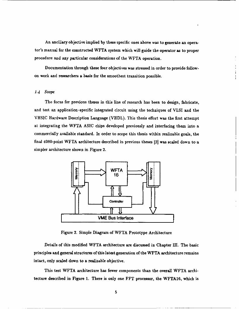
1.4 Scope
The focus for previous theses in this line of research has been to design, fabricate,
and test an application-specific integrated circuit using the techniques of VLSI and the
VHSIC Hardware Description Language (VHDL). This thesis effort was the first attempt
at integrating the WFTA ASIC chips developed previously and interfacing them into a
commercially available standard. In order to scope this thesis within realizable goals, the
final 4080-point WFTA architecture described in previous theses 12] was scaled down to a
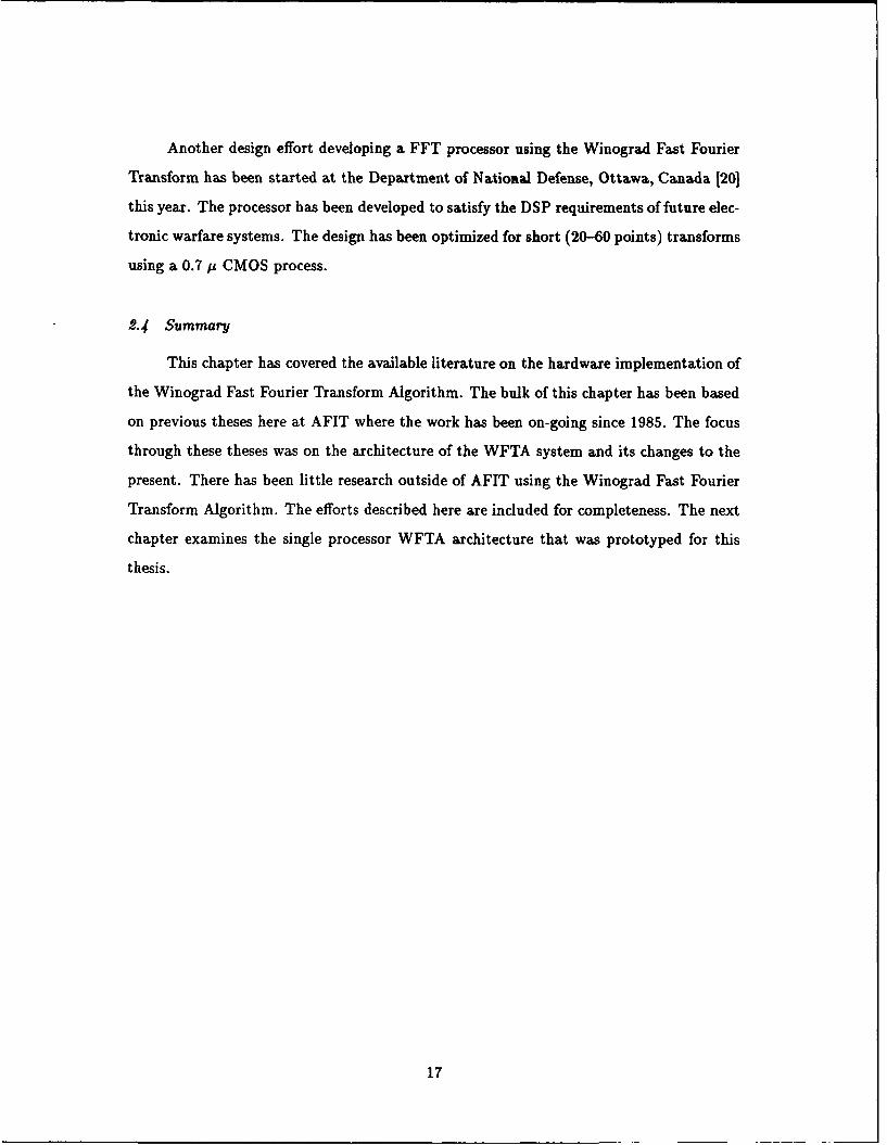
simpler architecture shown in Figure 2.
C ontroller
VME Bus Interface
Figure 2. Simple Diagram of WFTA Prototype Architecture
Details of this modified WFTA architecture are discussed in Chapter III. The basic
principles and general structures of this latest generation of the WFTA architecture remains
intact, only scaled down to a realizable objective.
This test WFTA architecture has fewer components than the overall WFTA archi-
tecture described in Figure 1. There is only one FFT processor, the WFTA16, which is
5
capable of calculating a 16-point DFT. The two memories are bank-switchable like in the
overall architecture and are similarly used to increase the throughput of the system. The
system controller here is different than the one used in the overall WFTA design since
it does not implement the Prime Factor Algorithm. This test architecture is limited to
calculating only one DFT, the 16-point DFT.
Due to resource problems and time, the degree of completion on the construction of
the WFTA system was also scoped to insure that whatever part of the system built could
be demonstrated.
1.5 Approach
Each one of the objectives described above entails a different approach. In all these
methodologies, there is a common thread of understanding. The future development of
WFTA systems must be taken into account whenever possible in order to simplify the
efforts of research that follow this thesis.
1.5.1 Design of the VMEbus Interface. The VMEbus standard [7] explicitly de-
sci.Ses the requirements of the VMEbus, and by using fundamental digital design prin-
ciples and heuristics, the interface between the WFTA system and the VMEbus can be
built modularly. The WFTA system is essentially a co-processor or, in other words, a slave
device waiting for the commands of the host processor. The WFTA system does not con-
tinuously operate and needs to be separated from the general operation of the VMEbus.
This communication requires an interface between the VMEbus and the WFTA with a
certain defined protocol. An example of one of the considerations for this interface is: How
does the host processor tell the WFTA system to begin processing? These considerations
along with others for this design are examined in detail in Chapter IV of this thesis.
There were no attempts to optimize the combinational logic of the design using
currently available optimization tools. Future researchers should review this design and
attempt to optimize the circuits whenever possible.
In short, the WFTA system cannot be directly connected to the VMEbus system.
This interface provides the means of communication between the WFTA system and the
6
host processor. Without an adequate VMEbus interface, the WFTA cannot be loaded,
told to operate, or have output read.
1.5.2 Development of VHDL Code. The use of VHDL is rapidly becoming com-
monplace in engineering circles. Using software to simulate a piece of hardware can save
thousands of man-hours in the design process for large systems. The secret to its success
is that the design can be built hierarchically from top to bottom (from a high block-level
representation to a gate-level representation). At each level, the description can be simu-
lated to demonstrate the correctness of the design. This thesis attempted to use VHDL in
this fashion. Starting from a high-level depiction of the WFTA system, each of the mod-
ules was implemented in VHDL. Within each module the behavioral description of the
module was replaced with the structural representation until the lowest-level behavioral
descriptions of the components were taken from the actual specifications of the chips used
in the construction of the WFTA system.
AFIT has recently acquired a software package produced by Synopsys, Incorporated
which includes a VHDL simulation system. This computer-aided design (CAD) tool uses
a graphical user interface which helps the designer to visualize the system through the
use of schematics. A number of attractive features of this software package were used for
this thesis. This Synopsys CAD tool was used heavily and extensively in the design and
development of the VHDL code for the WFTA system tested.
VHDL also provides a means of self-documentation for the design. Following the
hierarchical development of the design provides the reader with ample information on the
actual construction of the digital system. The VHDL cbde for this thesis also has comments
and headers in the code to help clarify the more difficult and possibly cryptic sections.
Again, development of the VHDL code was modular for ease of follow-on work in
this area of research. These future researchers should be able to add new descriptions or
augment the existing descriptions of components and simply "re-wire" the system for a
different implementation. The only components that should change from different config-
urations would be the controllers, which would get more complex as additional functions
are added with the larger point processors and larger configurations.
7
1.5.3 Construction of the WFTA System. As mentioned previously, the construc-
tion of the WFTA system described in Figure 2 is the main thrust of this thesis effort.
Using commercially available chips whenever possible, the WFTA prototype system is built
on two VME boards that slides into any VME backplane. Using the wire-wrap method of
construction, all the components were connected on one side of the VME cards. The only
ASIC chip used for this thesis was the WFTA16 FFT processor.
1.5.4 Development of Host Software. The host driver program is the program lo-
cated in the host that "drives" the WFTA system. This program was written in the C
programming language. Using a 68010 compiler, executable code is generated from the
host driver program and downloaded through a specified procedure to the host.
This host program loads the input memory bank with 16 points of real data (real
signals have no imaginary components) and tells the WFTA system controller to begin pro-
cessing. When the memory switches to receive the input data into the WFTA16 processor,
the host program continues to load as input the next set of points into the second memory
bank. Once the WFTA system controller indicates to the host that it has completed a set
of the data points, the host reads the output data (both real and imaginary parts) from the
output memory bank. Meanwhile, the WFTA16 has read in the new data and continues
calculating the DFT of the new data. The host driver program can then load a new set of
points into the input memory bank. This process continues until an end of the set of data
points is reached.
The host driver program was developed using sound and fundamental software engi-
neering principles, paying particular attention to the concept of modularity. Development
of the host driver program is discussed in Chapter VI. Subsequent thesis efforts in this
area of research will continue the step-wise progress toward the overall WFTA architecture
envisioned in Figure 1. The host driver program must be flexible enough to adapt to these
modifications without undue difficulty. The C language, with its ability to manipulate bits
at the machine level, was specifically chosen for this needed flexibility in the future devel-
opment of host driver software. Furthermore, the C language is a high-level programming
8
language, which makes it easier to maintain programs written in C rather than in assembly
language.
1.6 Materials and Equipment
The following list describes the major pieces of equipment and other resources that
were used to support this thesis effort.
1. AFIT VLSI/VHSIC Laboratory Sparc2 workstations
2. VME backplane
3. 68010 host processor card with a means of user interface
4. Synopsys VHDL simulation environment (Version 2.2)
5. Tools and equipment in the Digital Design Lab
6. 68010 Compiler
1.7 Sequence of Presentation
The following paragraphs of this section outline the order of presentation in this
thesis.
Chapter II documents the past efforts at AFIT in WFTA design and looks at other
implementations of FFT processors using the Winograd Fast Fourier Transform Algorithm
in the industrial and academic communities.
Chapter III presents the modified architecture of the WFTA system used in this
thesis. This is the first time this scaled-down architecture has been used, so a detailed ex-
amination of its structure is given before beginning the discussion of each of the objectives.
The next three chapters discuss each one of the objectives outlined in this chapter.
Chapter IV discusses the VHDL code development for the WFTA system. The chapter
begins with the development of the behavioral descriptions created and continues through
the final structural description of the WFTA system used.
9
Chapter V describes the modular construction of the WFTA design along with testing
procedures used to ensure proper operation. Specific problems and resources are addressed.
Chapter VI describes the development of the host processor code that was used in
the testing process.
Chapter VII discusses the conclusions of this research and recommendations for future
thesis cycles.
Appendix A contains the schematics created during the VHDL development for sub-
components of the WFTA system.
Appendix B contains timing diagrams generated from VHDL test benchs showing
the interrelationships of significant signals in each of the major functional blocks.
Appendix C contains the test vectors (both input and output) used in the system-
level VHDL simulation to verify system design.
Appendix D contains the timing diagrams generated from the VHDL test bench
simulation for the entire WFTA system. These timing diagrams in conjunction with the
test vectors in Appendix C were used to verify the WFTA system design.
Appendix E is a listing of nationwide distributors with phone numbers that provided
supplies for the construction phase of this thesis.
Appendix F is a layout of the two VMEbus boards on which the WFTA system was
constructed with chip reference numbers and chip identifications.
Appendix G is the description of the procedures developed during this thesis to
compile, download, and run the host driver program.
Appendix H contains the necessary additions to change the pseudocode of the host
driver program from single FFT operation to multiple FFT operation.
Appendix I is a listing of the host driver program developed for driving the WFTA
system.
Appendix J is a short operator's manual that can be used to guide the user in the use
and peculiarities of the WFTA prototype system. It provides all the necessary instructions
10
to operate the WFTA system. This appendix was meant to be detached from the thesis
and used as a handy guide with the WFTA system developed.
Appendix K is the listing of all the VHDL code, to include testbenches, and the
Synopsys generated schematics discussed in the thesis.
11
IH. Literature Review
2.1 Introduction
Research on the WFTA at the Air Force Institute of Technology has been on-going
since 1985. This is the latest thesis in along line of research conducted in the WFTA project
area by master's candidates in the Electrical and Computer Engineering Department.
Consequently, the bulk of literature available and the bulk of this search is from the work
of past theses at AFIT.
The focus of this literature search was on the architecture of the WFTA system and
how it has changed from the original design of 1985. Outside of the research at AFIT,
there has been little work in implementing the Winograd Fast Fourier Transform Algorithm
in hardware, but there have been some attempts. These outside efforts are included for
completeness.
2.2 AFIT Research
The WFTA project at AFIT began back in 1985 when Linderman, director of AFIT
VLSI Research Group, introduced the idea of a hardware implementation of the Winograd
Fast Fourier Transform Algorithm [8]. That year, four AFIT students started the process
of WFTA development with their thesis efforts. Each one worked in a specific area; Taylor
in WFTA system development; Coutee in VLSI arithmetic circuitry; Rossbach in VLSI
control circuitry; and Collins in VLSI circuit simulation.
Coutee developed the arithmetic circuitry necessary for the processing of data going
through one of the FFT processors, the WFTA16 architecture. Using the techniques of
VLSI design, Coutee designed a chip that performed the arithmetic calculations of the
DFT using the Winograd Fast Fourier Transform algorithm [9].
Rossbach designed the control circuitry for the initial WFTA effort. He designed two
circuits to control the arithmetic and address generation circuitry for the WFTA processor.
A notable byproduct of Rossbach's thesis was that he developed a XROM compiler, which
automatically generated a layout of the XROM Address Generator circuit discussed in his
thesis [10].
12
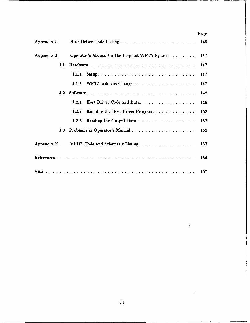
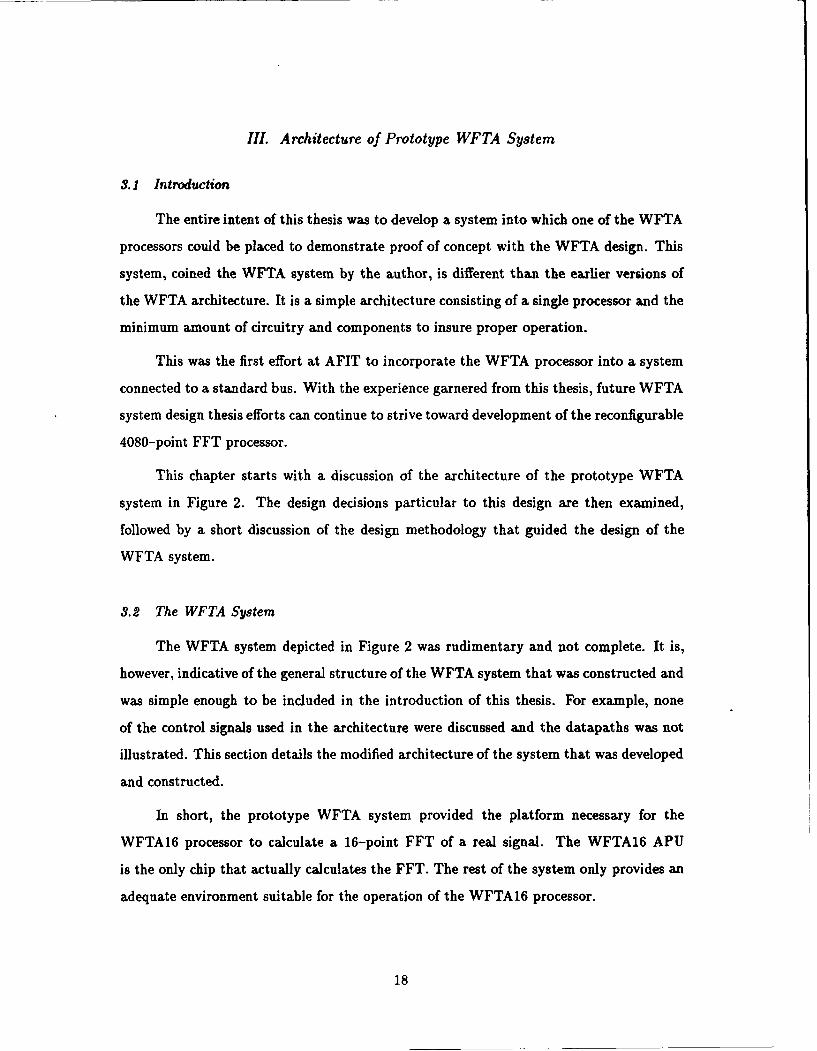
HOST
PFA Controller
MMemry MmyMr
Controlte Controller Contw owroler
, - Cj C, ccC~c
Input Memory Memory 1 Memory 2 Output Me&moy
Figure 3. Initial 1985 WFTA Architecture
The third AFIT student from that 1985 group was Collins, who developed a simu-
lation of the data flow in the WFTA-16 processor using the C programming language. He
also started the VHDL descriptions of certain sections of the WFTA-16 [11].
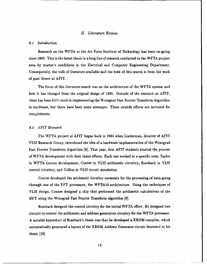
The last of those four students was Taylor, who developed a detailed description of
the WFTA algorithm as it applies to the system-level design. The layout or architecture
for the first WFTA system is found in his thesis, and Figure 3 is a re-creation of that layout
for the 4080-point processor. Taylor also provided the link between theory and hardware
by verifying the algorithm's accuracy with computer simulations. The design required
three WFTA processors (WFTA-15, WFTA-16, and WFTA-17), a PFA controller, and
intermediate memories. The points of data are pipelined through the three processors
according to the Prime Factor Algorithm to increase throughput of the system [81.
The memory was dual-ported (takes both a read and write address) with two separate
banks of memory. The memory controllor controlled the data flow of the pipeline depending
on control signals from the interface processor or PFA controller. Write enable signals
and addresses were generated by the WFTA processor control circuitry. Fault detection
13
was built into this system with Error-Correction Coding (ECC) circuitry and watchdog
processors. The ECC was built into the memory, and along with parity checks, the WFTA
processors would provide continuous checking of (corrected) data. The design called for two
additional watchdog processors which were redundant, inactive processors that calculate
the FFT at the same time and compare results to the active processor. If a difference is
detected, the system recovered by alerting the PFA controller that a possible error has
occurred. The PFA controller decided which output is allowed to continue to the next
stage of the pipeline through voting circuitry between the three processors.
In the following year, 1986, hardware implementation began with the three AFIT
students assigned to the WFTA project. These theses dealt with operational issues, but
made no significant changes to the system architecture. Shepard continued work on the
first implementation of the WFTA16 processor in silicon [12].
Hedrick was the second student from the 1986 group and worked in the design of the
PFA controller as well as custom memory chips and memory controllers to be used in the
WFTA system [13].
The third thesis student of the 1986 group was Cooper, who up-dated the VHDL
description of the WFTA16 processor, incorporating the changes from the 1985 design [14].
In 1987, Hauser continued work in the design and implementation of the intercon-
necting memory modules and the PFA controller [15]. Hauser designed the ECC circuitry
discussed earlier. Again there were no significant changes in this thesis to the architecture
of the WFTA system.
In 1988, Tillie and Comtois designed the WFTA17 processor as a class project [16].
They modified existing macrocells used for the 16-point processor and designed new macro-
cells unique to the WFTA17 processor.
The next thesis was Pavick's, who in 1989 performed testing of the WFTA16 pro-
cessors built earlier and re-designed cells in the processor [16]. The system architecture
remained unaffected.
Baker used VHDL to validate the 4080-point WFTA processor design in 1990 [17].
He succeeded in developing behavioral descriptions of the three WFTA processors and
14
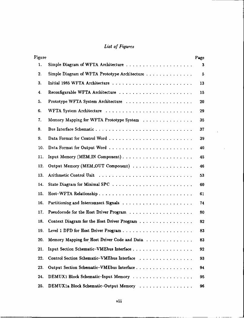
HOST
DATA IN PATH
Figure 4. Reconfigurable WFTA Architecture
provided the nucleus for future VHDL work in the WFTA processors. The 4080-point
design used here is essentially the same architecture developed in 1985.
Also in 1990, Sommer focused on the development of the WFTA cell library and
the design of the WFTA15 processor [18]. Again, there were no major changes to the
architecture of the WFTA system.
From the auspicious start of the WFTA project in 1985, there has been steady
progress toward the realization of a 4080-point WFTA processor every year. However, up
to last year, the basic architecture has remained faithful to the original design.
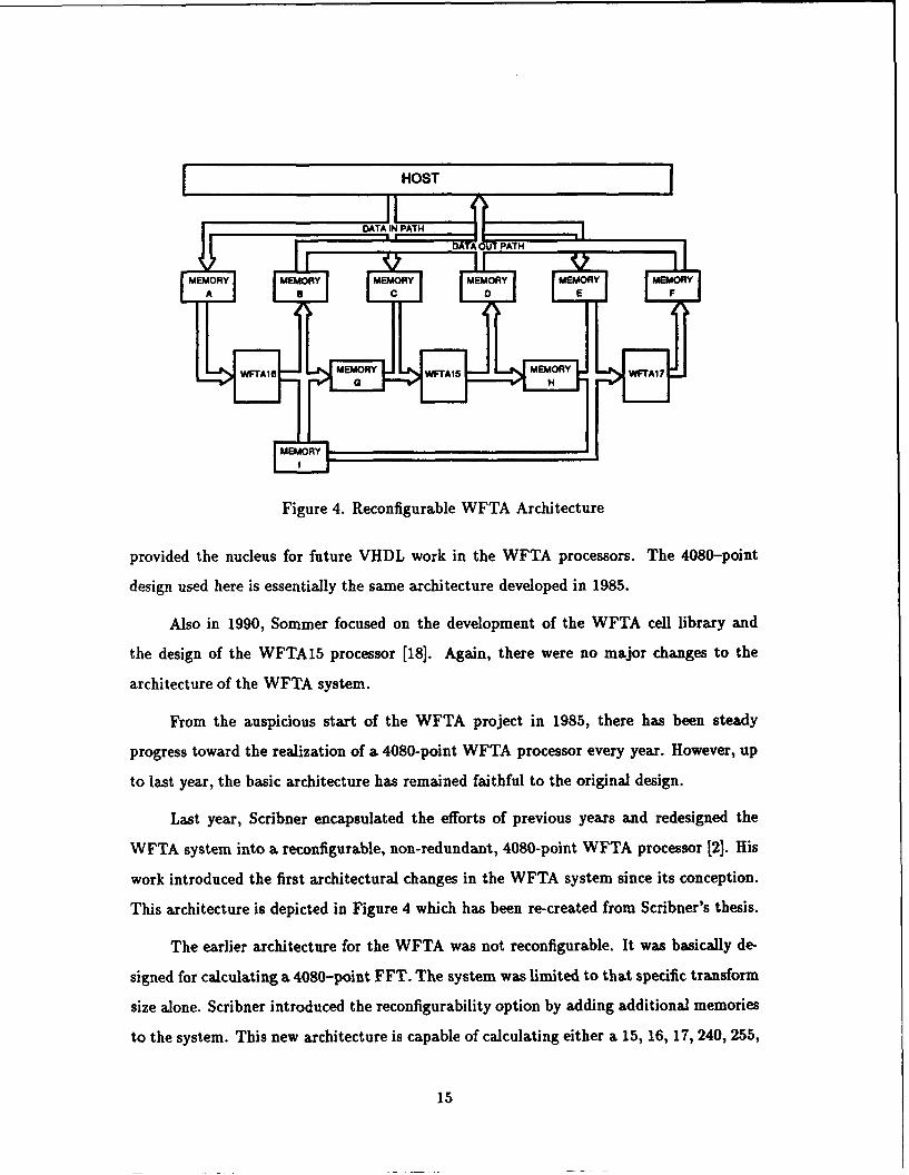
Last year, Scribner encapsulated the efforts of previous years and redesigned the
WFTA system into a reconfigurable, non-redundant, 4080-point WFTA processor 121. His
work introduced the first architectural changes in the WFTA system since its conception.
This architecture is depicted in Figure 4 which has been re-created from Scribner's thesis.
The earlier architecture for the WFTA was not reconfigurable. It was basically de-
signed for calculating a 4080-point FFT. The system was limited to that specific transform
size alone. Scribner introduced the reconfigurability option by adding additional memories
to the system. This new architecture is capable of calculating either a 15, 16, 17, 240, 255,
15
272 or an 4080-point FFT. The additional memories are selectable, and by re-defining the
datapath through the system, user-selectable FFT point sizes can be realized. For exam-
ple, to calculate a 16-point FFT, the two memories in Figure 4 would be enabled (Memory
A and Memory B), thereby bypassing the WFTA15 and WFTA17 processor. This recon-
figuration feature does, however, make the PFA controller (not pictured in Figure 4) more
complicated than the original design since it must now control the datapath through the
latches throughout the system.
Scribner also introduced some functional decompositions in the architecture by sep-
arating the WFTA FFT arithmetic circuitry and its addressing components, creating two
entities called the Arithmetic Processing Unit (APU) which calculates the FFT and the
Arithmetic Control Unit (ACU) which generates the addresses and write enable for the
memory.
Scribner also developed the Small PFA Controller (SPC) in place of the PFA Con-
troller to be used to support WFTA system testing. Many of the capabilities of the PFA
are not implemented in order to simplify the circuitry and provide a platform by providing
control signals to test existing processor designs.
Furthermore, Scribner simulated the entire system in VHDL and verified the design
through sample cases of data. Most of the application-specific integrated circuits (ASIC)
for the 4080-point WFTA processor were also fabricated.
2.3 Other WFTA Efforts
The earliest design of a non-AFIT, FFT-specific processor was at the University of
Maryland in 1986 [19]. The design uses the Winograd Fast Fourier Transform Algorithm
along with the Prime Factor Algorithm. The architecture consists of three modules (the
summation coirnonent, the scaling component, and the transpose component) that are
interconnected. The researchers at the University of Maryland anticipated the computation
of DFT of 840 complex numbers in 100 ms, with a throughput of 30,000 such Fourier
transforms per second using fabricated chips.
16
Another design effort developing a FFT processor using the Winograd Fast Fourier
Transform has been started at the Department of National Defense, Ottawa, Canada 120]this year. The processor has been developed to satisfy the DSP requirements of future elec-
tronic warfare systems. The design has been optimized for short (20-60 points) transforms
using a 0.7 p CMOS process.
2.4 Summary
This chapter has covered the available literature on the hardware implementation of
the Winograd Fast Fourier Transform Algorithm. The bulk of this chapter has been based
on previous theses here at AFIT where the work has been on-going since 1985. The focus
through these theses was on the architecture of the WFTA system and its changes to the
present. There has been little research outside of AFIT using the Winograd Fast Fourier
Transform Algorithm. The efforts described here are included for completeness. The next
chapter examines the single processor WFTA architecture that was prototyped for this
thesis.
17
IHL Architecture of Prototype WFTA System
3.1 Introduction
The entire intent of this thesis was to develop a system into which one of the WFTA
processors could be placed to demonstrate proof of concept with the WFTA design. This
system, coined the WFTA system by the author, is different than the earlier versions of
the WFTA architecture. It is a simple architecture consisting of a single processor and the
minimum amount of circuitry and components to insure proper operation.
This was the first effort at AFIT to incorporate the WFTA processor into a system
connected to a standard bus. With the experience garnered from this thesis, future WFTA
system design thesis efforts can continue to strive toward development of the reconfigurable
4080-point FFT processor.
This chapter starts with a discussion of the architecture of the prototype WFTA
system in Figure 2. The design decisions particular to this design are then examined,
followed by a short discussion of the design methodology that guided the design of the
WFTA system.
3.2 The WFTA System
The WFTA system depicted in Figure 2 was rudimentary and not complete. It is,
however, indicative of the general structure of the WFTA system that was constructed and
was simple enough to be included in the introduction of this thesis. For example, none
of the control signals used in the architecture were discussed and the datapaths was not
illustrated. This section details the modified architecture of the system that was developed
and constructed.
In short, the prototype WFTA system provided the platform necessary for the
WFTA16 processor to calculate a 16-point FFT of a real signal. The WFTA16 APU
is the only chip that actually calculates the FFT. The rest of the system only provides an
adequate environment suitable for the operation of the WFTA16 processor.
18
This single processor architecture design could be used with any of the other WFTA
processors with a re-design of the arithmetic control unit (ACU). The ACU for this thesis
is tailored for the WFTA16 processor latency time and the WFTA16 addressing require-
ments. However, the rest of the design is compatible with either the WFTA15 or WFTA17
processors.
The WFTA system described by Figure 5 is more complete, showing all the functional
blocks, the datapaths, and the important control signals designed in this thesis. Figure 5
is a simpler system and many of the signals discussed by Scribner [2] are not supported.
Simplicity in design was an important objective in order to develop a complete platform
during this thesis cycle. Signals related to more advanced features of the WFTA are left
for future researchers to implement in a system configuration. Only the major control
signals that were actually used for this design are depicted in Figure 5.
The rest of this section is a general discussion of the architecture used for this the-
sis. The major functional blocks are described in general detail. The datapath through
the system is highlighted. Finally, the important control signals used are identified and
described.
3.2.1 Functional Blocks. There are six major logical functional blocks used in this
design: the VMEbus interface, the input memory, the Arithmetic Processing Unit (APU),
the Arithmetic Control Unit (ACU), the Minimal Small PFA Controller (MSPC) , and the
output memory. Each of these blocks are discussed below with a general description of the
function. Specific design details are left for Chapter IV on VHDL development.
The VMEbus is an asynchronous bus directly suited for the Motorola 68010 micro-
processor. The VMEbus interface provides the WFTA system with the necessary interface
between the VMEbus and the WFTA system. The host processor accesses logic within
this block for all communications with the WFTA system. This communication includes
writing data to the input memory, reading data from the output memory, instructing the
MSPC to begin operation, and receiving notification when the MSPC is completed with a
FFT calculation.
19
EE -
* I I2 E
"" 0
~~I
j•i i ,
-U 0- C
" ( 10 .. ...0' ... 0
<o
U-.I
~CU O
00
Figure 5. Prototype WFTA System Architecture
20
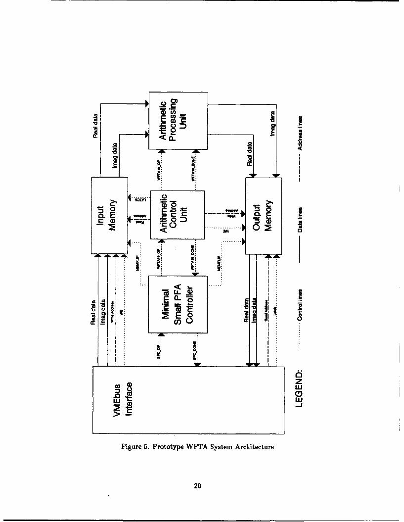
The input memory actually consists of two memories (real and imaginary), each
containing two switchable banks of memory. This bank-switched architecture is used in
order to increase the throughput of the device. The host writes to the one bank of memory
while the APU reads from the other bank of memory. The two address ports on this
memory allow simultaneous access to both banks of memory, which is necessary in order
to keep the WFTA system pipeline full. Additionally, the input memory is even-byte
addressable from the VMEbus. The host can only write to the input memory, it cannot
read back any of the data.
The Arithmetic Processing Unit (APU) is an application-specific integrated circuit
designed at AFIT that reads in data from the input memory, calculates the FFT, and
outputs the transformed data to the output memory.
The Arithmetic Control Unit (ACU) works in conjunction with the APU in order to
read and write data to and from the input and output memories. The ACU generates the
addresses for the input memory and output memory as well as a write enable pulse for the
output memory at the correct time. The timing between the ACU and APU are critical
and must be synchronized for the input and output of data to and from the APU.
The Minimal Small PFA Controller (MSPC) is the main controller for the entire
WFTA system, providing control signals to the system to ensure smooth and proper flow
of data through the system. Depending on the input signals, this controller transitions
through its states with changes in the corresponding output. This controller was devel-
oped specifically for this thesis and minimizes the number of control signals necessary
for complete system implementation. The detailed design of the MSPC is discussed in
Chapter IV.
The output memory, like the input memory, consists of two memories (real and
imaginary) each containing two banks of memory. However, the host reads from one bank
of memory while the APU writes to the other. Like the input memory, the output memory
is also even-byte addressable from the VMEbus. Additionally, the host can only read from
the output memory and cannot write to the output data addresses.
21
3.2.2 Datapath and Address Lines. The datapath for the real and imaginary data
flows in a clockwise direction in Figure 5, as indicated by the arrows on the data lines.
The host writes to the input memory, at which point the ACU and APU reads this data
into the APU and calculates the FFT. The output of the APU is written to the output
memory with addresses and a write enable generated by the ACU. After alerting the host
that data is available in the output memory, the host can then read the calculated FFT
from the output memory.
There are two addresses which are fed into the memory blocks shown in Figure 5 with
directions indicated. There are two addresses because the two banks of memory can be
simultaneously accessed. In the input memory, the VMEbus interface provides the write
address and the ACU provides the read address. Thus, the host can write data to one of
the banks of input memory, while the ACU can read data from the other bank of memory.
Similarly, in the output memory, the ACU provides the write address and the read address
is given by the VMEbus interface. The ACU can write data to one of the banks of memory,
while the host can read the other bank.
The address lines coming from and going to the VMEbus interface are simply the
lower eight address line bits on the VMEbus. In this design only sixteen data points are
addressed, which requires only four addressing bits. The four additional bits allows for
future expansion to other incremental architectures.
3.2.3 Control Signals. The major control signals used in this architecture are high-
lighted in Figure 5 with the direction indicated by the arrow. Each of these major control
lines is covered in a short discussion below. The other control signals mentioned in the
reconfigurable system of [2] not covered in this section are not supported in the design and
are left for the future development of this system.
The following control signals are signals that already exist in the architecture dis-
cussed by Scribner [2]. The SPCOP signal going from the VMEbus interface to the MSPC
tells the MSPC to begin operations on the set of data in the appropriate bank of input
memory. The SPCDONE signal, which originates in the MSPC, goes to the VMEbus
interface to tell the host the FFT has been completed and the output memory is ready
22
to be read by the host. The MEMFLIP signal going to both the input and output mem-
ory from the MSPC controls which bank of memory is oriented towards the host or the
APU. The WFTA16-OP signal coming from the MSPC goes to both the ACU and the
APU to begin calculation of the FFT using the set of data in the input memory, while the
WFTA 16-DONE signal generated by the ACU tells the MSPC when the data from the
WFTA system has been written to the output memory. This WFTA16-DONE signal also
tells the APU to reset some of its internal counters to prepare for the next FFT calculation.
The remaining control signals discussed in this section are peculiar to the WFTA
architecture of this thesis. The two LATCH signals are present because of the design
of the two memories. The LATCH signal coming from the ACU to the input memory
controls a multiplexer in the memory used to latch data from the bank of memory indicated
by the MEMFLIP control signal, and to output that data to the APU. Similarly, the
LA TCH signal coming from the VMEbus interface to the output memory controls another
multiplexer used to latch data going to the VMEbus interface. Both these LATCH signals
are asserted after approximately 100 ns. This delay in assertion accounts for propagation
delays of integrated circuits in the memory associated with establishing the datapath, in
addition to the memory access times.
One control signal not pictured in Figure 5 is the CONTROL-CLEAR signal, which
clears the control register in the VMEbus interface that feeds into the MSPC. This signal
is used to terminate the SPCOP signal after six clock cycles before the MSPC transitions
to its next state. Without this signal, there is no input signal to the MSPC to hold it in
the proper FFT-completion state.
3.3 Design Decisions
Several design decisions were made prior to and during the development of the WFTA
system design. Since this system was to be prototyped in AFIT's digital logic lab, there
was a desire to minimize the total chip count and to reduce the system to the fewest number
of VME cards possible. There was also a consideration to keep the design complexity at a
minimum to try to assure a working prototype by the end of this thesis. These two factors,
23
minimization of chip count and minimization of design complexity, were the general basis
for the design decisions made during this thesis.
One design decision was to select the type of hoAt processor to be used in the pro-
totyping of this design. Since the datapath of the WFTA system is 24-bits, a 32-bit
microprocessor, like the Motorola 68020 or Intel 486, seems to be the logical choice. How-
ever, there was a problem with resources, and the only microprocessor available for the
chassis used was the 16-bit Motorola 68010.
Another design decision was to reduce the width of the datapath from 24 bits to 16
bits. The original WFTA design called for a 24-bit wide datapath to insure the designers of
the required signal-to-noise ratio (SNR) for the original design specifications. This created
a design problem. Even though the platform for this system is the VMEbus backplane,
which can at a maximum be configured for 32 bit operations, the host planned for use is
the 16-bit Motorola 68010. The additional eight bits would have made the bus interface
more complicated, as a single write or read from the memory would take two bus accesses
instead of one. There is also an increase in the number of chips for the WFTA system to
handle a 24-bit datapath (approximately 32 chips in the memories alone). With these two
disadvantages, the WFTA system was decreased to a 16-bit datapath, with the WFTA
system providing the parity bit that is needed for the APU. To be sure a 16-bit FFT
would have adequate accuracy and SNR, tests were conducted by Mehalic [21] to determine
whether the reduction of data would have an adverse effect on the FFT calculated by the
APU. The tests between 24 bits and 16 bits indicated that the difference between outputs
were insignificant for the accuracy of the WFTA.
Another design decision was to eliminate the imaginary input memory for the WFTA
system. There was a problem acquiring the memory chips, which only allowed enough chips
for seven of the eight banks of memory required by the system. This factor, coupled with
the desire to decrease the total number of chips for the design, made elimination of the
imaginary input memory viable. This decision is reasonable since the WFTA is currently
expected to calculate the FFT of real signals only, which means the imaginary component
of the signal is non-existent, or zero.
24
Another design decision involved the polling mode of operation used to determine
when the WFTA has completed calculating a FFT. The fastest mode of operation, es-
pecially with an asynchronous bus such as the VMEbus, would be an interrupt driven
system with the WFTA interrupting the host processor immediately when the WFTA was
completed. In this system, using the Motorola 68010 host microprocessor, the difference
between polling and interrupt operations is negligible because the host does nothing while
the WFTA is calculating the FFT. In another system where the host is busy with other
tasks, this difference is much more noticable. However, the addition of a interrupt handler
module to request and respond to the interrupt lines of the VMEbus would have added
many more chips to the design of the bus interface, and decreased available space on the
VME cards. Therefore, polling was used for this prototype.
Another design decision was designing this prototype platform for use with only one
of the WFTA processors, specifically the WFTA16 processor. The only difference between
a system with a WFTA15 or WFTA17 processor is the design of the ACU. There are
different FFT processing cycle times associated with these processors versus the WFTA16,
as well as a different number of addresses to be generated. Again, however, to completely
design a reconfigurable WFTA, the ACU that would be required to generate the correct
signals for either the WFTA15, WFTA16 or the WFTA17 processor. This design would
have again increased the total number of chips. Furthermore, AFIT is now directing
research efforts towards the WFTA16, as the total transistor count for the WFTA16 is less
than the WFTA15 or WFTA17. This makes a prototype designed for the WFTA16 alone
feasiable, and even desirable.
3.4 Design Methodology
The methodology used in design of this system was to functionally decompose the
design using a top-down design philosophy. This first level decomposition is essentially
completed with the architecture illustrated in Figure 5. The bus interface provides the
necessary interaction between the WFTA system and the VMEbus. The input memory
stores the 16 points of real data from the host and feeds it to the APU. The ACU provides
the addresses and write enable signal to the respective memories at the correct time. The
25
APU calculates the FFT and outputs this information to the output memory. The output
memory stores the FFT from the APU and waits for the host to access the transformed
data. Finally, the MSPC orchestrates this interchange, controlling all the components of
the WFTA system. The schematics, as well as structural VHDL, in Appendix K generated
during the VHDL development of Chapter IV of this thesis provide the necessary detail
for further levels of design decompositions.
3.5 Summaryj
This chapter has covered the modified WFTA system of this thesis. This simiplied
single processor architecture has not been developed in previous theses and was discussed
in this chapter. The architecture for this system was discussed in detail including the major
functional blocks, the data path and address lines, and the significant control signals. The
major design decisions made prior to construction were also included to provide a historical
background to the system design. Finally, the top-down design methodology used in this
thesis was briefly covered. The next chapter deals with the development of the VHDL code
that simulates the WFTA system.
26
IV. Development of the VHDL code
4.1 Introduction
One of the objectives of this thesis was to develop the VHDL code to accompany and
document the design of the WFTA system to the component level. This chapter discusses
the VHDL development for the simplified WFTA system shown in Figure 5. Along with this
VHDL development comes the natural discussion of the hardware design of this prototype
WFTA system. The only behavioral VHDL descriptions of this system are at the chip
level with the more abstract functional blocks, such as the input memory or the ACU,
composed of structural VHDL descriptions using the behavioral chip descriptions.
VHDL is a powerful language available to the VLSI design engineer that can be used
to simulate hardware systems prior to implementation or construction for verification of
design. VHDL is a standard hardware description language developed under the auspices
of the Department of Defense in order to manage the documentation of digital designs.
There are many advantages to VHDL, including its public availability and technological
independence [22]. One of the major benefits of VHDL is that the language takes timing
into account. VHDL was adopted as an IEEE standard in December of 1987 [23]. In fact,
the reason that VHDL is used in this thesis is to provide verification for the WFTA system
design of Figure 5. Before prototyping one chip to a VME board, the designer can be
reasonably assured that the design is correct with results from VHDL simulation.
This chapter starts with a short discussion of the Synopsys CAD tool used to de-
sign the WFTA system, followed by an examination of the WFTA system concentrating
on each one of the major functional blocks. The design described in this chapter repre-
sents the final design after all design iterations. The explanation of the test plans used
for individual testing and evaluation follows the comprehensive discussion of each of the
functional decompositions. The next section of this chapter concerns the host (described
in VHDL) used for the testing the entire system, followed with a discussion of the test
plans for the VHDL entities. Finally, the last section looks at an evaluation of the actual
results compared with the stated objective in Chapter I.
27
4.2 Synopsys Package
The VHDL analyzer and simulator used for this thesis was the Synopsys VHDL
System Simulator Core Programs, which include the Analyzer, Design Library, and Sim-
ulator [24]. The Analyzer compiles VHDL source files and produces an object file the
Simulator uses to simulate the system. A VHDL debugger program was also especially
useful in tracing down logical errors in the VHDL source code.
The Simulation Graphical Environment (SGE) is an environment used for creating
and verifying designs [25]. This package is extremely powerful, as it takes schematics
with block structures and signals and extracting the structural VHDL, to include the
configuration file. This tool was used extensively for this thesis. It was used to create all
the structural VHDL files for this WFTA system design, as well the basic structure for the
test benches.
The VHDL code development is based on the use of the multi-level logic type, called
Multi-Valued Logic-7 levels (MVL7) , that is part of the Synopsys package. MVL7 is
an enumerated data type of seven distinct levels that a signal can possess; '1' (high),
'0' (low), 'X' (unknown), ,W' (weak unknown), 'L' (weak low), 'H' (weak high), and 'Z'
(high impedance). Other signals from the Synopsys standard types package were used
exclusively. A bit vector or bus, of MVL7 is defined of type MVL7_VECTOR was used for
logically adjacent signals. In conjunction with the MVL7 and MVL7_VECTOR type, this
thesis also uses the resolved signal types DOTX and BUSX. Resolved signal types use a
resolution function to determine the value of a node when more than one module in the
VHDL code drives the signal.
4.3 The WFTA System
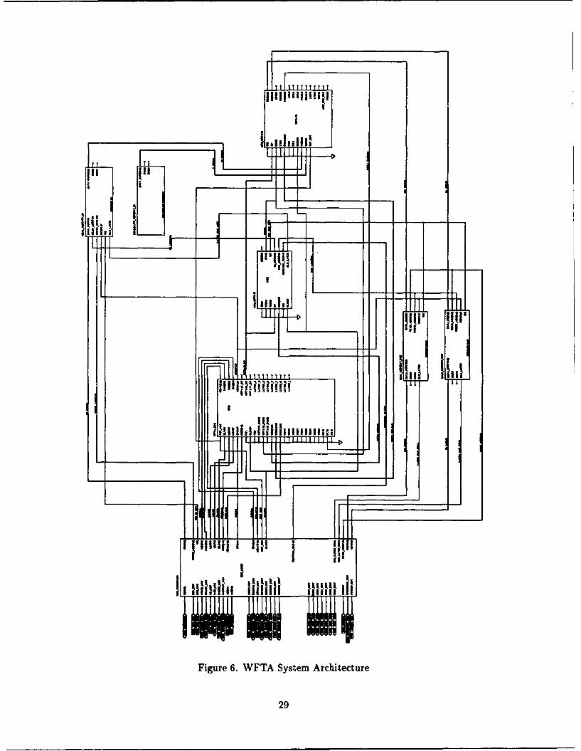
The modified architecture of the WFTA system of this thesis was briefly discussed in
Chapter III. This section covers the detailed design of the WFTA system. The architecture
described by Figure 2 was translated into the Synopsys SGE environment resulting in the
schematic shown in Figure 6. This figure includes all the signals and ports that were
required to be implemented in the final design of the single processor architecture.
28
II 111i ILI
114411
Figure 6. WFTA System Architecture
29
The first level functional decomposition discussed in Chapter III essentially forms the
structure for the rest of this chapter. Each first level component or major functional block
is discussed in the pages that follow. The complete set of schematics developed and used
for this thesis are located in Appendix K of this thesis. A few of these same schematics
are also included in this chapter and Appendix A to provide the reader with illustrations
of the written design. The major functional block timing diagrams showing the interrela-
tionships of signals are also provided in Appendix B. Additionally, the complete listing of
VHDL descriptions (both behavioral and structural) to include entity, architecture, and
configuration data is also located in Appendix K of this thesis.
Following a section on the behavioral description of the integrated circuits and other
modules used in the WFTA design, the specific and detailed descriptions of the structural
VHDL code of each of functional blocks are discussed.
4.3.1 Behavioral Descriptions. The intent of this VHDL development was to model,
as closely as possible, the actual design and construction of the proposed WFTA system.
The basic building blocks for this design are behavioral VHDL descriptions of integrated
circuits, modules which allow for future expansion, or modules used to model hardware
considerations. Starting with an high-level, abstract conception of the WFTA system, the
design can be functionally decomposed into hierarchically functional blocks using a top-
down design methodology. At the lowest level of the structural VHDL descriptions are the
behavioral VHDL descriptions discussed below.
4.3.1.1 Integrated Circuits. At the bottom of this hierarchically structural
WFTA system design are the actual chips used in the construction of the system. Taking
the specifications and datasheets of the integrated circuits [26, 27, 28], which describe the
function and timing of each of the chips used in the design, behavioral descriptions in
VHDL were written. Due to the great number of integrated circuits, a detailed discussion
of the behavioral VHDL descriptions is not possible, however, the behavioral VHDL can be
found in Appendix K. Table 1 provides a listing of the chips along with the filename of its
associated behavioral description. For the common chips, the behavioral descriptions used
are from the Synopsys library and are annotated SYNOPSYS in Table 1. In the MSPC, a
30
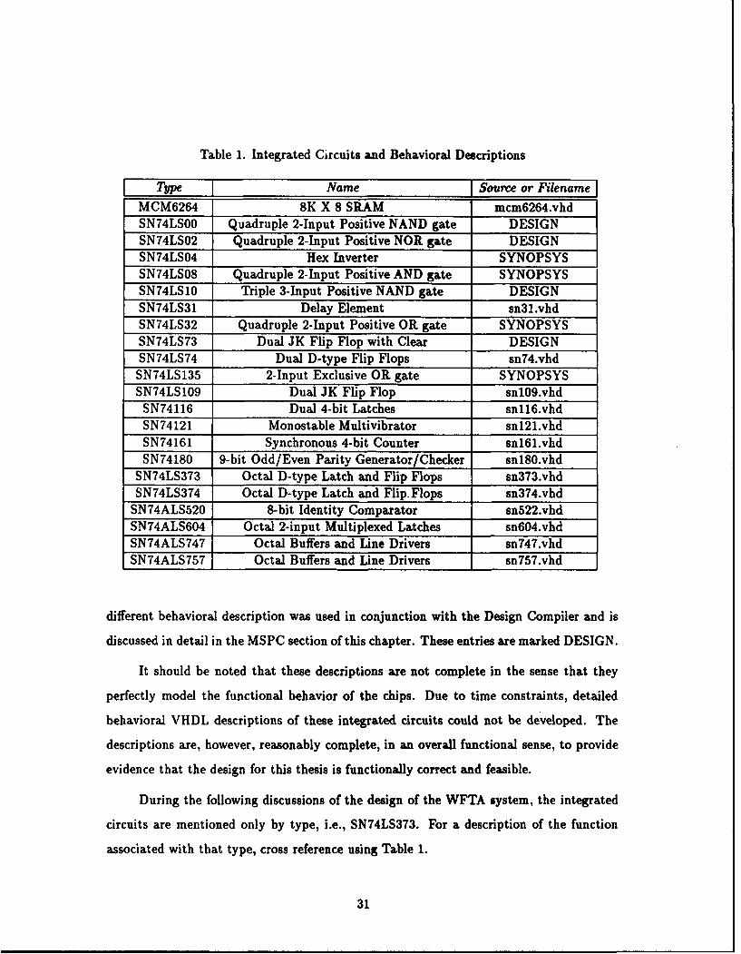
Table 1. Integrated Circuits and Behavioral Descriptions
Type Name Source or FilenameMCM6264 8K X 8 SRAM mcm6264.vhdSN74LSOO Quadruple 2-Input Positive NAND gate DESIGNSN74LS02 Quadruple 2-Input Positive NOR gate DESIGNSN74LS04 Hex Inverter SYNOPSYSSN74LS08 Quadruple 2-Input Positive AND gate SYNOPSYSSN74LS10 Triple 3-Input Positive NAND gate DESIGNSN74LS31 Delay Element sn3l.vhdSN74LS32 Quadruple 2-Input Positive OR gate SYNOPSYSSN74LS73 Dual JK Flip Flop with Clear DESIGNSN74LS74 Dual D-type Flip Flops sn74.vhdSN74LS135 2-Input Exclusive OR gate SYNOPSYSSN74LS109 Dual JK Flip Flop snl09.vhd
SN74116 Dual 4-bit Latches snll6.vhdSN74121 Monostable Multivibrator sn121.vhdSN74161 Synchronous 4-bit Counter snl6l.vhdSN74180 9-bit Odd/Even Parity Generator/Checker snl80.vhd
SN74LS373 Octal D-type Latch and Flip Flops sn373.vhdSN74LS374 Octal D-type Latch and Flip. Flops sn374.vhd
SN74ALS520 8-bit Identity Comparator sn522.vhdSN74ALS604 Octal 2-input Multiplexed Latches sn604.vhdSN74ALS747 Octal Buffers and Line Drivers sn747.vhdSN74ALS757 Octal Buffers and Line Drivers sn757.vhd
different behavioral description was used in conjunction with the Design Compiler and is
discussed in detail in the MSPC section of this chapter. These entries are marked DESIGN.
It should be noted that these descriptions are not complete in the sense that they
perfectly model the functional behavior of the chips. Due to time constraints, detailed
behavioral VHDL descriptions of these integrated circuits could not be developed. The
descriptions are, however, reasonably complete, in an overall functional sense, to provide
evidence that the design for this thesis is functionally correct and feasible.
During the following discussions of the design of the WFTA system, the integrated
circuits are mentioned only by type, i.e., SN74LS373. For a description of the function
associated with that type, cross reference using Table 1.
31
4.3.1.2 Modules for Future Enhancement or Hardware Consideration. There
were other modules of the design that were left in the behavioral VHDL format to either
simulate hardware considerations or provide room for future enhancements and modifica-
tions. A hardware consideration is a physical fact concerning construction, like grounding
or direct connections. These hardware considerations must be simulated in the VHDL
code. An example of a module simulating hardware considerations would be the a module
that grounds the imaginary input data lines to the APU. For those modules that are left for
future enhancements, the signals associated are discussed in [21 but were not implemented
in this initial system design. These files are enumerated below with a short explanation
for each concerning their functionality.
1. acu.not-used.vhd This file has been left for future enhancements of the VHDL code
and system design. This module includes signals which are not implemented in the
ACU design and makes no contribution to the VHDL simulation. This module was
included for completeness. Future researchers will be able to augment the system
design by coding functionality into the module.
2. grounded.vhd This file models a hardware consideration. These signals model the
physical property of wiring these signals to ground.
3. imag.in.vhd This file models a hardware consideration. As previously discussed, due
to lack of available memory chips, the imaginary input memory was not implemented.
In order to maintain logical continuity, this module models the grounded pins on the
WFTA processor.
4. interrupt, vhd This file has been left for future enhancements. For the maximum
throughput and speed the WFTA system needs to notify the host processor when
it has completed a FFT using an interrupt system instead of the host polling the
WFTA for completion.
5. memrncheck.vhd This file has been left for future enhancements. In the original design
of the WFTA, the memory was to have a memory error detection and correction
ability. This feature was not implemented with this thesis.
32
6. reset.vhd This file models a hardware consideration. Whenever the VMEbus resets,
this system reset would reset the WFTA board.
7. spc.not-used.vhd This file has been left for future enhancements. This module is
similar to the acu-noLtused.vhd file above. This module includes signals which are
not implemented in this MSPC design and was included for completeness.
4.S.1.3 Modules for Ease of Use in the Synopsys SGE Environment. The Syn-
opsys SGE environment does have certain operational limitations. These files provided a
bypass for the schematic graphical environment's safeguards. One of the problems encoun-
tered in this thesis was the inability to connect two named nets directly in the schematic.
A named net is a specific node of a circuit and the SGE tool does not allow a node to
have more than one name. The two files straight.vhd & straightl.vhd were used make this
connection possible. The VHDL code simply assigns the incoming signal to the outgoing
signal. Another problem is that GND and VCC are not associated with the MVL7 values
'0' and '1', respectively. This problem was dealt with using a package called wfta-types.vhd
which makes a default assignment with GND assigned '0' and VCC assigned '1'. Also
included in this file are a few type conversion functions which are necessary for the use of
previously created VHDL behavioral code for the WFTA processor or APU. Each struc-
tural description generated from the schematic includes this file in order to eliminate this
problem.
4.3.2 Common Gates. Throughout the design, there are several instantiations of
standard logic gates, such as AND gates, inverter gates, and the like. The behavioral
descriptions used for these gates are the ones found in the Synopsys standard library. The
propagation delays for these gates defaults to 0 nanoseconds for both THL (propagation
delay from input high to output low) and TLH (propagation delay from input low to output
high). This instantaneous result is not indicative of actual timing delays, and in order to
simulate the constructed system, reasonable values for timing were mapped to the generic
map of these behavioral descriptions. In the VHDL code developed for this thesis the times
annotated in Table 2 are used in all the VHDL simulations. The times that are used in
33
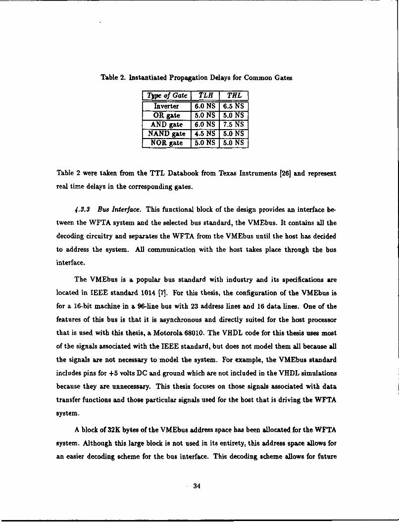
Table 2. Instantiated Propagation Delays for Common Gates
Tnpe of Gate TLH THL
Inverter 6.0 NS 6.5 NSOR gate 5.0 NS 5.0 NS
AND gate 6.0 NS 7.5 NSNAND gate 4.5 NS 5.0 NSNOR gate 5.0 NS 5.0 NS
Table 2 were taken from the TTL Databook from Texas Instruments [26] and represent
real time delays in the corresponding gates.
4.3.3 Bus Interface. This functional block of the design provides an interface be-
tween the WFTA system and the selected bus standard, the VMEbus. It contains all the
decoding circuitry and separates the WFTA from the VMEbus until the host has decided
to address the system. All communication with the host takes place through the bus
interface.
The VMEbus is a popular bus standard with industry and its specifications are
located in IEEE standard 1014 [7]. For this thesis, the configuration of the VMEbus is
for a 16-bit machine in a 96-line bus with 23 address lines and 16 data lines. One of the
features of this bus is that it is asynchronous and directly suited for the host processor
that is used with this thesis, a Motorola 68010. The VHDL code for this thesis uses most
of the signals associated with the IEEE standard, but does not model them all because all
the signals are not necessary to model the system. For example, the VMEbus standard
includes pins for +5 volts DC and ground which are not included in the VHDL simulations
because they are unnecessary. This thesis focuses on those signals associated with data
transfer functions and those particular signals used for the host that is driving the WFTA
system.
A block of 32K bytes of the VMEbus address space has been allocated for the WFTA
system. Although this large block is not used in its entirety, this address space allows for
an easier decoding scheme for the bus interface. This decoding scheme allows for future
34
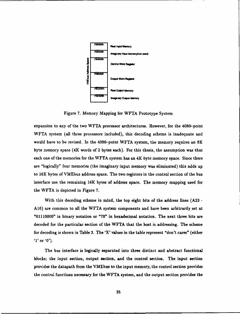
7•OO ;x( eAs Inp* -~r700000h Re pt ft m70 in2ay Wpid Me-mry(not u-M
70O40 0 0h C n a O o w
, •Oui Word Rapdi
Real OuIp Memcy
hna~wy OuW Memcey
Figure 7. Memory Mapping for WFTA Prototype System
expansion to any of the two WFTA processor architectures. However, for the 4080-point
WFTA system (all three processors included), this decoding scheme is inadequate and
would have to be revised. In the 4080-point WFTA system, the memory requires an 8K
byte memory space (4K words of 2 bytes each). For this thesis, the assumption was that
each one of the memories for the WFTA system has an 4K byte memory space. Since there
are "logically" four memories (the imaginary input memory was eliminated) this adds up
to 16K bytes of VMEbus address space. The two registers in the control section of the bus
interface use the remaining 16K bytes of address space. The memory mapping used for
the WFTA is depicted in Figure 7.
With this decoding scheme in mind, the top eight bits of the address lines (A23 -
A16) are common to all the WFTA system components and have been arbitrarily set at
"01110000" in binary notation or "70" in hexadecimal notation. The next three bits are
decoded for the particular section of the WFTA that the host is addressing. The scheme
for decoding is shown in Table 3. The 'X' values in the table represent "don't cares" (either
'1' or '0').
The bus interface is logically separated into three distinct and abstract functional
blocks; the input section, output section, and the control section. The input section
provides the datapath from the VMEbus to the input memory, the control section provides
the control functions necessary for the WFTA system, and the output section provides the
35
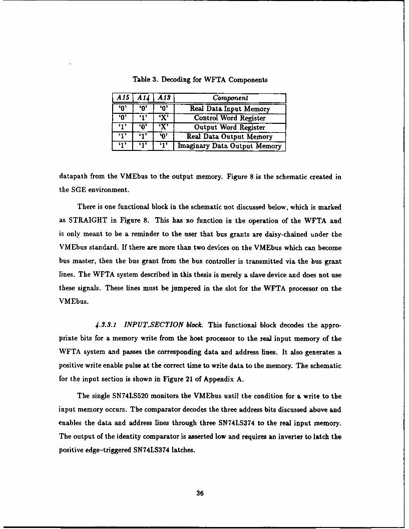
Table 3. Decoding for WFTA Components
I A151 A141 A131 Component'0' '0' '0' Real Data Input Memory'0' '1' 'X' Control Word Register'1' '0' 'X' Output Word Register'1' '1' '0' Real Data Output Memory'1' '1' '1' Imaginary Data Output Memory
datapath from the VMEbus to the output memory. Figure 8 is the schematic created in
the SGE environment.
There is one functional block in the schematic not discussed below, which is marked
as STRAIGHT in Figure 8. This has no function in the operation of the WFTA and
is only meant to be a reminder to the user that bus grants are daisy-chained under the
VMEbus standard. If there are more than two devices on the VMEbus which can become
bus master, then the bus grant from the bus controller is transmitted via the bus grant
lines. The WFTA system described in this thesis is merely a slave device and does not use
these signals. These lines must be jumpered in the slot for the WFTA processor on the
VMEbus.
4.3.3.1 INPUT-SECTION block. This functional block decodes the appro-
priate bits for a memory write from the host processor to the real input memory of the
WFTA system and passes the corresponding data and address lines. It also generates a
positive write enable pulse at the correct time to write data to the memory. The schematic
for the input section is shown in Figure 21 of Appendix A.
The single SN74LS520 monitors the VMEbus until the condition for a write to the
input memory occurs. The comparator decodes the three address bits discussed above and
enables the data and address lines through three SN74LS374 to the real input memory.
The output of the identity comparator is asserted low and requires an inverter to latch the
positive edge-triggered SN74LS374 latches.
36
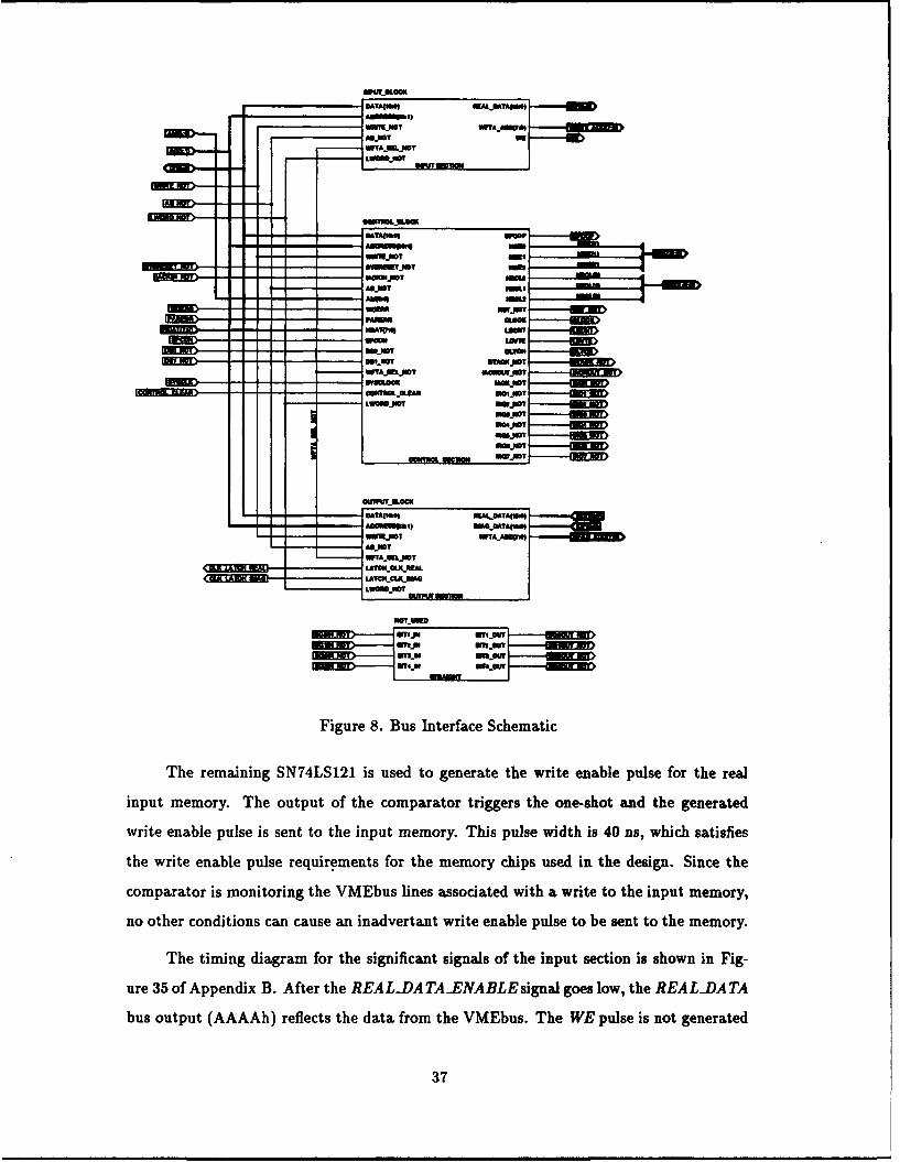
- TAO"i) IMALMA(UP-T
VO IYI.PWT •irAD- .AS.OT WE
•,---
------E.,-
LIiIENKF-mm igure,8..Bus nerac Shmati
inu eoy h otu ftecmprtrtigr them one-sho-an-tegnerte
eMUrMT el
Figur win -u Inter--ce Seaic
write enable pulse is sent to the input memory. This pulse width is 40 ns, which satisfies
the write enable pulse requirements for the memory chips used in the design. Since the
comparator is monitoring the VMEbus lines associated with a. write to the input memory,
no other conditions can cause an inadvertant write enable pulse to be sent to the memory.
The timing diagram for the significant signals of the input section is shown in Fig-
ure 35 of Appendix B. After the REALDATA..ENABLEsignal goes low, the REALJATA
bus output (AAAAh) reflects the data from the VMEbus. The WE pulse is not generated
37
until after the ouput data from the input section is valid. The only signal here which needs
further explanation is the WFTA.ADD address. The address on the VMEbus is shown as
700004h and the address that is output from the input section is 02h. This seeming dis-
crepancy is caused by the VMEbus addressing scheme. The VMEbus is byte-addressable
while the WFTA is word-addressable. Address 4 on the VMEbus corresponds to the first
byte of the second word (or address 2) in the WFTA memory. So, the WFTA is operating
correctly. This addressing difference will be also be evident in the output section.
It should be noted that since the comparator monitors the WRITE-NOT signal on
the VMEbus, a read from the input memory is not possible. Additionally, given the design
of the input memory, a read is not possible because no datapath exists back to the VMEbus
from the input memory. Data can only move forward through the WFTA system.
4.3.3.2 CONTROL-SECTION block. This functional block provides the means
for the host processor to control the WFTA system. The heart of this section are two regis-
ters called the control register and the output register. Through these two 16-bit registers
the host processor starts the WFTA and determines when the WFTA is finished calculating
the FFT. The schematic for the control section is shown in Figure 22 of Appendix A.
In order to decrease the decoding circuitry for the prototype WFTA system, three
SN74LS520 decode those signals common to all WFTA system accesses. These signals
are comprised of the top eight bits of the address lines, the address modifier lines, the
DSONOT and DS1_NOT data strobe lines, and the LWORD.NOT lines. Since these
signals are the same for all WFTA system accesses, they can be monitored centrally here
in this section and the other sections (input and output sections) can be informed when the
signals occur. Table 4 shows the VMEbus signals that are constant and do not change over
all WFTA accesses. When the WFTA system is addressed, these comparators generate
a signal (WFTA-SEL.NOT) through a series of OR gates which are sent to the other
two sections of the bus interface. All three sections use the WFTASEL-NOT signal in
conjunction with other signals specific to their operation to determine whether they are
being addressed by the host.
38
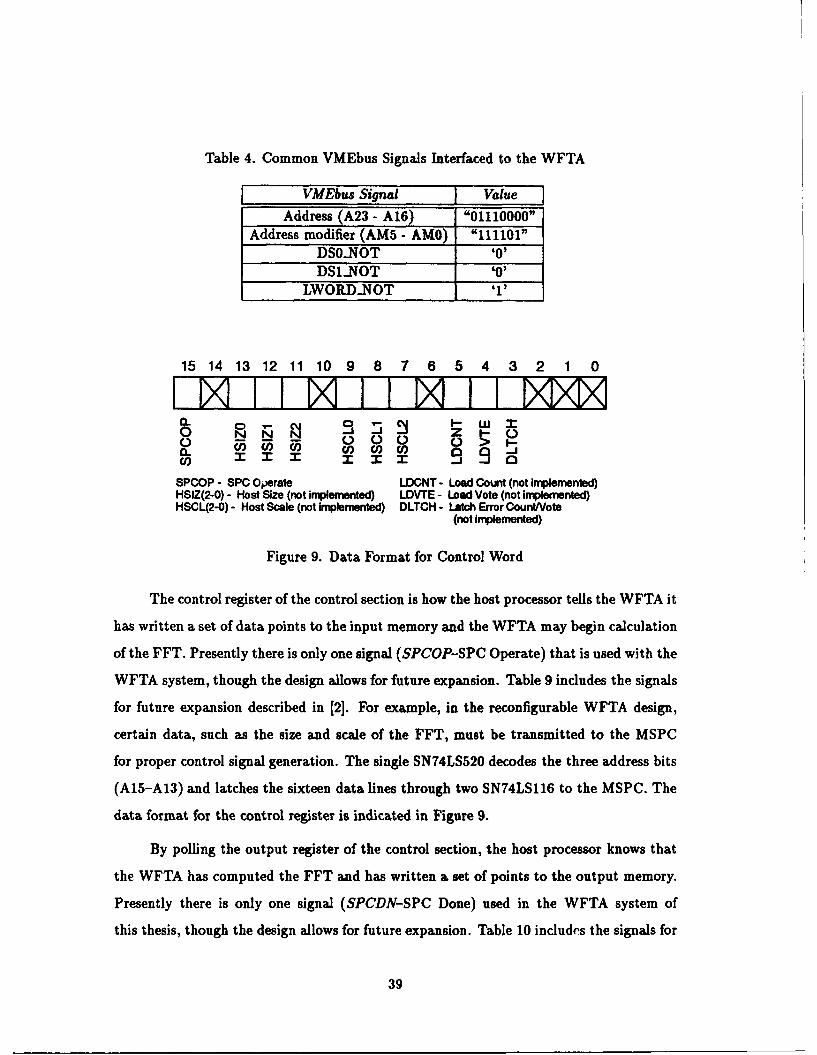
Table 4. Common VMEbus Signals Interfaced to the WFTA
VMEbus Signal ValueD
Address (A23 - A16) "01110000"Address modifier (AM5 - AMO) "111101"
DS0NOT 4'0'
DSINOT '0'LWORDNOT 4'1'
15 14 13 12 11 10 9 8 7 6 5 4 3 2 1 0
INI 'MN i 1 I II IIT xo NN"a. .,- R1 I--W.
-j-
SPCOP - SPC Operate LDCNT- Load Count (not Iiplemented)HSIZ(2-0) - Host Size (not implemented) LDVTE - Load Vote (not implemented)HSCL(2-0) - Host Scale (not Implemented) DLTCH - Latch Error CountVote
(not implemented)
Figure 9. Data Format for Control Word
The control register of the control section is how the host processor tells the WFTA it
has written a set of data points to the input memory and the WFTA may begin calculation
of the FFT. Presently there is only one signal (SPCOP-SPC Operate) that is used with the
WFTA system, though the design allows for future expansion. Table 9 includes the signals
for future expansion described in [2]. For example, in the reconfigurable WFTA design,
certain data, such as the size and scale of the FFT, must be transmitted to the MSPC
for proper control signal generation. The single SN74LS520 decodes the three address bits
(A15-A13) and latches the sixteen data lines through two SN74LS116 to the MSPC. The
data format for the control register is indicated in Figure 9.
By polling the output register of the control section, the host processor knows that
the WFTA has computed the FFT and has written a set of points to the output memory.
Presently there is only one signal (SPCDN-SPC Done) used in the WFTA system of
this thesis, though the design allows for future expansion. Table 10 includes the signals for
39
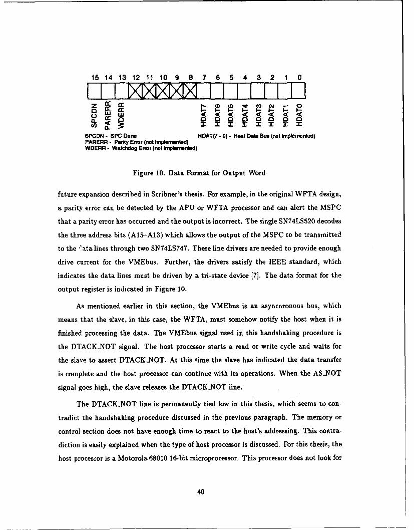
15 14 13 12 11 10 9 8 7 6 5 4 3 2 1 0
U) <~
SPCDN - SPC Done HDAT(7 -0) - Host Data Bus (not Implemented)PARERR - Parity Error (not Implemented)WDERR - Watchdog Error (not ipWlemented)
Figure 10. Data Format for Output Word
future expansion described in Scribner's thesis. For example, in the original WFTA design,
a parity error can be detected by the APU or WFTA processor and can alert the MSPC
that a parity error has occurred and the output is incorrect. The single SN74LS520 decodes
the three address bits (A15-A13) which allows the output of the MSPC to be transmitted
to the ' ata lines through two SN74LS747. These line drivers are needed to provide enough
drive current for the VMEbus. Further, the drivers satisfy the IEEE standard, which
indicates the data lines must be driven by a tri-state device [7]. The data format for the
output register is indicated in Figure 10.
As mentioned earlier in this section, the VMEbus is an asyncnironous bus, which
means that the slave, in this case, the WFTA, must somehow notify the host when it is
finished processing the data. The VMEbus signal used in this handshaking procedure is
the DTACKNOT signal. The host processor starts a read or write cycle and waits for
the slave to assert DTACK.NOT. At this time the slave has indicated the data transfer
is complete and the host processor can continue with its operations. When the AS-NOT
signal goes high, the slave releases the DTACKNOT line.
The DTACKNOT line is permanently tied low in this thesis, which seems to con-
tradict the handshaking procedure discussed in the previous paragraph. The memory or
control section does not have enough time to react to the host's addressing. This contra-
diction is easily explained when the type of host processor is discussed. For this thesis, the
host processor is a Motorola 68010 16-bit microprocessor. This processor does not look for
40
the DTACKNOT signal assertion until the falling edge of its own state 4, which is 250
ns after the cycle has begun [29]. This 250 ns time is enough for either a read or write to
memory or a read or write to the control and output registers. Simply stated, the WFTA
system is able to finish the cycle before the 68010 can reply. With a faster processor this
convenience might not be possible.
The DTACKNOT signal, tied low, goes through a SN74LS757 which is enabled
when any part of the WFTA is selected. This line driver is necessary to provide adequate
current to the VMEbus line. Furthermore, the DTACKNOT line must be an open collector
output [7].
The RESET block simply routes the VMEbus SYSRESET line to the WFTA. When
the VMEbus resets, the WFTA system is forced to a known start state. This reset signal
(RSTNOT) propagates through the design to drive flip flops and the finite state machine
of the MSPC to a known state. Initially when the system is first powered up, the bus
master propagates this signal to the entire bus.
The VMEbus SYS-CLOCK signal operates at 16 MHz. The clock block of the
control section is simply a frequency divider which takes the 16 MHz and generates an
8 MHz system clock for the WFTA. This frequency divider is a SN74LS109 in a toggle
configuration. The 8 MHz gives the WFTA a 100 nanosecond period with approximately
a 75 % duty cycle. The signal is asymmetrical because of the propagation timing of the
SN74LS109. The propagation time for a low to high transition of the output is 13 ns and for
"a high to low transition of the output is 25 ns. The WFTA system operates correctly using
"a clock with a 75 % duty cycle. This clock has been left as a block for future expansion
when the WFTA will be required to operate at faster speeds and a different clock will have
to be used.
The timing diagram for the significant signals of the control section are shown in
Figure 36 and Figure 37 of Appendix B. The timing diagram is broken into two parts;
Figure 36 shows a write to the control word and Figure 37 shows a read from the output
word. In Figure 36, the VMEbus address lines are 704000h which maps to the control word
access and the VMEbus data lines read 8000h which corresponds to the host telling the
41
MSPC to begin operation. The control section responds by driving the SPCOP signal high
after approxiamately 20 ns. In Figure 37, the VMEbus address lines are 708000h which
maps to a ouput word access. The control section responds by driving the VMEbus data
lines to an arbitrary 8055h. If the host were polling this would indicate that the MSPC
has completed the FFT calculation. Notice in both figures that the VMEbus dock has
been divided and the WFTA system clock is operating at twice the period.
The interrupt handler has already been mentioned in the behavioral section and
has not been implemented in this thesis cycle. It is only here to provide room for future
expansion.
4.3.3.3 OUTPUT-SECTION Block. This functional block decodes the ap-
propriate bits for a memory read from the host processor to the real and imaginary output
memory of the WFTA system and passes the appropriate address lines. It also generates a
latch signal which tells the memory when to output data to the output section and through
bus drivers to the data lines on the VMEbus. The schematic for the output section is shown
in Figure 23 of Appendix A.
There are two SN74LS520's to decode whether the host is addressing the real output
memory or the imaginary output memory. The two outputs of the identity comparators
are tied to an AND gate which enables and clocks a SN74LS374 transmitting the desired
address to the output memory.
Due to the design of the memory, the output section must also transmit a control
signal to the output memory indicating when the multiplexers are to latch data from
the memory chips. The two SN74LS31 are used to delay the outputs of the identity
comparators long enough for the memory to be accessed. These two control signals are
the LATCHCLK.REAL and the LATCHCLK.IMAG signals. The outputs of the identity
comparators are asserted low and requires two inverters to latch the positive edge-triggered
SN74LS374 latches.
The two sets of two SN74LS747's drive the VMEbus data lines with the output of
the real and imaginary output memories. Again, as mentioned previously, the data lines
must be driven by a tri-state device.
42
The timing diagram for the significant signals of the output section are shown in
Figure 38 and Figure 39 of Appendix B. The timing diagram is broken into two parts;
Figure 38 shows a read from the real output memory and Figure 39 shows a read from the
imaginary output memory. In Figure 38, the VMEbus address lines are 70C004h which
maps to a real output memory access. The difference in the VMEbus address lines and the
WFTAADD lines was discussed in the input section previously. In Figure 39, the VMEbus
address lines are 70EO004h which maps to an imaginary output memory access. In both
figures, the output section responds by sending a latch signal (either LATCHCLKJREAL
or LATCHICLKJIMAG) to the output memory and then driving the VMEbus data lines
with the memory output.
It should be noted that since the comparator monitors the WRITE-NOT signal
on the VMEbus for logic high, the host cannot execute a write to the output memory.
Additionally, given the design of the output memory, a write is not possible since a datapath
to the output memory from the host does not exist. Data can only flow from the APU to
the output memory.
4.3.4 Input and Output Memory. The memory functional blocks include both the
input memory and the output memory. Data is written by the host into the input memory
and, conversely, data is read by the host from the output memory. The problem with the
memory was to construct a dual bank of memory that is switchable, that is, with one bank
accessible by the host processor over the VMEbus and the other bank holding data for the
APU with both banks accessible at the same time. While the APU is operating with a set
of data, the host is loading a new set of points into the next bank. This bank switchable
feature increases the overall throughput of the system.
The original WFTA design called for an application-specific memory chip which
would perform this dual access with one bank of memory always accessible from either the
host or the APU. However, this component was not available at the time of this thesis and
had to be constructed discretely with commercially available chips.
In this design, 12K of VMEbus address space has been allocated to the memory
in consideration of the 4080-point processor that was envisioned by earlier designers. In
43
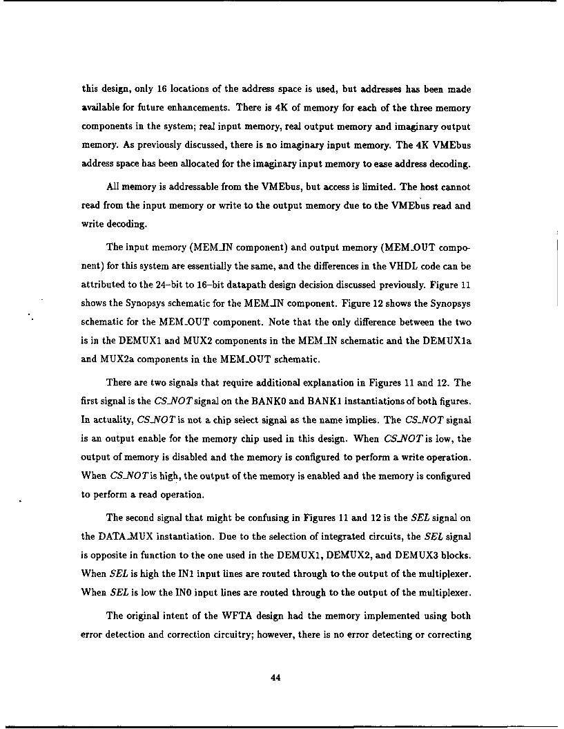
this design, only 16 locations of the address space is used, but addresses has been made
available for future enhancements. There is 4K of memory for each of the three memory
components in the system; real input memory, real output memory and imaginary output
memory. As previously discussed, there is no imaginary input memory. The 4K VMEbus
address space has been allocated for the imaginary input memory to ease address decoding.
All memory is addressable from the VMEbus, but access is limited. The host cannot
read from the input memory or write to the output memory due to the VMEbus read and
write decoding.
The input memory (MEMIN component) and output memory (MEMOUT compo-
nent) for this system are essentially the same, and the differences in the VHDL code can be
attributed to the 24-bit to 16-bit datapath design decision discussed previously. Figure 11
shows the Synopsys schematic for the MEMIN component. Figure 12 shows the Synopsys
schematic for the MEMOUT component. Note that the only difference between the two
is in the DEMUX1 and MUX2 components in the MEMIN schematic and the DEMUXla
and MUX2a components in the MEMOUT schematic.
There are two signals that require additional explanation in Figures 11 and 12. The
first signal is the CSJNOT signal on the BANKO and BANK 1 instantiations of both figures.
In actuality, CS.NOT is not a chip select signal as the name implies. The CS-NOT signal
is an output enable for the memory chip used in this design. When CS.NOT is low, the
output of memory is disabled and the memory is configured to perform a write operation.
When CS..NO T is high, the output of the memory is enabled and the memory is configured
to perform a read operation.
The second signal that might be confusing in Figures 11 and 12 is the SEL signal on
the DATA.MUX instantiation. Due to the selection of integrated circuits, the SEL signal
is opposite in function to the one used in the DEMUX1, DEMUX2, and DEMUX3 blocks.
When SEL is high the IN1 input lines are routed through to the output of the multiplexer.
When SEL is low the INO input lines are routed through to the output of the multiplexer.
The original intent of the WFTA design had the memory implemented using both
error detection and correction circuitry; however, there is no error detecting or correcting
44
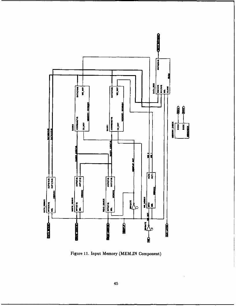
ii
II
II ItIi DI
Figure 11. Input Memory (MEMJIN Component)
45
II IIIac
I i ii-IL 1I
Figure 12. Output Memory (MEMOUT Component)
46
logic in this design. This circuitry is missing due to space and chip count restrictions on
the size of the finished prototype.
The memory is functionally decomposed into five subsections, to be discussed in
detail in the sections that follow. The demultiplexer blocks route the address, data, and
write enable signals to the appropriate bank of memory, while the multiplexer block routes
the data from one of the banks to the APU. The schematics for these functional blocks
are shown in Appendix A. After all of the functional blocks are discussed and the major
signals introduced, there is a short discussion of the timing diagrams of both the input and
output memory. The timing diagrams for the memories are shown in Figures 40 and 41 of
Appendix B.
4.3.4.1 DEMUX1 & DEMUXia Block. This block routes the incoming data
lines to the appropriate bank of memory. Depending on the control signal generated by the
MSPC, the incoming data is routed and written to the only one bank of memory. The other
bank of memory is oriented towards the ACU and APU. The schematics for the DEMUX1
and DEMUXla blocks are shown in Figures 24 and 25, respectively, of Appendix A.
This is one of the blocks which is different between the input memory and the output
memory. The DEMUXI block is used in the input memory while the DEMUXla block is
used in the output memory. Both use four SN74ALS373's. This block allows data to pass
to all four SN74ALS373's but enables the output of only two of them based on the select
signal generated by the MSPC. Only two of these latches are enabled at one time due to
the inverter gate which separates the two enable pins. Two latches are necessary for the
16 bits of data-one for the upper eight bits of data and the other for the lower eight bits
of data.
The only difference between the two blocks is the number of data bits that are input
into the memory. In the case of DEMUXla block, there are 8 bits of data from the APU
which are never used as the APU still sends 24 bits of output data instead of the 16
bits which the system was designed to accept. Bit 7 through bit 0, which are the least
significant in this data format, are the bits which are discarded. Functionally, there are no
other differences between the two components.
47
4.3.-4.2 DEMUX2 Block. This block routes the incoming address lines of the
memory to the appropriate bank of memory. There are two of these blocks in the input
memory and output memory schematics because the memory has the ability to read and
write from the separate banks at one time. The structural configuration of the memory and
the select line from the MSPC make this simultaneous transfer possible. Again, depending
on the control signal generated by the MSPC, the incoming address lines are routed to the
appropriate bank of memory. The schematic for the DEMUX2 block is shown in Figure 26
of Appendix A.
This block is similar to the previous section in its implementation. Instead of four
SN74ALS373, there are only two latches because the number of bits of data in this case is
eight instead of sixteen. Again only one of the latches is enabled at one time due to the
inverter gate which separates the two enable pins. Although, technically, the memory for
this system needs only four bits of address for the 16 words that are written to memory,
eight bits were passed for future enhancement.
4.3.-4.3 DEMUX3 Block. This block routes the incoming positive logic write
enable pulse to the appropriate bank of memory. Depending on the control signal generated
by the MSPC, this block routes the write enable pulse to correct bank of memory. The
schematic for the DEMUX3 block is shown in Figure 27 of Appendix A.
There is a subtle diffeienre in this block versus the other DEMUX blocks discussed
above because instead of a high impedance output on the non-selected signal there must
be a high output. This is necessary to prevent unwanted writes to the non-selected bank
of memory. Since the write enable for the memory is negative logic, this block also serves
to translate the positive write enable pulse from the ACU into a negative pulse that can be
used by the memory. For this reason a SN74LS74 was used. It is used asynchronously with
the control signal either enabling the clear or preset function of the flip flop. An inverter
between the two pins prevents enabling both the clear and the preset pins at the same
time. However, there exists a finite time (propagation delay of the inverter) when the clear
and preset are momentarily the same. This is not a problem because it does not generate
a write enable pulse. According to the specifications for the SN74LS74 [261, when both
48
dear and preset are high the output is the stored value and when both dear and preset
are low the output is high on Q and QNOT. The write enable pulse from the ACU or the
VMEbus interface is not generated for approxiamately 100 ns, which allows enough time
for the signals in this block to transition to their proper values.
The two outputs of the flip flop (Q and QNOT) are input to two OR gates and,
depending on which output is zero, the active low write enable pulse from the ACU or
VMEbus interface is directed to the correct bank of memory. Since Q and QNOT are not
the same, only one of the OR gates will allow the write enable pulse to pass through to
the memory chips.
4.3.4.4 MEM-MCM6264 Block. This block is essentially a bank of memory
using two Motorola MCM6264 chips to store a single 16-bit word. One of the chips stores
the upper eight bits of data while the other stores the lower eight bits of data. Although
only the lower seven addresses are used for this chip, only 16 words are stored at one time
for this single configuration architecture leaving a large amount of memory left for future
enhancements. The schematic for the MEM-MCM6264 block is shown in Figure 28 of
Appendix A.
This additional memory bandwidth was necessary because of the lack of commercially
available chips that would have been more suitable for the WFTA. There is apparently
no commercial demand for a 16 word 16-bit memory. The design decision was to use a
larger capacity chip which could store a longer word of memory and be relatively fast.
After careful consideration of the available choices, the Motorola MCM6264 8K X 8 Static
random access memory (SRAM) chip was chosen as it satisfied these requirements. After
searching available memory chips, the "ideal" memory chips for this thesis are scarce in
the industry.
Static RAM was selected over dynamic RAM for a number of reasons. The increased
speed of memory access for both reads and writes, although for this particular host pro-
cessor are not critical, is desirable for increased speed of the overall device. Some dynamic
RAM memories also require additional chips for control and refresh circuitry which would
have added additional chips to the total chip count which was undesirable. Further, dy-
49
namic RAM is more dense with generally more words of storage of shorter word length.
The memory required must be able to store 16-bit words from the host and using dynamic
RAM would have wasted memory versus less waste for any static RAM configurations.
4.3.-4.5 MUX2 & MUX2a Block. This block is the interface between the out-
put of the memory banks and the output of the memory component. Based on the control
signal from the MSPC discussed below, the correct input is selected between the two mem-
ory banks outputs and multiplexed out of the memory. The schematics for the MUX2 and
MUX2a blocks are shown in Figures 29 and 30, respectively, of Appendix A.
These blocks are structurally different between the input memory and the output
memory. The MUX2 block is used in the input memory while the MUX2a block is used in
the output memory. Both blocks use two SN74ALS604, one for the upper eight bits and
the other for the lower eight bits. The difference between the two blocks is in the addition
of two SN747180 in the MUX2 block which are used to generate the odd parity bit (bit 0)
needed for the APU. One calculates the odd parity of the upper eight bits, and the other
calculates parity for the lower eight bits. These two outputs are fed into an exclusive-OR
which then calculates the entire parity of the 16 bit word. The remaining seven bits of
the output of the memory input have been grounded, to account for the difference in the
24-bit versus 16-bit data words.
4.3.-4.6 Input and Output Memory Timing Diagrams. The timing diagram
for the input memory is shown in Figure 40 of Appendix B and the timing diagram for
the output memory is shown in Figure 41 of Appendix B. The two timing diagrams are
similar because, functionally, both of the memories operate exactly the same and the two
test benches used to generate these timing diagrams used similar input test vectors. The
only differences have already been discussed in Sections 4.3.4.1 and 4.3.4.5. The input
memory reads in 16 bits of data and outputs 24 bits of data with a generated parity bit,
while the output memory reads in 24 bits of data and outputs 16 bits of data. The other
signals are the same, only the sources of the signals are different.
50
In both timing diagrams, the input data (DATA.IN) changes halfway through the
simulation. Also notice that the MEM..FLIP signal changes at the same time that the data
changes. The two addresses to both memories (BANKI.ADD and BANKO.ADD) remain
the same for these simulations. MEMFLIP is the most important signal in the memory
because it controls the flow of data to and from the correct bank of memory. All the inputs
of the two banks of memory are also shown in both timing diagrams.
In Figure 40, the input memory initially receives 16 bits of data (5555h) from the
VMEbus interface. MEM..FLIPis high which routes the data to memory bank 1 (DATA1).
The WE pulse from the VMEbus interface gets routed to memory bank 1 (WE-1). This
causes the input data to be written to address 3 (BANKIADD) of memory bank 1.
Meanwhile, memory bank 0 is reading from address 8 (BANK.ADD) and after the odd
parity bit is calculated outputs this to the APU (DATA-OUT). During the second half of
the simulation, the MEM.FLIP signal is low, wldch causes the input data (AAAAh) to be
written to bank 0 (DATAO) and the output data to be read from bank 1 (DATAOUT).
Except for the differences in size of the input and output data, and the generation of the
parity bit, Figure 41 describes the same operations described above.
4.3.5 ACU. The Arithmetic Control Unit (ACU) was one of the functional blocks
which is ultimately destined to be an application-specific integrated circuit for incorpora-
tion into the WFTA system. However, since this module is presently not available for this
thesis, it has been designed using discrete components. Many of the functions of the ACU
described in earlier theses, such as the watchdog functions, are not implemented in this
discrete design for simplification reasons.
The ACU works hand-in-hand with the APU and provides the necessary address
lines to both the input and output memory, as well as the write enable pulse to the output
memory. Timing is critical between the ACU and the APU and is based solely on a count
of clock cycles. The ACU also provides a done signal to inform the MSPC that the FFT
has been calculated and loaded into the output memory.
For this single processor architecture, the memory access is sequential or data points
are read one after the other into the APU. This is true for the 15, 16, and 17-point trans-
51
form sizes, however, this is not true of the ACU that is used in the reconfigurable WFTA
architecture which calculates larger transform sizes. The Prime Factor Algorithm (PFA)
demands that the addressing of data be in a non-sequential but determinable pattern. This
ACU only works in the single processor architecture described by Figure 6.
The ACU is functionally decomposed into four subsections discussed in detail in the
sections that follow. The initialize block waits the appropriate number of clock cycles nec-
essary before the APU is prepared to accept data. The counter block counts the necessary
number of clock cycles before enabling addresses to the output memory. The two address
blocks output the addresses and write enable to either the input or output memory at the
correct time. Figure 13 shows the schematic indicating the relationship of these functional
blocks.
Presently, the ACU has been designed to be used with only one of the WFTA pro-
cessors, the 16-point processor. The different latency times of the other FFT processors
and different number of addresses used by each make a configurable discrete ACU more
complicated to design. In order to keep chip count of the design a minimum, this ACU
was only designed to work with a single processor.
Since the APU takes inputs and outputs on the falling edge of every second clock
pulse, the SN74109 pictured in the schematic divides the clock signal. This chip was needed
to provide the two sub-components, ACUADD and ACUADD1, with a signal required
to change their respective memrory addresses.
The CONTROL-CLEAR control signal is sent back to the bus interface to clear the
control register which controlls the MSPC. This signal is necessary because if the signal is
not present the MSPC, in its current design, would continue to calculate FFT's without
termination.
After discussing the four subsections composing the ACU, the timing diagrams for
the ACU are discussed in Figures 42 and 43 of Appendix B. These timing diagrams can
be referenced during the discussions of the four subsections for specific relationships.
4.3.5.1 ACU-INIT Block. This functional block delays the ACU six clock
cycles before enabling the addresses to the input memory. The APU needs this six clock
52
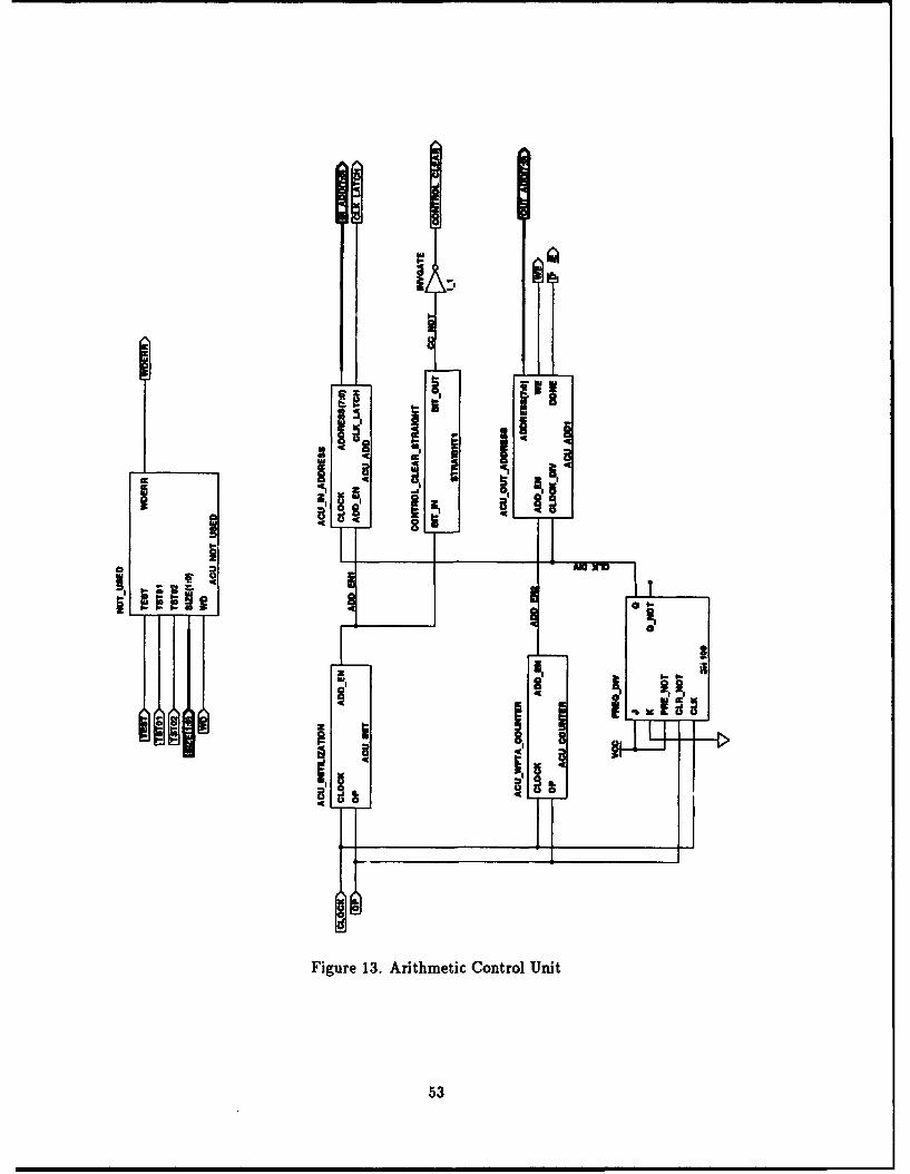
O-
,0 1i
Figure 13. Arithmetic Control Unit
53
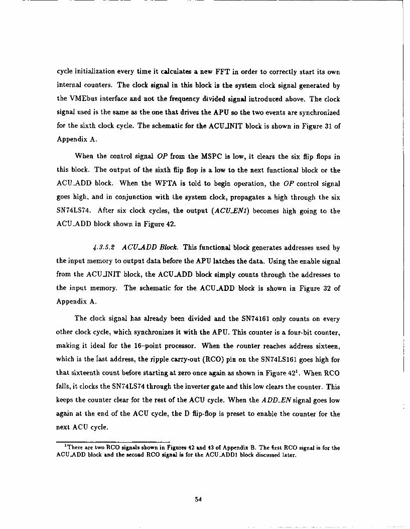
cycle initialization every time it calculates a new FFT in order to correctly start its own
internal counters. The clock signal in this block is the system clock signal generated by
the VMEbus interface and not the frequency divided signal introduced above. The clock
signal used is the same as the one that drives the APU so the two events are synchronized
for the sixth clock cycle. The schematic for the ACU.INIT block is shown in Figure 31 of
Appendix A.
When the control signal OP from the MSPC is low, it clears the six flip flops in
this block. The output of the sixth flip flop is a low to the next functional block or the
ACUADD block. When the WFTA is told to begin operation, the OP control signal
goes high, and in conjunction with the system clock, propagates a high through the six
SN74LS74. After six clock cycles, the output (ACUEN1) becomes high going to the
ACUADD block shown in Figure 42.
4.3.5.2 ACUADD Block. This functional block generates addresses used by
the input memory to output data before the APU latches the data. Using the enable signal
from the ACUINIT block, the ACUADD block simply counts through the addresses to
the input memory. The schematic for the ACU.ADD block is shown in Figure 32 of
Appendix A.
The clock signal has already been divided and the SN74161 only counts on every
other clock cycle, which synchronizes it with the APU. This counter is a four-bit counter,
making it ideal for the 16-point processor. When the counter reaches address sixteen,
which is the last address, the ripple carry-out (RCO) pin on the SN74LS161 goes high for
that sixteenth count before starting at zero once again as shown in Figure 421. When RCO
falls, it clocks the SN74LS74 through the inverter gate and this low clears the counter. This
keeps the counter clear for the rest of the ACU cycle. When the ADDEN signal goes low
again at the end of the ACU cycle, the D flip-flop is preset to enable the counter for the
next ACU cycle.
'There are two RCO signals shown in Figures 42 and 43 of Appendix B. The first RCO signal is for theACU.ADD block and the second RCO signal is for the ACU.ADDI block discussed later.
54
Due to the design of the memory, the ACU.ADD block must also transmit a control
signal to the input memory indicating when the multiplexers are to latch data from the
memory chips. The ADDEN signal and CLOCK signal are input to an AND gate to
determine when the counter generating the addresses increments the address count. The
SN74LS31 is used to delay this signal long enough (100 ns) for the data to be output from
the memory chips.
Since the memory for this design allows seven bits for addresses, the top three bits,
which are not used, have been grounded inside the ACU.ADD block. The schematic for
the ACUADD block is located in Appendix K.
An important note for both this section, and the ACUADD1 block section is the
host processor must write to and read from the lowest sixteen locations in the memory.
Programmers driving the WFTA system must be aware of this limitation. These sixteen
addresses are the only locations addressed by the ACU.
4.3.5.3 ACUCOUNTER Block. This functional block of the ACU performs
a similar function to the ACUINIT block in that it enables the next block, which is the
ACUADD1 block, to begin outputting addresses and write enables to the output memory.
However, in this case, instead of just the six clock cycles associated with initialization, the
ACUCOUNTER block must wait for the six clock cycles plus the time it takes the APU
to complete the FFT. For the APU16 processor, this time is 124 clock cycles. After this
time, the APU starts storing the calculated data on every other falling clock edge. The
schematic for the ACUCOUNTER block is shown in Figure 33 of Appendix A.
The two SN74161 are connected in tandem to count to the required clock cycles. The
outputs of these two chips are fed into a SN74LS520 and when the count reaches 124 clock
cycles, the counters clock the SN74LS74 through an inverter to output a high to the next
block, which is the ACU-ADD1 block. The 124 clock cycles are required to synchronize
the APU and the ACU. This flip flop is cleared when the control signal OP goes low after
the ACU cycle. The SN74LS31 is necessary because the ADDENenable signal is tied into
the DONE signal generated by the ACU. Without this delay, the DONE signal would not
be long enough for the MSPC to transition to the next state.
55
4.3.5.4 ACU.ADDJ Block. This functional block is also similar to the the
ACUADD block already discussed. This block outputs addresses to the output memory;
however, there are two additional signals which must generated here: a write enable pulse
for the memory and the DONE control signal which goes back to the MSPC. The schematic
for the ACUADD1 block is shown in Figure 34 of Appendix A.
The configuration for the address output is slightly different from the ACUJADD
block described above, and the common elements are not discussed again. The CLOCK-DIV
signal and the ADDEN signal are input into an AND gate to generate the write enable for
the zero address. This signal must be delayed for one clock cycle, which is the purpose for
the two SN74LS74 cascaded from the output of the AND gate. When the count reaches
sixteen, the output of the ripple carry-out (RCO) pin of the counter goes high, as shown
in Figure 43. The inverter is used to makes this signal a negative going pulse. The output
of the inverter clocks a high through the SN74LS74 to form the DONE signal, used to
instruct the MSPC that the ACU and APU have completed a FFT calculation. This flip
flop is cleared when the enable signal from the ACU.COUNT block goes low.
The write enable pulse to the output memory is generated using a SN74LS121 which
is triggered from the same signal that triggers the counter described above, the output of
the AND gate with the CLOCK.DIV and the ADDEN input signals. The SN74LS31 is
used to delay this WE pulse long enough for the new address to propagate through to the
memory. Since the A DDEN signal for this block lasts a little longer after the DONE signal
is generated, an AND gate uses the output of the latch that clears the counter to prevent an
additional write enable. Since the memory for this design allows seven bits for addresses,
the top three bits, which are not used, have been grounded inside the ACU.ADD1 block.
4.3.5.5 ACU Timing Diagrams. The timing diagrams for the ACU are shown
ilL Figures 42 and 43 of Appendix B. The two timing diagrams are from the same VHDL
simulation. In Figure 42, the ACU is generating the addresses for the input memory
(IN-ADD). After OP goes high, the addresses are generated in sequence, changing every
two clock cycles. The WFTA system clock (CLOCK) is divided (CLKDIV) in order to
sychronize the ACU with the APU. Notice that the CONTROL-CLEAR signal, which
56
dears the VMEbus interface control word register, goes low after six clock cycles. In
Figure 43, the ACU starts generating the addresses and write enable pulses for the output
memory, after 124 clock cycles from the OP signal going high. Again, the addresses are in
sequence and generated every two clock cycles. After all the addresses are generated, the
DONE goes high to inform the MSPC the FFT calculation is completed. The ADD.EN1
signal enables the ACU.ADD block after the six clock cycle initialization for the APU and
the ADD.EN2 signal enables the ACUADD1 block after the 124 clock cycle processing
time for the APU. Although not pictured in Figure 43, both of these signals (ADD.EN1
and ADDEN2) returns to zero when the OP signal goes low.
4.3.6 APU - WFTA16 Processor. The APU is the workhorse of the entire system.
It is the functional block which actually calculates the FFT and is also the only block
described behaviorally in VHDL prior to this thesis. The behavioral description of the APU
used was created by Baker [17] as modified by [2]. The VHDL description is separated
into three major functional blocks; the PISO (parallel-in, serial-out), the MATRIX (which
performs the FFT), and the SIPO (serial-in, parallel-out). With the minor modification
of adding a six clock delay associated with the internal counters of the APU and a few
type conversion functions, this code is the behavioral description used in this thesis for the
APU. Since Scribner used different names and, more importantly, types for his signals, a
few type conversion functions had to be written for compatibility. These type conversions
are located in the wfta-types. vhd file. The configuration file was modified and is located in
the structural VHDL code for the entire WFTA system (wftasys.vhd).
However, before using this complete behavioral description of the APU, a stub was
used for testing the system. The stub is described in the apuenLtdummV.vhd file and
simulates the APU reading data from the input memory and storing data to the output
memory after the required number of clock cycles (124). This VHDL code models a
hardware stub which was to be used in place of the APU on the system breadboard of
since the real 16-point processor was not be ready before the end of this thesis cycle.
The stub in VHDL is fundamentally different than the stub used in the actual con-
struction since construction of a sixteen register device with appropriate logic to simulate
57
the real APU is not feasible given space and time limitations. The actual stub was a single
register device which latchs only one of the sixteen points and outputs that data point to
memory. A simple wired header would not work because input and output to the APU
processor is offset by the 124 clock cycle processing time.
Although the data path has been reduced to 16 bits, the APU still reads in 24 bits
of data, which means that seven of the real input pins are grounded. The eighth bit is
the parity bit which is generated by the input memory. The data is in a normalized 2's-
complement format, which means that bits 22 through bit 16 will be grounded. Bit 23 is a
parity bit which is generated by the input memory. Tests on the data from previous theses
by the WFTA design team have shown that the loss of 7 bits of data does not significantly
affect the calculation of the FFT for this application [21].
In addition to these seven pins on the input of real data, all of the imaginary input
data pins have been grounded. This decision to eliminate the input imaginary memory
was based on the design goal of minimizing the number of integrated circuits on the two
breadboards. Further, since the WFTA system is expected to calculate the FFT of real
signals, which means that the imaginary components are equal to zero, having no input
imaginary memory does not have a significant impact on the operation of the system.
4.3.7 MSPC. If the APU is the workhorse for the WFTA system, then the MSPC
is the "brains" of the system. This functional block is also being built discretely for this
thesis, though it will ultimately be implemented in a single ASIC. This finite state machine,
which is even more complicated in the originally designed system described by [15], provides
the necessary control signals for all the different components of the'WFTA system.
The SPC described in [2] is too complicated and involved for the smaller system of
this thesis. In the effort to decrease complexity and chip count to build a working system,
a simpler finite state machine was required. Subsequently. the Minimal SPC (MSPC) has
been developed. This MSPC is a state machine which provides the minimum number of
control signals necessary in order for the system designed for this thesis to operate correctly.
Many of the features of the SPC are not implemented. For example, the MSPC does not
react if there is a parity error discovered by the APU16 processor. The signals generated
58
by the original SPC in [2] not used in this thesis are accounted for in the APUNOTJUSED
block of the VHDL code discussed in the discussion of the behavioral description.
4.3.7.1 Design of the MSPC. There was a different approach used in the
design of this component than the one used in the other discrete components. Included with
the Synopsys package is a synthesis tool, called the Design Compiler, which among other
things, can take a behavioral description of a finite state machine (FSM) and synthesize
a schematic with gates and flip flops that implement the behavioral description [30].
Using a design library created by Brothers [311 which uses CMOS technology instead
of default TTL library the Design Compiler normally uses, a finite state machine was
synthesized from a behavioral description in VHDL. This design was then saved in the
EDIF file format and translated to SGE file format which can be read into the SGE
environment using the edif2sge utility provided by the Synopsys software package. When
this is completed, the SGE tool will generate the structural VHDL code automatically.
However, in order to start this process, the minimal set of signals necessary for
operation of the WFTA was identified. There are six signals identified in the design
that are necessary. The input signals to the FSM are the SPCOP (SPC Operate), the
WFTA16_DONE, and the RST-NOT signals. The output signals to the FSM are the
WFTA16-OP (WFTA16 Operate), the MEMFLIP (memory bank flip) and the SPCDN
(SPC Done) signals.
Using these signals, the FSM construction is shown in Figure 14. There are five states
for this FSM: the START state; the OPI (Operate One) state; the DONE1 state; the OP2
(Operate Two) state; and the DONE2 state. After the WFTA system has been reset,
the FSM enters the START state to begin operations. If the RST.NOT signal is asserted
any time during the state transitions through the states, the FSM returns to the START
state. When the SPCOP signal is asserted high, the FSM moves to the OP1 state and
remains there until the WFTA16..DONE signal is asserted, which indicates that the WFTA
processor has finished calculating the FFT. The FSM then moves to the DONE1 state.
Since this is a pipelined device, the SPC continues moving through the OP1-DONE1-OP2-
DONE2 states until the host is finished doing multiple FFT's.
59
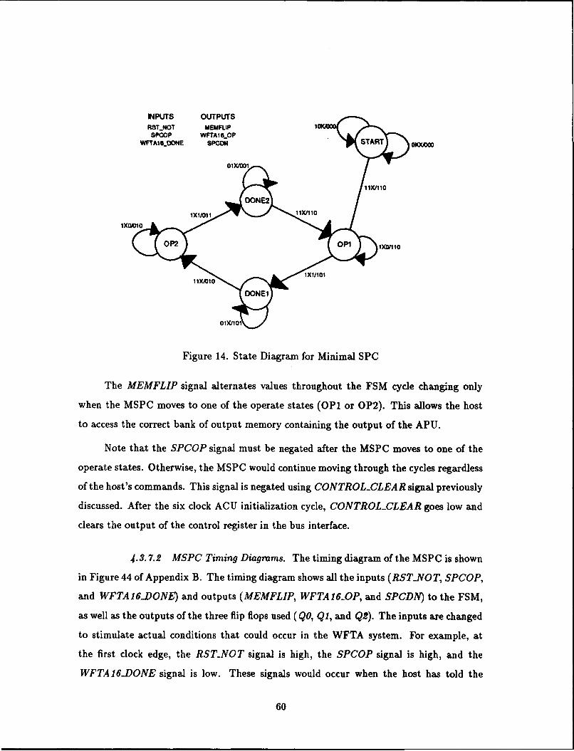
INPUTS OUTPUTSRSTNOT MEMFLIP 1CKJOOOSPCOP WFTA16-OP
WFTAISDONE SPCON START0
FD11X/110
IXI/011 11X/110
OP2C 1mp0T110
11X7910 X1/101
01X/101
Figure 14. State Diagram for Minimal SPC
The MEMFLIP signal alternates values throughout the FSM cycle changing only
when the MSPC moves to one of the operate states (OP1 or OP2). This allows the host
to access the correct bank of output memory containing the output of the APU.
Note that the SPCOP signal must be negated after the MSPC moves to one of the
operate states. Otherwise, the MSPC would continue moving through the cycles regardless
of the host's commands. This signal is negated using CONTROL-CLEAR signal previously
discussed. After the six clock ACU initialization cycle, CONTROL-CLEAR goes low and
clears the output of the control register in the bus interface.
4.3.7.2 MSPC Timing Diagrams. The timing diagram of the MSPC is shown
in Figure 44 of Appendix B. The timing diagram shows all the inputs (RSTNOT, SPCOP,
and WFTA16-DONE) and outputs (MEMFLIP, WFTA16_OP, and SPCDN) to the FSM,
as well as the outputs of the three flip flops used (QO, Q1, and Q2). The inputs are changed
to stimulate actual conditions that could occur in the WFTA system. For example, at
the first clock edge, the RSTNOT signal is high, the SPCOP signal is high, and the
WFTA16-DONE signal is low. These signals would occur when the host has told the
60
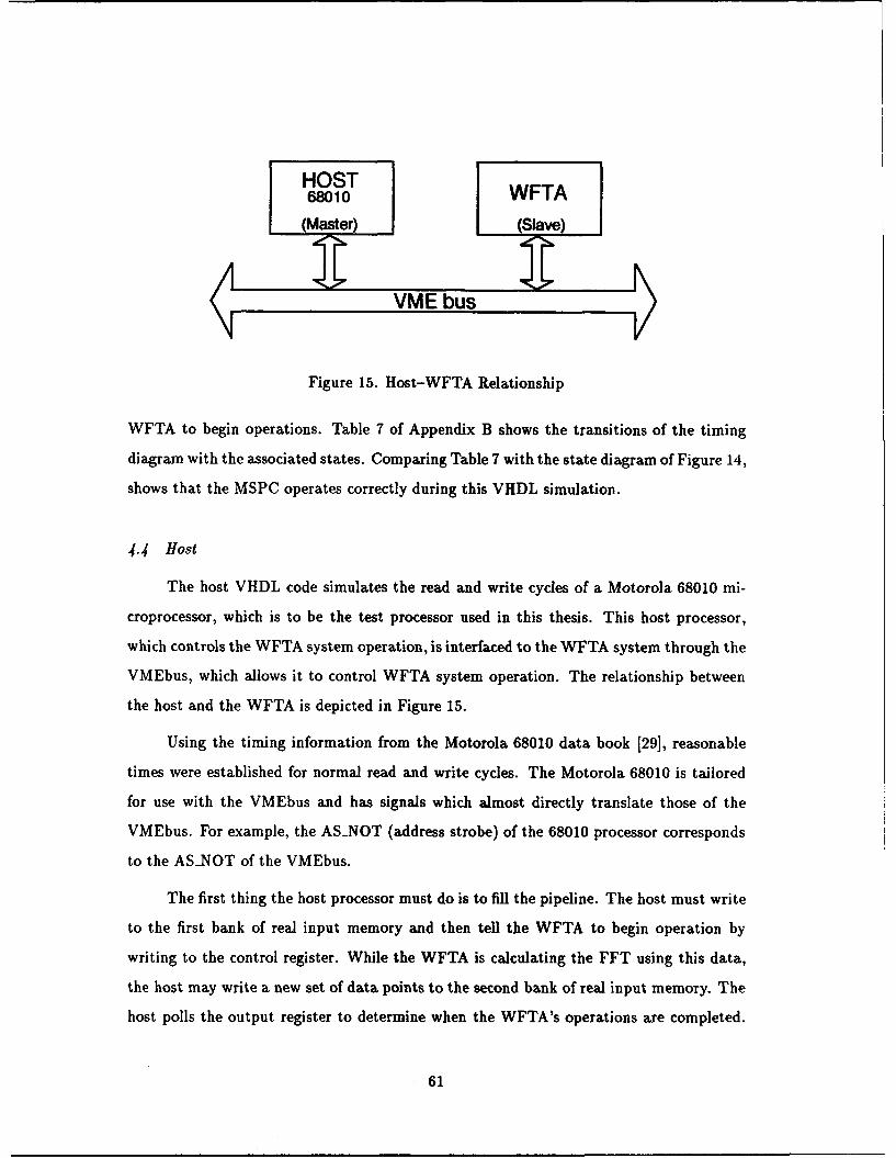
HOST68010 WFTA
(Master) (Slave)
VME bus
Figure 15. Host-WFTA Relationship
WFTA to begin operations. Table 7 of Appendix B shows the transitions of the timing
diagram with the associated states. Comparing Table 7 with the state diagram of Figure 14,
shows that the MSPC operates correctly during this VHDL simulation.
4.4 Host
The host VHDL code simulates the read and write cycles of a Motorola 68010 mi-
croprocessor, which is to be the test processor used in this thesis. This host processor,
which controls the WFTA system operation, is interfaced to the WFTA system through the
VMEbus, which allows it to control WFTA system operation. The relationship between
the host and the WFTA is depicted in Figure 15.
Using the timing information from the Motorola 68010 data book [29], reasonable
times were established for normal read and write cycles. The Motorola 68010 is tailored
for use with the VMEbus and has signals which almost directly translate those of the
VMEbus. For example, the AS-NOT (address strobe) of the 68010 processor corresponds
to the AS-NOT of the VMEbus.
The first thing the host processor must do is to fill the pipeline. The host must write
to the first bank of real input memory and then tell the WFTA to begin operation by
writing to the control register. While the WFTA is calculating the FFT using this data,
the host may write a new set of data points to the second bank of real input memory. The
host polls the output register to determine when the WFTA's operations are completed.
61
When they are complete, the host must tell the WFTA system to begin the operation
a second time so the output memory bank switches for the host to read. To maximize
throughput on the system, the host must read the output memory during the time that
it takes the APU to calculate a FFT and, if additional points are necessary, load the real
memory input. Then the polling process starts again.
The important point here is the host must tell the WFTA system to operate one
last time to read the last set of output data. When the WFTA has completed an FFT,
the FFT data in the output memory is oriented toward the APU and not toward the
VMEbus. There is no way for the host to access the output data. Telling the WFTA
to start again, flips the memory and orients the memory bank that holds the FFT data
toward the VMEbus and the host. The host can now access the data and read it out to
the host memory. This means that "garbage" data was input to the APU and output to
the memory. However, this is the only way to get data from the output memory.
The host VHDL code does not reflect the entire handshaking protocol used in the
data transfer functions of the VMEbus. The behavioral description of the 68010 is by no
means complete, but it is complete enough to provide the WFTA system with the required
signals from the VMEbus so that the system can be demonstrated.
Apart from the VHDL behaviorial description, two files are necessary for proper
operation (the data input file and the data output file). The code reads data from an
input file called "fourier-input" and writes data to an output file called "fourier.output".
The complete VHDL code for the host is located in Appendix K of this thesis.
4.5 Test Plans
The design process is typically an iterative process, with each step of the process being
tested to be sure each design entity is checked with a "test bench" used to demonstrate
the entity was operating correctly. Each level of hierarchy was tested and results validated
before continuing on to the next level of design. An independent tester should be able to
reproduce the results of this thesis with these test benches. Table 5 lists the test benches
used against each particular entity.
62
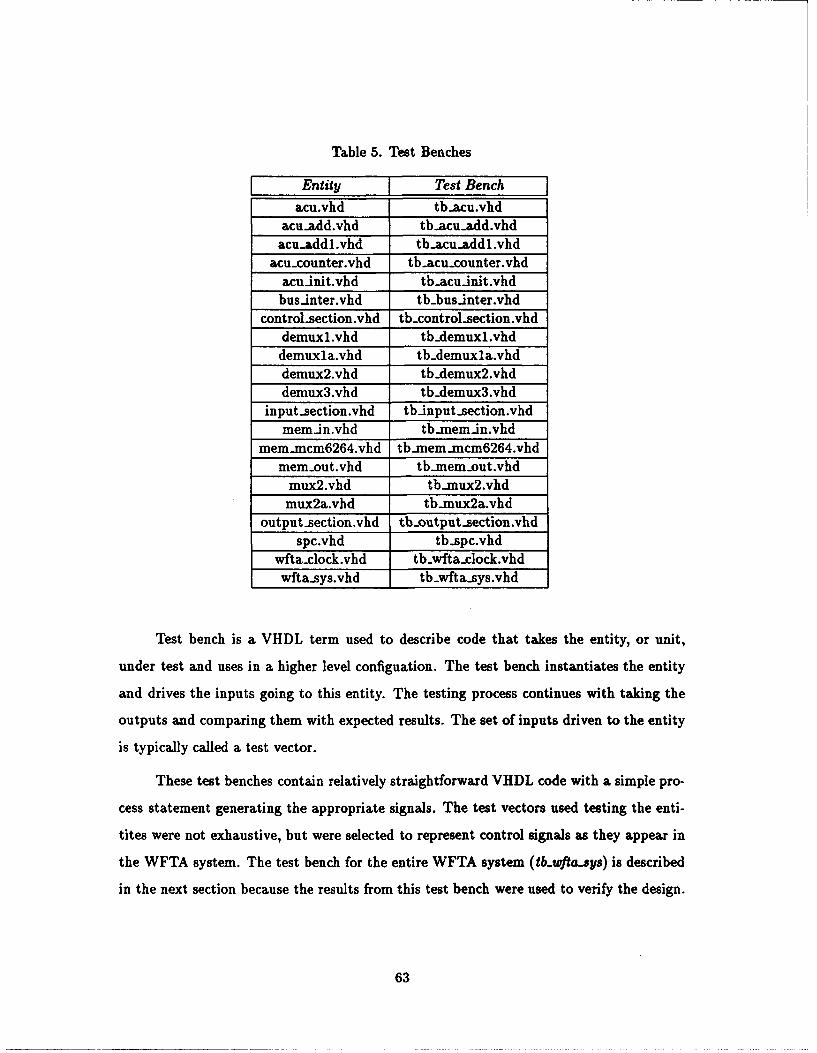
Table 5. Test Benches
Entity Test Bench
acu.vhd tb..acu.vhdacu..add.vhd tb..acuadd.vhd
acu-addl.vhd tb.acu.-addl.vhda cu.counter.vhd tb.acu-counter.vhd
acuinit.vhd tb.acu-init.vhdbus-inter.vhd tb.bus-inter.vhd
control.section.vhd tb control-section.vhddemuxl.vhd tb-demuxl.vhddemuxla.vhd tb-demuxla.vhddemux2.vhd tb.demux2.vhddemux3.vhd tb-demux3.vhd
input-section.vhd tb-input-section.vhdmemin.vhd tbamem.in.vhd
mem-mcm6264.vhd tb.mem-mcm6264.vhdmemrout.vhd tb.mem-out.vhd
mux2.vhd tbjmux2.vhdmux2a.vhd tbamux2a.vhd
output section.vhd tb-output..section.vhdspc.vhd tb.spc.vhd
wfta-clock.vhd tbkwfta.clock.vhdwfta.sys.vhd tb.wfta-sys.vhd
Test bench is a VHDL term used to describe code that takes the entity, or unit,
under test and uses in a higher level configuation. The test bench instantiates the entity
and drives the inputs going to this entity. The testing process continues with taking the
outputs and comparing them with expected results. The set of inputs driven to the entity
is typically called a test vector.
These test benches contain relatively straightforward VHDL code with a simple pro-
cess statement generating the appropriate signals. The test vectors used testing the enti-
tites were not exhaustive, but were selected to represent control signals as they appear in
the WFTA system. The test bench for the entire WFTA system (tb.wfta-sys) is described
in the next section because the results from this test bench were used to verify the design.
63
Prior to testing a particular entity, both the file containing the entity and the test
bench, in that order, must be re-analyzed using the Synopsys package. This re-analysis is
necessary because the test benches use the same entity name, the same architecture, and
the same configuration declaration for the testbench. Therefore, the simulation file that
is created for each test bench has the same name and overwrites the simulation file that
existed prior to the re-analysis.
The complete VHDL code for all the test benches and results using the trace option
in the simulator are located in Appendix K of this thesis. Some of the results of the test
benches were used to illustrate the design and can be found in Appendix B.
4.6 Evaluation of VHDL Development
The first two objectives of this thesis, the design of a VMEbus interface and devel-
opment of VHDL code describing the WFTA system were incorporated into this chapter,
because they were closely tied to each other. This section evaluates the two objectives
jointly. The design of the WFTA system was completed and provides a platform for the
testing and proof of concept for the WFTA16 processor in a total system. Using a chip-
level VHDL simulation which directly reflects the design of the WFTA system, the design
was validated for several test cases.
The test bench for the entire WFTA system (tb-wfta-sys) was different in structure
from the other test benches. Instead of a process statement, the host VHDL code was
inserted. This test bench models the physical configuration that the WFTA would normally
use, with the host processor controlling the WFTA system. Since this closely models the
physical world, the results from this test bench simulation were used to verify the system
design.
4.6.1 Input Test Vector Selection. The first test vector used in verifying the system
design was the sixteen points representing a 1 Hz sine wave. This signal was used because
both the inputs and outputs were available from previous theses. The inputs used are
shown in Table 8 of Appendix C. Since this is a real signal, the input imaginary points are
64
all zero and the imaginary input test vectors are not shown. This models the imaginary
inputs to the APU being grounded in the design.
4.6.2 Simulation of the WFTA System. Using the single test vector for a 1 Hz sine
wave, the entire WFTA system was simulated. The timing diagram generated for the
WFTA system is not shown in its entirety because the simulation took approxiamately
80000 ns. Rather, sections of the timing diagram have been extracted to verify that the
design of the WFTA system operates correctly. The timing diagrams used in the discussion
of this section are shown in Appendix D.
Since it is impractical to trace every signal in the WFTA system simulation, the
correct data flow can be used to verify the design. Furthermore, the data can be easily
traced around the entire system. For specific details of the data flow when it enters one
of the major functional blocks, refer to the appropriate section in this chapter. Figure 45
shows the host writing the 16 data points to the input memory. The first address shown,
70001Eh (VME..ADD), is actually for the sixteenth point of data because the host VHDL
code writes the data in reverse order. The address 70000Fh might have be expected, but
the VMEbus is byte addressable while the WFTA system is word addressable. Each point
of data takes two bytes (one word). The address 70001Eh corresponds to the sixteenth
word in the input memory. The address from the VMEbus interface going to the input
memory is WRITE..ADD and the data from the VMEbus interface going to the input
memory is RL1. Although the host VHDL code writes the data to the input memory in
reverse order, with the sixteenth data point written first to the sixteenth location in the
input memory, the data is accessed in ascending order through the WFTA system. The
first data point assessed by the ACU is located in the first location in the input memory.
After the host is finished with loading the input data, the host tells the WFTA to begin
operation by writing to 704000h which corresponds to the control word register. Notice
that SPCOP goes high and MEMFLIP changes from low to high. The MEMFLIP must
change so that the input data is oriented towards the APU. Also notice that SPCOP goes
low after a short time. This is caused by the CONTROL-CLEAR signal from the ACU
which clears the control word register.
65
Figure 46 shows the ACU addressing the input memory and data flowing to the APU.
The addresses generated by the ACU are IN-ADD, in ascending order, and the data from
the the input memory to the APU is RL*. The VMEbus addresses (VME.ADD) can be
disregarded. The VHDL host code is simply loading another set of data points in the input
memory demonstrating the pipelining features of this design.
Figure 47 shows the ACU addressing the output memory and data flowing from the
APU to the output memory. The addresses generated by the ACU axe OUT-ADD, in
ascending order. The real FFT data from the APU to the output memory is RO_1, which
corresponds to the actual real output test vectors of Table 9 of Appendix C. The imaginary
FFT data from the APU to the output memory is 10-1, which corresponds to the actual
imaginary output test vectors of Table 10 of Appendix C. Notice that both ROI and
10-1 are 24-bits wide coming from the APU to the output memory and the table entries
of Tables 9 and 10 are 16-bits wide. The 16 most significant digits of the RO-1 and 10-1
data busses are the bits that compare to the table entries. Although the design decision
was made to change the datapath from 24-bits to 16-bits in Section 3.3, the APU still
outputs 24-bits of FFT data.
When the ACU and APU are finished loading the output memory, the SPCDN signal
goes from low to high, telling the host that the WFTA has completed the FFT. The host
VHDL code is not polling at this time because there is a busy loop in the VHDL code
which executes prior to polling the output word register.
Figures 48, 49, 50, and 51 shows the host reading the output memory for the FFT
data. The VMEbus address (VMEADD), 708000h, maps to the output word register.
The host, which has been in a busy loop, only polls once because the WFTA has already
completed the FFT. When the host determines that the WFTA is finished, the host tells
the WFTA to calculate another FFT by writing to the control word register (704000h).
This write operation orients the data in the output memory towards the host. Notice that
the MEMFLIP signal goes from high to low. The host then reads the output memory.
The host code alternates reading the output memory, first reading from the real output
memory (70CO00h), and then reading from the imaginary output memory (70E000h). The
host reads the 16 points of real FFT data and 16 points of imaginary FFT data. The
66
address from the VMEbus interface going to the output memory is READ-ADD. The data
going from the output memory to the VMEbus interface is RO.2 for the real FFT data
and 10-2 for the imaginary FFT data.
4.6.3 Results of WFTA System VHDL simulation. The host takes the FFT data
from the output memory and writes them into a file (fourier.output). The results from
the VHDL simulation were compared to the expected FFT values. This comparison is
shown in Tables 9 and 10 of Appendix C. The WFTA system VHDL simulation results
are exactly the same as the expected values. Similar tests to the one described above were
conducted on a 1 Hz cosine wave, a 2 Hz sine wave, and a 2 Hz cosine wave. In all these
tests, the results from the simulation matched the expected values. The WFTA system
design was verified in VHDL using the results from these simulations.
4.7 Summary
This chapter has covered the VHDL development for the WFTA system described
in Chapter III. The design of each of the major functional blocks is discussed in detail.
Behavioral VHDL descriptions of integrated circuits were developed and used as the basic
building blocks of the structural VHDL description of the WFTA sytem down to the
integrated circuit level. Through the use of a set of comprehensive test benches, the design
was verified for correct operation in simulation. A rudimentary model of the host processor
in VHDL was developed to simulate the control signals from the host to the WFTA system
via the VMEbus. The next chapter describes the WFTA system construction.
67
V. Construction of the WFTA System
5.1 Introduction
There is a tremendous difference between a paper design and actually wirewrapping
chips to a VMEbus breadboard. The physical world has such things as capacitance, current
drive requirements, fan-in, and fan-out. Rarely are signals as "clean" in VHDL as they are
in the digital lab. Although VHDL can be made to account for these physical actualities,
the VHDL design becomes more intricate and complicated. Lack of time during this thesis
cycle made modelling these physical considerations impractical.
Furthermore, a design developed in VHDL is only as good as the behavioral descrip-
tions that form the foundation of the simulation. Actually, the behavioral descriptions are
not complete in that they do not totally reflect the ideal specifications of the datasheets.
Differences in expected behavior versus actual behavior can often result in errors in the
construction. This was the case in this thesis, which resulted in changes to the VHDL
model to reflect actual behavior observed.
These two factors forced the design of the system to be modified during this phase
of the thesis. Errors not detected during VHDL development manifested themselves in the
actual construction. One example of this modification was the elimination of a latch used
in the original design between the VMEbus interface and the input memory. Although the
original design would have worked with the latch, the elimination of the latch decreased
the chip count, which was critical during the entire design. As stated previously, the design
that was discussed in Chapter IV represents the final design describing the device after all
the design iterations.
Since the drqign of the WFTA system has already been discussed in Chapter IV, this
chapter deals wit,. he specifics of the equipment and procedures used in the digital lab
and other documentation that will help clarify and continue any future work in this area.
The same schematics used in the VHDL development also document the construction
phase of this thesis. The schematic produced with the Synopsys SGE tool provides the
ability to label pin and chip numbers. There is no single level schematic with contains all
68
the gates and connections. Rather, the schematics are hierarchical. As mentioned before,
all the schematics used for this design axe located in Appendix K of this thesis.
Due to time and resource constraints, the WFTA system described by Chapter IV
was not completely built. The input memory and MSPC functional blocks were totally
completed along with a partial construction of the VMEbus interface.
This chapter starts with a discussion of the resources used in the construction, fol-
lowed by a section on the construction methodology and the testing procedures for those
blocks that were built. Then specific problems concerning construction are discussed,
followed with an evaluation of this phase of the thesis against the stated objective.
5.2 Resources
The following sections discusses some of the peculiar resource requirements for the
WFTA prototype system that was assembled in the digital lab. Specific equipment and
tools used are discussed first, followed by the types of integrated circuits composing the
system. Additionally, there were many parts needed particular to wirewrapping and the
VMEbus. Whenever possible, the make, model, or part number is listed in the discussion.
5.2.1 Equipment and Tools. The chassis used for this thesis which contains the
VMEbus backplane was the MVME945-1 Chassis from Motorola Incorporated. All the
specifications for this chassis are discussed in the User's Manual [32]. Usually, the 945
chassis contains one 12-slot, full 32-bit VMEbus backplane using the bus connectors P1
and P2 to connect to the bus lines. However, the version used for this thesis only contained
the P1 connector on the backplane, forming a 16-bit VMEbus backplane. Using this chassis
to hold particular VMEbus cards, total processing systems can be implemented onto the
backplane.
One of the cards used in this thesis is the processor card or MVME120, VMEbus
Microprocessor Module, produced by Motorola [33]. The microprocessor used in this card
is the Motorola 68010. However, this entire VMEbus card houses a complete processor
system with RAM, ROM, interrupt handler, and bus requester. This was the host processor
discussed in previous chapters of this thesis. The other VMEbus card used in the chassis
69
was the controller card, MVME050, also produced by Motorola. This card assumes the
duties of bus master upon power up and arbitrates bus requests on the VMEbus. This
controller card must be used in conjunction with the MVME120, Microprocessor Module,
as it also provides the power, ground and clock used on the VMEbus.
The most important tool used during the testing of this phase was the HP-1631A/D
logic analyzer produced by Hewlett Packard [34]. The logic analyzer is general purpose
machine capable of performing state, timing, and analog waveform measurements. For
this thesis, the logic analyzer was used for making only digital timing measurements. The
logic probes were attached to specific signals and the waveforms were compared with the
expected results from the VHDL development.
In order to communicate with the Motorola 68010 on the MVME120 VMEbus card
a dumb terminal with RS232 interface was needed. The terminal used for this thesis was
the Heath H-29 Video Display Terminal [35]. The RS232 interface is located on the front
of the MVME120 Microprocessor Module. This terminal provides input/output functions
from the user to the resident debug monitor program in the MVME120 Microprocessor
Module. Without this monitor and keyboard, there is essentially no way for the user to
control the 68010 in the MVME120 card. The debug monitor is a ROM resident program
that acts a rudimentary operating system for the host 68010 [36].
5.2.2 Integrated Circuits. In construction of the actual WFTA system, the inte-
grated circuits were the most numerous resource and also the most difficult to acquire. In
total, there were 160 integrated circuits needed for this design which were obtained from
different sources.
In Table 1 of the last chapter, the type of chips used in this design were listed but
not broken down in any manner. In this chapter, the number and location of use for
these integrated circuit chips is important, and Table 6 provides a better indication of
this distribution between the different functional blocks. The total number of chips in the
previous paragraph is somewhat deceiving since some of the chips have more than one
gate in the package. For example, the SN74LS04 inverter gate has six inverters on a single
70
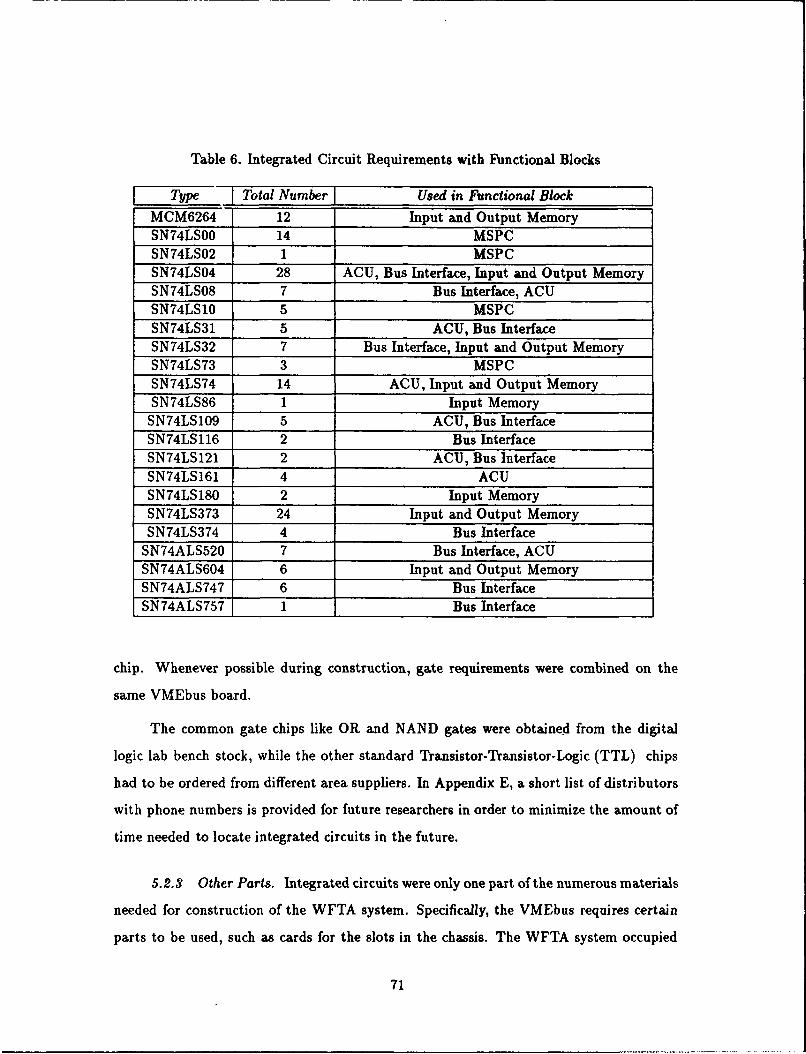
Table 6. Integrated Circuit Requirements with Functional Blocks
Type Total NumberJ Used in Functional Block
MCM6264 12 Input and Output MemorySN74LSOO 14 MSPCSN74LS02 1 MSPCSN74LS04 28 ACU, Bus Interface, Input and Output MemorySN74LS08 7 Bus Interface, ACUSN74LS10 5 MSPCSN74LS31 5 ACU, Bus InterfaceSN74LS32 7 Bus Interface, Input and Output MemorySN74LS73 3 MSPCSN74LS74 14 ACU, Input and Output MemorySN74LS86 1 Input Memory
SN74LS109 5 ACU, Bus InterfaceSN74LS116 2 Bus InterfaceSN74LS121 2 ACU, Bus InterfaceSN74LS161 4 ACUSN74LS180 2 Input MemorySN74LS373 24 Input and Output MemorySN74LS374 4 Bus Interface
SN74ALS520 7 Bus Interface, ACUSN74ALS604 6 Input and Output MemorySN74ALS747 6 Bus InterfaceSN74ALS757 1 Bus Interface
chip. Whenever possible during construction, gate requirements were combined on the
same VMEbus board.
The common gate chips like OR and NAND gates were obtained from the digital
logic lab bench stock, while the other standard Transistor-Transistor-Logic (TTL) chips
had to be ordered from different area suppliers. In Appendix E, a short list of distributors
with phone numbers is provided for future researchers in order to minimize the amount of
time needed to locate integrated circuits in the future.
5.2.3 Other Parts. Integrated circuits were only one part of the numerous materials
needed for construction of the WFTA system. Specifically, the VMEbus requires certain
parts to be used, such as cards for the slots in the chassis. The WFTA system occupied
71
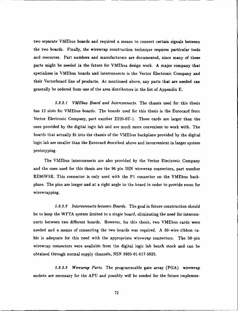
two separate VMEbus boards and required a means to connect certain signals between
the two boards. Finally, the wirewrap construction technique requires particular tools
and resources. Part numbers and manufacturers are documented, since many of these
parts might be needed in the future for VMEbus design work. A major company that
specializes in VMEbus boards and interconnects is the Vector Electronic Company and
their Vectorboard line of products. As mentioned above, any parts that are needed can
generally be ordered from one of the area distributors in the list of Appendix E.
5.2.3.1 VMEbus Board and Interconnects. The chassis used for this thesis
has 12 slots for VMEbus boards. The boards used for this thesis is the Eurocard from
Vector Electronic Company, part number E220-6U-1. These cards are larger than the
ones provided by the digital logic lab and are much more convenient to work with. The
boards that actually fit into the chassis of the VMEbus backplane provided by the digital
logic lab are smaller than the Eurocard described above and inconvenient in larger system
prototyping.
The VMEbus interconnects are also provided by the Vector Electronic Company
and the ones used for this thesis are the 96 pin DIN wirewrap connectors, part number
RE96WSR. This connector is only used with the PI connector on the VMEbus back-
plane. The pins are longer and at a right angle to the board in order to provide room for
wirewrapping.
5.2.3.2 Interconnects between Boards. The goal in future construction should
be to keep the WFTA system limited to a single board, eliminating the need for intercon-
nects between two different boards. However, for this thesis, two VMEbus cards were
needed and a means of connecting the two boards was required. A 50-wire ribbon ca-
ble is adequate for this need with the appropriate wirewrap connectors. The 50-pin
wirewrap connectors were available from the digital logic lab bench stock and can be
obtained through normal supply channels, NSN 5935-01-017-5825.
5.2.3.3 Wirewrap Parts. The programmable gate array (PGA) wirewrap
sockets are necessary for the APU and possibly will be needed for the future implemen-
72
tations of the ACU, memory, and MSPC. Different PGA sockets will be needed for the
different application specific chips. The staff of the digital logic design lab is searching for
PGA sockets for one of the design classes here at AFIT and at the time of this thesis, were
not successful in finding a company that provided these materials.
Additionally, wirewrap sockets for standard dual in-line package (DIP) integrated
circuits are needed but the digital logic lab has an adequate and fairly complete supply
of any of these sockets that might be necessary for any prototyping work. However, these
should be ordered as well since the digital logic laboratory needs these sockets for some of
the classes held there.
The wire and wirewrap tool is also available from the on-duty technician in the
digital logic lab. The wire used in wirewrapping is a standard AWG-30 gauge wire and the
wirewrap tool used for this thesis is produced by OK Industries, Incorporated, Yonkers,
New York, part number WSU-30M.
5.3 Partitioning of Functional Blocks
Considering the number of chips necessary to implement the design, there was no
other alternative than to use two VMEbus cards to house the WFTA system. With this in
mind, and knowing the space on the two VMEbus cards was limited, a plan was necessary
to partition the area of the boards to minimize the number of interconnecting wires required
between them.
The first consideration was ease of maintainability and any future work to be per-
formed with this board. The major functional blocks were kept together as much as
possible. For example, the VMEbus interface block was located on a specific area of one of
the boards. This makes replacement and modification of specific functional blocks easier.
The second consideration dealt with minimizing interconnecting wires between the two
boards. The 16-bit wide datapath for both the real and imaginary datapaths, had to be
contained on one board.
These two considerations essentially solves the problem of the partitioning, by forcing
the VMEbus interface, input memory, output memory and APU blocks to be restricted to
73
VME Boardi VME Board2apC-OP mo
_ _D _______m LN
WoTArrAIS •oDONE
L I OUTPkrtA0OAE8W-7o)
NOTE: Al connectlns are throuo 0 ribbon c11 - betmn he boards.
Figure 16. Partitioning and Interconnect Signals
one VMEbus card as they form the FFT datapath. This leaves the two other blocks, the
ACU and the MSPC, to be constructed on the second VMEbus card. This separation is
shown in Figure 16 with the interconnecting control signals between the two boards.
5.4 Construction Methodology and Testing
The WFTA construction was built using a modular approach with the "piecewise"
testing of the prototype in mind. The number of inputs to the different modules made
testing difficult in a modular fashion. Building testing circuitry would be as involved as
building the actual system, and in the interest of time, this was not the testing method-
ology used. Furthermore, the availability of integrated circuits limited the sequence of
construction. So, alternatively, using the host processor as the starting point and as the
major testing apparatus, the WFTA system was built incrementally away from the host
following the datapath of the architecture. Each step of the construction must be verified
for proper operation before continuing to the next incremental step.
Starting with the input and control section of the bus interface, these functional
blocks were built and tested before continuing on to the input memory. Then by continuing
on the datapath, the input memory was built and tested to determine if the host was able
to write to the input memory. The next functional block built was the MSPC to provide
some of the control signals that were hardwired in the previous steps. The ACU, output
74
memory, and output section of the VMEbus interface were left for last in the construction,
but were not completed due to time and resource constraints. The specific chip location
and layout of the components on the two VMEboards is shown in Appendix F. These
figures represent the extent of the construction of the WFTA system.
At each step of the incremental construction, tests were performed to insure proper
operation before continuing on to the next step. However, this testing process was different
for each one of the steps. For example, for the first step of constructing the input and
control section of the VMEbus interface, the decoding signals and data lines were moni-
tored. The second step of constructing the input memory, however, required some of the
control lines of the input memory to be hardwired while the host processor wrote to the
input memory. Then, the input signals to the memory chips, such as the write enable and
data lines were monitored to insure proper operation. Since, the input memory could not
be read due to the lack of a datapath back to the VMEbus, monitoring the inputs to the
memory chip was the only way to verify operation. In the third and final step of construc-
tion, which was the MSPC, the WFTA16DONE signal was tied low. After writing the
control word, the output signals from the MSPC FSM were monitored to insure correct
operation.
As the main testing apparatus is the host processor, the commands of the Motorola
MVME-120 debug monitor were used [36]. In particular, the command used in the debug-
ging environment provided was the Memory Modify (M or MM) command, whose func-
tion is to change data values in memory. The format for the command is MM <address>
[;<options>] where the address is in hexadecimal. With certain options set, this command
can write a word to any location in the VMEbus address space. The first of the two mem-
ory change mode options that were needed was the ;W option which sets the size of the
memory modify to word length or 16 bits and the ;N option which is the no verification
option insuring that the debug monitor does not attempt to read data after updating. The
word length option is necessary because access to the WFTA system is only even byte
addressable. An example of this command is shown below.
MM 7000 ;W ;N
75
For each iteration of testing for this system, the memory modify command was used
to insure proper operation by writing to a memory location in the WFTA address space.
For example, writing to the control word started the finite state machine in the MSPC.
After writing to a particular location in memory, the HP-1631A/D logic analyzer was used
to monitor the important signals to insure expected behavior. The waveforms of significant
signals were compared to the expected results of the VHDL simulation. A component was
considered verified when the actual signals appeared similar to those predicted by VHDL.
This ad hoc procedure constituted the testing plan during the construction of the WFTA
system.
5.5 Specific Problems
There were are number of problems associated with the construction of the WFTA
system which are discussed in this section. These problems included the user interface
with the host, availiablity of parts, and the testing methodology.
5.5.1 Interface to Host. The host processor used for this WFTA system was Mo-
torola 68010 on the MVME120 Microprocessor Module card. The debug monitor program
in the ROM of the MVME120 is adequate for operation, but not extremely user-friendly.
In many ways the debug monitor is functionally limited, making the interface to the host
somewhat difficult. A different procedure will be used than the one discussed in this
chapter for the interactive testing when the host driver program is introduced in the next
chapter.
5.5.2 Parts. Although many of the chips and connectors were available in the dig-
ital lab, there were a number of uncommon items not currently stocked. Many of these
parts were ordered prior to construction; however, the design was not yet complete and un-
foreseeable chip requirements forced a quick search to find the needed components. Even
with last minute acquisitions, the parts list was not entirely fulfilled. This limited the
completion of the construction of the WFTA system before wire-wrapping the first chip
to the board.
76
5.5.3 Testing. The testing for this phase of the thesis was difficult because the
number of inputs and time constraints forced the use of the host processor in the testing
process. Construction was temporarily suspended for each test to insure correct operation
before continuing. Building a test circuit every time a module was completed would have
been prohibitive considering the time allocated for this effort.
5.6 Evaluation of Construction
The particular problems encountered during this phase of the thesis have already
been discussed in this chapter. As mentioned in the beginning of this chapter, the entire
WFTA system was not constructed onto VMEbus cards. The two major reasons for not
finishing were lack of resources and time. Even with the necessary resources, additional
time would be necessary to complete the WFTA system. Wirewrapping is a tedious and
time-consuming process. This fact, coupled with the constant testing at each phase of the
construction process, made assembling this prototype a prolonged process.
The parts of the WFTA system that were constructed and tested were the input and
control sections of the bus interface, the input memory and the MSPC. Up to this point,
the design was validated in actual hardware. However, before the entire WFTA system
can be validated as operational, the remaining functional blocks need to be installed and
tested-the output memories, the ACU, and the output section of the bus interface.
5.7 Summary
This chapter has covered the construction of the WFTA system in the digital logic
laboratory and focused on particular problem areas. The WFTA system described in
the design of Chapter IV was partially assembled and tested. The input memory and
MSPC functional blocks were completely built while the VMEbus interface block was only
partially built. Using the host processor as the primary testing apparatus, tests up to
this point of the construction have verified the VHDL design. The WFTA system was not
completed due to time constraints and a lack of resources. The next chapter deals with
the development of the host processor code that drives the WFTA system.
77
VI. Development of the Host Driver Code
6.1 Introduction
The system host processor has the important responsibility of maintaining the WFTA
pipeline and keeping it as full as possible. The program that performs this task is the host
driver program running on the host. In order to provide an environment which will test
and demonstrate the single WFTA processor, a rudimentary version of the host driver code
was developed for this thesis.
The host processor for this system was the Motorola 68010 16-bit microprocessor
located on the MVME-120 card of the VMEbus chassis. As already discussed in the last
chapter, input and output of data with the host processor is difficult for several reasons.
The processor itself has an embedded debug monitor with limited instruction set to control
the processor. Additionally, the chassis used for this design did not have a file system, and
any data which the FFT needs for calculation must be stored in system memory. This
I/O limitation has driven the host driver code developed for this thesis to perform a single
16-point FFT problem. With a more powerful host processor or a more user-friendly
environment, the pipelined nature of the WFTA system might be better exploited in the
software.
Another design decision for this work with respect to the software was to use the C
programming language for the host driver program. The major reason for this decision
was the only compiler available for the 68010 was the Aztec C Compiler by Manx Software
Systems, Inc. Another reason for this choice was in terms of software maintainability.
Given the resources, the only other choice would have been to write the program in 68010
assembler language, which in general is harder to read and understand and more difficult
to maintain.
This chapter discusses the development of the host processor code used to drive the
WFTA system. The compilation and downloading procedures are discussed in Appendix
refdownload. This is followed by a discussion of the pseudocode version of the code. A
section describing the data flow diagram is next and the chapter ends an evaluation of this
objective against the goals stated in Chapter I.
78
6.2 Compilation, Download, and Run Procedures
This section discusses the procedures developed for compilation of the C source code,
downloading to the host processor, and running the host driver program on the MVME-
120. These three procedures are detailed in Appendix G.
6.3 Pseudocode for the Host Driver Program
Actually, the general nature of the code for the host driver program has already been
discussed implicitly in Chapter IV on VHDL development, Section 4.4. In order to test the
structural VHDL developed for the WFTA system, the signals generated by the WFTA
system host had to be simulated. Essentially, the structure of the host driver program can
be derived from this behavioral description of the host processor by using the commands
necessary to create the simulated signals.
The pseudocode developed for the host driver program is listed in Figure 17. As
stated earlier, this pseudocode has been written to operate on data for only a single FFT.
The numbers located to the left of the statements in Figure 17 are associated with the
data flow diagrams discussed in the next section and can be disregarded temporarily.
The pseudocode is fairly straightforward. The first for loop reads a set of sixteen
points of data and writes that data into the input memory of the WFTA system. The
address used by the host for system memory was arbitrary until the address for the WFTA
was hardwired into the VMEbus interface. The memory for the WFTA must be from
address location 700000h to 70001Fh corresponding to the bottom sixteen addresses of the
input memory (the input memory is even-byte addressable) with the first data point going
in the zero address location. This address is mandatory because this address is hard-wired
into the VMEbus interface. The VMEbus and 68010 are both byte-addressable but each
set of points written to the input memory consists of a "word" with two bytes (16 bits),
therefore the first point of data is located at 700000h and the second point of data is
located at 700010h.
79
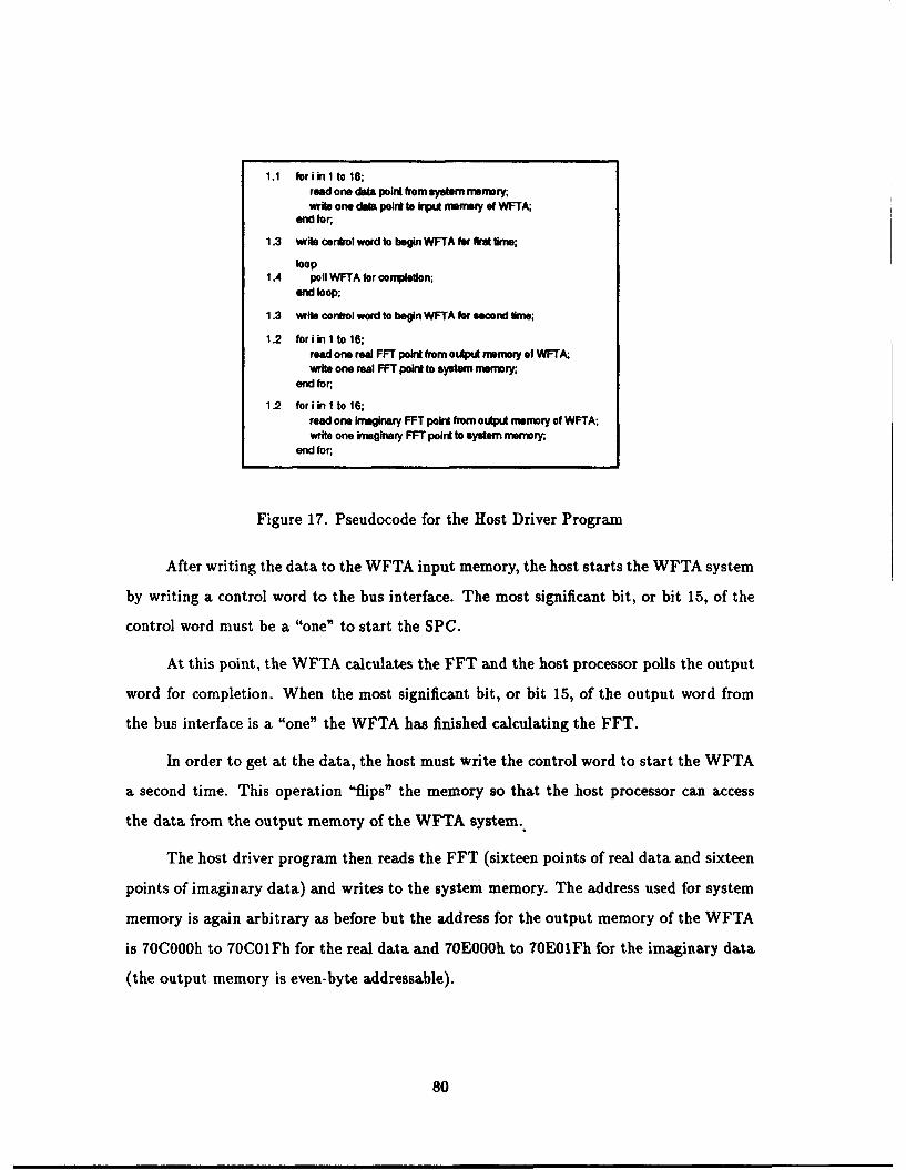
1.1 foriin to 16;read one data poirt from system memory;write one daba poirt to "nput rrmery of WFTA;
end for
1.3 write cer-ol word to begin WFTA for firt time;
loop1.4 poll WFTA for completion;
end loop;
1.3 write conrol word to begin WFTA for seoend time;
1.2 for iin I to 16;read one real FFT poirt from oiip.u nmmory of WFTA;write one real FFT poirt to system memory;
end for;
1.2 for iin I to 16;read one igminary FFT poirt from olpu memory of WFTA;write one imaginary FFT poirt to system memory,
end for;
Figure 17. Pseudocode for the Host Driver Program
After writing the data to the WFTA input memory, the host starts the WFTA system
by writing a control word to the bus interface. The most significant bit, or bit 15, of the
control word must be a "one" to start the SPC.
At this point, the WFTA calculates the FFT and the host processor polls the output
word for completion. When the most significant bit, or bit 15, of the output word from
the bus interface is a "one" the WFTA has finished calculating the FFT.
In order to get at the data, the host must write the control word to start the WFTA
a second time. This operation "flips" the memory so that the host processor can access
the data from the output memory of the WFTA system..
The host driver program then reads the FFT (sixteen points of real data and sixteen
points of imaginary data) and writes to the system memory. The address used for system
memory is again arbitrary as before but the address for the output memory of the WFTA
is 70C000h to 70CO1Fh for the real data and 70EOOOh to 70EO1Fh for the imaginary data
(the output memory is even-byte addressable).
80
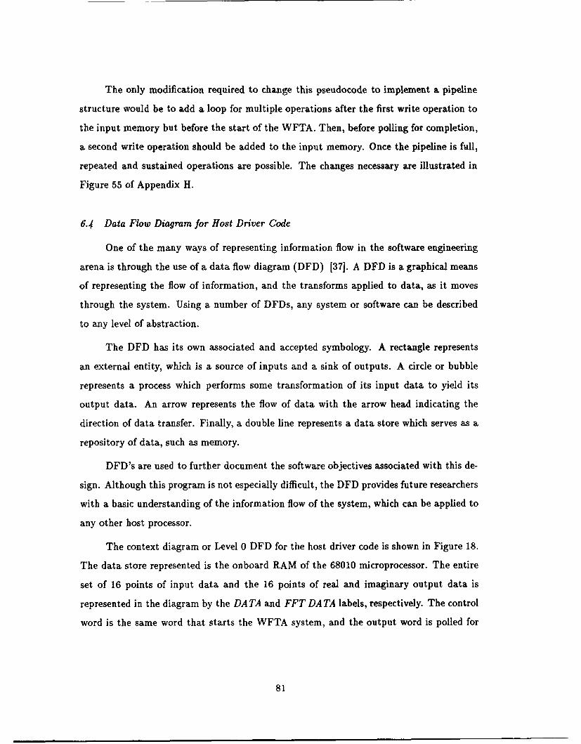
The only modification required to change this pseudocode to implement a pipeline
structure would be to add a loop for multiple operations after the first write operation to
the input memory but before the start of the WFTA. Then, before polling for completion,
a second write operation should be added to the input memory. Once the pipeline is full,
repeated and sustained operations are possible. The changes necessary are illustrated in
Figure 55 of Appendix H.
6.4 Data Flow Diagram for Host Driver Code
One of the many ways of representing information flow in the software engineering
arena is through the use of a data flow diagram (DFD) [37]. A DFD is a graphical means
of representing the flow of information, and the transforms applied to data, as it moves
through the system. Using a number of DFDs, any system or software can be described
to any level of abstraction.
The DFD has its own associated and accepted symbology. A rectangle represents
an external entity, which is a source of inputs and a sink of outputs. A circle or bubble
represents a process which performs some transformation of its input data to yield its
output data. An arrow represents the flow of data with the arrow head indicating the
direction of data transfer. Finally, a double line represents a data store which serves as a
repository of data, such as memory.
DFD's are used to further document the software objectives associated with this de-
sign. Although this program is not especially difficult, the DFD provides future researchers
with a basic understanding of the information flow of the system, which can be applied to
any other host processor.
The context diagram or Level 0 DFD for the host driver code is shown in Figure 18.
The data store represented is the onboard RAM of the 68010 microprocessor. The entire
set of 16 points of input data and the 16 points of real and imaginary output data is
represented in the diagram by the DA TA and FFT DATA labels, respectively. The control
word is the same word that starts the WFTA system, and the output word is polled for
81
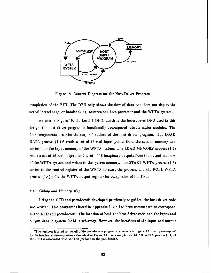
DATADATA
DATAATLMEMOR
FFTT DATA
Figure 18. Context Diagram for the Host Driver Program
,:<mpletion of the FFT. The DFD only shows the flow of data and does not depict the
actual interchange, or handshaking, between the host processor and the WFTA system.
As seen in Figure 19, the Level 1 DFD, which is the lowest level DFD used in this
design, the host driver program is functionally decomposed into its major modules. The
four components describe the major functions of the host driver program. The LOAD
DATA process (1.1)1 reads a set of 16 real input points from the system memory and
writes it to the input memory of the WFTA system. The LOAD MEMORY process (1.2)
reads a set of 16 real outputs and a set of 16 imaginary outputs from the output memory
of the WFTA system and writes to the system memory. The START WFTA process (1.3)
writes to the control register of the WFTA to start the process, and the POLL WFTA
process (1.4) polls the WFTA output register for completion of the FFT.
6.5 Coding and Memory Map
Using the DFD and pseudocode developed previously as guides, the host driver code
was written. This program is listed in Appendix I and has been commented to correspond
to the DFD and pseudocode. The location of both the host driver code and the input and
output data in system RAM is arbitrary. However, the locations of the input and output
'The numbers located to the left of the pseudocode program statements in Figure 17 directly correspondto the functional decompositions described in Figure 19. For example, the LOAD WFTA process (1.1) ofthe DFD is associated with the first for loop in the pseudocode.
82
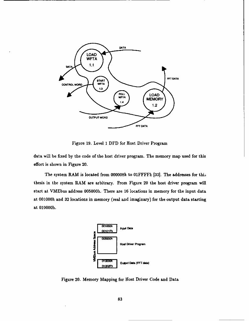
S~DATA
DMAT 1.1
START FFT DATA
CONTROL WORD WT
Figure 19. Level 1 DFD for Host Driver Program
data will be fixed by the code of the host driver program. The memory map used for this
effort is shown in Figure 20.
The system RAM is located from 000008h to 01FFFFh [33]. The addresses for thL•
thesis in the system RAM are arbitrary. From Figure 20 the host driver program will
start at VMEbus address 005000h. There are 16 locations in memory for the input data
at 00l000h and 32 locations in memory (real and imaginary) for the output data starting
at 010000h.
u •0(nFi U Data
EI IIHost Drvemr Program
Figure 20. Memory Mapping for Host Driver Code and Data
83
6.6 Testing and Evaluation of Host Driver Program Development
The host driver driver program was written in C and is listed in Appendix I. The
testing for the host driver code was not complete due to the unfinished construction of the
system and time constraints. In order to fully test this code, the entire WFTA system is
necessary to provide an environment which would react to coded instructions. The code
has been left for future researchers to modify and improve. The code listed in Appendix I
compiles but has not been run for this system. However, this program is simple enough
to insure that the code should work correctly. All the host driver code does is reads and
writes to addresses in the VMEbus address space.
6.7 Summary
This chapter has covered the development of the host processor code used to drive
the WFTA system along with other considerations involved with this particular VMEbus
system. The pseudocode and DFDs for the host driver program have been developed and
document the behavior of the host driver program. The code for the host driver was written
in C and compiles correctly but never tested due to time constraints. The next chapter
discusses the conclusions for the research and the recommendations for future research.
34
VII. Conclusions and Recommendations
7.1 Introduction
Every year, progress has been made toward VLSI chips that implements the Wino-
grad Fast Fourier Transform Algorithm. However, presently, there is a need for a platform
into which the WFTA16 processor could be demonstrated. This research was an effort to
solve that deficiency by designing and building a WFTA system that would provide an
environment for WFTA16 processor operation. Specifically, the overall goal of this thesis
was to design and build a working 16-point WFTA system that interfaces to the VMEbus
standard as a proof of concept for the WFTA system designed and developed at the Air
Force Institute of Technology.
In Chapter I, there were four objectives proposed to solve this problem. The first
was designing an interface between the WFTA system and VMEbus. The second was
developing VHDL code, down to the integrated circuit level, that implements the WFTA
system design. The third was constructing the WFTA system onto VMEbus cards. The
fourth was developing a host driver program to drive the WFTA system with data and
instructions. As described in the separate Evaluation sections in Chapters IV, V, and VI,
there were different levels of success with each of these objectives. This chapter presents
the conclusions and recommendations derived from the research described in this thesis.
7.2 Conclusions
Conclusions are drawn logically from research providing an indication of the overall
success of the solution to the problem statement. This section describes the conclusions
drawn from this research effort.
7.2.1 Validation of WFTA System Design. The WFTA system design, as described
in Chapter III and Chapter IV, was validated through VHDL simulations and tests con-
ducted during construction. The structural VHDL was developed to directly model the
WFTA system design down to the integrated circuit level. Appropriate timing of com-
ponents were included in this VHDL structural description. Using this description of the
85
WFTA system, simulation results showed that the WFTA correctly calculated the FFT for
a 1 Hz sine wave and other test signals. This simulation, along with results, are detailed
in Chapter IV. These results support the conclusion that the WFTA system design was
validated.
Although the construction was not complete, preliminary results indicate that the
actual hardware seems to match those expected from the VHDL simulation. The input
and control sections of the VMEbus interface, the input memory, and the MSPC were
the only functional blocks which were constructed. The testing results from the partial
construction further supports the conclusion of the WFTA system design validation.
Taking both the VHDL simulation results and partial construction results, the design
of the single processor WFTA system built for this thesis was validated.
7.2.2 Continued Work in the WFTA System. The work on the WFTA system needs
to be continued. The results of the partial construction of the WFTA system supports the
validation of the WFTA system design, but the entire system needs to be constructed to be
completely confident. Additionally, the host driver program was written but never tested.
These concerns indicate that continued research is necessary for the complete development
of a platform for the WFTA processors.
The architecture of the WFTA system used in this thesis is a scaled-down version of
the original WFTA design. It was meant to be used in a single processor configuration.
Research needs to be continued in the reconfigurable WFTA system architecture [2]. This
thesis was a good starting point for system design issues and provides a stable foundation
for continued work.
7.3 Recommendations
This section lists the recommendations for directions of further work or modifications
to the original design. These recommendations come from strictly a systematic view and
do not comment on the VLSI design of individual chips or original concept of design.
86
7.3.1 Further VLSI Work. One of the major problems with this thesis is there are
no commercially available chips for the major functional blocks of the WFTA system. For
example, for this thesis, there is no 16 X 16-bit word, dual-bank memory available which
can be read from one bank while at the same time providing access for writing to the
other bank. Consequently, using 8K X 8-bit chips in this design wasted a large amount of
memory. This lack of convenient commercial chips comes as no surprise since the original
WFTA design was based on a suite of application-specific integrated circuits. VLSI design
work needs to continue on the memory, ACU, and the SPC in conjuntion with the WFTA
processors.
Assuming a working APU, a priority list of the needed components can be described.
The first chip that needs to be fabricated is the ACU. This chip is closely tied to the
APU and the timing between the two devices is critical. The next chip needed would
be the memory chip which would greatly reduce the number of chips in the system. If
the jump is made to a reconfigurable WFTA system with two or more WFTA processors,
then the SPC must be the next chip fabricated. Building the SPC discretely for the more
complicated WFTA system would not be feasible because the number of integrated circuits
to implement the finite state machine would be prohibitive given the space constraints.
The recent AFIT acquisition of a field programmable gate array (FPGA) system will
make the fabrication of some of the components of the WFTA a simplified process. The
bus interface, the SPC, and the ACU could be constructed on a FPGA chip. This tool was
not available for this thesis but should provide future WFTA system designers with the
means to complete the system and significantly decrease the number of chips necessary.
7.3.2 Asynchronous Signals. Another problem is the lack of appropriate handshak-
ing signals between the different components of the WFTA system. As shown in this design,
some of the components will not necessarily be application specific and might have to be
constructed discretely from commercially available chips. The problem of timing is critical
and could be a significant problem when the actual WFTA16 processor is placed into the
empty space left on the breadboard from this design. Presently, the only synchronizing
signal between the two devices is the clock, the operate, and the done signal. There needs
87
to be additional asynchronous signals coming from the WFTA processor. When the actual
ASIC ACU is completed, then the additional signals might be unneccessary. But in the in-
terim, when using a discretely built ACU, additional signals might be beneficial and make
system design easier. One signal that would be useful is a "START WRITING" signal
which would indicate to the ACU when the WFTA processor is ready to start writing
output to the memory. Presently, the only way to establish this sychronization is for the
ACU to count a certain number of dock cycles before it outputs the addresses and the
write enable pulses.
7.3.3 Different Host. For this thesis, the host selection was not particularly im-
portant, since it was only dealing with a 16-point transform. However, when the full-up
WFTA is built, there needs to be a more powerful host processor driving the WFTA sys-
tem. Writing 16 points to memory before the WFTA16 processor is completed with a
previous set is not difficult using a 68010. But, looking toward the future, where the host
processor will write 4080 24-bit data words to memory, the WFTA would be "starved" for
data. Additional research into the WFTA project area needs to focus on an interface with
a faster and more powerful host processor and bus standard.
7.3.4 Behaviorial Descriptions of Chips. Using the behaviorial descriptions of the
chips used in the design of the WFTA system as a starting point, a library of behaviorial
descriptions of commercially available chips should be developed which can be used in the
future for any design work of a similar nature to this thesis. In fact, this library might
be coupled with the advanced microprocessor lab in order to prove designs in that lab
prior to actual construction. The SYNOPSYS package with its SGE environment has
eliminated much of the difficulty in VHDL design by providing configuration management
and stuctural construction from the behavioral descriptions.
7.3.5 Supply of Resources. A hardware thesis such as this one is difficult to com-
plete -t AFIT, not because of complexity of design but because of the lack of proper
support. For example, there was only one available VMEbus backplane for use in this the-
sis. Furthermore, many common ALS-series integrated circuits were unavailable and had
88
to be ordered or purchased. This deficiency has been corrected to some extent with the
purchase of a FPGA system, but there remains a problem. Supplies supporting a VMEbus
application should be stocked in the communications lab or digital lab if this standard is
to be used in future work. Although this might seem like "technician" work, an engineer
must be able to perform technical construction to a certain extent.
7.4 Lessons Learned
As discussed in this chapter, the objectives of Chapter I were not fully achieved.
However, the effort has provided future researchers with some lessons learned.
7.4.1 Scheduling of Construction. There was an underestimation of the time re-
quired for the construction of the WFTA system during this thesis. Construction on this
project started too late in the thesis cycle for completion. Do not make the same mistake
in the future. Allow at least two months for any hardware construction using the wirewrap
method. Resource shortcomings and testing will certainly fill this time. If an estimate is
made for construction, take the pessimistic view rather than the optimistic view.
7.4.2 Construction Methodology. The testing of this prototype forced a piecewise
construction methodology with functional blocks tested in system. Modular construction
and modular testing is much more desirable with any prototyping. Future work in con-
struction should use a modular approach, building the testing platforms necessary to fully
test the modules before including them in the complete system.
7.4.3 Ordering of Parts. Another problem tied to the construction problems dis-
cussed is the late ordering of parts needed for the design. Parts for this thesis were ordered
too late in the thesis cycle. Finish the design early enough to provide ample time for
parts to be ordered and shipped. Be aware of the end of the government's fiscal year when
funding for parts might become an issue.
89
7.5 Summary
This chapter has discussed the conclusions that were derived from this research,
the recommendations for the future direction of research in the WFTA project area, the
lessons learned during this thesis, and suggestions to improve the efficiency of hardware
development.
90
Appendix A. Schematics for Subcomponents
This appendix provides the schematics generated for the WFTA system design which
are discussed in Chapter IV. The schematics for the abstract, high-level functional blocks
are located in the thesis. The schematics in this appendix describe the subcomponents of
each of the major functional blocks of the WFTA system; the VMEbus interface, the input
and output memory, and the ACU. All these schematics were generated in the Synopsys
SGE environment.
91
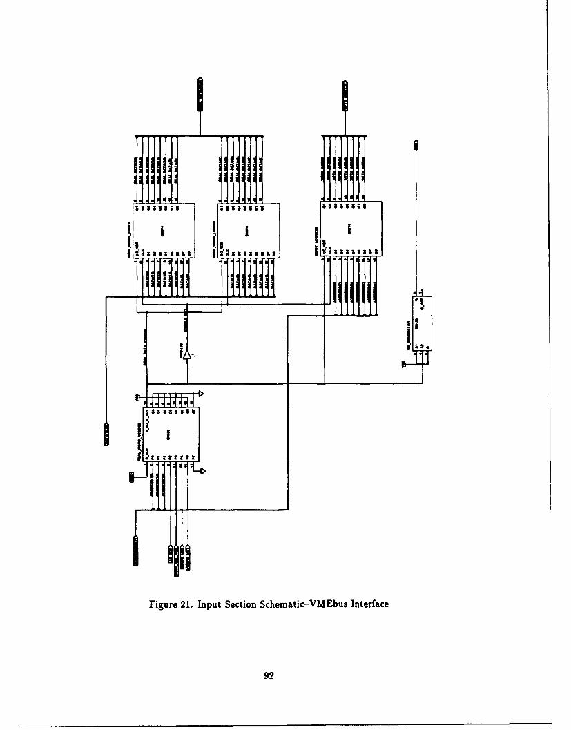
S~II 'II
- -
Figure 21. Input Section Schematic-VMEbus Interface
92
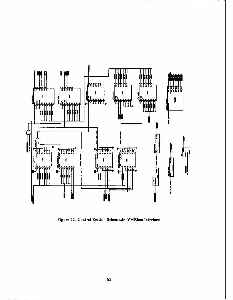
& i!asmset$ a a an
12213 stil
gas@&@
Figure 22. Control Section Schematic-VMEbus Interface
93
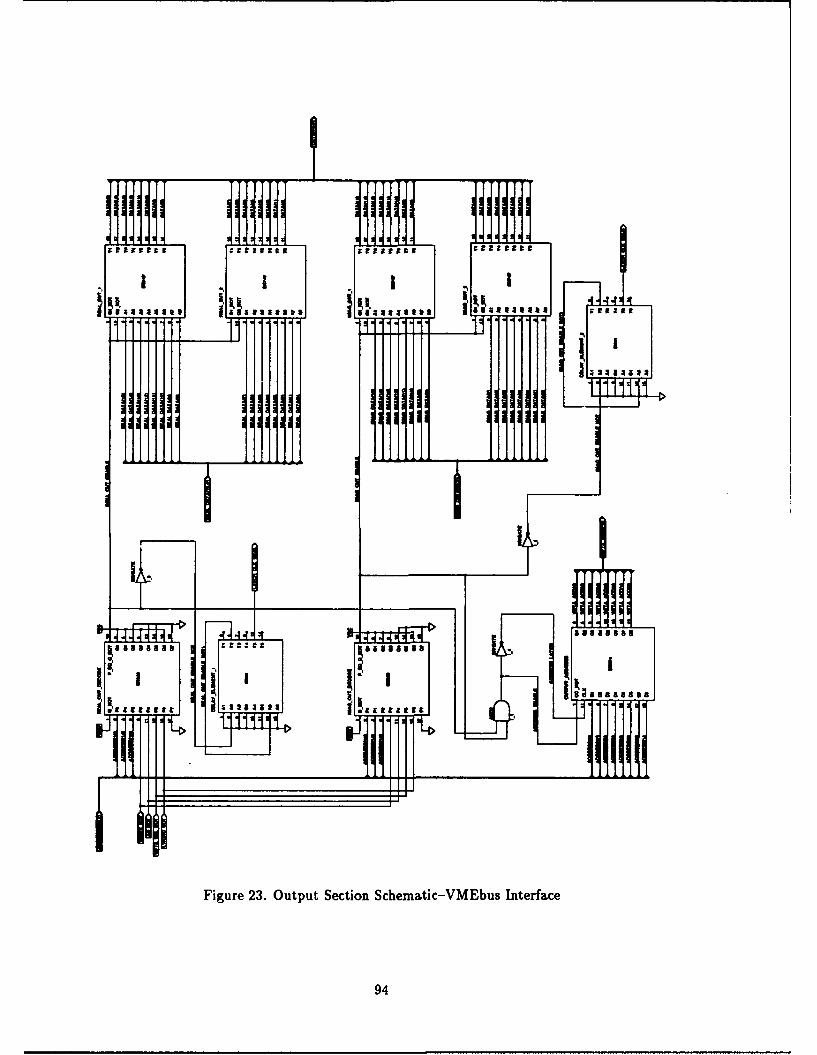
aIta91 t
Figure 23. Output Section Schematic-VMEbus Interface
94
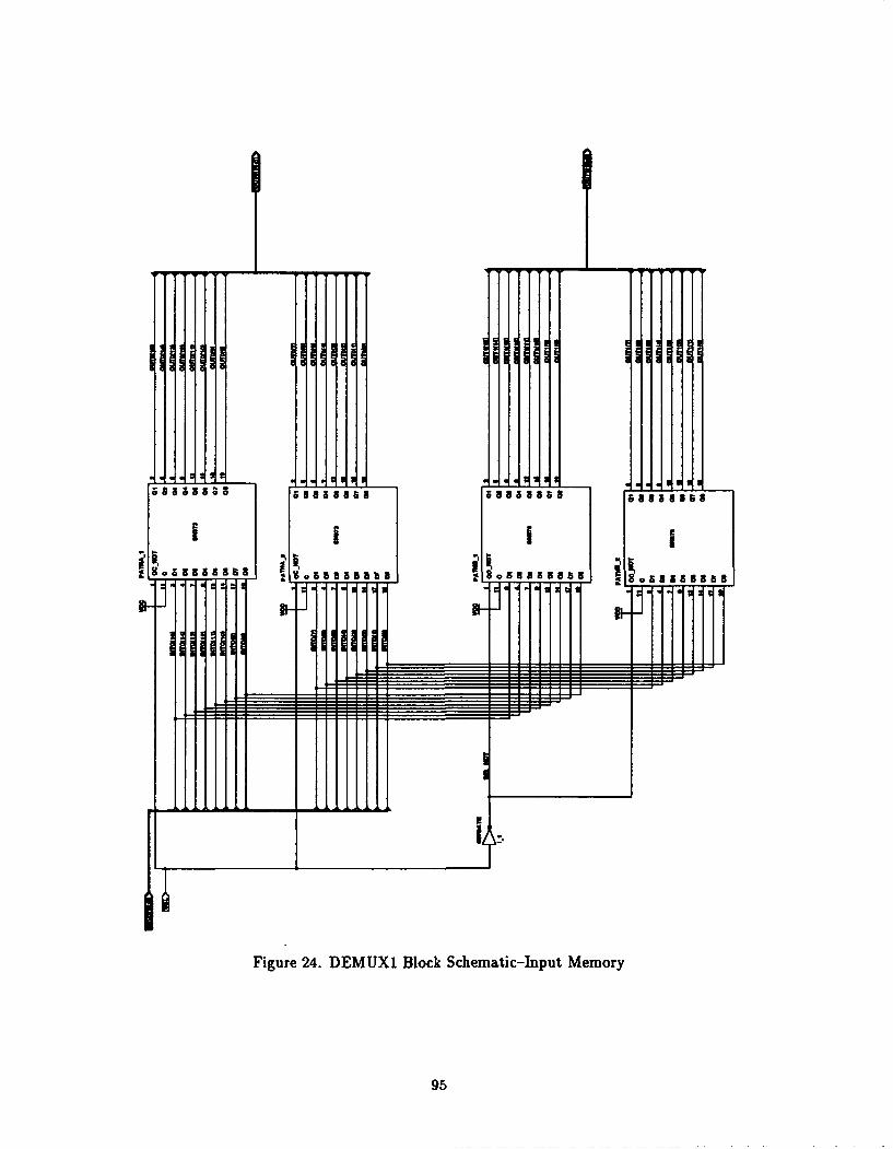
Iý4ý4 Iý4 J JI4j
Figure 24. DEMUXI Block Schematic-Input Memory
95
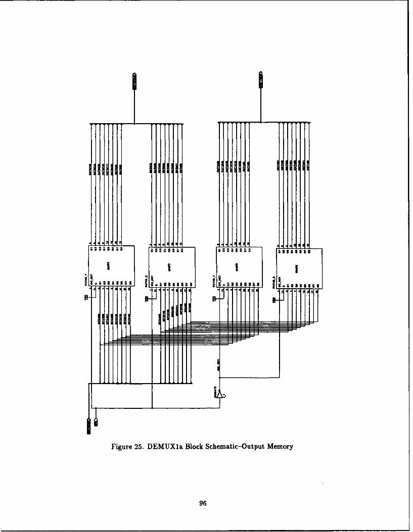
•, SSo 3~2~ Soi3I33SS $ 8 0 33$Saaz Il~S~
Figure 25. DEMUXia Block Schematic-Output Memory
96
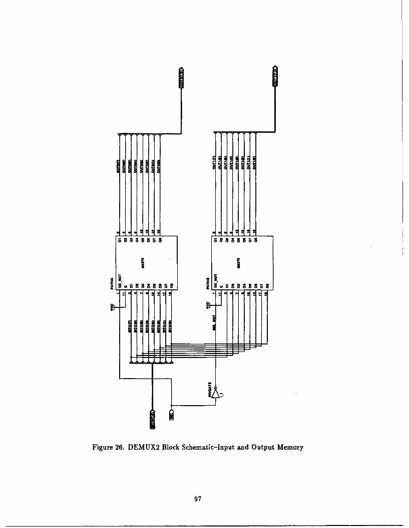
aI I
Figure 26. DEMUX2 Block Schematic-Input and Output Memory
97
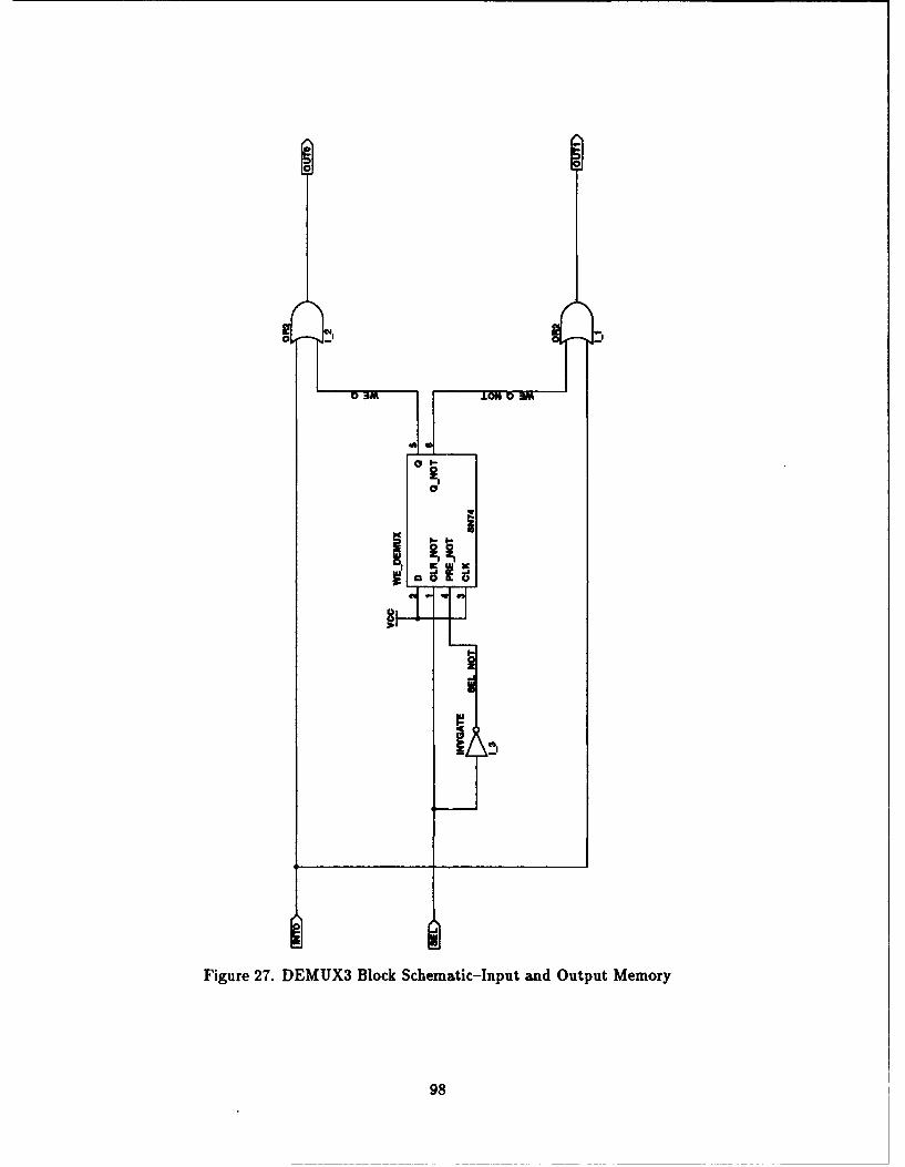
0
0 amIN0 0
i I
Figure 27. DEMUX3 Block Schematic-Input and Output Memory
98
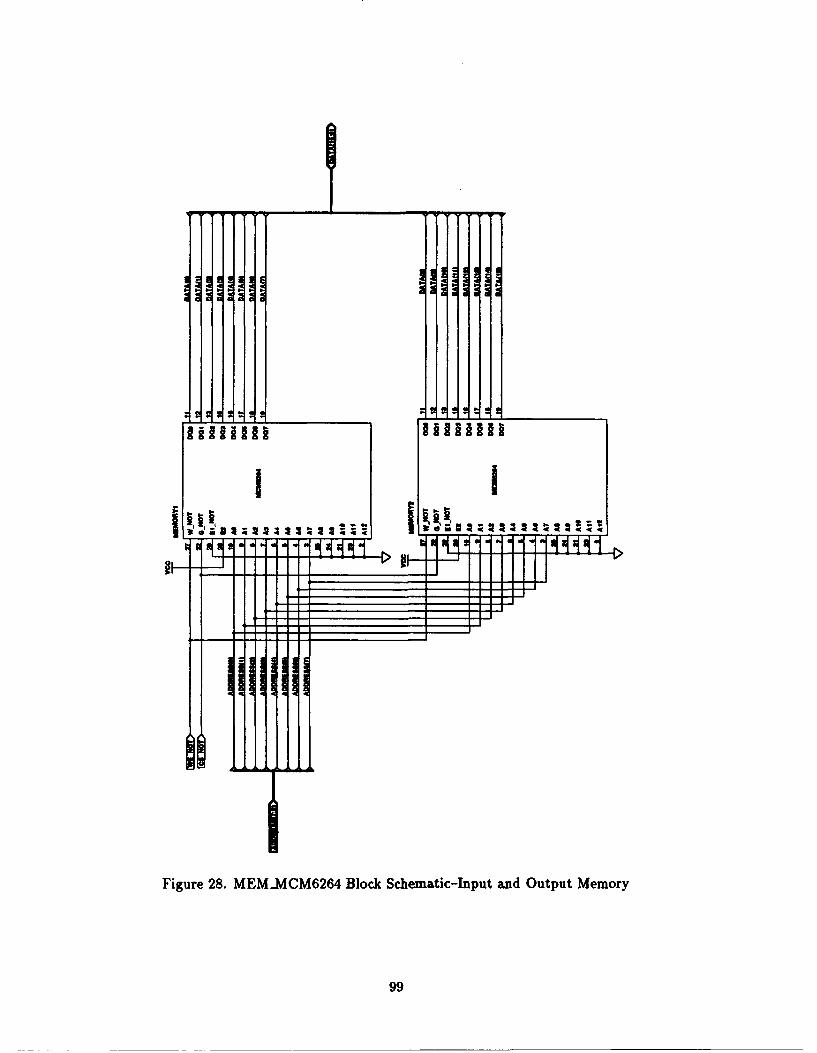
I
MiI II
i"Figure 28. MEM-MCM6264 Block Schematic-Input and Output Memory
99
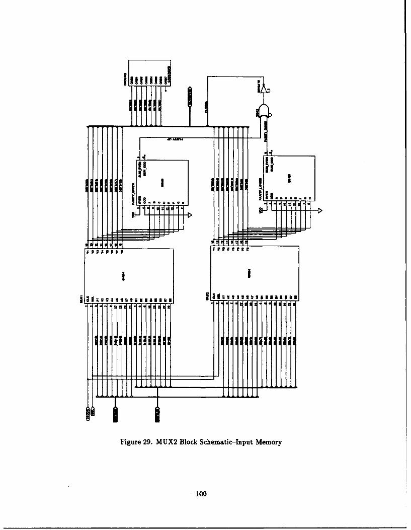
Figure 29. MUX2 Block Schematic-Input Memory
100
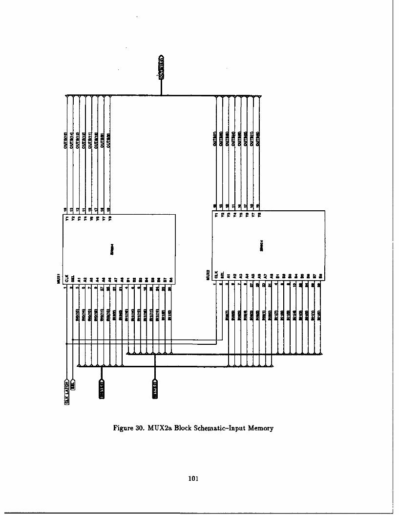
0a 0 a 0
I i
N C) 1ý
Figure 30. MUX2a Block Schematic-Input Memory
101
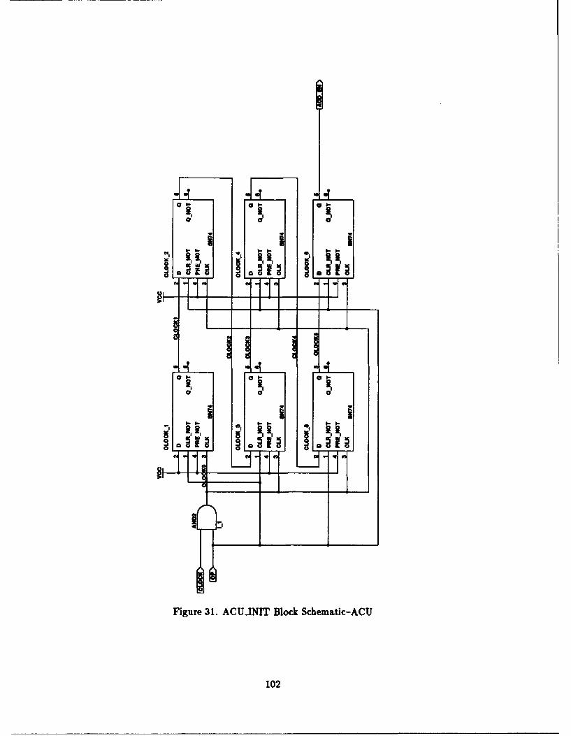
I I
Figur 31 jJI lc ceai-C
102 I
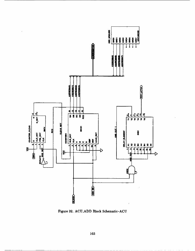
till,, ,,103
SIt
Figure 32. ACU.ADD Block Schematic-ACU
103
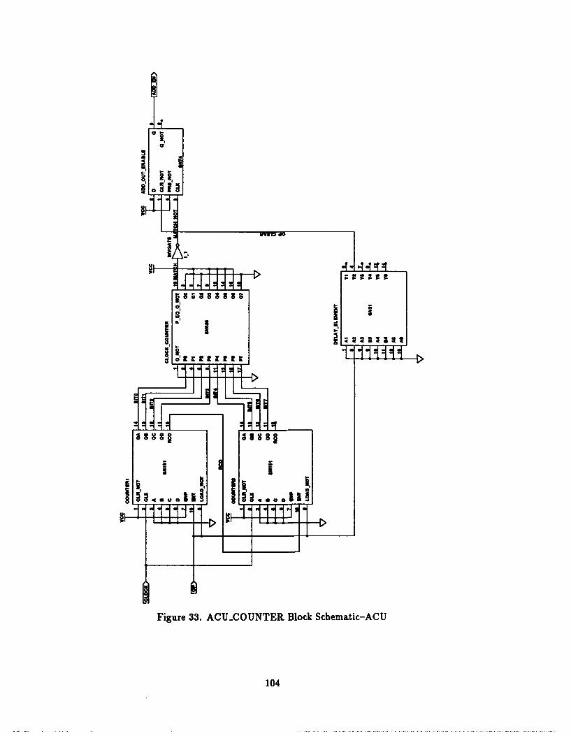
Figure 33. ACUCOUNTER Block SchematiclACU
104
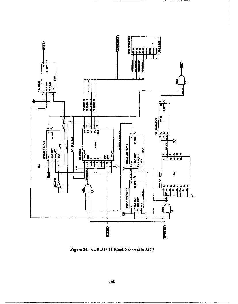
d I d
10
Ul l l l
° ! !I~
l'oJ~II!
F:1' _igur 34 CAD1BokSheai-
i105
Appendix B. Timing Diagrams for Functional Blocks
This appendix provides the timing diagrams generated for the major functional blocks
of the WFTA system which are discussed in Chapter IV. These timing diagrams show the
significant input and output signals of each block and each diagram is discussed in detail in
the text of the thesis. These timing diagrams were created from the test benchs discussed
in Section 4.5, using the trace option in the VHDL simulator provided with the Synopsys
software package. The behavior of the input signals was based on the expected signal
behavior from the WFTA system. All the values shown are in hexadecimal format.
106
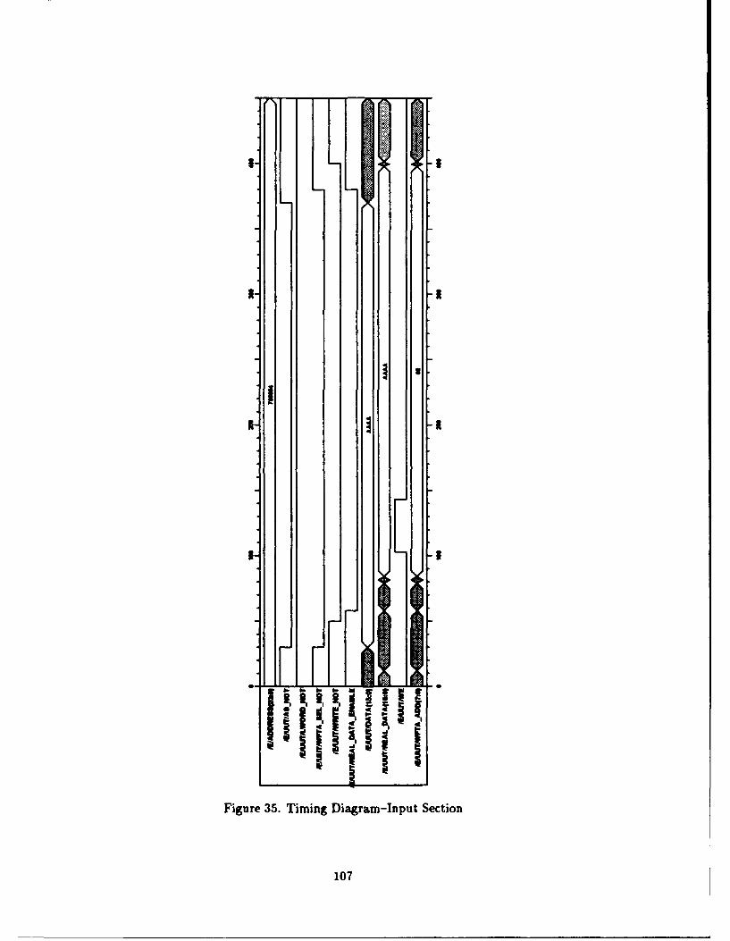
I L
Figure 35. Timing Diagram-Input Section
107
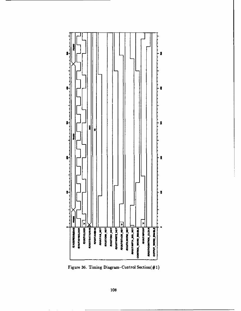
I I
I
I Im
I Uil
Figure 36. Timing Diagram-Control Section(# 1)
108
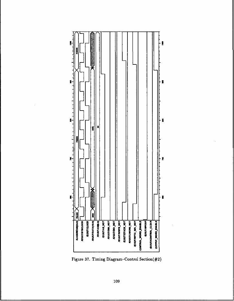
AL
3 3|
Im
I|
S|
o
II _j II
Figure 37. Timing Diagram-Control Section(#2)
109
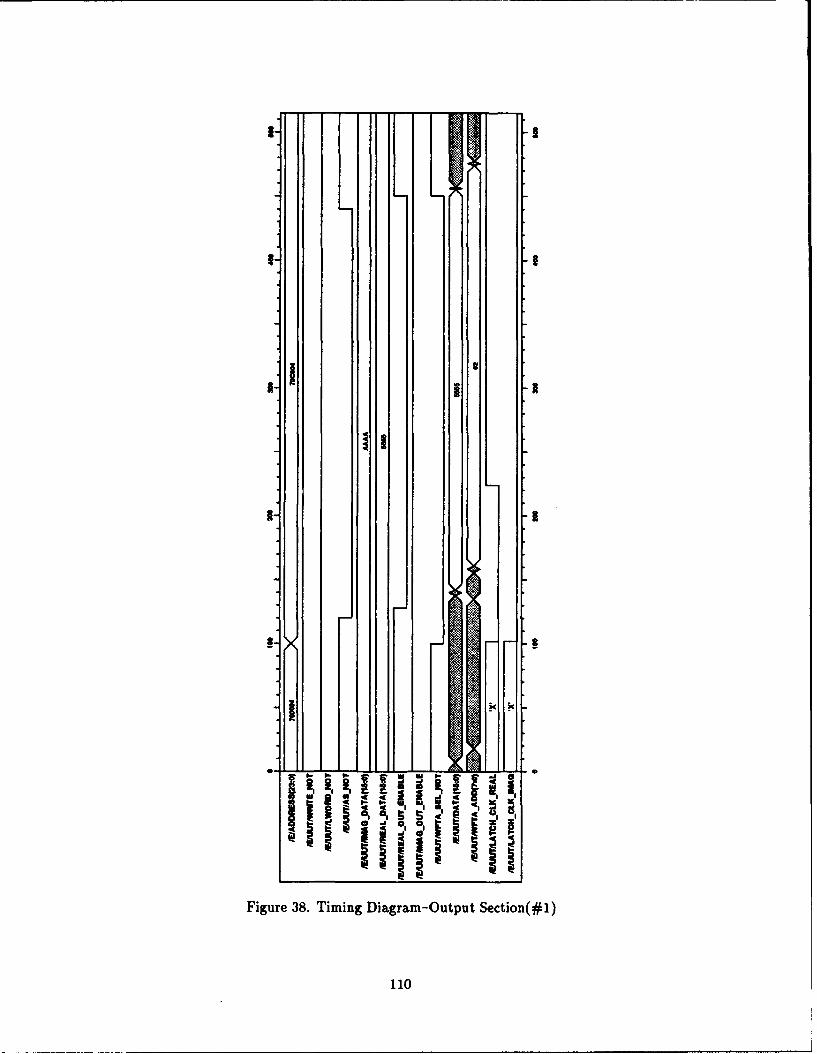
Ik k
i 3
11
I ' I ,ii iiI II I i, l 'II
Figure 38. Timing Diagram-Output Section(#1)
110
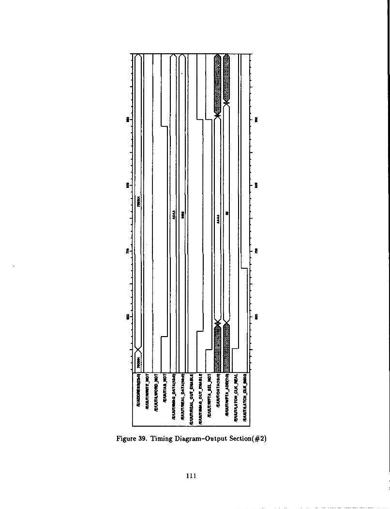
I i Il
Figr 3.TmnDiga - tutSc io( )
I111
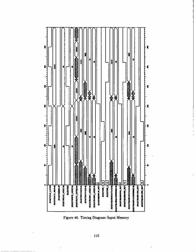
4 I1I
I IjFiue4.Tnln DarmIptMmr
I112
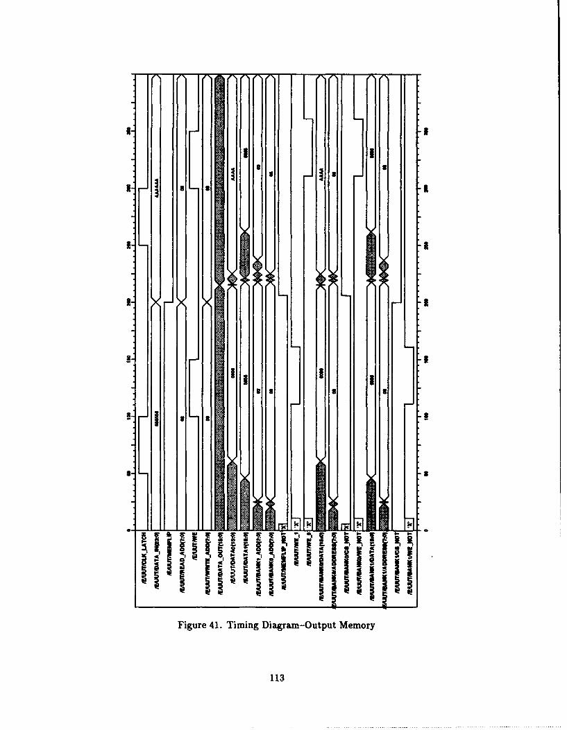
I i
II
- I
I I
..I Iii i ..* U
Figure 41. Timing Diagram-Output Memory
113
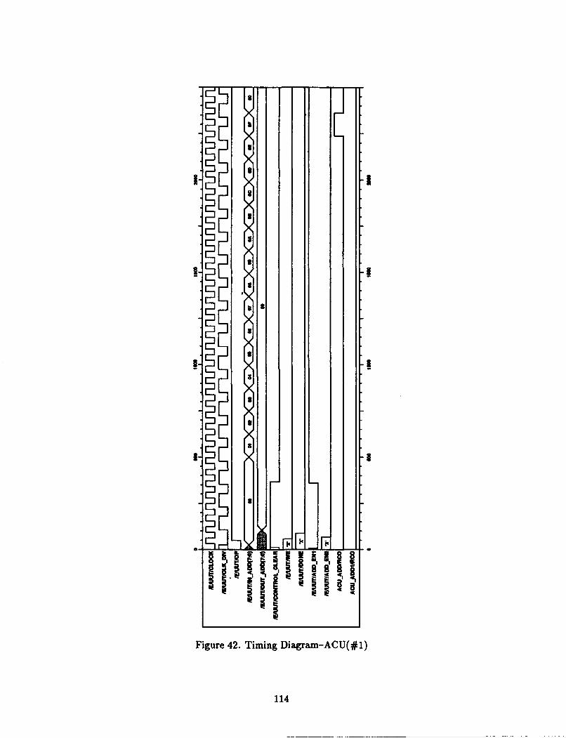
SE
3 1
3 Ii
I IUi ~ ~',
Uo
Figure 42. Timing Diagram-ACU(#l)
114
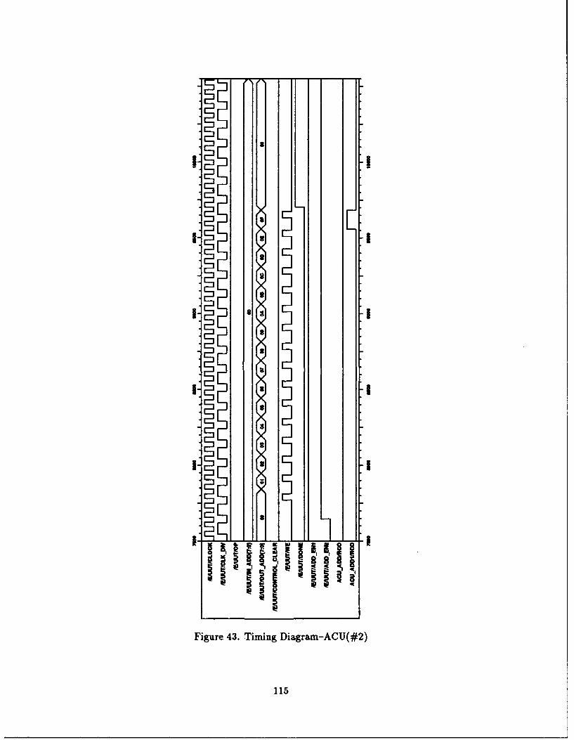
3
II
I I
Figure 4 3.TmnDirm-C(2
1115
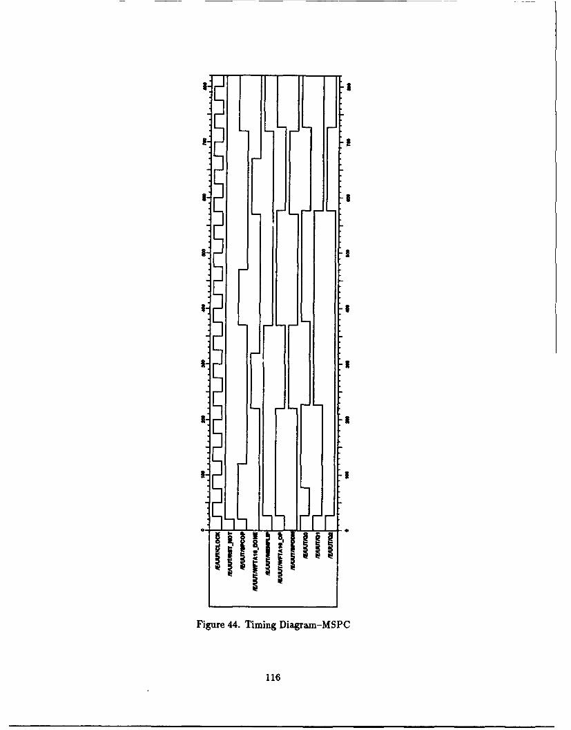
ai a
I I
I mI
a a
a a
III
Figure 44. Timing Diagram-MSPC
116
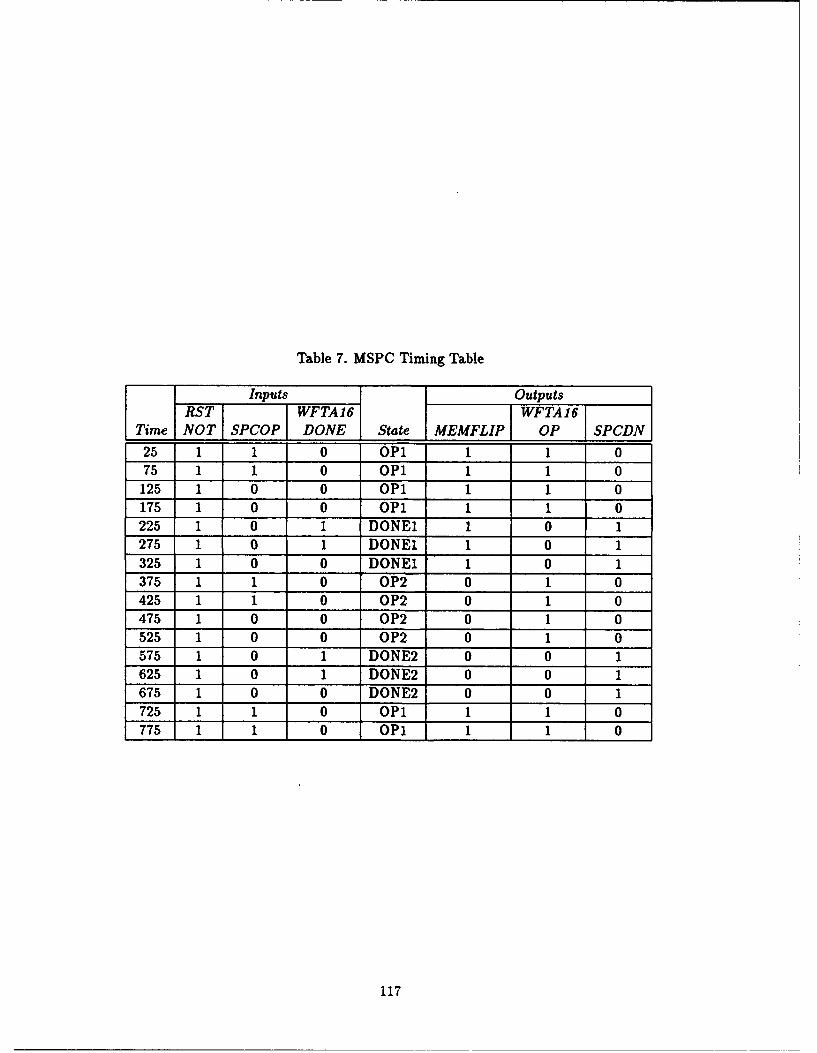
Table 7. MSPC Timing Table
Inputs OutputsRST WFTA16 WFTA16 SPCDN
Time NOT SPCOP DONE State MEMFLIP OP25 1 1 0 OPi 1 1 075 1 1 0 OPi 1 1 0125 1 0 0 OPi 1 1 0175 1 0 0 OPi 1 1 0225 1 0 1 DONE1 1 0 1275 1 0 1 DONE1 1 0 1325 1 0 0 DONE1 1 0 1375 1 1 0 OP2 0 1 0425 1 1 0 OP2 0 1 0475 1 0 0 OP2 0 1 0525 1 0 0 OP2 0 1 0575 1 0 1 DONE2 0 0 1625 1 0 1 DONE2 0 0 1675 1 0 0 DONE2 0 0 1725 1 1 0 OPi 1 1 0775 1 1 0 OPI 1 1 0
117
Appendix C. Test Vectors for 1 Hz Sine Wave
This appendix provides the test vectors used in verifying the WFTA system design
through the VHDL simulation. The signal used was a 1 Hz sine wave because both inputs
and outputs were known prior to simulation. All the test vectors have sixteen points of data
in a normalized 2's complement format. Table 8 shows the real input test vectors for a 1 Hz
sine wave. There are no imaginary input test vectors because the WFTA system designed
for this thesis does not accept imaginary input vectors. Table 9 shows the expected and
actual real output test vectors (or FFT) for a 1 Hz sine wave. Table 10 shows the expected
and actual imaginary output test vectors for a 1 Hz sine wave. The actual test vectors
were taken from the output file fourier-output after a simulation run.
118
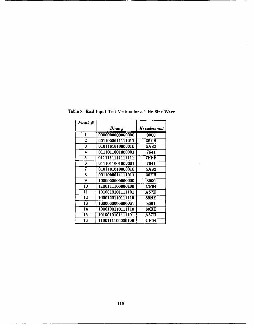
Table 8. Real Input Test Vectors for a 1 Hz Sine Wave
Point Binary Hexadecimal
1 0000000000000000 00002 0011000011111011 30FB3 0101101010000010 5A824 0111011001000001 76415 0111111111111111 7FFF6 0111011001000001 76417 0101101010000010 5A828 0011000011111011 30FB9 1000000000000000 800010 1100111100000100 CF0411 1010010101111101 A57D12 1000100110111110 89BE13 1000000000000001 800114 1000100110111110 89BE15 1010010101111101 A57D16 1100111100000100 CF04
119
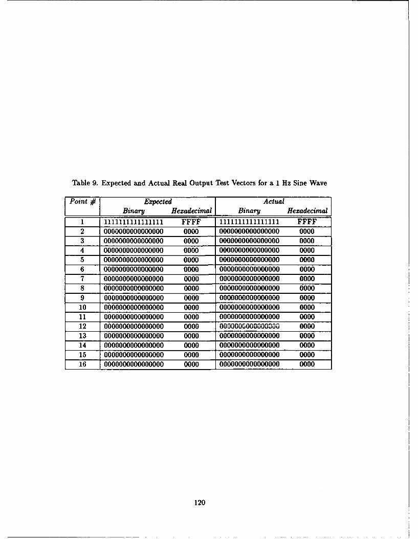
Table 9. Expected and Actual Real Output Test Vectors for a 1 Hz Sine Wave
Point # Expected ActualPoint Binary Hexadecimal Binary Hexadecimal
1 1111111111111111 FFFF 1111111111111111 FFFF
2 0000000000000000 0000 0000000000000000 00003 0000000000000000 0000 0000000000000000 00004 0000000000000000 0000 0000000000000000 00005 0000000000000000 0000 0000000000000000 00006 0000000000000000 0000 0000000000000000 00007 0000000000000000 0000 0000000000000000 00008 0000000000000000 0000 0000000000000000 00009 0000000000000000 0000 0000000000000000 000010 0000000000000000 0000 0000000000000000 000011 0000000000000000 0000 0000000000000000 000012 0000000000000000 0000 0000000000000030 000013 0000000000000000 0000 0000000000000000 000014 0000000000000000 0000 0000000000000000 000015 0000000000000000 0000 0000000000000000 000016 0000000000000000 0000 0000000000000000 0000
120
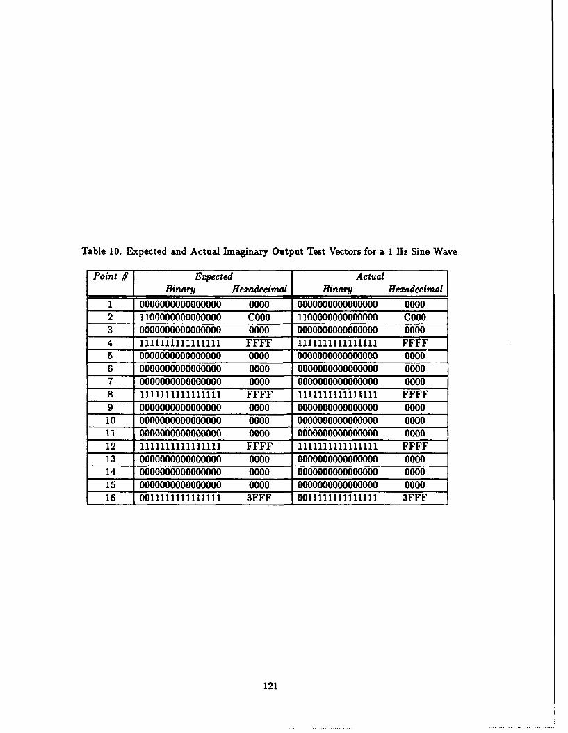
Table 10. Expected and Actual Imaginary Output Test Vectors for a 1 Hz Sine Wave
Point # Expected ActualBinary Hexadecimal Binary Hexadecimal
1 0000000000000000 0000 0000000000000000 00002 1100000000000000 C000 1100000000000000 C0003 0000000000000000 0000 0000000000000000 00004 1111111111111111 FFFF 1111111111111111 FFFF5 0000000000000000 0000 0000000000000000 00006 0000000000000000 0000 0000000000000000 00007 0000000000000000 0000 0000000000000000 00008 1111111111111111 FFFF 1111111111111111 FFFF9 0000000000000000 0000 0000000000000000 000010 0000000000000000 0000 0000000000000000 000011 0000000000000000 0000 0000000000000000 000012 1111111111111111 FFFF 1111111111111111 FFFF13 0000000000000000 0000 0000000000000000 000014 0000000000000000 0000 0000000000000000 000015 0000000000000000 0000 0000000000000000 000016 0011111111111111 3FFF 0011111111111111 3FFF
121
Appendix D. Timing Diagrams for WFTA System
This appendix provides the timing diagrams generated during the VHDL simulation
of the entire for the entire WFTA system. These timing diagrams were used in the veri-
fication of the system design in Chapter IV. All these timing diagrams are taken from a
single simulation using the input test vectors in Table 8. In order to better observe the
behavior of the signals the simulation was broken down into the seven timing diagrams
below, each one showing the signifcant actions of the WFTA system. All the values shown
are in hexadecimal format.
122
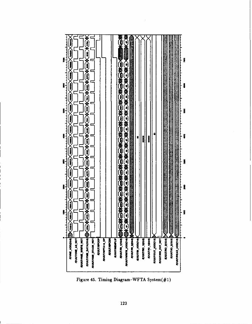
II
lIi
iiI iI i
I Il
Figure 45. Timing Diagram-WFTA Systemn(# 1)
123
ii IiIN
I I
Ii lI l i I
Figure 46. Timing Diagraxm-WFTA System(#2)
124
I-. a.
S[I Ii
I
SiRlIIII'I II
iIII I 11111Figure 47. Timing Diagralm-WFTA System(#3)
125
×I×N
it×R
1116
I I|
II
II
I - 1 11II
fill' 'j i ilIsIII
Figure 48. Timing Dia~gra~m-WFTA System(#4)
126
29U
olI
Figue 49 Tiing iagam-WTA yste(#I
12
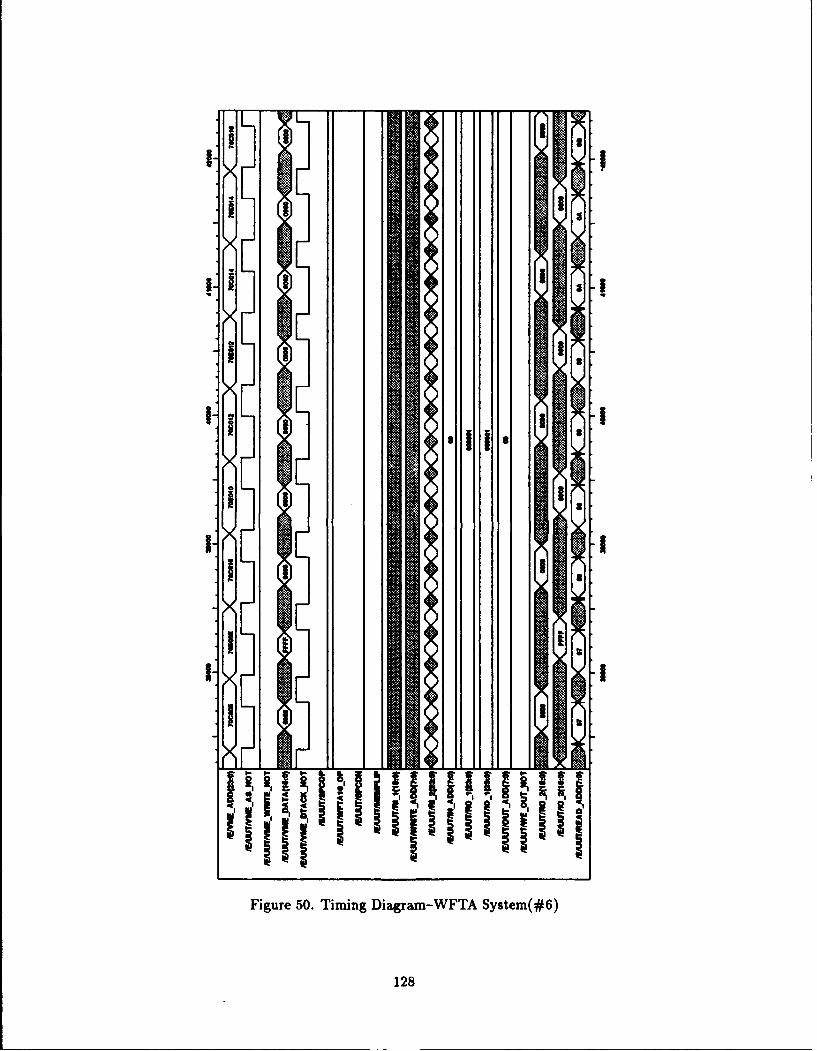
8
Figue5.TmngDa.mWTASse(
128~
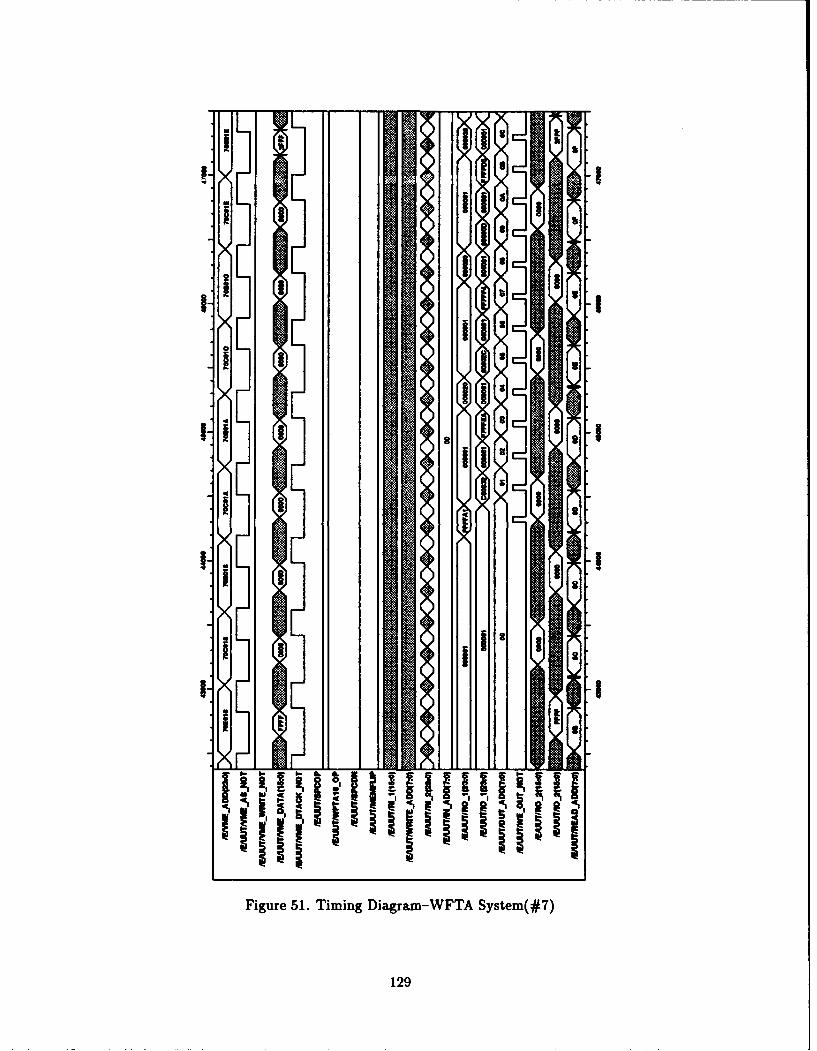
Figue 51 Tiing iagam-WTA yste(#7
129
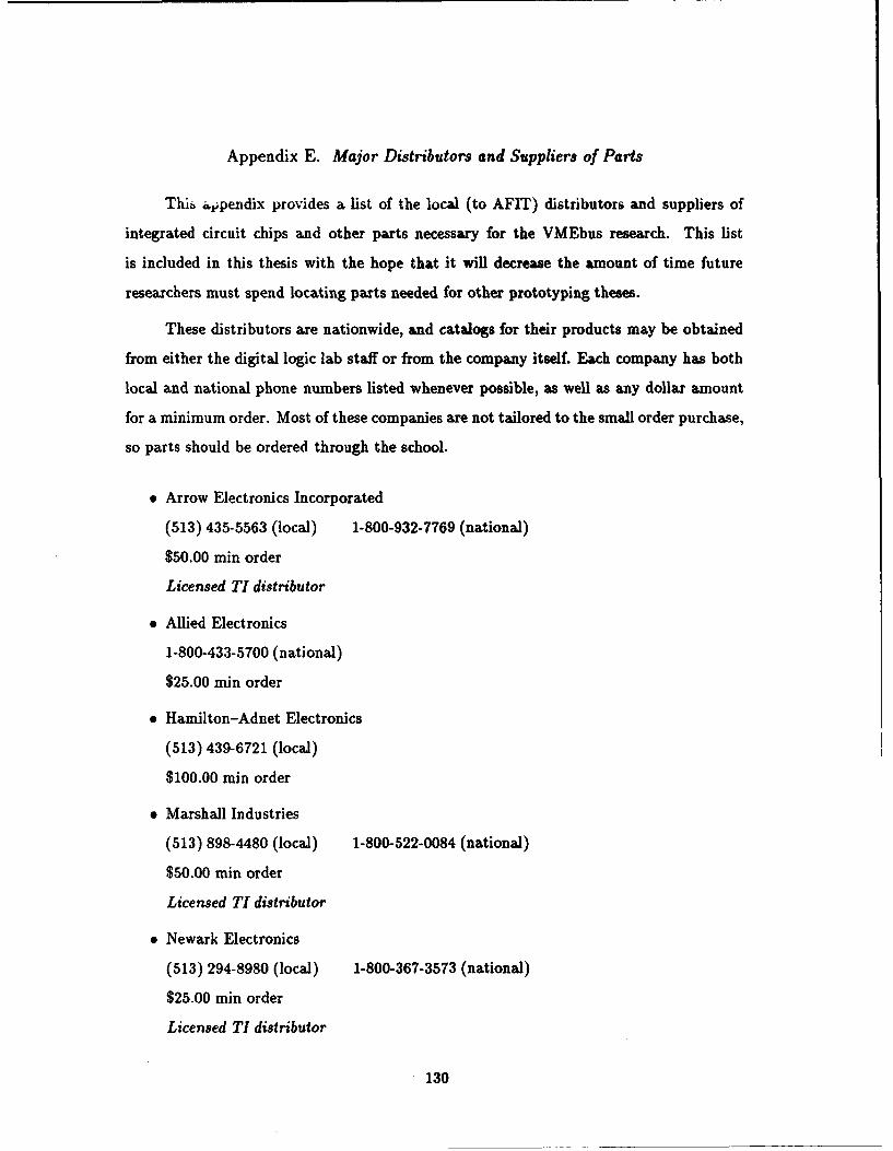
Appendix E. Major Distributors and Suppliers of Parts
This ,•ppendix provides a list of the local (to AFIT) distributors and suppliers of
integrated circuit chips and other parts necessary for the VMEbus research. This list
is included in this thesis with the hope that it will decrease the amount of time future
researchers must spend locating parts needed for other prototyping theses.
These distributors axe nationwide, and catalogs for their products may be obtained
from either the digital logic lab staff or from the company itself. Each company has both
local and national phone numbers listed whenever possible, as well as any dollar amount
for a minimum order. Most of these companies are not tailored to the small order purchase,
so parts should be ordered through the school.
"* Arrow Electronics Incorporated
(513) 435-5563 (local) 1-800-932-7769 (national)
$50.00 min order
Licensed TI distributor
"* Allied Electronics
1-800-433-5700 (national)
$25.00 min order
"* Hamilton-Adnet Electronics
(513) 439-6721 (local)
$100.00 min order
"* Marshall Industries
(513) 898-4480 (local) 1-800-522-0084 (national)
$50.00 min order
Licensed TI distributor
" Newark Electronics
(513) 294-8980 (local) 1-800-367-3573 (national)
$25.00 min order
Licensed TI distributor
130
One company that specializes in VMEbus boards and interconnects is the Vector
Electronic Company. The company might only operate through distributors, like the ones
above, but their address is included here to provide future researchers with a name of a
manufacturer of the products used in VMEbus design.
9 Vector Electronic Company
12460 Gladstone Avenue
Sylmar, California 91342
131
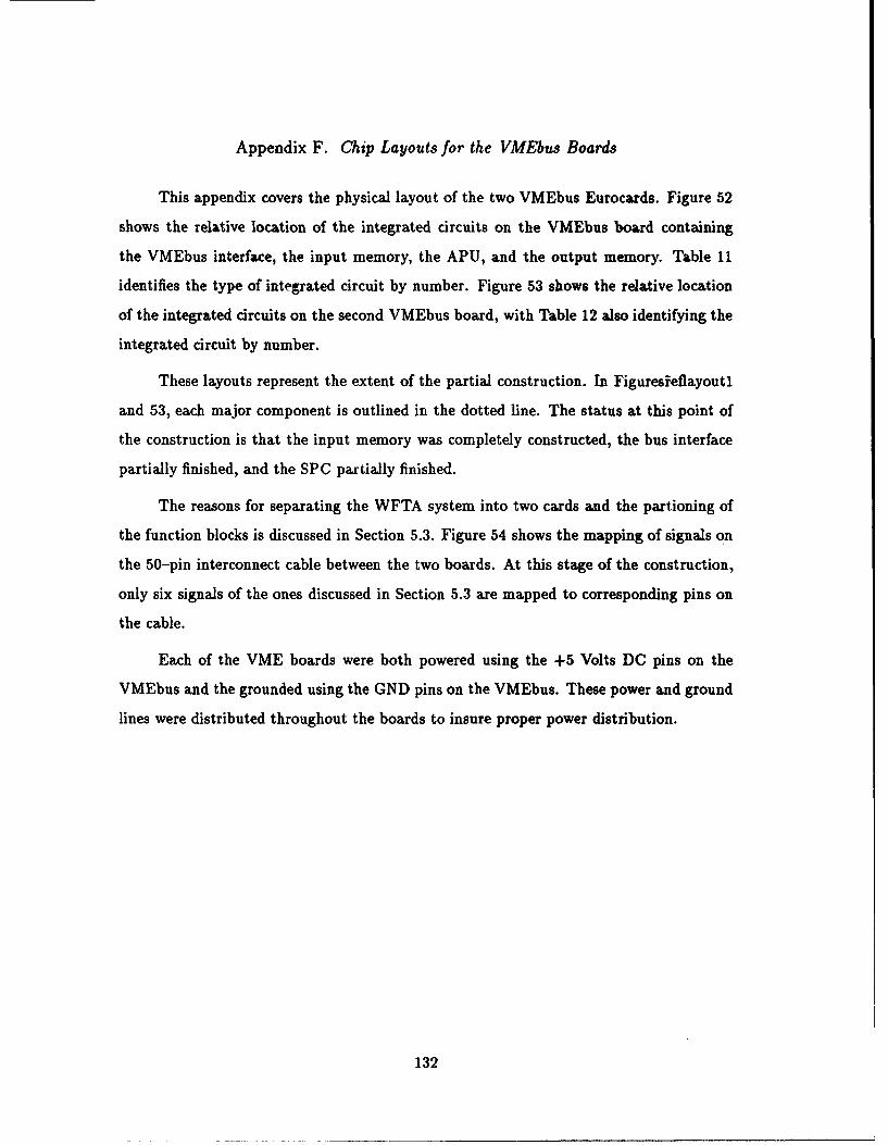
Appendix F. Chip Layouts for the VMEbus Boards
This appendix covers the physical layout of the two VMEbus Eurocards. Figure 52
shows the relative location of the integrated circuits on the VMEbus board containing
the VMEbus interface, the input memory, the APU, and the output memory. Table 11
identifies the type of integrated circuit by number. Figure 53 shows the relative location
of the integrated circuits on the second VMEbus board, with Table 12 also identifying the
integrated circuit by number.
These layouts represent the extent of the partial construction. In Figuresieflayoutl
and 53, each major component is outlined in the dotted line. The status at this point of
the construction is that the input memory was completely constructed, the bus interface
partially finished, and the SPC partially finished.
The reasons for separating the WFTA system into two cards and the partioning of
the function blocks is discussed in Section 5.3. Figure 54 shows the mapping of signals on
the 50-pin interconnect cable between the two boards. At this stage of the construction,
only six signals of the ones discussed in Section 5.3 are mapped to corresponding pins on
the cable.
Each of the VME boards were both powered using the +5 Volts DC pins on the
VMEbus and the grounded using the GND pins on the VMEbus. These power and ground
lines were distributed throughout the boards to insure proper power distribution.
132
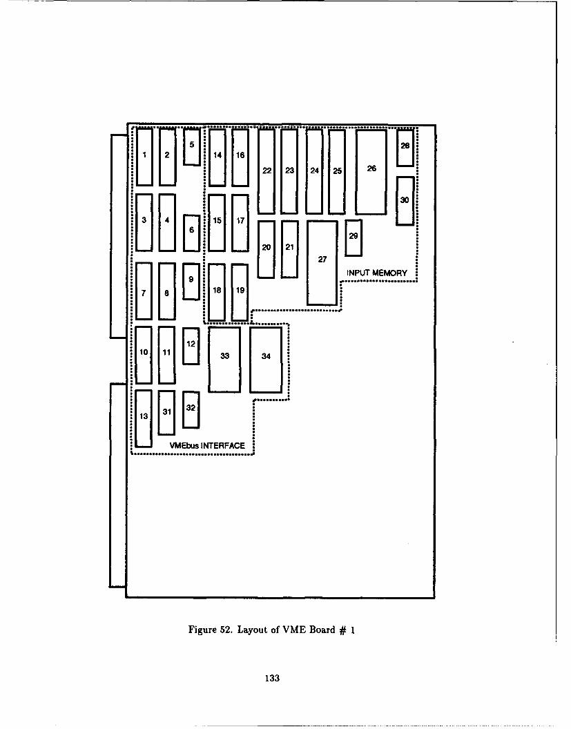
i n i28II 22 23 24 5i:FiO 24 25I 26 "irEy o VMS HQ27I
I-i NU MEMORY
..........
113
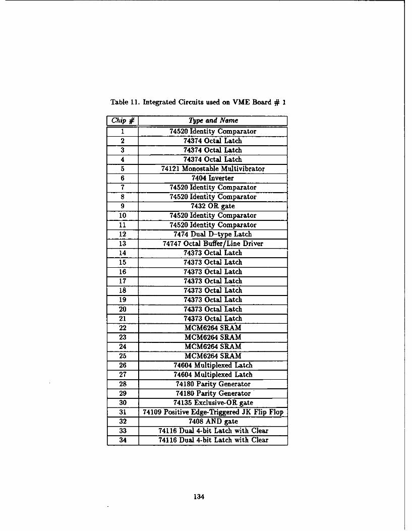
Table 11. Integrated Circuits used on VME Board # 1
Chip # Type and Name1 74520 Identity Comparator2 74374 Octal Latch3 74374 Octal Latch4 74374 Octal Latch5 74121 Monostable Multivibrator6 7404 Inverter7 74520 Identity Comparator8 74520 Identity Comparator9 7432 OR gate10 74520 Identity Comparator11 74520 Identity Comparator12 7474 Dual D-type Latch13 74747 Octal Buffer/Line Driver14 74373 Octal Latch15 74373 Octal Latch16 74373 Octal Latch17 74373 Octal Latch18 74373 Octal Latch19 74373 Octal Latch20 74373 Octal Latch21 74373 Octal Latch22 MCM6264 SRAM23 MCM6264 SRAM24 MCM6264 SIAM25 MCM6264 SRAM26 74604 Multiplexed Latch27 74604 Multiplexed Latch28 74180 Parity Generator29 74180 Parity Generator30 74135 Exclusive-OR gate31 74109 Positive Edge-Triggered JK Flip Flop32 7408 AND gate33 74116 Dual 4-bit Latch with Clear34 74116 Dual 4-bit Latch with Clear
134
Minimal SPC
Figure 53. Layout of VME Board # 2
135
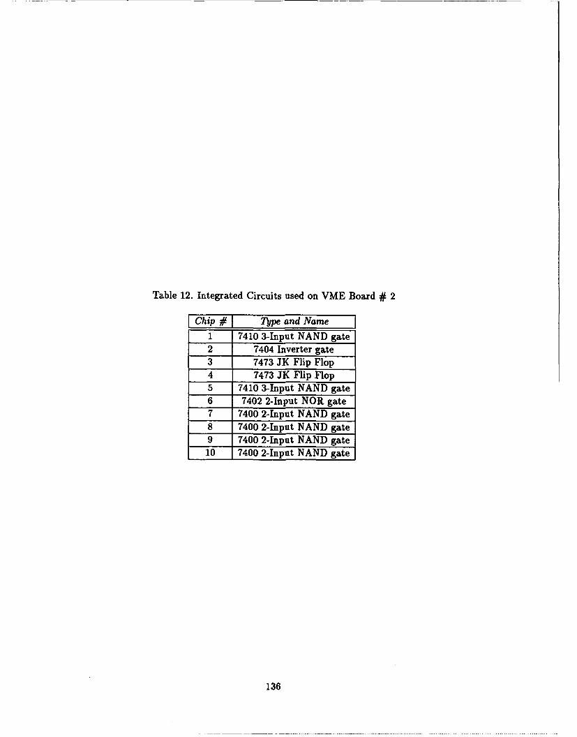
Table 12. Integrated Circuits used on VME Board # 2
Chip# Type and Name1 7410 3-Input NAND gate2 7404 Inverter gate3 7473 JIK Flip Flop4 7473 JIK Flip Flop5 7410 3-Input NAND gate6 7402 2-Input NOR gate7 7400 2-Input NAND gate8 7400 2-Input NAND gate9 7400 2-Input NAND gate10 7400 2-Input NAND gate
136
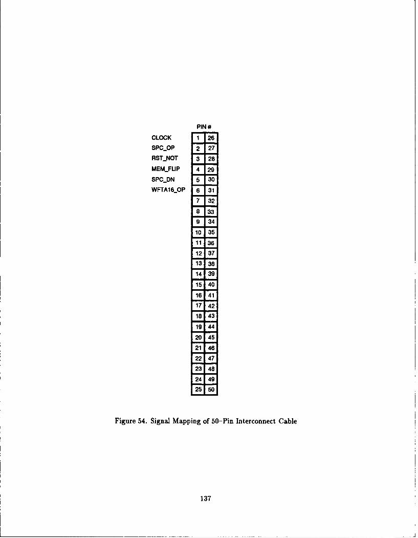
PIN #
CLOCK 1 26
SPCOP 2 27
RSTNOT 3 28
MEMFUP 4 29
SPCDN 5 30
WFTA16_OP 6 31
7 32
8 33
9 34
10 35
11 36
12 37
13 38
14 39
15 40
16 41
17 42
18 43
19 44
20 45
21 46
22 47
23 4824 49
25j 50
Figure 54. Signal Mapping of 50-Pin Interconnect Cable
137
Appendix G. Compilation, Download, and Run Procedures for Host Driver Code
This appendix describes the three procedures 1",veloped to compile, download, and
run procedures for the host driver code. These procedures are specific to the hardware
configuration used during this work. Different hardware setups would require modification
to these procedures. These procedures are documented since they are not intuitively
obvious and were developed because of system and resource constraints.
This appendix describes the general procedures for compiling, downloading, and
running the host driver program. The operator's manual of Appendix 3 gives the specific
commands, to include addresses, used for this thesis.
G.1 Compilation Procedure
The compiler used in this thesis was the Aztec C Compiler created by Manx Software
Systems. Its use is documented in the user's manual [38]. This compilation procedure
is covered in the text of the user's manual [38), but is confusing enough to make this
section necessary. The compiler software must be loaded onto a separate IBM-compatible
computer. The different steps are enumerated below with their associated commands.
1. Cr.tate the Source Program. Using any text editor, create the source code in C and
store it in a file.
2. Compile and Assemble. In order to compile and assemble the source code, use the
Aztec C Compiler command below.
c68 < filename >
This command will compile the C code in <filename> into assembly language and
then calls the assembler program contained in the Aztec C package in order to create
relocatable machine code.
138
3. Link. This relocatable machine code must be linked in order to associate it with a
particular arbitrary address in the system RAM. The use of this command is shown
below.
1n68 + d < address > -o < outputfilename > < filename >
The +d option tells the linker what to set the starting address of the program's
initialized data. The -o option tells the linker what name to call the output file.
Finally, the <filename> here is the name of the file which was compiled before.
4. Convert to Motorola S-records. This step converts the memory image generated by
the linker into Motorola S-records which will be used to load the RAM memory of
the host processor, a Motorola 68010 microprocessor. The command used for this
step is shown below.
srec68 < outputfilename >
The <output filename> here in.this command is the same that was used in the
linking step.
After compilation, machine code has been generated and is ready to be downloaded
into the system RAM of the host processor, along with the real input data points, which
is what the next section describes.
G.2 Download Procedure
Already mentioned in Chapter VI is the problem with I/O interface to the host
processor. This I/O limitation also precludes a different procedure to enter in the code
into the RAM of the host processor card. Using the debug monitor installed in the MVME-
120 card, only assembly level commands can be entered one line at a time, making the
entering of code tedious and prone to error. However, there is a means of overcoming this
obstacle.
139
After the host driver code has been compiled using the Aztec C Compiler, as described
in the compilation procedure discussed earlier, into machine language, the relocatable code
can then be linked, converted to S-records, and downloaded to the MVME-120 micropro-
cessor card using Kermit, a file transfer program. The VMEbus chassis has several RS-232
serial ports which can be used to download this compiled code. The one on the actual
microprocessor card (which is the default, port 1) is used to communicate to the dumb
terminal and cannot be used here. There are two ports in the back of the chassis which
can be used to transmit the data. Port number 2 specifies debug monitor port 2 which is
MVME-050 serial port 1 located in the back of the chassis and was used for this download
process.
The first step the downloading process is to configure the MVME-120 to receive the
data. The debug monitor command used is the Load S-records (LO) command. However,
before the use of this command, the port needs to set for the baud rate to be used for
transfering data. The default is 9600 baud, but it can be set to a slower speed. Setting the
data rate to a slower rate will insure the data will not be lost during downloading. The
command used for this is the Port Format (PF) command as shown below.
PF2
The number 2 in the command corresponds to the desired port used in the download
process. An interactive menu is presented, and the only option that needs to be changed
is the baud rate. When the debug monitor asks "Baud rate (1-5) = ....... $02 ?" the user
needs to answer 3 which corresponds to a baud rate of 2400 baud (which will have to be
set in the Kermit transfer program). A carriage return can be used to answer the rest of
the questions associated with the menu.
Once the baud rate has been set, the Load S-records command can be entered, at
which point the MVME-120 will wait for the data transfer. The command is shown below.
L02 ; X = DU <address>
140
The number 2 again corresponds to the port number that will be used for loading.
The ;x option is used to echo the S-records to the current debug port, or the screen in
this case. This option is used when the baud rate is slower than the default. The "= du
<address>" part of the command tells the debug monitor where in memory to store the
incoming data.
The next step in this procedure is to transmit the data through the RS-232 port
from the other computer using the Kermit file transfer program (although any file transfer
program can be used). This is a simple procedure, but the reader is cautioned to insure
that the data rate is set at the correct rate (2400 baud for this thesis) and the correct port
of the computer is set up for the data transfer.
Once completed, the Display Memory (MD) command can be used to verify that
data was actually transmitted to the desired location in the RAM. Although Motorola
S-records are not easily read and understood, the existence of data at that location in
memory is most likely an indication of a successful transfer.
The easiest way to load the raw data points is to use the Memory Modify (M or MM)
command and enter them one point at a time. The address used for this must correspond
to the one defined in the program. The command used for this was already discussed in
Section 5.4 of Chapter V with the only difference being that the ;N option does not need
to be used because the host processor can both read and write to the system RAM.
G.3 Run Procedure
After compiling and downloading the host driver code, and entering in the data for
an FFT, the program can now be run. The command used for executing the loaded host
driver program is the GO (G or GO) command and is shown below. The address used here
is the one where the transmitted data was loaded from in the downloading procedure.
GO <address>
141

Once the program has finished execution, the output data (real and imaginary) will
be written to some portion of the RAM of the host processor. In order to view the FFT
data, the Display Memory (MD) command can be used to examine the address where this
data was written.
142
Appendix H. Changes to Pseudocode for Sustained Operations
This appendix contains the necessary modifications to change the pseudocode of the
host driver program from single FFT operation to repeatable and sustained operations.
Figure 55 shows the additions. The additional loop is highlighted in capital letters and the
second write operation has been added. After the first write operation outside the loop
fills the pipeline for the first time, the entire process is repeated until there is no more
input data.
143
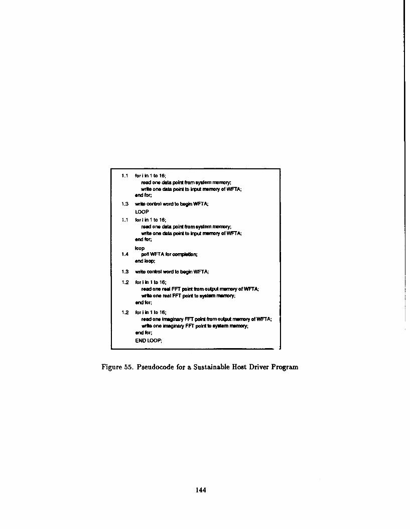
1.1 foriln 1to 16;road one data point from system memory,write one data point to input memory of WFTA;
end for;
1.3 write control word to begin WFT,4LOOP
1.1 forIin1to16;read one data point from system memory;write one data point to Input memory of WFTA;
end for;
loop1.4 poll WFTA for cormpltlon;
end loop,
1.3 write control word to begin WFTA;
1.2 for Iin 1to 16;read one real FFT point from outpt mernory of WFTA;write one real FFT point to system memory;
end for;
1.2 foriin 1 to 16;read one Imaginary FFT point from ouLptA memory of WFTA;write one imaginary FFT point to system memory;
end for;
END LOOP;
Figure 55. Pseudocode for a Sustainable Host Driver Program
144
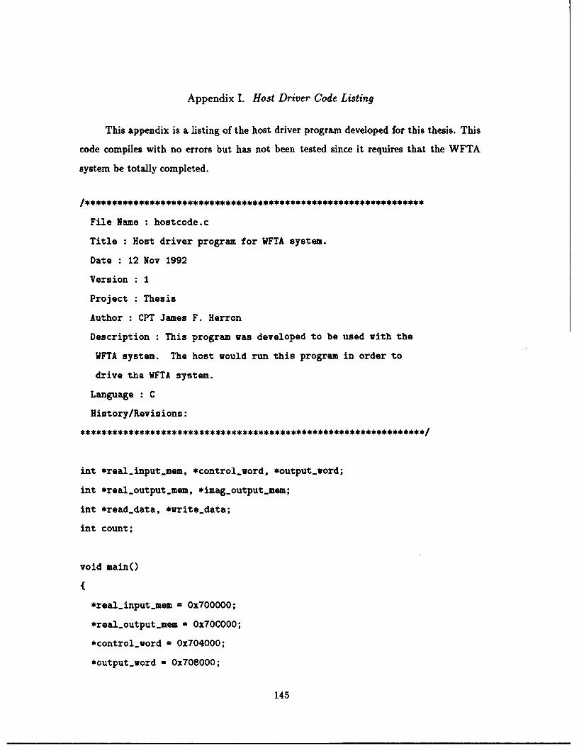
Appendix I. Host Driver Code Listing
This appendix is a listing of the host driver program developed for this thesis. This
code compiles with no errors but has not been tested since it requires that the WFTA
system be totally completed.
File Name : hostcode.c
Title Host driver program for WFTA system.
Date : 12 Nov 1992
Version : 1
Project : Thesis
Author : CPT James F. Herron
Description : This program was developed to be used with the
WFTA system. The host would run this program in order to
drive the WFTA system.
Language : C
History/Revisions:
int *real-input-mem, *control-word, *output.word;
int *real-output-mem, *imag.output.mem;
int *read-data, *write-data;
int count;
void main()
*real-input-mem = 0x700000;
*real-output-mem = OxTOCO0O;
*control-word i 0x704000;
*output.word = 0x708000;
145
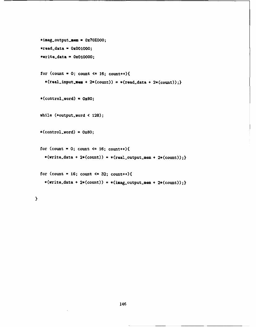
*imag...output-..u - Ox7OEOOO;
*read-data = OxOOlOOO;
*write-data = OxOlOOOO;
for (count a0; count <= 16; count+.){
*(real-input-mon~ + 2*(count)) = *(read-.data + 2*(count));}
* (control-word) a0x80;
while (*output..word < 128);
*(control-word) a0x80;
for (count = 0; count <= 16; count++){
*(write-.data + 2*(count)) = *(real..output..mem + 2*(count));}
for (count = 16; count <= 32; count++)(
*(write-.data + 2*(count)) = *(imag..output-.mem + 2*(count));}
146
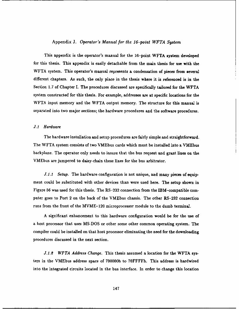
Appendix J. Operator's Manual for the 16-point WFTA System
This appendix is the operator's manual for the 16-point WFTA system developed
for this thesis. This appendix is easily detachable from the main thesis for use with the
WFTA system. This operator's manual represents a condensation of pieces from several
different chapters. As such, the only place in the thesis where it is referenced is in the
Section 1.7 of Chapter I. The procedures discussed are specifically tailored for the WFTA
system constructed for this thesis. For example, addresses are at specific locations for the
WFTA input memory and the WFTA output memory. The structure for this manual is
separated into two major sections; the hardware procedures and the software procedures.
J.1 Hardware
The hardware installation and setup procedures are fairly simple and straightforward.
The WFTA system consists of two VMEbus cards which must be installed into a VMEbus
backplane. The operator only needs to insure that the bus request and grant lines on the
VMEbus are jumpered to daisy-chain these lines for the bus arbitrator.
J.1. 1 Setup. The hardware configuration is not unique, and many pieces of equip-
ment could be substituted with other devices than were used here. The setup shown in
Figure 56 was used for this thesis. The RS-232 connection from the IBM-compatible com-
puter goes to Port 2 on the back of the VMEbus chassis. The other RS-232 connection
runs from the front of the MVME-120 microprocessor module to the dumb terminal.
A significant enhancement to this hardware configuration would be for the use of
a host processor that uses MS-DOS or other some other common operating system. The
compiler could be installed on that host processor eliminating the need for the downloading
procedures discussed in the next section.
J.1.2 WFTA Address Change. This thesis assumed a location for the WFTA sys-
tem in the VMEbus address space of 700000h to 70FFFFh. This address is hardwired
into the integrated circuits located in the bus interface. In order to change this location
147
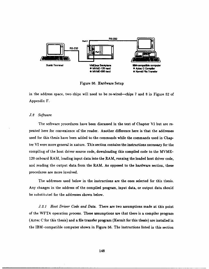
RS-23 2 R - a 0
Dumb Terninal VMEbue Baodln. lM-comnatblI conmpuerO MVME-120 ard 0 Aztec C Conmpier* MVME-050 card 0 Kerrnt Fil Transfer
Figure 56. Hardware Setup
in the address space, two chips will need to be re-wired--chips 7 and 8 in Figure 52 of
Appendix F.
J.2 Software
The software procedures have been discussed in the text of Chapter VI but are re-
peated here for convenience of the reader. Another difference here is that the addresses
used for this thesis have been added to the commands while the commands used in Chap-
ter VI were more general in nature. This section contains the instructions necessary for the
compiling of the host driver source code, downloading this compiled code to the MVME-
120 onboard RAM, loading input data into the RAM, running the loaded host driver code,
and reading the output data from the RAM. As opposed to the hardware section, these
procedures are more involved.
The addresses used below in the instructions are the ones selected for this thesis.
Any changes in the address of the compiled program, input data, or output data should
be substituted for the addresses shown below.
J.2.1 Host Driver Code and Data. There are two assumptions made at this point
of the WFTA operation process. These assumptions are that there is a compiler program
(Aztec C for this thesis) and a file transfer program (Kermit for this thesis) are installed in
the IBM-compatible computer shown in Figure 56. The instructions listed in this section
148
are for the application programs mentioned and should be modified for other software that
might be used.
J.2.1.1 Compiling the Host Driver Source Code. The compiler used in this
thesis was the Aztec C Compiler [38]. The different steps associated with the compilation
are enumerated below with their associated Aztec C commands. The procedure assumes
that the host driver code has previously been entered using a text editor and stored in a
file.
1. Compile and Assemble. In order to compile and assemble the source code, use the
Aztec C Compiler command that follows.
c68 < filename >
This command will compile the C code in <filename> into assembly language and
then calls the assembler program contained in the Aztec C software package in order
to create relocatable machine code.
2. Link. This relocatable machine code must then be linked in order to associate it
with a particular arbitrary address in the system RAM. The use of this command is
shown below.
1n68 + d 005000 - o < outputfilename > < filename >
The +d option tells the linker what to set the starting address (005000h in this
thesis) of the program's initialized data. The -o option tells the linker what name to
call the output file. Finally, the <filename> here is the name of the file which was
compiled before."
3. Convert to Motorola S-records. This step converts the memory image generated by
the linker into Motorola S-records which will be used to load the RAM memory of
the host processor, a Motorola 68010 microprocessor. The command used for this
step is shown below.
149
srec68 < outputfilename >
The <output filename> here in this command is the same that was used in the
linking step.
At this point, machine code has been generated and ready to be downloaded into the
RAM of the host processor along with the real input data points. The file that needs to
be downloaded is the one generated by the srec68 command.
J.2.1.2 Downloading the Compiled Host Driver Program. The first step of
the downloading process is to configure the MVME-120 microprocessor card to receive
the data. The MVME-120 uses a debug monitor, which consists of limited instruction set
defined in the read-only memory (ROM) of the MVME-120. The debug monitor command
used for this section is the Load S-records (LO) command. However, before the use of this
command, the port needs to set for the baud rate to be used for transfering data. The
default is 9600 baud, but it can be set to a slower speed. Setting the data rate to a slower
rate will insure the data will not be lost during downloading. The command used for this
is the Port Format (PF) command as shown below.
PF2
The number 2 in the command corresponds to the desired port used in the download
process. An interactive menu is presented, and the only option that needs to be changed
is the baud rate. When the debug monitor asks "Baud rate (1-5) = ....... $02 ?", answer
3, which corresponds to a baud rate of 2400 baud (which will have to also be set in the
Kermit transfer program). A carriage return can be used to answer the rest of the questions
associated with the menu.
Once the baud rate has been set, the Load S-records command can be entered, at
which point the MVME-120 will wait for the data transfer. The command is shown below.
150
L02 ;X = DU 005000
The number 2 again corresponds to the port number that will be used for loading.
The ;x option is used to echo the S-records to the current debug port, or the screen, in this
case. This option is used when the baud rate is slower than the default. Using this echo
option helps insure that the data transfer has actually occurred. The "= du 005000" part
of the command tells the debug monitor at what address in RAM to load the incoming
data.
The next step in this procedure is to transmit the data through the RS-232 port
from the other computer using the Kermit file transfer program (although any file transfer
programn can be used). This is a simple procedure, but be sure that the baud rate is set at
the correct rate (2400 baud for this thesis) and the correct port of the computer is set up
for the data transfer.
Once completed, the Display Memory (MD) debug monitor command can be used
to verify that data was actually transmitted to the desired location in the RAM. Although
Motorola S-records are not easily read and understood, the existence of data at that
location in memory is most likely an indication of a successful transfer.
J.2.1.3 Loading the Input Data. The easiest way to load the raw data points
is to use the debug monitor Memory Modify (M or MM) command and enter them one
point at a time. An example of the command follows. The address 001000h is the arbitary
location used in the host driver program to read the input data.
MM ; W 001000
The ;W option is used to write a 16-bit word. The operator enters in the data in
hexadecimal format until reaching 0010010h, at which time a lone carriage return exits the
memory modify command.
151
J.2.2 Running the Host Driver Program. The debug monitor command used for
executing the loaded host driver program is the GO (G or GO) command, shown below.
GO 005000
The address 005000h is the arbitrary location selected where the transmitted data
from the IBM-compatible computer was loaded in the downloading procedure.
J.2.3 Reading the Output Data. The debug monitor command used to read the
FFT data generated by the WFTA system is the Display Memory (MD) command and is
shown below.
MD 010000
The address 010000h is the arbitrary location that was used in the host driver pro-
gram to write the data that was read from the output memory of the WFTA system.
J.3 Problems in Operator's Manual
If the operator experiences any problems with the procedures in this appendix, ref-
erence the associated area of the thesis or consult troubleshooting procedures in the asso-
ciated manuals of the equipment or software.
152
Appendix K. VHDL Code and Schematic Listing
The size of this appendix makes it prohibitive to be included with the main thesis
and has been separated into a separate volume. This volume contains all the behavioral
and structural VHDL code for the WFTA prototype design discussed in this thesis. Also
included in this volume are the VHDL testbench code listing used to test the entities, as
well as sample output from these testbenches. Finally, this volume contains the Synopsys
generated schematics used in both the VHDL development and construction phase of this
thesis. This second volume will be stored in the VLSI laboratory.
153
References
1. C. Nuthalapati, "Role of High Speed FFT in Radar Signal Processing," MicrowaveJournal, pp. 163-180, October 1987.
2. K. W. Scribner, "Redesign, Simulation, and Development of a High-Speed,4080-Point Winograd Fast Fourier Transform Processor," Master's thesis,AFIT/GCE/ENG/91D-08, School of Engineering, Air Force Institute of Technology(AU), Wright-Patterson AFB OH, December 1991.
3. William H. Press et al., Numerical Receipes in C. Cambridge, Massachusetts: Cam-bridge University Press, 1988.
4. Mark T. Jong, Methods of Discrete Signal and System Analysis. New York, New York:McGraw-Hill Book Company, 1982.
5. William T. Cochran et al., "What is the Fast Fourier Transform?," in IEEE Transac-tions on Audio Electroacoustics, pp. 45-55, IEEE, 1967.
6. Schmuel Winograd, "On Computing the Discrete Fourier Transform," Mathematicsof Computation, pp. 175-199, January 1978.
7. Institute of Electrical and Electronic Engineers, IEEE Standard for a Versatile Bus:VMEbus, ANSI/IEEE Standard 1014-1987, (New York), IEEE, March 1987.
8. K. Taylor, "Architecture and Numerical Accuracy of High-Speed DFT ProcessingSystems," Master's thesis, AFIT/GE/ENG/85D-47, School of Engineering, Air ForceInstitute of Technology (AU), Wright-Patterson AFB OH, December 1985.
9. P. W. Coutee, "Arithmetic Cicuitry for High Speed VLSI Winograd Fourier Trans-form Processor," Master's thesis, AFIT/GE/ENG/85D-11, School of Engineering, AirForce Institute of Technology (AU), Wright-Patterson AFB OH, December 1985.
10. P. C. Rossbach, "Control Circuitry for High Speed VLSI Winograd Fourier Trans-form Processors," Master's thesis, AFIT/GE/ENG/85D-35, School of Engineering,Air Force Institute of Technology (AU), Wright-Patterson AFB OH, December 1985.
11. J. M. Collins, "Simulation and Modeling of a VLSI Winograd Fourier TransformAlgorithm," Master's thesis, AFIT/GE/ENG/85D-9, School of Engineering, Air ForceInstitute of Technology (AU), Wright-Patterson AFB OH, December 1985.
12. C. G. Shephard, "Integration and Design for Testability of a High Speed WinogradFourier Transform Processor," Master's thesis, AFIT/GE/ENG/86D-46, School ofEngineering, Air Force Institute of Technology (AU), Wright-Patterson AFB OH,December 1986.
13. G. D. Hedrick, "Design of Fault Tolerant Prime Factor Array Elements," Master'sthesis, AFIT/GE/ENG/86D-45,, Wright-Patterson AFB OH, December 1986.
14. C. H. Cooper, "Modeling and Simulation of the WFTA 16 Processor Using VHSICHardware Description Language," Master's thesis, AFIT/GE/ENG/86D-44, Schoolof Engineering, Air Force Institute of Technology (AU), Wright-Patterson AFB OH,December 1986.
154
15. R. S. Hauser, "Design Implemtation of a VLSI Prime Factor Algorithm Processor,"Master's thesis, AFIT/GCE/ENG/87D-5, School of Engineering, Air Force Instituteof Technology (AU), Wright-Patterson AFB OH, December 1987.
16. S. W. Pavick, "Testing and Data Path Redesign of a High Speed, 16-Point WinogradFourier Transform Processor," Master's thesis, AFIT/GE/ENG/89D-39, School ofEngineering, Air Force Institute of Technology (AU), Wright-Patterson AFB OH,December 1989.
17. R. R. Baker, "Modeling and Simulation of the Winograd Fourier Transform Pro-cessor," Master's thesis, AFIT/GE/ENG/90D-02, School of Engineering, Air ForceInstitute of Technology (AU), Wright-Patterson AFB OH, December 1990.
18. R. E. Sommer, "Microcell Library Development and 15-point Transform Chip De-sign for a High Speed WInograd Fourier Transform Processor," Master's thesis,AFIT/GE/ENG/90D-57, School of Engineering, Air Force Institute of Technology(AU), Wright-Patterson AFB OH, December 1990.
19. Robert M. Owens, Joseph Ja'Ja', "A VLSI Chip for the Winograd/Prime FactorAlgorithm to Compute the Discrete Fourier Transform," in IEEE Transactions onAcoustics, Speech, and Signal Processing, pp. 979-989, IEEE, 1986.
20. P. Lavoie, "A High-Speed CMOS Implementation of the Winograd Fourier TransformAlgorithm." Submitted to GOMAC, 1992.
21. M. Mehalic, Instructor. Personal interview. Air Force Institute of Technology, Wright-Patterson AFB OH, August 1992.
22. Roger Lipsett et al., VHDL: Hardware Description and Design. Boston, Mas-sachusetts: Kluwer Academic Publishers, 1989.
23. Institute of Electrical and Electronic Engineers, IEEE Standard VHDL Language Ref-
erence Manual, (New York), IEEE, 1987.
24. Synopsys, Inc., VHDL System Simulator Core Programs Manual, Version 2.2, Moun-tain View, CA, October 1991.
25. Synopsys, Inc., Simulation Graphical Environment User's Guide, Version 2.2, Moun-tain View, CA, October 1991.
26. Texas Instruments, The TTL Data Book Volume Two, Dallas, Texas, 1985.
27. Texas Instruments, ALS/AS Logic Data Book, Dallas, Texas, 1986.
28. Motorola Semiconductors, Memory Device Data, Austin, Texas, 1990.
29. Motorola Semiconductors, MC68010, 16-bit Virtual Memory Microprocessor, Austin,Texas, August 1983.
30. Synopsys, Inc., Design Compiler Reference Manual, Version 2.2, Mountain View, CA,October 1991.
31. C. P. Brothers, PhD candidate. Personal Interview. Air Force Institute of Technology,Wright-Patterson AFB OH, August 1992.
32. Motorola Semiconductors, MVME945 Chassis User's Manual, Phoenix, Arizona,February 1988.
155
33. Motorola Semiconductors, MVME12O, MVME121, MVME122, MVME123 VMEbusMicroprocessor Module User's Manual, Phoenix, Arizona, September 1984.
34. Hewlett Packard, Operating and Programming Manual Model 1631AID Logic Ana-lyzer, Colorado Springs, Colorado, August 1985.
35. Heath Company, Heathkit Manual for the Video Display Terminal Model H-29, BentonHarbor, Michigan, 1983.
36. Motorola Semiconductors, MVME12O Debug Monitor User's Manual, Phoenix, Ari-zona, Januaxy 1985.
37. R. S. Pressman, Software Engineering, A Practitioner's Approach. New York, NewYork: McGraw-Hill Publishing Company, 1987.
38. Manx Software Systems, Inc., Aztec C68k/ROM Cross Development System, Version3.4, Shrewsbury, New Jersey, November 1987.
156
Vita
CPT James F. Herron earned a Bachelor of Science in Electrical Engineering in
1986 at the United States Military Academy at West Point. Upon graduation he was
commissioned as a second lieutenant in the US Army Signal Corps. After attending the
Signal Officer's Basic Course and the Communications-Electronics Staff Officer Course,
he was assigned overseas and served with the 141st Signal Battalion, Ansbach, FRG and
34th Signal Battalion, Ludwigburg, FRG in a variety of positions. After returning from
overseas he then attended the Signal Officer's Advanced Course, the Echelon Above Corps
Course, and the Telecommunications Officer's Operations Course. In 1991 and 1992, CPT
Herron attended the Air Force Institute of Technology at Wright-Patterson AFB, where
he graduated with a Master of Science in Computer Engineering sequence specializing in
computer architecture and very large scale integrated circuit design.
Permanent address: 1849 S. BroadwayWichita, Kansas 67211
157
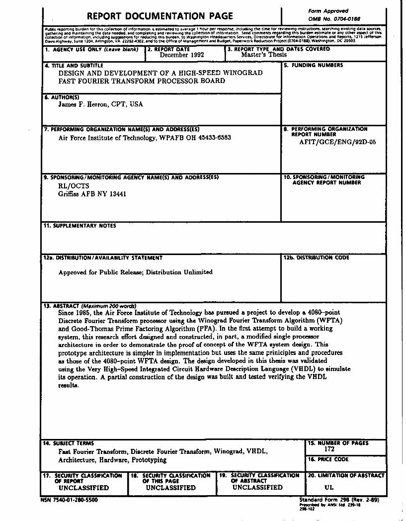
REPORT DOCUMENTATION PAGE Form Approved
Public reporting burden for this collection of information is estimated to average I hour per response, including the time for revi0Ming Bructions, searching existing data soN0rces8
gathering and maintaining the data needed, and completing and reviewing the collection of information. Send comments regoardng this burden estimate or any other aspect of thiscollection of information, including suggestions for reducing this burden, to Washington Headquarters Services, Directoate r information Operations and Reports, 1215 JeffersonDavis Highway, Suite 1204, Arlington. VA 22202-4302. and to the Office of Management and Budget. Paperwork Reduction Project (0704-0188), Washington, DC 20503.
1. AGENCY USE ONLY (Leave blank) 2. REPORT DATE 13. REPORT TYPE AND DATES COVERED
I December 1992 I Master's Thesis4. TITLE AND SUBTITLE 5. FUNDING NUMBERS
DESIGN AND DEVELOPMENT OF A HIGH-SPEED WINOGRADFAST FOURIER TRANSFORM PROCESSOR BOARD
6. AUTHOR(S)James F. Herron, CPT, USA
7. PERFORMING ORGANIZATION NAME(S) AND ADDRESS(ES) S. PERFORMING ORGANIZATION
Air Force Institute of Technology, WPAFB OH 45433-6583 REPORT NUMBERAFIT/GCE/ENG/92D-05
2. SPONSORING /MONITORING AGENCY NAME(S) AND ADDRESS(ES) 10. SPONSORING/ MONITORING
RL/OCTS AGENCY REPORT NUMBER
Griffiss AFB NY 13441
11. SUPPLEMENTARY NOTES
12a. DISTRIBUTION / AVAILABILITY STATEMENT 12b. DISTRIBUTION CODE
Approved for Public Release; Distribution Unlimited
13. ABSTRACT (Maximum 200 words)Since 1985, the Air Force Institute of Technology has pursued a project to develop a 4080-pointDiscrete Fourier Transform processor using the Winograd Fourier Transform Algorithm (WFTA)and Good-Thomas Prime Factoring Algorithm (PFA). In the first attempt to build a workingsystem, this research effort designed and constructed, in part, a modified single processorarchitecture in order to demonstrate the proof of concept of the WFTA system design. Thisprototype architecture is simpler in implementation but uses the same priniciples and proceduresas those of the 4080-point WFTA design. The design developed in this thesis was validatedusing the Very High-Speed Integrated Circuit Hardware Description Language (VHDL) to simulateits operation. A partial construction of the design was built and tested verifying the VHDLresults.
14. SUBJECT TERMS 15. NUMBER OF PAGES
Fast Fourier Transform, Discrete Fourier Transform, Winograd, VHDL, 172
Architecture, Hardware, Prototyping 16. PRICE CODE
17. SECURITY CLASSIFICATION IS. SECURITY CLASSIFICATION 19. SECURITY CLASSIFICATION 20. UMITATION OF ABSTRACTOF REPORT OF THIS PAGE OF ABSTRACT
UNCLASSIFIED UNCLASSIFIED UNCLASSIFIED UL
NSN 7540-01-280-5500 Standard Form 298 (Rev. 2-49)Prer by AN Std. M111112MI-02
GENERAL INSTRUCTIONS FOR COMPLETING SF 298
The Report Documentation Page (RDP) is used in announcing and cataloging reports. It is importantthat this information be consistent with the rest of the report, particularly the cover and title page.Instructions for filling in each block of the form follow. It is important to stay within the lines to meetoptical scanning requirements.
Block 1. Agency Use Only (Leave blank). Block 12a. Distribution/Availability Statement.Denotes public availability or limitations. Cite any
Block 2. Report Date. Full publication date availability to the public. Enter additionalincluding day, month, and year, if available (e.g. 1 limitations or special markings in all capitals (e.g.Jan 88). Must cite at least the year. NOFORN, REL, ITAR).
Block 3. Type of Report and Dates Covered. DOD - See DoDD 5230.24, DistributionState whether report is interim, final, etc. If S ee o n Technicalapplicable, enter inclusive report dates (e.g. 10 Statements on TechnicalJun 7-30Jun 8).Documents."Jun 87 - 30 Jun 88). DOE - See authorities.
Block 4. Title and Subtitle. A title is taken from NASA - See Handbook NHB 2200.2.the part of the report that provides the most NTIS - Leave blank.meaningful and complete information. When areport is prepared in more than one volume, Block 12b. Distribution Code.repeat the primary title, add volume number, andinclude subtitle for the specific volume. Onclassified documents enter the title classification DOD - Eave blank.in parentheses. DOE -Enter DOE distribution categories
from the Standard Distribution for
Block S. Fundinq Numbers. To include contract Unclassified Scientific and Technical
and grant numbers; may include program Reports.element number(s), project number(s), task NASA - Leave blank.
number(s), and work unit number(s). Use the NTIS - Leave blank.
following labels:
C - Contract PR - Project Block 13. Abstract. Include a brief (MaximumG - Grant TA - Task 200 words) factual summary of the mostPE - Program WU - Work Unit significant information contained in the report.
Element Accession No.
Block 6. Author(s). Name(s) of person(s) Block 14. Subiect Terms. Keywords or phrasesresponsible for writing the report, performing identifying major subjects in the report.the research, or credited with the content of thereport. If editor or compiler, this should followthe name(s). Block 15. Number of Pages. Enter the total
number of pages.Block 7. Performing Organization Name(s) andAddress(es). Self-explanatory. Block 16. Price Code. Enter appropriate price
Block 8. Performing Organization Report code (NTIS only).Number. Enter the unique alphanumeric reportnumber(s) assigned by the organization Blocks 17.- 19. Security Classifications. Self-performing the report. explanatory. Enter U.S. Security Classification in
Block 9. Sponsoring/Monitorincg Agency Name(s) accordance with U.S. Security Regulations (i.e.,and Address(es). Self-explanatory. UNCLASSIFIED). If form contains classified
information, stamp classification on the top andBlock 10. Sponsoring/Monitoring Aqency bottom of the page.Report Number. (If known)
Block 11. Supplementary Notes. Enter Block 20. Limitation of Abstract. This block mustinformation not included elsewhere such as: be completed to assign a limitation to thePrepared in cooperation with...; Trans. of...; To be abstract. Enter either UL (unlimited) or SAR (samepublished in.... When a report is revised, include as report). An entry in this block is necessary ifa statement whether the new report supersedes the abstract is to be limited. If blank, the abstractor supplements the older report. is assumed to be unlimited.
Standard Form 298 Back (Rev. 2-89)*U S GPO 190-0-273 271