Embed Size (px)
Citation preview
15
Thin Film Growth Through Sputtering Technique and Its Applications
Edgar Alfonso, Jairo Olaya and Gloria Cubillos Universidad Nacional de Colombia
Colombia
1. Introduction
During the last decade the dc and rf sputtering techniques have been used extensively in their two configurations — balanced and unbalanced magnetron. The main applications have been in the fields of industry and research. Examples of industrial applications are: decorative thin films (Raymond & Baham, 1999), hard wear-resistant thin films (Rodil & Olaya, 2006), low-friction thin films (Heimberg et al., 2001) corrosion-resistant thin films (Flores et al., 2006), and thin films used as a protective optical system (Stefan et al., 2008), as well as maybe the most interesting applications, thin films used in the electronic industry (Monroy et al., 2011). In the research field, the investigation has been oriented toward understanding the main physical mechanisms, such as: interaction between charged particles and the surface of the target material, adherence between the substrate and the deposited material, and chemical reactions near the substrate, as well as the influence of the deposit parameters (substrate temperature, working pressure, density power applied to the target). This research has produced thin films with a high degree of crystallinity and with the possibility of various industrial applications.
Moreover, researchers have made an effort to improve the system of operation. These efforts have been initiated through the so-called conventional or balanced magnetron sputtering in the early 1970s (Waits R, 1978), followed by the development of unbalanced systems in the late 1980s (Window, 1986) and its incorporation into multi-source “closed-field” systems in the early 1990s (Teer, 1989). Finally, the sputtering technique can increase the rate of deposition and ion energy by applying a unipolar high power pulse of low frequency and low duty cycle to the cathode target, referred to as high-power impulse magnetron sputtering (HiPIMS) or high-power pulsed magnetron sputtering (HPPMS). Common to all highly ionized techniques is very high density plasma. Implementing these discharges in sputter deposition technology modifies the surface of components, bringing improvements in mechanical, chemical, optical, electronic, and many other properties of the material. High-current glows are transient discharges operating at simultaneously high voltage (> 300 V) and high current density (> 100mAcm−2). They have recently proven successful for the deposition of thin-film materials. These developments have made it possible to have an exceptionally versatile technique, suitable for the deposition of high-quality, well-adhered films of a wide range of materials with high rates of deposition. Table 1 show the main applications obtained in the last decade with the magnetron sputtering (balanced and unbalanced) rf and dc versions.
Crystallization – Science and Technology
398
Technique Coating Reference
Balanced magnetron Nano-composites of NC-TiC wear applications
(Pavel, et al., 2011)
Balanced magnetron Optical properties of AlSiN nano-composites
(Liu, et al., 2009)
Balanced magnetron Hard coatings to decorative applications
(Raymond & Baham, 1999)
Balanced magnetron
Nd-Fe-B Film for magnetic applications
(Liu, et al., 20007)
Balanced magnetron Optical applications. (Stefan, et al., 2008)
Unbalanced magnetron Hard films for corrosion and wear applications
(Rodil & Olaya, 2006).
Unbalanced magnetron
Nb Films for biological applications
( Olivares, et al.,2011)
Unbalanced magnetron
NbO films for biological applications
( Ramirez, et al., 2011)
Unbalanced magnetron Electrical applications of NbN films.
( Olaya, et al., 2008,)
Unbalanced magnetron Diamond-like carbon films for infrared transmission enhancement
(Lingxia & Xu, 2000).
High power pulsed magnetron sputtering
Thin films for automotive engineering
(Bewilogua, et al., 2009)
High power pulsed magnetron sputtering
TiAlCN/VCN films for tribological applications
(Kamath, et al., 2011)
Table 1. Technological applications of thin films obtained with magnetron sputtering
In sputtering there are two means of operation: dc (diode and triode) and ac (radiofrequency), which also function in two configurations: magnetron dc (balanced and unbalanced) and magnetron ac (balanced and unbalanced).
In dc (diode) discharge, the cathode electrode is the sputtering target and the substrate is placed on the anode, which is often at ground potential (Vossen &Cuomo, 1978). The applied potential appears across a region very near the cathode, and the plasma generation region is near the cathode surface. The cathode in dc discharge must be an electrical conductor, since an insulating surface will develop a surface charge that will prevent ion bombardment of the surface. This condition implies that dc sputtering must be used to sputter simple electrically conductive materials such as metals, although the process is rather slow and expensive compared to vacuum deposition. An advantage of dc sputtering is that the plasma can be established uniformly over a large area, so that a solid large-area vaporization source can be established.
On the other hand, in dc sputtering the electrons that are ejected from the cathode are accelerated away from the cathode and are not efficiently used for sustaining the discharge. To avoid this effect, a magnetic field is added to the dc sputtering system that can deflect the electrons to near the target surface, and with appropriate arrangement of the magnets, the
Thin Film Growth Through Sputtering Technique and Its Applications
399
electrons can be made to circulate on a closed path on the target surface. This high current of electrons creates high-density plasma, from which ions can be extracted to sputter the target material, producing a magnetron sputter configuration (Penfold, 1995). A disadvantage of the magnetron sputtering configuration is that the plasma is confined near the cathode and is not available to active reactive gases in the plasma near the substrate for reactive sputter deposition. This difficulty can be overcome using an unbalanced magnetron configuration (see Fig. 1), where the magnetic field is such that some electrons can escape from the cathode region (Windows & Savvides, 1986). A disadvantage of the unbalanced magnetron is that the current of escaping electrons is not uniform, and the plasma generated is not uniform.
In ac sputtering, working at frequencies below about 50 kHz, the potential on the target is periodically reversed, and the ions have enough mobility so that a dc diode-like discharge, where the total potential drop is near the cathode, can be formed alternately on each electrode. The substrate chamber walls can be used as the counterelectrode. At frequencies above 50 kHz, the ions do not have enough mobility to allow establishing a dc-diode-like discharge and the applied potential is felt throughout the space between electrodes. The electrons acquire sufficient energy to cause ionizing collisions in the space between the electrodes. When an rf potential with a large peak-to-peak voltage is capacitively coupled to an electrode, an alternating positive-negative potential appears on the surface. During part of each half-cycle, the potential is such that ions are accelerated to the surface with enough energy to cause sputtering, while in alternate half-cycles, electrons reach the surface and prevent any charge buildup. Rf sputtering can be used to sputter insulating material, although the sputtering rate is low. A major disadvantage of rf sputtering of dielectric targets is that most insulating materials have poor thermal conductivity and high coefficients of thermal expansion, and are usually brittle materials. Since most of the bombarding energy produces heat, this means that large thermal gradients can be generated that result in fracturing the target if high power levels are used.
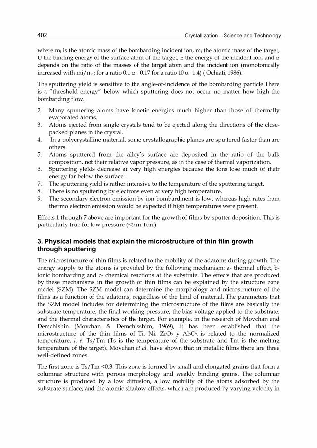
Fig. 1. Schematic configuration of the a- balanced magnetron (intermediate) and b- unbalanced magnetron (type 1and type 2 ( B. Window & N. Savvides, 1986)
Crystallization – Science and Technology
400
Rf sputtering can be used with a magnetic field in balanced and unbalanced configurations to obtain a result similar to dc-like diode discharge. In fig 2 the different configurations of dc and rf sputtering are shown.
a)
b)
Fig. 2. Sputtering configurations a) dc sputtering, b) rf sputtering
It is important to state that in all the cases discussed above, the target and the substrate were facing (on- axis sputtering). In this configuration, the highly energetic electrons irradiate the substrates and/or the growing surface of the thin films during deposition. Off-axis sputtering reduces the effects of the irradiation of the high-energy particles. In off-axis sputtering, the substrates are settled at the outside of the discharge plasma. The thickness distribution of thin films deposited by off-axis sputtering will be larger than that for on-axis sputtering. A rotating substrate holder with a metal shadow mask is used for the reduction of the thickness distribution of the off-axis sputtering. Under a suitable design, the thickness distribution is less than 2% for substrates of 100 × 100 mm in an rf sputtering system using a 5-inch target (Shibahara et al., 1987).
Thin Film Growth Through Sputtering Technique and Its Applications
401
In this chapter we will present the physical parameters involved in the growth of thin films; also discussed will be the influence that the growth parameters have on the degree crystallinity of the films, the chemical characterization, and the optical characterization of the films; and finally, we will discuss the residual stress, hardness, and corrosion and wear resistance of thin films.
2. Physical sputtering
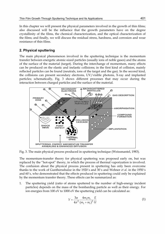
The main physical phenomenon involved in the sputtering technique is the momentum transfer between energetic atomic-sized particles (usually ions of noble gases) and the atoms of the surface of the material (target). During the interchange of momentum, many effects can be produced on the elastic and inelastic collisions; in the first kind of collision, mainly reflected particles can be found (neutrals, ions of the target and the gas). In the second kind, the collisions can present secondary electrons, UV/visible photons, X-ray and implanted particles; schematically, Fig. 3 shows different processes that may occur during the interaction between charged particles and the surface of the material.
Fig. 3. The main physical process produced in sputtering technique (Weissmantel, 1983).
The momentum-transfer theory for physical sputtering was proposed early on, but was replaced by the “hot-spot” theory, in which the process of thermal vaporization is involved. The confusion about the physical process present in sputtering has only been overcome thanks to the work of Gunthersshulze in the 1920´s and 30´s and Wehner et al. in the 1950´s and 60´s, who demonstrated that the effects produced in sputtering could only be explained by the momentum transfer theory. These effects can be summarized as:
1. The sputtering yield (ratio of atoms sputtered to the number of high-energy incident particles) depends on the mass of the bombarding particle as well as their energy. For ion energies from 100 eV to 1000 eV the sputtering yield can be calculated as:
12 2
1
434 ( )
t
t
m m EY
Um m
(1)
Crystallization – Science and Technology
402
where mi is the atomic mass of the bombarding incident ion, mt the atomic mass of the target, U the binding energy of the surface atom of the target, E the energy of the incident ion, and depends on the ratio of the masses of the target atom and the incident ion (monotonically increased with mi/mt ; for a ratio 0.1 = 0.17 for a ratio 10 =1.4) ( Ochiati, 1986).
The sputtering yield is sensitive to the angle-of-incidence of the bombarding particle.There is a “threshold energy” below which sputtering does not occur no matter how high the bombarding flow.
2. Many sputtering atoms have kinetic energies much higher than those of thermally evaporated atoms.
3. Atoms ejected from single crystals tend to be ejected along the directions of the close-packed planes in the crystal.
4. In a polycrystalline material, some crystallographic planes are sputtered faster than are others.
5. Atoms sputtered from the alloy’s surface are deposited in the ratio of the bulk composition, not their relative vapor pressure, as in the case of thermal vaporization.
6. Sputtering yields decrease at very high energies because the ions lose much of their energy far below the surface.
7. The sputtering yield is rather intensive to the temperature of the sputtering target. 8. There is no sputtering by electrons even at very high temperature. 9. The secondary electron emission by ion bombardment is low, whereas high rates from
thermo electron emission would be expected if high temperatures were present.
Effects 1 through 7 above are important for the growth of films by sputter deposition. This is particularly true for low pressure (<5 m Torr).
3. Physical models that explain the microstructure of thin film growth through sputtering
The microstructure of thin films is related to the mobility of the adatoms during growth. The energy supply to the atoms is provided by the following mechanism: a- thermal effect, b- ionic bombarding and c- chemical reactions at the substrate. The effects that are produced by these mechanisms in the growth of thin films can be explained by the structure zone model (SZM). The SZM model can determine the morphology and microstructure of the films as a function of the adatoms, regardless of the kind of material. The parameters that the SZM model includes for determining the microstructure of the films are basically the substrate temperature, the final working pressure, the bias voltage applied to the substrate, and the thermal characteristics of the target. For example, in the research of Movchan and Demchishin (Movchan & Demchisshim, 1969), it has been established that the microstructure of the thin films of Ti, Ni, ZrO2 y Al2O3 is related to the normalized temperature, i. e. Ts/Tm (Ts is the temperature of the substrate and Tm is the melting temperature of the target). Movchan et al. have shown that in metallic films there are three well-defined zones.
The first zone is Ts/Tm <0.3. This zone is formed by small and elongated grains that form a columnar structure with porous morphology and weakly binding grains. The columnar structure is produced by a low diffusion, a low mobility of the atoms adsorbed by the substrate surface, and the atomic shadow effects, which are produced by varying velocity in
Thin Film Growth Through Sputtering Technique and Its Applications
403
the growth the columns and the various incidence angles at which the atoms arrive at the surface of the substrate. In the second zone, 0.3≤ Ts/Tm≤0.45, the substrate temperature increasing homogeneous which leads to a higher diffusion of the adatoms, which produce a dense structure with a higher degree of binding among the columns and the borders between columns, with borders of the grain beginning to form. In this zone, the size of the grain can be increased and the grains extended in equiaxed form, from interface substrate-film to film surface. In the third zone, Ts/Tm>0.45, the volumetric diffusion size has a great influence on the morphology of the film, due to the increase in the diffusion into the grains, which produces growth of the grains, formation of the equiaxed grain and re-crystallization. These effects produce a greater crystalline structure.
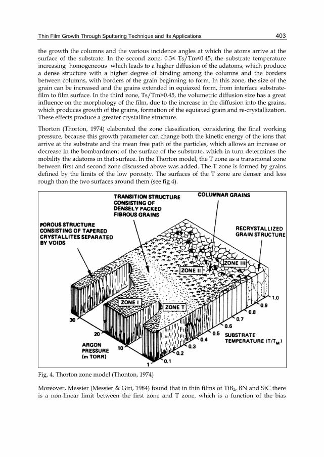
Thorton (Thorton, 1974) elaborated the zone classification, considering the final working pressure, because this growth parameter can change both the kinetic energy of the ions that arrive at the substrate and the mean free path of the particles, which allows an increase or decrease in the bombardment of the surface of the substrate, which in turn determines the mobility the adatoms in that surface. In the Thorton model, the T zone as a transitional zone between first and second zone discussed above was added. The T zone is formed by grains defined by the limits of the low porosity. The surfaces of the T zone are denser and less rough than the two surfaces around them (see fig 4).
Fig. 4. Thorton zone model (Thonton, 1974)
Moreover, Messier (Messier & Giri, 1984) found that in thin films of TiB2, BN and SiC there is a non-linear limit between the first zone and T zone, which is a function of the bias
Crystallization – Science and Technology
404
voltage applied to the substrate. The bias voltage of the substrate has the same effect on the mobility and adsorption of the atoms as an increase in the temperature, so when it is increased, the T zone increases and the first zone decreases, resulting in denser thin films and with a high degree of crystallinity.
The bias voltage also influences the mechanical properties of thin films; for example, with a voltage (≥100V) applied to the substrate, the deformation of the lattice increases, causing high residual efforts and low adherence between the substrate and the film.
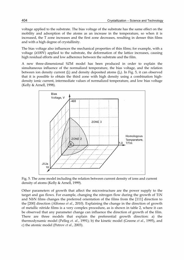
A new three-dimensional SZM model has been produced in order to explain the simultaneous influence of the normalized temperature, the bias voltage, and the relation between ion density current (Ji) and density deposited atoms (Ja). In Fig. 5, it can observed that it is possible to obtain the third zone with high density using a combination high-density ionic current, intermediate values of normalized temperature, and low bias voltage (Kelly & Arnell, 1998).
Fig. 5. The zone model including the relation between current density of ions and current density of atoms (Kelly & Arnell, 1999).
Other parameters of growth that affect the microstructure are the power supply to the target and gas flows. For example, changing the nitrogen flow during the growth of TiN and NbN films changes the preferred orientation of the films from the [111] direction to the [200] direction (Alfonso et al., 2010). Explaining the change in the direction of growth of metallic nitride films is a very complex procedure, as is shown in table 2, where it can be observed that any parameter change can influence the direction of growth of the film. There are three models that explain the preferential growth direction: a) the thermodynamic model (Pelleg et. al., 1991); b) the kinetic model (Greene et al., 1995), and c) the atomic model (Petrov et al., 2003).

Thin Film Growth Through Sputtering Technique and Its Applications
405
Material Parameter Change of orientation References TiN Ji/Ja (111) → (200) (Green et al., 1995)
N2/Ar (111) → (200) (Noda et al., 2002) Th Mixed → (200) → (111) (Pelleg et al., 1991) Vb (200) → (111) → (220) (Kobayashi & Doy,
1984) W (200) → (111) (Je et al., 1997). T (111) → (200) (Cheng et al., 2002)
AlN P axis c → axis a (Lee & Y. Lee, 1994) ds-t axis c → axis a (Ishihara et al., 1998) λ/ds-t axis a → axis c (Ishihara et al., 1998)
N2/Ar axis a → axis c (Lee & Y. Lee, 1994)
Vb axis a→ axis c→ axis a (Wang & Zhao, 1997).
W axis a → axis c (Lee & Y. Lee, 1994) TaN N2/Ar (111) → (200) → (111) (Nie et al., 2001)
Vb (111) → (220) (Lin & Lee, 2000) Ji/Ja (111) → (200) (Shi et al., 2002)
Table 2. Relationship between the deposition parameters and film preferential orientation. Ji/Ja: ion–atom flow ratio, N2/Ar: flow ratios, t h: thickness, Vb: bias voltage, W: power supply, Ts: substrate temperature, P: pressure, ds-t: target-substrate distance y λ: free mean path.
In the thermodynamic model, it has been established that the growth orientation in thin films is produced at the thermodynamic equilibrium, which it reaches when the total energy (Whkl) of the system substrate-film is at a minimum. In this case, Whkl is formed by the addition of surface energy ( Shkl) and deformation energy (Uhkl), Shk passivation; energy is produced by unsaturated bonding at the surface. Shkl can be calculated by:
2hkl
hklHN J
SZ m
(2)
where H is the sublimation energy, Nhkl is the number of unsaturated bondings per atom at the plane (hkl), and Z is the amount of coordination among neighbors. Equation 2 does not include impurities.
On the other hand, deformation energy is related to intrinsic efforts in the film. Considering only two dimensions, Uhkl can be calculated by:
2 (1 )hkl l lhk hkEU (3)
where hkl is the deformation along the plane (hkl) of the film, Ehkl is the elastic module of the plane (hkl), and μ is the Poisson ratio. Research has established that the values of hkl and
Ehkl are different for (111), (220) and (200) planes (Ma et al., 2004), and using equations (2) and (3) an order relation has been obtained: S111>S220>S200 and U200>U220>U111. These
Crystallization – Science and Technology
406
relations imply that the preferential orientation is determined by a configuration of minimum total energy, which results in competition between the (111), with minimum deformation energy, and (200) planes, with minimum surface energy.
Moreover, Pelleg has researched the variation of the total energy (Whkl) for the (111), (220) and (200) planes as a function of the thickness of the TiN film deposited at 373K through the rf sputtering technique. These results have shown that the surface energy does not change with the thickness, the deformation energy increases proportionally with the thickness, and the slope of the straight line represents the deformation per volume.
In the kinetic model, it is proposed that the kinetic process of the ions is involved in the orientation of the growth, which influences the surface substrate, the energy and flow of the ions being the main parameters. A thin film grows in the [111] direction because the adatoms have limited mobility, caused by the low temperature of the substrate and the restricted flow of the ions. Increasing the mobility, either through increasing the substrate temperature or raising the relation Ji/Ja above five, a preferential orientation in the [200] direction is obtained.
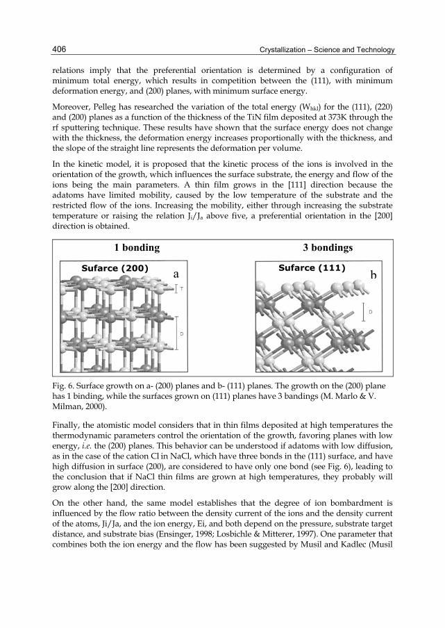
Fig. 6. Surface growth on a- (200) planes and b- (111) planes. The growth on the (200) plane has 1 binding, while the surfaces grown on (111) planes have 3 bandings (M. Marlo & V. Milman, 2000).
Finally, the atomistic model considers that in thin films deposited at high temperatures the thermodynamic parameters control the orientation of the growth, favoring planes with low energy, i.e. the (200) planes. This behavior can be understood if adatoms with low diffusion, as in the case of the cation Cl in NaCl, which have three bonds in the (111) surface, and have high diffusion in surface (200), are considered to have only one bond (see Fig. 6), leading to the conclusion that if NaCl thin films are grown at high temperatures, they probably will grow along the [200] direction.
On the other hand, the same model establishes that the degree of ion bombardment is influenced by the flow ratio between the density current of the ions and the density current of the atoms, Ji/Ja, and the ion energy, Ei, and both depend on the pressure, substrate target distance, and substrate bias (Ensinger, 1998; Losbichle & Mitterer, 1997). One parameter that combines both the ion energy and the flow has been suggested by Musil and Kadlec (Musil
Thin Film Growth Through Sputtering Technique and Its Applications
407
& Kadlec, 1990), Ziemann and Kay for Pd coatings (Ziemann and Kay, 1993) and passivation for CBN films (Kulisch, et al.,1999). This represents the energy deposited per dense particle. This bombardment-induced mobility parameter, known as the energy parameter Ep, is defined as:
ip i
a
JE E
J (4)
where Ei is incident energy of the ions and is obtained from the plasma potential (Vp) and substrate bias (Vs) and the elementary charge by the expression ( )i s pE e V V .
3.1 Physical mechanisms of thin film growth
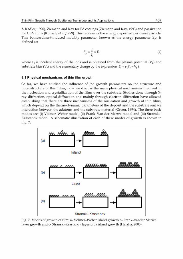
So far, we have studied the influence of the growth parameters on the structure and microstructure of thin films; now we discuss the main physical mechanisms involved in the nucleation and crystallization of the films over the substrate. Studies done through X-ray diffraction, optical diffraction and mainly through electron diffraction have allowed establishing that there are three mechanisms of the nucleation and growth of thin films, which depend on the thermodynamic parameters of the deposit and the substrate surface interaction between the adatoms and the substrate material (Green, 1994). The three basic modes are: (i) Volmer–Weber model, (ii) Frank–Van der Merwe model and (iii) Stranski–Krastanov model. A schematic illustration of each of these modes of growth is shown in Fig. 7.
Fig. 7. Modes of growth of film: a- Volmer–Weber island growth b- Frank–vander Merwe layer growth and c- Stranski-Krastanov layer plus island growth (Harsha, 2005).

Crystallization – Science and Technology
408
In the Volmer–Weber model, equilibrium exists in a three-dimensional crystal of the film in contact with the substrate, while the rest of the substrate is devoid of any condensed phase. Nucleation of film occurs in the form of discrete three-dimensional nuclei on the surface of the substrate, for example lead on graphite. Both the number of nuclei and the size of a given nucleus increase. Finally, the nuclei grow in size until they intersperse with each other to form a continuous film.
In the Frank and Vander Merwe model, nucleation occurs in the form of a monolayer island of the deposit. Eventually the monolayer’s grow together to form a complete continuous monolayer of the deposit. The process repeats itself so that the deposit grows in a layer-by-layer manner, for example rare gases on graphite. In this growth, the interaction between the substrate and the layer atoms is stronger than that between neighboring layer atoms. Layer-by-layer growth is hindered by elastic constraints at the solid–solid interface.
The Stransky and Krastanov (S-K) model combines the features of layer-by-layer growth and discrete three-dimensional nucleation The S-K nucleation is common with metal-on-metal deposition and at low temperatures where the surface mobility is low (Greene, 1987). The conditions for these types of growth are generally described in terms of thermodynamics and surface energy considerations. In this model, nucleation and growth occurs as in the layer-by-layer mode, so that a finite number of monolayer’s is produced. Subsequent formation of film occurs by formation of discrete nuclei. The lattice mismatch between the substrate and the deposit cannot be accommodated when the layer thickness increases, so the three-dimensional growth follows the layer-by-layer growth. Alternatively, symmetry or orientation of the overlayers with respect to the substrate might be responsible for the production of this growth mode.
The foregoing models were summarized by Barna and Adamik (Barna & Adamimik, 1998), who established that the growth of the films has the following evolution: nucleation, island growth, coalescence of islands, formation of polycrystalline islands and channels, development of continuous structure, and thickness growth.
According to Barna, the nucleation starting the growth of individual islands takes place on the substrate surface at the very first stage of the condensation (primary nucleation) or later on the bare substrate surface area developing upon liquid-like coalescence ( secondary nucleation). A peculiar case of nucleation shows up on the surface of a growing crystal when its growth is blocked by a surface covering layer (SCL) of an impurity phase. This is the repeated nucleation. The primary nucleation starts the condensation and the film growth on the whole substrate surface simultaneously, while the secondary and the repeated nucleation initiates the start of the growth locally in later stages of film formation. It is important to note that on amorphous substrates the nuclei are randomly oriented.
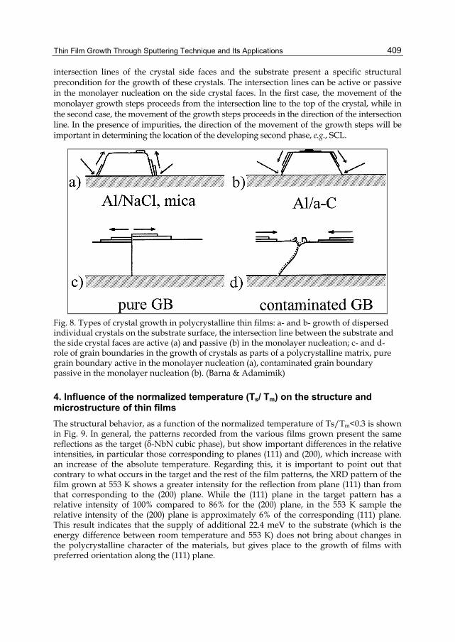
Crystal growth is the fundamental structure-forming phenomenon which incorporates the depositing material into the condensed phase. Two main cases of crystal growth should be considered in the case of polycrystalline thin films: a- the growth of discrete crystals dispersed on the substrate surface, (Fig. 8a and b), and b- the growth of crystals which are parts of a polycrystalline structure (Fig. 8c and d). Crystals growing from the nuclei are randomly oriented due to the random orientation of the nuclei. The complete coalescence of the crystals touching each other produces a grain coarsening, resulting also in the development of discrete single crystals and is connected to some changes in the orientation controlled mainly by the minimization of the substrate–crystal interface energy. The
Thin Film Growth Through Sputtering Technique and Its Applications
409
intersection lines of the crystal side faces and the substrate present a specific structural precondition for the growth of these crystals. The intersection lines can be active or passive in the monolayer nucleation on the side crystal faces. In the first case, the movement of the monolayer growth steps proceeds from the intersection line to the top of the crystal, while in the second case, the movement of the growth steps proceeds in the direction of the intersection line. In the presence of impurities, the direction of the movement of the growth steps will be important in determining the location of the developing second phase, e.g., SCL.
Fig. 8. Types of crystal growth in polycrystalline thin films: a- and b- growth of dispersed individual crystals on the substrate surface, the intersection line between the substrate and the side crystal faces are active (a) and passive (b) in the monolayer nucleation; c- and d- role of grain boundaries in the growth of crystals as parts of a polycrystalline matrix, pure grain boundary active in the monolayer nucleation (a), contaminated grain boundary passive in the monolayer nucleation (b). (Barna & Adamimik)
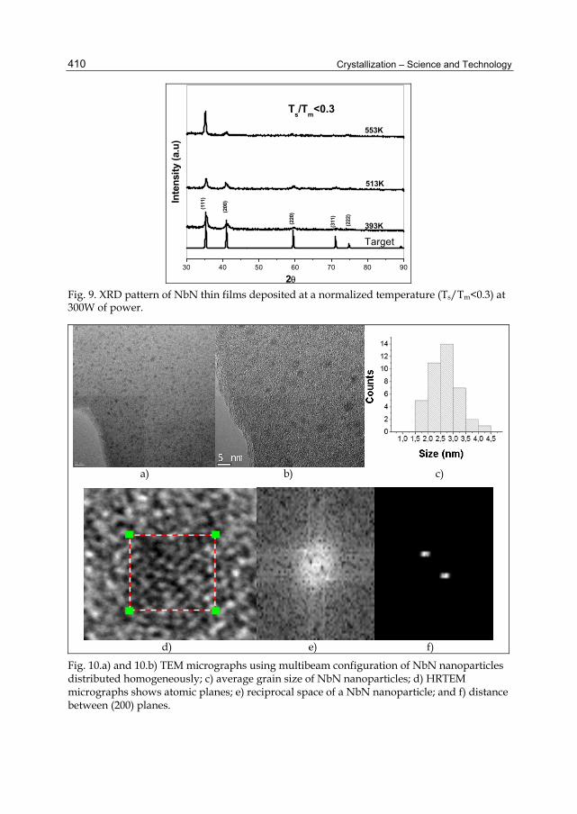
4. Influence of the normalized temperature (Ts/ Tm) on the structure and microstructure of thin films
The structural behavior, as a function of the normalized temperature of Ts/Tm<0.3 is shown in Fig. 9. In general, the patterns recorded from the various films grown present the same reflections as the target (δ-NbN cubic phase), but show important differences in the relative intensities, in particular those corresponding to planes (111) and (200), which increase with an increase of the absolute temperature. Regarding this, it is important to point out that contrary to what occurs in the target and the rest of the film patterns, the XRD pattern of the film grown at 553 K shows a greater intensity for the reflection from plane (111) than from that corresponding to the (200) plane. While the (111) plane in the target pattern has a relative intensity of 100% compared to 86% for the (200) plane, in the 553 K sample the relative intensity of the (200) plane is approximately 6% of the corresponding (111) plane. This result indicates that the supply of additional 22.4 meV to the substrate (which is the energy difference between room temperature and 553 K) does not bring about changes in the polycrystalline character of the materials, but gives place to the growth of films with preferred orientation along the (111) plane.
Crystallization – Science and Technology
410
30 40 50 60 70 80 90
Inte
nsi
ty (
a.u
)
Target
2
Ts/T
m<0.3
393K
513K
553K
(111
)
(200
)
(220
)
(311
)
(222
)
Fig. 9. XRD pattern of NbN thin films deposited at a normalized temperature (Ts/Tm<0.3) at 300W of power.
a) b) c)
d) e) f)
Fig. 10.a) and 10.b) TEM micrographs using multibeam configuration of NbN nanoparticles distributed homogeneously; c) average grain size of NbN nanoparticles; d) HRTEM micrographs shows atomic planes; e) reciprocal space of a NbN nanoparticle; and f) distance between (200) planes.

Thin Film Growth Through Sputtering Technique and Its Applications
411
Fig. 10 shows the micro-structural analysis carried out on the NbN films through transmission ion electron microcopy (TEM). Micrographs 10a and 10b correspond to the image obtained in multibeam configuration, and in them one can observe an amorphous matrix with crystalline nanoparticles with spherical morphology that are homogenously distributed along the growth plane of the film. Using Gatan software, it was determined that the average grain size of the nanoparticles was 2.7±0.6 nm with normal distribution (fig. 10c). When doing magnification of nanoparticles of Fig. 10a, we can observe an interferential pattern produced by the atoms belonging to the NbN film (fig. 9d). Higher magnifications of the nanoparticles visualized in Fig. 10a let us observe atomic planes as a product of the interferential pattern produced by the arrangement of atoms belonging to the NbN film (Fig.10d). Image processing of Fig. 10d, using the Fourier transform, lets us visualize the reciprocal space of one NbN nanoparticle (Fig. 10e). Applying a mask (Fig. 10f) over the corresponding diffracting spots and directly measuring the distance between them (0.224 nm), we can confirm that they correspond to distances between (200) planes of δ-NbN. These results confirm the analysis of XRD, which established that NbN grows preferentially along the (200) plane.
To produce thin films with normalized temperature larger than 0.3 it is necessary to have ultrahigh-vacuum equipment. This condition limits the production the thin films through magnetron sputtering. However, there are studies such as that of Frederick (Frederic & Gall, 2005), who grew CrN thin films on MgO substrate through magnetron sputtering with Ts/tm between 0 .43 to 0.48. These authors found that the films grown at 993 K present complete single-crystal structure with smooth surfaces. The root-mean-square surface roughness for 230-nm-thick layers decreases from 18.8 to 9.3 to 1.1 nm as Ts is raised from 873 to 973 to 1073 K.
4.1 Influence of the gas flow on the structure and microstructure of thin films
In a different set of experiments, nitrogen gas was introduced into the deposition chamber (maintaining the final working pressure constant) in order to study the influence that the addition of this gas during deposition exerts on the structural and micro structural properties of the NbN films. Fig. 11 shows the diffraction patterns recorded from the films grown at 300 W, 553 K and different nitrogen flows. The results obtained make clear that in all cases a preferential growth appears along the (200) plane (Fig.11a). The relative intensity of this diffraction peak is so high that it makes it impossible to distinguish the diffraction peaks corresponding to other planes. To determine the polycrystalline character of the film, we carried out X-ray diffraction experiments at grazing incidence. Fig. 11b shows a representative example. It is clear from Fig. 11 that the films show the same diffraction peaks as the target, confirming their polycrystalline character, although having a preferential orientation along the (200) plane (texture index, 0.65). The grain sizes deduced by Scherer’s equation (Cullity, 2001) for the different films grown along the (200) plane vary from 35 nm (Φ= 2 sscm) to 42 nm (Φ = 6 sscm). These results indicate that incorporation of nitrogen during the fabrication process favors the preferential growth of the d-NbN phase along the (200) plane. This effect has also been produced during the growth of TiN films, due to the change of the preferred orientation of the films from the [111] direction to the [200] direction when the gas flow is increased.
The incorporation of nitrogen during the deposition process implies changes in the dynamics of the plasma, since the increase in the number of nitrogen molecules increases the

Crystallization – Science and Technology
412
probability of collisions, promoting a larger number of chemical reactions on the substrate surface. These reactions can be explained using a model of low energy (<20 eV) ion bombardment during film growth at a Ts/Tm ratio ranging between 0.1 and 0.3 (a condition which is satisfied in this case) (Petrov & Barna, 2003). According to this model, 25 eV are sufficient to cause collision dissociation of the N2 ions, providing a continuous source of atomic nitrogen. The nitrogen readily chemisorbs on the (200) planes but not on the N-terminated (111) planes. This in turn reduces the mean free path of the metal cation on the (200) plane due to capture by the nitrogen atoms, and promotes the formation of a NbNi
30 40 50 60 70 80 90
a
(222
)
(311
)
(220
)
(111
)
2
Inte
nsi
ty (
a.u
)
=2 sccm
=4 sccm
=6 sccm
Target
(200
)
30 40 50 60 70 80 90
b
Target
= 6 sccm
(222
)
(311
)
(220
)
(11
1)(2
00)
Inte
nsi
ty(a
.u)
2
Fig. 11. a) XRD patterns -2 configuration and b) Grazing angle (2) XRD pattern recorder from the NbN film, grown at 300 W, 553 K, 20 sccm of Ar and 6 sccm of N2.
Thin Film Growth Through Sputtering Technique and Its Applications
413
(i = 1–4) admolecule or islands of adatoms (Petrov & Barna, 2003). This can be considered as causing an additional decrease in the (200) surface energy relative to that of the (111) plane. Consequently, the presence of the nitrogen atoms reduces the flow of cations from the (200) to the (111) planes, resulting in the orientation of the growth along the [200] direction. In this example, the growth of the films depends on the final working pressure as well as the bombardment energy of the ions.
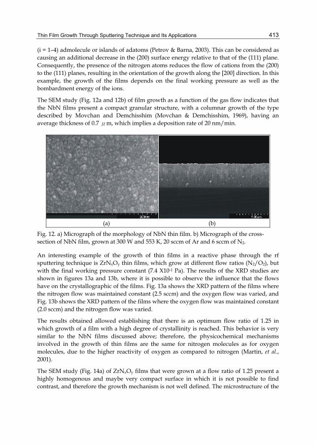
The SEM study (Fig. 12a and 12b) of film growth as a function of the gas flow indicates that the NbN films present a compact granular structure, with a columnar growth of the type described by Movchan and Demchisshim (Movchan & Demchisshim, 1969), having an average thickness of 0.7 μm, which implies a deposition rate of 20 nm/min.
(a) (b)
Fig. 12. a) Micrograph of the morphology of NbN thin film. b) Micrograph of the cross- section of NbN film, grown at 300 W and 553 K, 20 sccm of Ar and 6 sccm of N2.
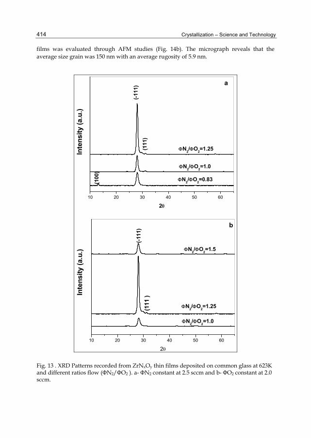
An interesting example of the growth of thin films in a reactive phase through the rf sputtering technique is ZrNxOy thin films, which grow at different flow ratios (N2/O2), but with the final working pressure constant (7.4 X10⁻¹ Pa). The results of the XRD studies are shown in figures 13a and 13b, where it is possible to observe the influence that the flows have on the crystallographic of the films. Fig. 13a shows the XRD pattern of the films where the nitrogen flow was maintained constant (2.5 sccm) and the oxygen flow was varied, and Fig. 13b shows the XRD pattern of the films where the oxygen flow was maintained constant (2.0 sccm) and the nitrogen flow was varied.
The results obtained allowed establishing that there is an optimum flow ratio of 1.25 in which growth of a film with a high degree of crystallinity is reached. This behavior is very similar to the NbN films discussed above; therefore, the physicochemical mechanisms involved in the growth of thin films are the same for nitrogen molecules as for oxygen molecules, due to the higher reactivity of oxygen as compared to nitrogen (Martin, et al., 2001).
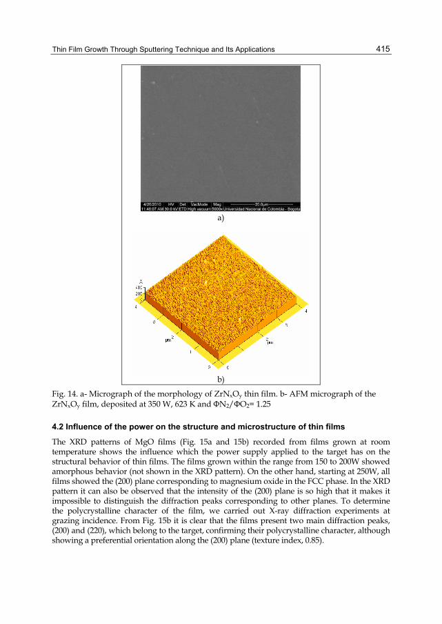
The SEM study (Fig. 14a) of ZrNxOy films that were grown at a flow ratio of 1.25 present a highly homogenous and maybe very compact surface in which it is not possible to find contrast, and therefore the growth mechanism is not well defined. The microstructure of the
Crystallization – Science and Technology
414
films was evaluated through AFM studies (Fig. 14b). The micrograph reveals that the average size grain was 150 nm with an average rugosity of 5.9 nm.
10 20 30 40 50 60
a
N2/O
2=0.83
N2/O
2=1.25
N2/O
2=1.0
(111
)
(100
)
(-11
1)
Inte
nsi
ty (
a.u
.)
2
10 20 30 40 50 60
b
N2/O
2=1.5
N2/O
2=1.25
N2/O
2=1.0
(111
)(-
111)
Inte
nsi
ty (
a.u
.)
2
Fig. 13 . XRD Patterns recorded from ZrNxOy thin films deposited on common glass at 623K and different ratios flow (ΦN2/ΦO2 ). a- ΦN2 constant at 2.5 sccm and b- ΦO2 constant at 2.0 sccm.
Thin Film Growth Through Sputtering Technique and Its Applications
415
a)
b)
Fig. 14. a- Micrograph of the morphology of ZrNxOy thin film. b- AFM micrograph of the ZrNxOy film, deposited at 350 W, 623 K and ΦN2/ΦO2= 1.25
4.2 Influence of the power on the structure and microstructure of thin films
The XRD patterns of MgO films (Fig. 15a and 15b) recorded from films grown at room temperature shows the influence which the power supply applied to the target has on the structural behavior of thin films. The films grown within the range from 150 to 200W showed amorphous behavior (not shown in the XRD pattern). On the other hand, starting at 250W, all films showed the (200) plane corresponding to magnesium oxide in the FCC phase. In the XRD pattern it can also be observed that the intensity of the (200) plane is so high that it makes it impossible to distinguish the diffraction peaks corresponding to other planes. To determine the polycrystalline character of the film, we carried out X-ray diffraction experiments at grazing incidence. From Fig. 15b it is clear that the films present two main diffraction peaks, (200) and (220), which belong to the target, confirming their polycrystalline character, although showing a preferential orientation along the (200) plane (texture index, 0.85).
Crystallization – Science and Technology
416
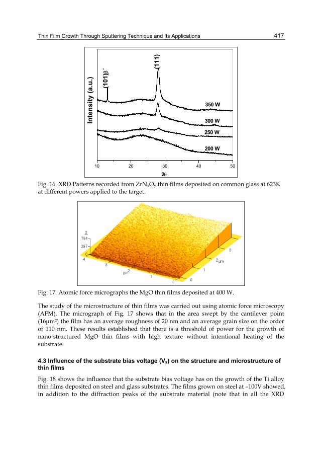
Another example that shows the influence of the power supply applied to the target on the crystallization of the films is the growth of ZrNxOy thin films; the films were grown from the Zr target in the reactive phase in an atmosphere of nitrogen and oxygen (ΦN= 2.5 sccm, ΦO=2.0 sccm). In the XRD pattern of Fig. 16, it is possible to determine that there is a threshold power (250W) for producing the crystallization of the film on the substrate. At this power, the film grows with a high degree of crystallization along the (111) plane. This behavior can be explained by the energy model, since increasing the power on the target implies increasing the energy of the ions that are bombarding the substrate and therefore improving the mobility of the adatoms, which produce chemical reactions and atomic grouping along the planes with the higher surface energy, which generates films with a high degree of crystallinity.
30 40 50 60 70 80
a
(220
)
(200
)
400W
350W
300W
250W
MgO
Inte
nsi
ty (
a.u
.)
2
30 40 50 60 70 80
b
(220
)
(200
)
(111
)
400W
MgO Target
Inte
nsi
ty (
u.a
.)
2
Fig. 15. a- XRD patterns recorded from MgO films deposited at 293 K and different power supplies applied to the target b- Grazing angle (3) XRD pattern recorded from a MgO film grown at 400 W. The target XRD pattern is included as reference.
Thin Film Growth Through Sputtering Technique and Its Applications
417
10 20 30 40 50
(111
)
(101
)´
350 W
300 W
250 W
200 W
Inte
nsi
ty (
a.u
.)
2 Fig. 16. XRD Patterns recorded from ZrNxOy thin films deposited on common glass at 623K at different powers applied to the target.
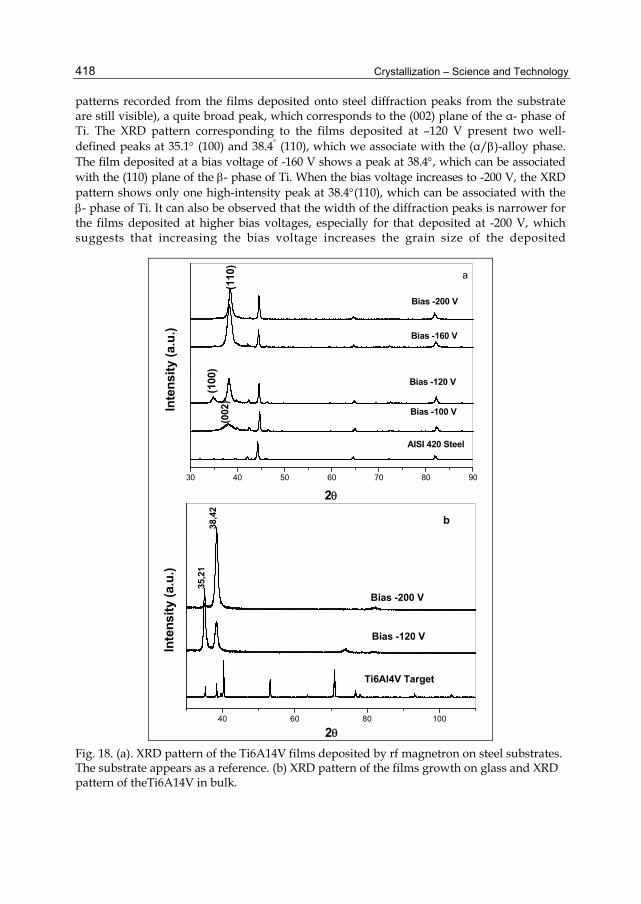
Fig. 17. Atomic force micrographs the MgO thin films deposited at 400 W.
The study of the microstructure of thin films was carried out using atomic force microscopy (AFM). The micrograph of Fig. 17 shows that in the area swept by the cantilever point (16μm2) the film has an average roughness of 20 nm and an average grain size on the order of 110 nm. These results established that there is a threshold of power for the growth of nano-structured MgO thin films with high texture without intentional heating of the substrate.
4.3 Influence of the substrate bias voltage (Vs) on the structure and microstructure of thin films
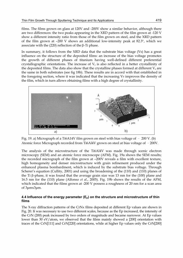
Fig. 18 shows the influence that the substrate bias voltage has on the growth of the Ti alloy thin films deposited on steel and glass substrates. The films grown on steel at –100V showed, in addition to the diffraction peaks of the substrate material (note that in all the XRD
Crystallization – Science and Technology
418
patterns recorded from the films deposited onto steel diffraction peaks from the substrate are still visible), a quite broad peak, which corresponds to the (002) plane of the α- phase of Ti. The XRD pattern corresponding to the films deposited at –120 V present two well-defined peaks at 35.1 (100) and 38.4 (110), which we associate with the (α/)-alloy phase. The film deposited at a bias voltage of -160 V shows a peak at 38.4, which can be associated with the (110) plane of the - phase of Ti. When the bias voltage increases to -200 V, the XRD pattern shows only one high-intensity peak at 38.4(110), which can be associated with the - phase of Ti. It can also be observed that the width of the diffraction peaks is narrower for the films deposited at higher bias voltages, especially for that deposited at -200 V, which suggests that increasing the bias voltage increases the grain size of the deposited
30 40 50 60 70 80 90
a
(002
)(1
00)
(110
)
AISI 420 Steel
Bias -200 V
Bias -160 V
Bias -100 V
Bias -120 V
Inte
nsi
ty (
a.u
.)
2
40 60 80 100
b
35,2
138
,42
Ti6Al4V Target
Bias -200 V
Bias -120 V
Inte
nsi
ty (
a.u
.)
2
Fig. 18. (a). XRD pattern of the Ti6A14V films deposited by rf magnetron on steel substrates. The substrate appears as a reference. (b) XRD pattern of the films growth on glass and XRD pattern of theTi6A14V in bulk.
Thin Film Growth Through Sputtering Technique and Its Applications
419
films. The films grown on glass at 120V and -200V show a similar behavior, although there are two differences: the two peaks appearing in the XRD pattern of the film grown at -120 V show a different intensity ratio from those of the film grown on steel, and the XRD pattern of the film grown at –200 V shows an additional low-intensity peak at 82.3, which we associate with the (220) reflection of the -Ti phase.
In summary, it follows from the XRD data that the substrate bias voltage (Vs) has a great influence on the structure of the deposited films: an increase of the bias voltage promotes the growth of different phases of titanium having well-defined different preferential crystallographic orientations. The increase of Vs is also reflected in a better crystallinity of the deposited films. The data also show that the crystalline phases formed at different Vs are the same in both substrates (see fig 18b). These results are in accord with that established in the foregoing section, where it was indicated that the increasing Vs improves the density of the film, which in turn allows obtaining films with a high degree of crystallinity.
Fig. 19. a) Micrograph of a Ti6A14V film grown on steel with bias voltage of – 200 V. (b) Atomic force Micrograph recorded from Ti6Al4V grown on steel at bias voltage of –200V.
The analysis of the microstructure of the Ti6Al4V was made through scenic electron microscopy (SEM) and an atomic force microscope (AFM). Fig. 19a shows the SEM results; the recorded micrograph of the film grown at –200V reveals a film with excellent texture, high homogeneity and denser microstructure with grain refinement produced under the enhanced plasma bombardment, which is induced by the substrate bias voltage. Through Scherer’s equation (Cullity, 2001) and using the broadening of the (110) and (110) planes of the Ti -phase, it was found that the average grain size was 13 nm for the (100) plane and 16.5 nm for the (110) plane (Alfonso et al., 2005). Fig. 19b shows the results of the AFM, which indicated that the films grown at -200 V possess a roughness of 20 nm for a scan area of 3μmx3μm.
4.4 Influence of the energy parameter (Ep) on the structure and microstructure of thin films
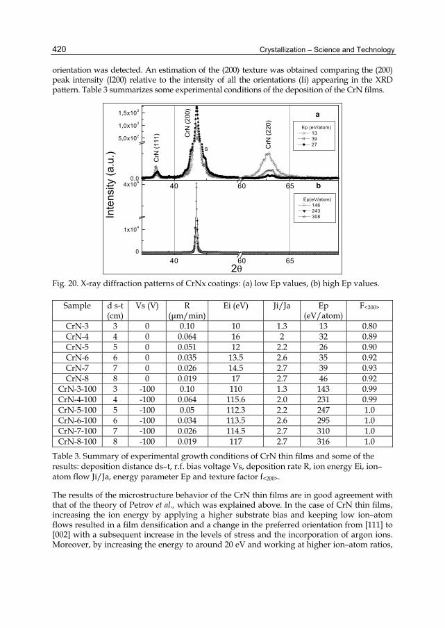
The X-ray diffraction patterns of the CrNx films deposited at different Ep values are shown in Fig. 20. It was necessary to use two different scales, because as the Ep increased, the intensity of the CrN (200) peak increased by two orders of magnitude and became narrower. At Ep values lower than 30 eV/atom, we observed that the films mainly showed a [200] orientation with traces of the CrN[111] and CrN[220] orientations, while at higher Ep values only the CrN[200]
a) b)
μm
Ǻ
0 1
2 μm
3
0
1
2
3
607
1174
Crystallization – Science and Technology
420
orientation was detected. An estimation of the ⟨200⟩ texture was obtained comparing the (200) peak intensity (I200) relative to the intensity of all the orientations (Ii) appearing in the XRD pattern. Table 3 summarizes some experimental conditions of the deposition of the CrN films.
40 60 650
1x10⁴
4x10⁴b
Inte
nsity
(a.
u.)
2
Ep(eV/atom) 146 243 308
40 60 650,0
5,0x10²
1,0x10³
1,5x10³
a
CrN
(2
20
)
s
CrN
(2
00
)
CrN
(1
11
)
Ep (eV/atom) 13 39 27
Fig. 20. X-ray diffraction patterns of CrNx coatings: (a) low Ep values, (b) high Ep values.
Sample d s-t(cm)
Vs (V) R(μm/min)
Ei (eV) Ji/Ja Ep (eV/atom)
F<200>
CrN-3 3 0 0.10 10 1.3 13 0.80 CrN-4 4 0 0.064 16 2 32 0.89 CrN-5 5 0 0.051 12 2.2 26 0.90 CrN-6 6 0 0.035 13.5 2.6 35 0.92 CrN-7 7 0 0.026 14.5 2.7 39 0.93 CrN-8 8 0 0.019 17 2.7 46 0.92
CrN-3-100 3 -100 0.10 110 1.3 143 0.99 CrN-4-100 4 -100 0.064 115.6 2.0 231 0.99 CrN-5-100 5 -100 0.05 112.3 2.2 247 1.0 CrN-6-100 6 -100 0.034 113.5 2.6 295 1.0 CrN-7-100 7 -100 0.026 114.5 2.7 310 1.0 CrN-8-100 8 -100 0.019 117 2.7 316 1.0
Table 3. Summary of experimental growth conditions of CrN thin films and some of the results: deposition distance ds–t, r.f. bias voltage Vs, deposition rate R, ion energy Ei, ion–atom flow Ji/Ja, energy parameter Ep and texture factor f<200>.
The results of the microstructure behavior of the CrN thin films are in good agreement with that of the theory of Petrov et al., which was explained above. In the case of CrN thin films, increasing the ion energy by applying a higher substrate bias and keeping low ion–atom flows resulted in a film densification and a change in the preferred orientation from [111] to [002] with a subsequent increase in the levels of stress and the incorporation of argon ions. Moreover, by increasing the energy to around 20 eV and working at higher ion–atom ratios,
Thin Film Growth Through Sputtering Technique and Its Applications
421
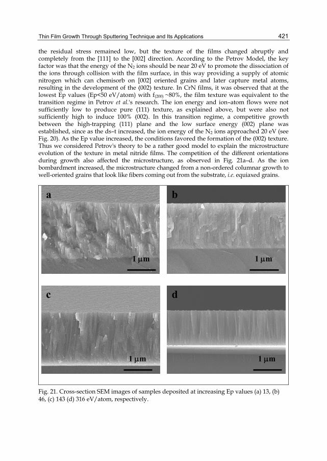
the residual stress remained low, but the texture of the films changed abruptly and completely from the [111] to the [002] direction. According to the Petrov Model, the key factor was that the energy of the N2 ions should be near 20 eV to promote the dissociation of the ions through collision with the film surface, in this way providing a supply of atomic nitrogen which can chemisorb on [002] oriented grains and later capture metal atoms, resulting in the development of the ⟨002⟩ texture. In CrN films, it was observed that at the lowest Ep values (Ep<50 eV/atom) with f(200) ~80%, the film texture was equivalent to the transition regime in Petrov et al.'s research. The ion energy and ion–atom flows were not sufficiently low to produce pure ⟨111⟩ texture, as explained above, but were also not sufficiently high to induce 100% ⟨002⟩. In this transition regime, a competitive growth between the high-trapping (111) plane and the low surface energy (002) plane was established, since as the ds–t increased, the ion energy of the N2 ions approached 20 eV (see Fig. 20). As the Ep value increased, the conditions favored the formation of the ⟨002⟩ texture. Thus we considered Petrov's theory to be a rather good model to explain the microstructure evolution of the texture in metal nitride films. The competition of the different orientations during growth also affected the microstructure, as observed in Fig. 21a–d. As the ion bombardment increased, the microstructure changed from a non-ordered columnar growth to well-oriented grains that look like fibers coming out from the substrate, i.e. equiaxed grains.
Fig. 21. Cross-section SEM images of samples deposited at increasing Ep values (a) 13, (b) 46, (c) 143 (d) 316 eV/atom, respectively.
a b
c d
1 m
1 m 1 m
1 m
Crystallization – Science and Technology
422
5. Chemical characterization of thin films
5.1 X-ray photoelectron spectroscopy (XPS) analysis
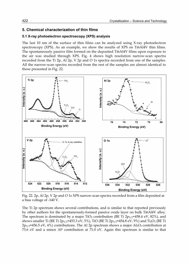
The last 10 nm of the surface of thin films can be analyzed using X-ray photoelectron spectroscopy (XPS). As an example, we show the results of XPS on Ti6Al4V thin films. The spontaneously passive film formed on the deposited Ti6Al4V films upon exposure to the air was studied through XPS. Fig. 4 shows high resolution narrow-scan spectra recorded from the Ti 2p, Al 2p, V 2p and O 1s spectra recorded from one of the samples. All the narrow-scan spectra recorded from the rest of the samples are almost identical to those presented in Fig. 22.
Fig. 22. 2p, Al 2p, V 2p and O 1s XPS narrow-scan spectra recorded from a film deposited at a bias voltage of -140 V.
The Ti 2p spectrum shows several contributions, and is similar to that reported previously by other authors for the spontaneously-formed passive oxide layer on bulk Ti6Al4V alloy. The spectrum is dominated by a major TiO2 contribution (BE Ti 2p3/2=458.4 eV, 82%), and shows smaller Ti (BE Ti 2p3/2=453.3 eV, 5%), TiO (BE Ti 2p3/2=454.8 eV, 9%) and Ti2O3 (BE Ti 2p3/2=456.5 eV, 4%) contributions. The Al 2p spectrum shows a major Al2O3 contribution at 73.6 eV and a minor Al0 contribution at 71.0 eV. Again this spectrum is similar to that
Thin Film Growth Through Sputtering Technique and Its Applications
423
observed for the passive oxide layer on a Ti6Al4V alloy. The O 1s peak shows three different contributions: a main one at 530.2 eV that can be associated with metal-oxygen bonds, and two much less intense contributions at 531.7 eV and 532.8 eV, which correspond to the presence of OH- groups and chemisorbed water, respectively. The fit of the V 2p spectrum is complicated by the fact that the V peaks overlap strongly with the O 1s K3,4 X-ray satellite peaks. Therefore, the whole spectrum was refined considering the presence of these satellites and the presence of vanadium peaks. The results show the presence of an intense peak at 515.4 eV, which we associate with the presence of VO2, and a less intense vanadium contribution at 516.7 eV, which corresponds to V2O5. This finding contrasts with those of Milosev (Milosev et al., 2000), who did not find oxidized vanadium in the passive layer formed on bulk Ti6Al4V (Alfonso et al., 2006).
These results show that the films that have been grown through rf magnetron sputtering reproduced the stiochoimetry of the target, although on the surface of the thin films chemical reactions will be produced, forming hydroxides and passivation layers.
5.2 Energy dispersive X-ray (EDX) analysis
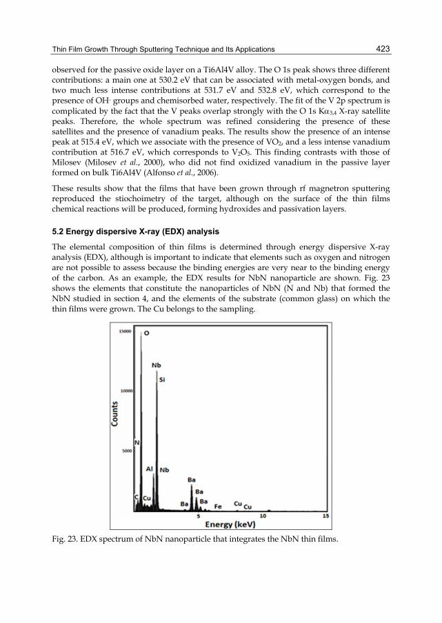
The elemental composition of thin films is determined through energy dispersive X-ray analysis (EDX), although is important to indicate that elements such as oxygen and nitrogen are not possible to assess because the binding energies are very near to the binding energy of the carbon. As an example, the EDX results for NbN nanoparticle are shown. Fig. 23 shows the elements that constitute the nanoparticles of NbN (N and Nb) that formed the NbN studied in section 4, and the elements of the substrate (common glass) on which the thin films were grown. The Cu belongs to the sampling.
Fig. 23. EDX spectrum of NbN nanoparticle that integrates the NbN thin films.
Crystallization – Science and Technology
424
6. Optical characterization of thin films
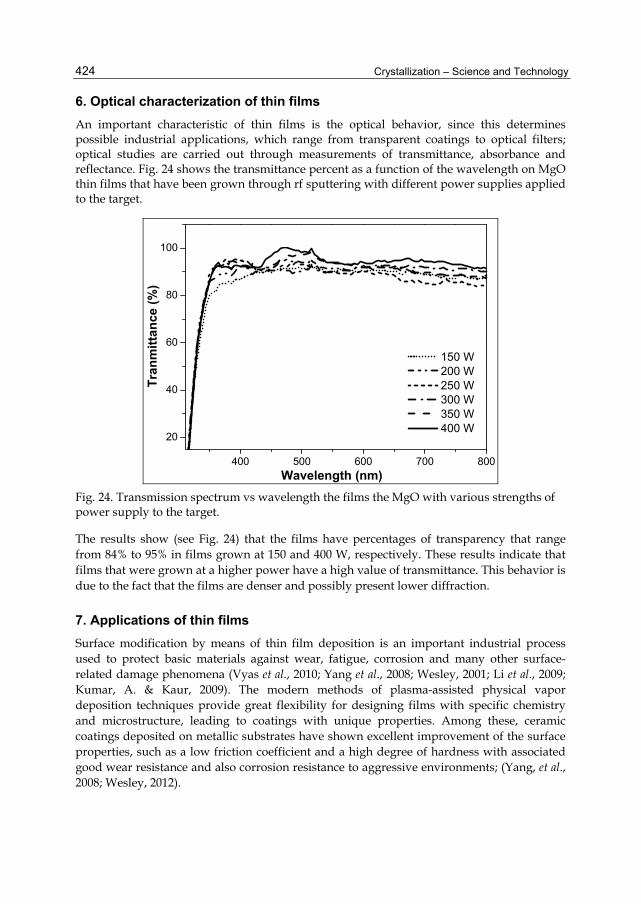
An important characteristic of thin films is the optical behavior, since this determines possible industrial applications, which range from transparent coatings to optical filters; optical studies are carried out through measurements of transmittance, absorbance and reflectance. Fig. 24 shows the transmittance percent as a function of the wavelength on MgO thin films that have been grown through rf sputtering with different power supplies applied to the target.
400 500 600 700 800
20
40
60
80
100
150 W 200 W 250 W 300 W 350 W 400 W
Tra
nm
itta
nce
(%
)
Wavelength (nm) Fig. 24. Transmission spectrum vs wavelength the films the MgO with various strengths of power supply to the target.
The results show (see Fig. 24) that the films have percentages of transparency that range from 84% to 95% in films grown at 150 and 400 W, respectively. These results indicate that films that were grown at a higher power have a high value of transmittance. This behavior is due to the fact that the films are denser and possibly present lower diffraction.
7. Applications of thin films
Surface modification by means of thin film deposition is an important industrial process used to protect basic materials against wear, fatigue, corrosion and many other surface-related damage phenomena (Vyas et al., 2010; Yang et al., 2008; Wesley, 2001; Li et al., 2009; Kumar, A. & Kaur, 2009). The modern methods of plasma-assisted physical vapor deposition techniques provide great flexibility for designing films with specific chemistry and microstructure, leading to coatings with unique properties. Among these, ceramic coatings deposited on metallic substrates have shown excellent improvement of the surface properties, such as a low friction coefficient and a high degree of hardness with associated good wear resistance and also corrosion resistance to aggressive environments; (Yang, et al., 2008; Wesley, 2012).
Thin Film Growth Through Sputtering Technique and Its Applications
425
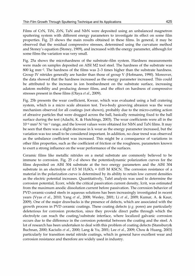
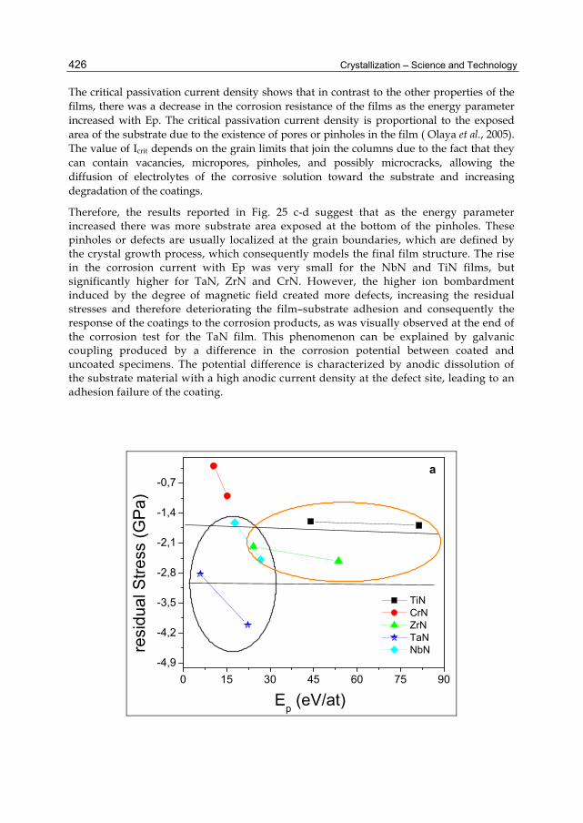
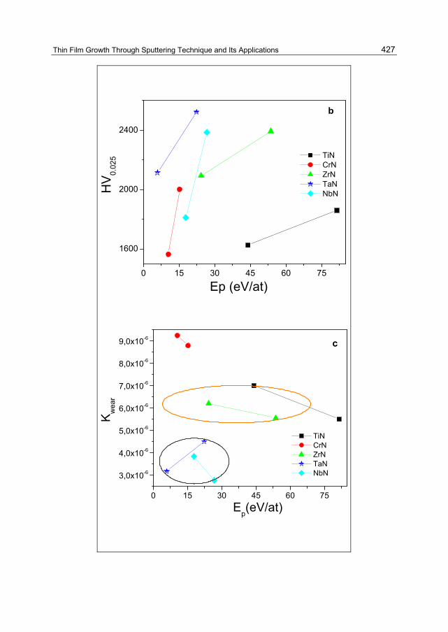
Films of CrN, TiN, ZrN, TaN and NbN were deposited using an unbalanced magnetron sputtering system with different energy parameters to investigate its effect on some film properties. Fig. 23 shows the main results obtained in these films. In general, it may be observed that the residual compressive stresses, determined using the curvature method and Stoney’s equation (Stoney, 1909), and increased with the energy parameter, although for some films the variation was very small.
Fig. 25a shows the microhardness of the substrate–film system. Hardness measurements were made on samples deposited on AISI M2 tool steel. The hardness of the substrate was 800 kg mm−2. The hardness of the films was 2–3 times higher than the substrate hardness. Group IV nitrides generally are harder than those of group V (Hofmann, 1990). Moreover, the data showed that the hardness increased as the energy parameter increased. This could be attributed to the increase in ion bombardment on the substrate surface, increasing adatom mobility and producing denser films, and the effect on hardness of compressive stresses present in these films (Olaya et al., 2009).
Fig. 25b presents the wear coefficient, Kwear, which was evaluated using a ball cratering system, which is a micro scale abrasion test. Two-body grooving abrasion was the wear mechanism observed for all coatings (not shown), probably due to the micro-cutting action of abrasive particles that were dragged across the ball, basically remaining fixed to the ball surface during the test (Adachi, K. & Hutchings, 2003). The wear coefficients were all in the 10−6 mm3 N−1m−1 range, and the lowest values were obtained for NbN and TaN films. It may be seen that there was a slight decrease in k wear as the energy parameter increased, but the variation was too small to be considered important. In addition, no clear trend was observed as the unbalance coefficient was increased. This might be a consequence of variations in other film properties, such as the coefficient of friction or the roughness, parameters known to exert a strong influence on the wear performance of the surfaces.
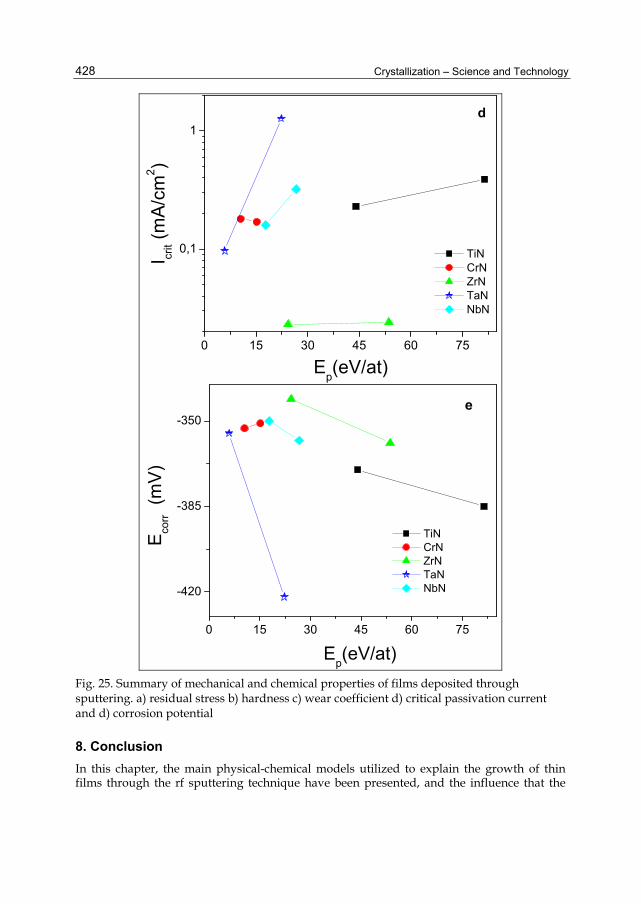
Ceramic films like metallic nitrides on a metal substrate are commonly believed to be immune to corrosion. Fig. 25 c-d shows the potentiodynamic polarization curves for the films deposited on AISI 304 substrate at the two energy parameters and the AISI 304 substrate in an electrolyte of 0.5 M H2SO4 + 0.05 M KSCN. The corrosion resistance of a material in the polarization curve is determined by its ability to retain low current densities as the electric potential increases. Quantitatively, Tafel analysis was used to determine the corrosion potential, Ecorr, while the critical passivation current density, Icrit, was estimated from the maximum anodic dissolution current before passivation. The corrosion behavior of PVD ceramic-coated steels in aqueous solutions has been increasingly investigated in recent years (Vyas et al., 2010; Yang et al., 2008; Wesley, 2001; Li et al., 2009; Kumar, A. & Kaur, 2009). One of the major drawbacks is the presence of defects, which are associated with the growth process in PVD ceramic coatings. These coating defects (e.g. pores) are particularly deleterious for corrosion protection, since they provide direct paths through which the electrolyte can reach the coating/substrate interface, where localized galvanic corrosion occurs due to the difference in the corrosion potential between the coating and the steel. A lot of research has been undertaken to deal with this problem of coating defects (Stansbury& Buchnan, 2000; Kaciulis et al., 2000; Lang & Yu, 2001; Lee et al., 2009; Chou & Huang, 2003) particularly for transition metal nitride coatings, which in general have excellent wear and corrosion resistance and therefore are widely used in industry.
Crystallization – Science and Technology
426
The critical passivation current density shows that in contrast to the other properties of the films, there was a decrease in the corrosion resistance of the films as the energy parameter increased with Ep. The critical passivation current density is proportional to the exposed area of the substrate due to the existence of pores or pinholes in the film ( Olaya et al., 2005). The value of Icrit depends on the grain limits that join the columns due to the fact that they can contain vacancies, micropores, pinholes, and possibly microcracks, allowing the diffusion of electrolytes of the corrosive solution toward the substrate and increasing degradation of the coatings.
Therefore, the results reported in Fig. 25 c-d suggest that as the energy parameter increased there was more substrate area exposed at the bottom of the pinholes. These pinholes or defects are usually localized at the grain boundaries, which are defined by the crystal growth process, which consequently models the final film structure. The rise in the corrosion current with Ep was very small for the NbN and TiN films, but significantly higher for TaN, ZrN and CrN. However, the higher ion bombardment induced by the degree of magnetic field created more defects, increasing the residual stresses and therefore deteriorating the film–substrate adhesion and consequently the response of the coatings to the corrosion products, as was visually observed at the end of the corrosion test for the TaN film. This phenomenon can be explained by galvanic coupling produced by a difference in the corrosion potential between coated and uncoated specimens. The potential difference is characterized by anodic dissolution of the substrate material with a high anodic current density at the defect site, leading to an adhesion failure of the coating.
0 15 30 45 60 75 90
-4,9
-4,2
-3,5
-2,8
-2,1
-1,4
-0,7a
resi
dual
Str
ess
(GP
a)
Ep (eV/at)
TiN CrN ZrN TaN NbN
Thin Film Growth Through Sputtering Technique and Its Applications
427
0 15 30 45 60 75
1600
2000
2400
bH
V0.
025
Ep (eV/at)
TiN CrN ZrN TaN NbN
0 15 30 45 60 75
3,0x10⁻⁶
4,0x10⁻⁶
5,0x10⁻⁶
6,0x10⁻⁶
7,0x10⁻⁶
8,0x10⁻⁶
9,0x10⁻⁶c
Kw
ear
Ep(eV/at)
TiN CrN ZrN TaN NbN
Crystallization – Science and Technology
428
0 15 30 45 60 75
0,1
1d
I crit
(mA
/cm
2 )
Ep(eV/at)
TiN CrN ZrN TaN NbN
0 15 30 45 60 75
-420
-385
-350e
Eco
rr
(mV
)
Ep(eV/at)
TiN CrN ZrN TaN NbN
Fig. 25. Summary of mechanical and chemical properties of films deposited through sputtering. a) residual stress b) hardness c) wear coefficient d) critical passivation current and d) corrosion potential
8. Conclusion
In this chapter, the main physical-chemical models utilized to explain the growth of thin films through the rf sputtering technique have been presented, and the influence that the
Thin Film Growth Through Sputtering Technique and Its Applications
429
growth parameters have on the crystallinity and the micro-structure of the thin films has been discussed, and based on the described models, examples have been provided of the thin films’ growth under each of the growth parameters. The fundamental idea of presenting these basic theories is to introduce the science of materials to young researchers in the world, helping them to understand by means of examples the basic concepts that apply to the growth of thin films, with the hope that a better understanding of these theories will produce new and better applications.
9. References
Adachi, K. & Hutchings, I., Wear-mode mapping for the micro-scale abrasion test. Wear, Vol 255, issues 1-6, (august-september 2003) 23-29.
B. A. Movchan and A. V. Demchishin, Study of the Structure and Properties of Dioxide thin, Fiz. Met. Metalloved. Vol. 28, (1969) 83-90.
B. D. Cullity, s: R. Stock, Elements of X-ray diffraction, Prentice Hall, 2001. B. Rauschenbach, J. W. Gerlach, Texture Development in Titanium Nitride Films Grown by
Low-Energy Ion Assisted Deposition, Cryst. Res. Technol. Vol. 35, (2000) 6-7. B. Wang, Y.N. Zhao, Z. He, The effects of deposition parameters on the crystallographic
orientation of AIN films prepared by RF reactive sputtering, Vacuum. Vol. 48, (1997) 427-429.
B. Window & N. Savvides, Charged particle fluxes from planar magnetron sputtering sources, J. Vac. Sci. Technol. A4 (1986) 196–202
Barna, P. , Adamik, M., Fundamental structure forming phenomena of polycrystalline films and the structure zone models. Thin Solid Films, Vol. 317, (April 1998) 27-33.
C. Lin, C. Lee, Growth of Tantalum Nitride Films on Si by Radio Frequency Reactive Sputtering of Ta in N2/Ar Gas Mixtures: Effect of Bias, J. Electrochem. Soc. Vol. 147, (2000) 713-718.
C. S. Shin, D. Gall, Y. W. Kim, N. Hellgren, I. Petrov, J.E. Greene, Development of preferred orientation in polycrystalline NaCl-structure δ-TaN layers grown by reactive magnetron sputtering: Role of low-energy ion surface interactions , J. Appl. Phys. 92, (2002) 5084.
C.R. Weissmantel, Deposition of Metastable Films by Ion Beam and Plasma Techniques, Proc. 9th Int. Vacuum Congress and 5th Int. Conf. on Solid Surfaces (Madrid), 26 Sept-1 Oct 1983, p 229-308
Chou, W., Yu, G. & Huang, J. Corrosion resistance of ZrN films on AISI 304 stainless steel substrate. Surface and Coatings Technology. Vol. 167, issue 1, (april 2003) 59-67.
Emery, C., Chourasia,A., Yashar, P., A study of CrNx thin films by X-ray photoelectron spectroscopy J. Elect. Spectros. Relat. Phenom. Vol. 104, issue 1-3, (July 1999) 91-97.
Flores, J. F.; Olaya, J. J.; Colás, R.; Rodil, S. E.; Valdez, B. S.; Fuente, I. G. Corrosion behaviour of TaN thin PVD films on steels. Corrosion Engineering, Science and Tecjnology, Vol. 4, issue 2, (June 2006) 168-176.
G. G. Stoney, The measurement of stress in layered structures, in: Proc. Roy. Soc. London Vol. A82, (1909) 172.
G. Kamath , A.P. Ehiasarian, Y. Purandare, P.Eh. Hovsepian, Tribological and oxidation behaviour of TiAlCN/VCN nanoscale multilayer coating deposited by the combined HIPIMS/(HIPIMS-UBM) technique, Surface & Coatings Technology 205 (2011) 2823–2829
Goldfarb, I., Pelleg, J., Zevin, L. and Croitoru, N. (1991). Lattice distortion in thin films of IVB metal (Ti, Zr, Hr) Nitrides, Thin Solid Film, Vol. 200, issue 1, (May 1991) 117-127., (May 1991), 117-127.
Crystallization – Science and Technology
430
Greene, J. E., Low Energy Ion Bombardment during Film Deposition from the Vapor Phase: Effects on Microstructure and Microchemistry, Solid State Technol., 30,(4), (1987)115.
Greene, J. E., Nucleation, Film Growth, and Microstructural Evolution, Deposition Processes for Films and Coating, 2nd edition, (R. Bunshah,ed.), Ch. 13, Noyes Publications (1994).
H. Liu, W. Tang, D. Hui, L. Hei, F. Lu. Characterization of (Al, Si)N films deposited by balanced magnetron sputtering, Thin Solid Films, Vol. 517, issue 21, 1 (September 2009) 5988-5993.
H.B. Nie, S.Y. Xu, S.J. Wang, L.P. You, Z. Yang, C.K. Ong, J. Li and T.Y.F. Liew, Structural and electrical properties of tantalum nitride thin films fabricated by using reactive radio-frequency magnetron sputtering, Appl. Phys. A. Mater. Sci. process, Vol. 73 (2001) 229- 236.
Hofmann S., Target and substrate surface reaction kinetics in magnetron sputtering of nitride coatings, Thin Solid Films, Vol. 191, (1990) 335-348.
Hwan-Chul Leea, Guen-Hong Kimb, Soon-Ku Hongc, Ki-Young Leea, Yoon-Joong Yonga, Chang-Hwan Chunb, Jai-Young Leea, Influence of sputtering pressure on the microstructure evolution of AlN thin films prepared by reactive sputtering, Thin Solid Films, Vol. 261, issue 1-2, (1 June 1995) 148-153.
I. Milosev, M. Metikos-Hukovic and H.-H Strehblow, Passive film on orthopaedic TiAlV by X-ray photoelectron, Biomaterials, Vol. 21, (2000), 2103.
J. E. Alfonso, Fernando Pacheco, Alvaro Castro P, J. Torres, Influence of the substrate bias voltaje on the crystallographic structure and mechanical properties of Ti6Al4V coatings, deposited by rf magnetro, Phys. Stat. sol. Vol. 10, (2005) 3786-3789.
J. E. Alfonso, J. Torres, and J. F. Marco,. Influence of the Substrate Bias Voltage on the Crystallographic Structure and Surface Composition of Ti6A14V Thin Films Deposited by rf Magnetron Sputtering, Brazilian Journal of Physics, Vol. 36, issue 3, (September 2006) 994-996.
J. E. Greene, J.-E. Sundgren, L. Hultman, I. Petrov, and D. B. Bergstrom, Development of Preferred Orientation in Polycrystalline TiN Layers Grown by Ultra-High-Vacuum Reactive Magnetron Sputtering, Appl. Phys. Letters, Vol. 67, (1995) 2928.
J. H. Je, D. Y. Noh, H.K. Kim, K.S.Liang, Preferred orientation of TiN films studied by a real time synchrotron x-ray scatteringJ. Appl. Phys. 81, (1997) 6126.
J. Musil, S. Kadlec, Reactive sputtering of TiN films at large substrate to target distances, Vacuum, Vol. 40 (1990) 435.
J. Pelleg, L. Z. Zevin, S. Lungo, Lattice distortion in thin films of IV B metal (Ti, Zr, Hr) nitrides Thin Solid Film, Vol. 197, (1991) 117.
J. R. Frederick, D. Gall, Surface morphological evolution of epitaxial CrN(001) layers, J. Appl. Phys., Vol. 98, (2005) 054906.
J.A. Heimberg, K.J. Wahl, & I. L. Singer, Superlow friction behavior of diamond like carbon coatings: Time and speed effects, Applied Physics Letters, Vol. 79, issue 17, (april 2001) 2449-2451.
J.J. Olaya, L. Huerta, S.E. Rodil, R. Escamilla, Superconducting niobium nitride films deposited by unbalanced magnetron sputtering , Thin Solid Films, Volume Vol. 516, issue 23, (1 october 2008) 8768-8773
K. Aso, M. Hayakawa, H. Matsuda, K. Hayashi, W. Ishikawa, On specimen preparation by radio frequency planar magnetron sputtering , J. Vac. Sci. technol. Vol. A4, issue 1, (1986) 19-25.
K. Bewilogua a, G. Bra¨uer a, A. Dietz a, J. Ga¨bler a, G. Goch (1)b, B. Karpuschewski (1)c, B. Szyszka, Surface technology for automotive engineering, Manufacturing Technology, Vol. 58, (2009) 608–627
K. S. Harsha, Principles of Physical Vapor Deposition of Thin Films, Elsevier, 2005.
Thin Film Growth Through Sputtering Technique and Its Applications
431
K. Shibahara, S. Nishino, and H. Matsunam, Antiphase‐domain‐free growth of cubic SiC on Si(100), Appl. Phys. Lett., 50, (1987) 1888.
Kaciulis, S., Mezzi, A., Montesperelli, G. Lamastra, F., Rapone, M. Casadei, F., Valente, T. & Gusmano, G. Multi-technique study of corrosion resistant CrN/Cr/CrN and CrN : C coatings. Surface and Coatings Technology, Vol. 201, issue 1-2, 12, (6 september 2006) 313-319.
Kelly,P., Arnell, R., Magnetron sputtering: a review of recent developments and applications. Vacuum, Vol. 56, (September 1999) 159-152.
Kelly,P., Arnell, R., The influence of magnetron configuration on ion current density and deposition rate in a dual unbalanced magnetron sputtering system. Surface and Coatings Technology, Vol. 108–109 (1998) 317–322
Kumar,A. & Kaur, D., Nanoindentation and corrosion studies of TiN/NiTi thin films for biomedical applications. Surface and Coatings Technology, Vol. 204, issue 6-7, (14 december 2009), 1132-1136.
L. Monroy, J. Olaya, M. Rivera2, A. Ortiz3, G. Santana. Growth study of Y-Ba-Cu-O on buffer layers and different substrates made by ultrasonic spray pyrolysis. Rev. LatinAm. Metal. Mat., Vol. 32 (October 2011) 21-29
Lang, F. & Yu, Z. Surf. Coat. Technolology, The corrosion resistance and wear resistance of thick TiN coatings deposited by arc ion plating. Surface and Coatings Technology, Vol. 145, issue 1-3, (august 2001) 80-87.
Lee, K., Kim, W., Young, J., Won, S. & CHOE, H. Effects of TiN film coating on electrochemical behaviors of nanotube formed Ti-xHf alloys. Transactions of Nonferrous Metals Society of China, Vol. 19, issue 4, (august 2009) 857-861.
Lingxia Hang , Y. Yin, Junqi Xu, Optimisation of diamond-like carbon films by unbalanced magnetron sputtering for infrared transmission enhancement , Thin Solid Films, Volume 515, Issue 1, (25 September 2006) 357-361.
M. Ishihara, S. J. Li, H. Yumoto, K. Akashi, Y. Ide, Control of preferential orientation of AlN films prepared by the reactive sputtering method Thin Solid Films, Vol. 316 (1998) 152.
M. Marlo, V. Milman, Density- functional study of bulk and surface properties of titanium nitride using different exchange-correlation functional, Physical Review B, Vol. 63, Num. 4 ( January 2000), pp. 2899-2907
Martin, O. Banakh, A.M.E. Santo, S. Springer, R. Sanjines, J. Takadoum, F. Levy, Appl. Surf. Sci. Vol. 185 (2001) 123–133.
Mayrhofer,P., Tischler, G., Mitterer, C., Microstructure and mechanical/thermal properties of Cr-N coatings deposited by reactive unbalanced magnetron sputtering, Surf. Coat. Technol. Vol.142-144, (July 2001), 78-84.
Messier, R., Giri, A.P., Roy, R.A., Revised structure zone model for thin film physical structure. Journal of Vacuum Science and Technology, A: Vacuum, Surfaces, and Films, 2(2, Pt. 1), 500-3 .
Mitsunori Kobayashi, Yoshihiko Doi, TiN and TiC coating on cemented carbides by ion plating, Thin Solid Films, Vol. 54, Issue 1, 2, (October 1978) 67-74
Olaya, J., Rodil, S., Muhl, S. & Sánchez, E. Comparative study of chromium nitride coatings deposited by unbalanced and balanced magnetron sputtering. Thin Solid Films, Vol. 474, issues 1-2, (march 2005), 119-126.
Olaya, J., Rodil,S., Marulanda, D & B. Bhushan, Propiedades mecánicas de nitruros metálicos depositados con UBM: tecnología eficiente y ambientalmente limpia. Revista Mexicana de física. , Vol.55, issue 6 (november 2009), 425-431.
P. Losbichler, C. Mitterer, Non-reactively sputtered TiN and TiB2 films: influence of activation energy on film growth, Surf. Coat. Technol. Vol. 97, (1997) 567.
Crystallization – Science and Technology
432
P. Ziemann, E. Kay, Correlation between the ion bombardment during film growth of films and their structure and electrical properties J. Vac. Sci. Technol., A, Vac. Surf. Films, 1 (1983) 512.
P.B. Barna, M. Adamik, in: F.C. Matacotta, G. Ottaviani Eds., Science and Technology of Thin Films World Scientific Publ., Singapore, 1995.
P.B. Barna, M. Adamik,Fundamental structure forming phenomena of polycrystalline films and the structure zone models., Thin Solid Films, 317, (208) 27-33.
Pavel Souček, Tereza Schmidtová, Evaluation of composition, mechanical properties and structure of NC-TiC/a-C:H coatings prepared by balanced magnetron sputtering, Surface and Coatings Technology, In Press, Accepted Manuscript, Available online 16 September 2011.
Petrov,I, Barna, P, Hultman,L, Greene,J., Microstructural evolution during film growth. J. Vac. Sci. Technol. A, Vol 21, No 5, (September 2003), 117-128.
Raymond Constantin, Performance of hard coatings, made by balanced and unbalanced magnetron sputtering, for decorative applications Baham Miremad, Surface and Coatings Technology, Vol. 120-121, (November 1999) 728-733.
René Olivares-Navarrete , Jhon Jairo Olaya, Claudia Ramirez and Sandra Elizabeth Rodil, Coatings 1 (2011) 72-87 G. Ramírez, S.E. Rodil, H. Arzate, S. Muhl, J.J. Olaya Biocompatibility of Niobium coatings, Applied Surface Science, Vol. 257, (2011) 2555-2559
S.E. Rodil and J. J Olaya, Unbalanced magnetic field configuration: plasma and film properties, Journal of Physics: Condensed Matter, Vol. 18,. 1703-1720, 2006.
Siegwart, R. (2001), Indirect Manipulation of a Sphere on a Flat Disk Using Force Information. International Journal of Advanced Robotic Systems, Vol.6, No.4, (December 2009),12-16.
Stansbury E. and Buchnan R. Fundamentals of Electrochemical Corrosion. First edition. ASM International). ISBN 0-87170-676-8, United States of America(2000).
Stefan Wrehde, Marion Quaas, Robert Bogdanowicz, Hartmut Steffen, Harm Wulff, Rainer Hippler, Optical and chemical characterization of thin TiNx films deposited by DC-magnetron sputtering, Vacuum, Vol. 82, (2008) 1115–1119
T. Q. Li, S. Noda, Y. Tsuji, T. Osawa, and H. Komiyama, J. Vac. Sci. Technol. Vol. A 20 (3), (2002) 583-588.
Teer D.G. A , magnetron sputter ion-plating system, Surf Coat Technol, Vol. 39-40, (1989) 565. Thornton, J., Influence of apparatus geometry and deposition conditions on the structure and
topography of thick sputtered coating, J. Vac. Sci. Technol., Vol. 11, (1974) 666-670. W. Ensinger, Tribological behavior of duplex coating improved by ion implantation, Surf.
Coat. Technol. Vol. 99, (1998) 1 W.F. Liu, S. Suzuki, K. Machida, Magnetic properties of Nd–Fe–B film magnets prepared by
RF sputtering, Journal of Magnetism and Magnetic Materials, Vol. 308, Issue 1, (January 2007) 126-130.
Waits R.K. J Planar magnetron sputtering, Vac. Sci. Technol. Vol. 15, Issue 2, (1978) 179-87. Window B, Savvides N, Unbalanced dc magnetron as source high ion flux, J Vac. Sci.
Technol. Vol. A 4, Issue 2 (1986) 453-456. Y. Ochiai, K. Aso, M. Hayakawa, H. Matsuda, K. Hayashi, W. Ishikawa, On specimen
preparation by radio frequency planar magnetron sputtering , J. Vac. Sci. technol. Vol. A4, Issue 1, (1986) 19-25
Y.H. Cheng, B.K. Tay, S.P. Lan, Influence of deposition temperature on the structure and internal stress of TiN films deposited by filtered cathodic vacuum arc, J. Vac. Sci. Technol. Vol. A 20, (2002) 1270.