Embed Size (px)
Citation preview
Thin Film Scattering:Epitaxial Layers
First Annual SSRL Workshop on Synchrotron X-ray Scattering Techniques in Materials and Environmental Sciences: Theory and
Application
Tuesday, May 16 & Wednesday, May 17, 2006
Arturas Vailionis
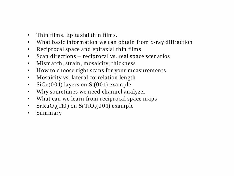
• Thin films. Epitaxial thin films.• What basic information we can obtain from x-ray diffraction• Reciprocal space and epitaxial thin films• Scan directions – reciprocal vs. real space scenarios• Mismatch, strain, mosaicity, thickness• How to choose right scans for your measurements• Mosaicity vs. lateral correlation length• SiGe(001) layers on Si(001) example• Why sometimes we need channel analyzer• What can we learn from reciprocal space maps• SrRuO3(110) on SrTiO3(001) example• Summary
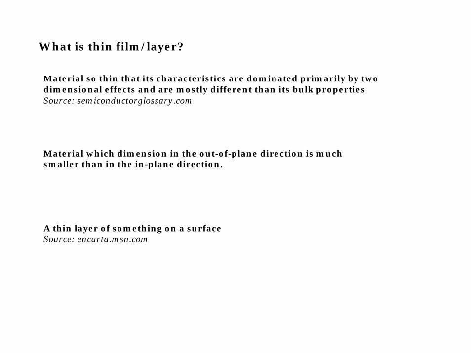
What is thin film/layer?
Material so thin that its characteristics are dominated primarily by two dimensional effects and are mostly different than its bulk propertiesSource: semiconductorglossary.com
A thin layer of something on a surfaceSource: encarta.msn.com
Material which dimension in the out-of-plane direction is much smaller than in the in-plane direction.

Epitaxial Layer
A single crystal layer that has been deposited or grown on a crystalline substrate having the same structural arrangement.Source: photonics.com
A crystalline layer of a particular orientation on top of another crystal, where the orientation is determined by the underlying crystal.
Homoepitaxial layerthe layer and substrate are the same material and possess the same lattice parameters.
Heteroepitaxial layerthe layer material is different than the substrate and usually has different lattice parameters.
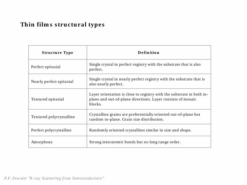
Thin films structural types
Structure Type Definition
Perfect epitaxialSingle crystal in perfect registry with the substrate that is also perfect.
Nearly perfect epitaxialSingle crystal in nearly perfect registry with the substrate that is also nearly perfect.
Textured epitaxialLayer orientation is close to registry with the substrate in both in-plane and out-of-plane directions. Layer consists of mosaic blocks.
Textured polycrystallineCrystalline grains are preferentially oriented out-of-plane but random in-plane. Grain size distribution.
Perfect polycrystalline Randomly oriented crystallites similar in size and shape.
Amorphous Strong interatomic bonds but no long range order.
P.F. Fewster “X-ray Scattering from Semiconductors”
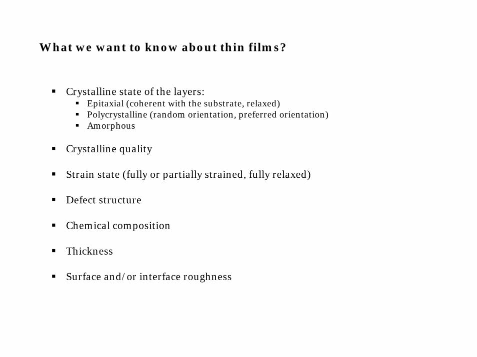
What we want to know about thin films?
Crystalline state of the layers:Epitaxial (coherent with the substrate, relaxed)Polycrystalline (random orientation, preferred orientation) Amorphous
Crystalline quality
Strain state (fully or partially strained, fully relaxed)
Defect structure
Chemical composition
Thickness
Surface and/or interface roughness
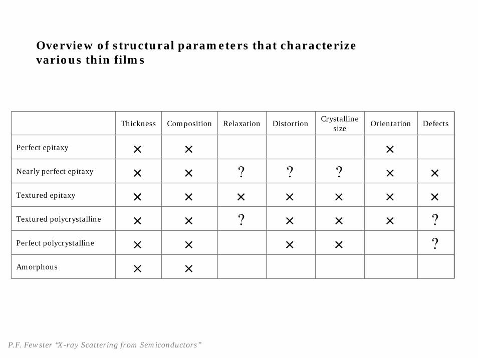
Thickness Composition Relaxation DistortionCrystalline
sizeOrientation Defects
Perfect epitaxy × × ×Nearly perfect epitaxy × × ? ? ? × ×Textured epitaxy × × × × × × ×Textured polycrystalline × × ? × × × ?Perfect polycrystalline × × × × ?Amorphous × ×
Overview of structural parameters that characterize various thin films
P.F. Fewster “X-ray Scattering from Semiconductors”
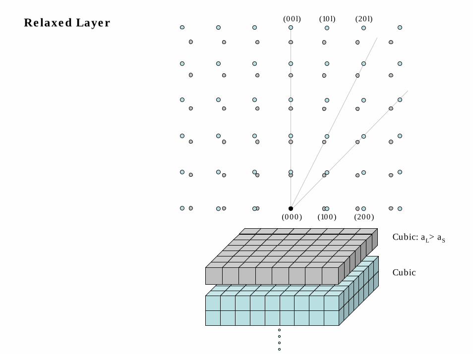
(000)
(00l)
(100) (200)
(10l) (20l)
Cubic: aL> aS
Cubic
Relaxed Layer
aL
aL aL=aS
aS
aS
cL
aS
aS
Beforedeposition
Afterdeposition
0
0
Lz
Lz
Lz
zz ddd −
==⊥ εε
Tetragonal Distortion
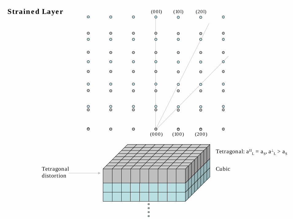
(000)
(00l)
(100) (200)
(10l) (20l)
Tetragonal: aIIL = aS, a⊥
L > aS
Cubic
Strained Layer
Tetragonaldistortion
Cubic
Cubic
Cubic
Tetragonal
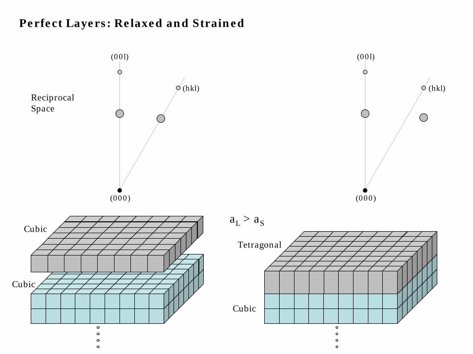
ReciprocalSpace
(000)
(00l)
(hkl)
(000)
(00l)
(hkl)
aL > aS
Perfect Layers: Relaxed and Strained
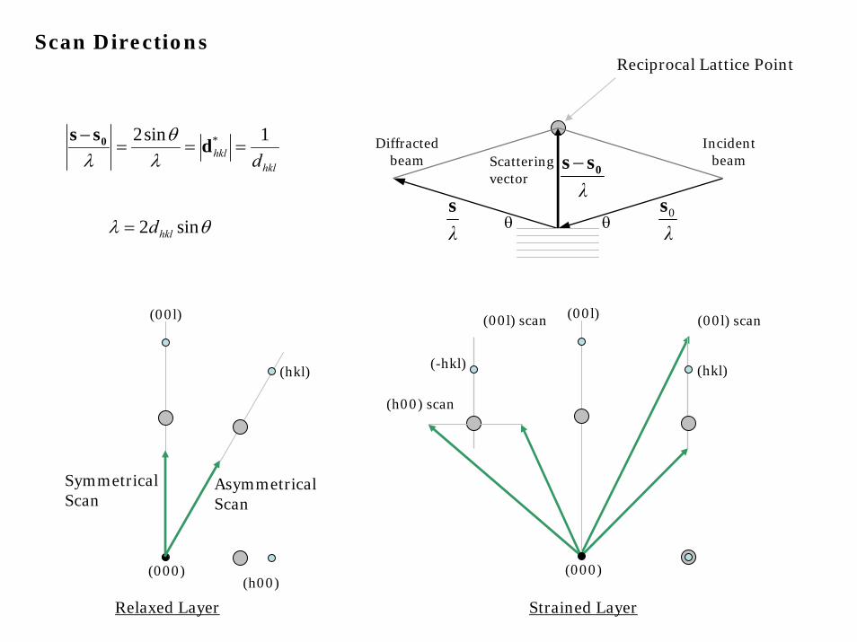
Scan Directions
Incident beam
Diffracted beam Scattering
vectorhkl
hkl d1sin2 * ===
− dss 0
λθ
λλ
0ss −
λs
λ0s
θθθλ sin2 hkld=
Reciprocal Lattice Point
(000)
(00l)
(hkl)
SymmetricalScan
AsymmetricalScan
(000)
(00l)
(hkl)
(00l) scan
(h00) scan
(h00)
(-hkl)
(00l) scan
Relaxed Layer Strained Layer
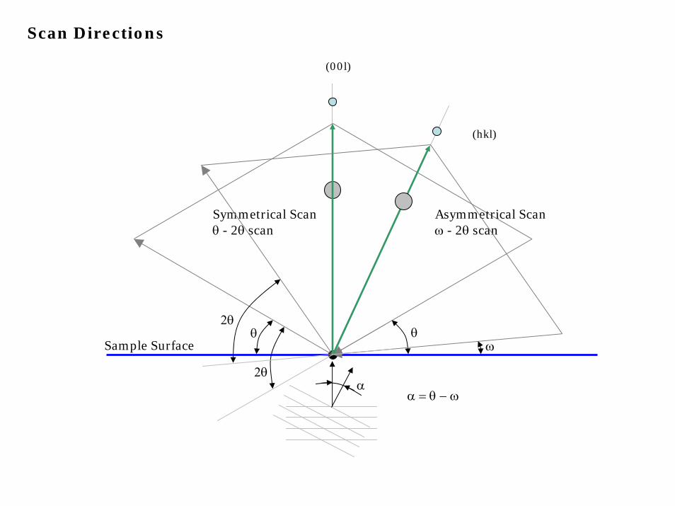
Sample Surface
(00l)
Symmetrical Scanθ - 2θ scan
θθ
2θ
(hkl)
Asymmetrical Scanω - 2θ scan
αα = θ − ω
ω
2θ
Scan Directions
Sample Surface
(00l)
(hkl)
Scan Directions
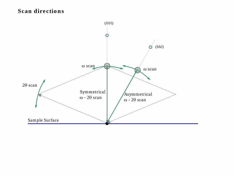
(00l)
(hkl)
Symmetricalω - 2θ scan
Asymmetricalω - 2θ scan
Sample Surface
2θ scan
Scan directions
ω scanω scan

Homoepitaxy
L
S
HeteroepitaxyTensile stress
Heteroepitaxyd-spacing variation
HeteroepitaxyMosaicity
Finite thickness effect
cL < aS
Real RLP shapes
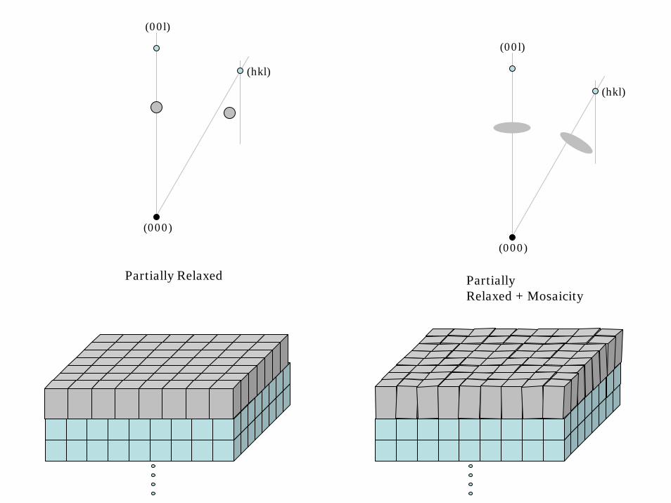
(000)
(00l)
(hkl)
PartiallyRelaxed + Mosaicity
(000)
(00l)
(hkl)
Partially Relaxed
(000)
(00l)
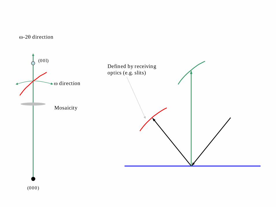
ω direction
ω-2θ direction
Defined by receiving optics (e.g. slits)
Mosaicity
(000)
(00l)
ω direction
ω-2θ direction
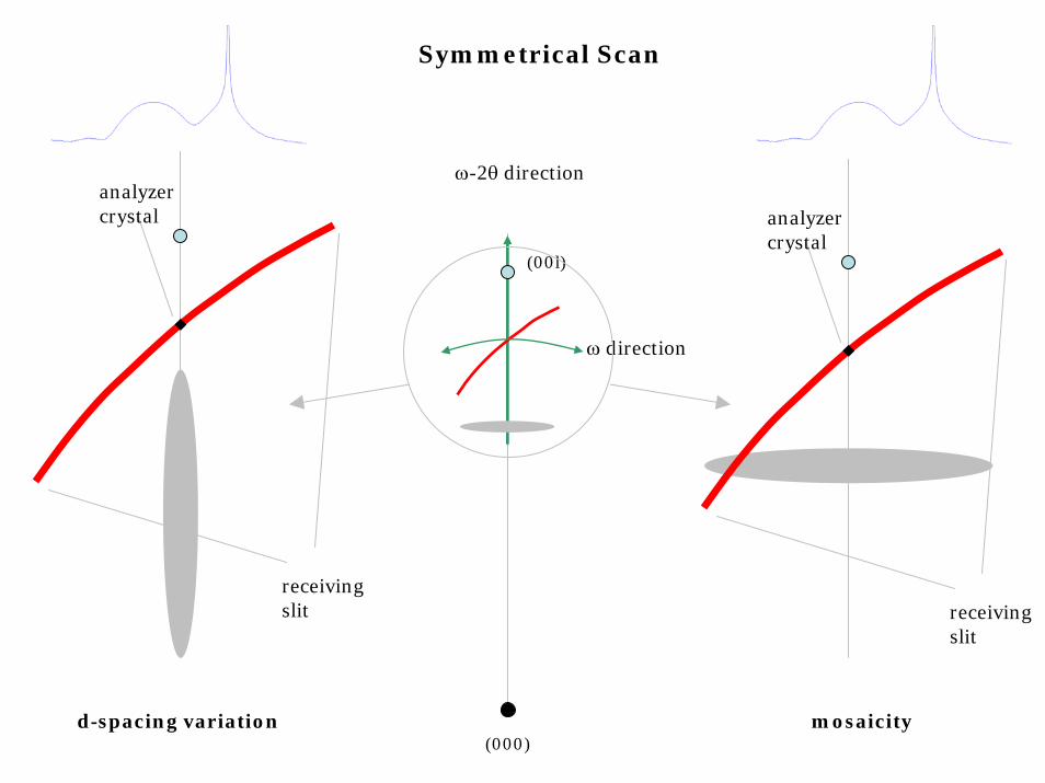
Symmetrical Scan
receivingslit
analyzercrystal
mosaicity
receivingslit
analyzercrystal
d-spacing variation
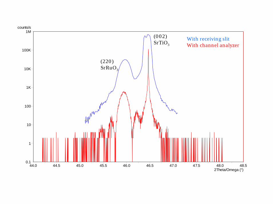
44.0 44.5 45.0 45.5 46.0 46.5 47.0 47.5 48.0 48.52Theta/Omega (°)
0.1
1
10
100
1K
10K
100K
1Mcounts/s
With receiving slitWith channel analyzer
(002)SrTiO3
(220)SrRuO3
65.5 66.0 66.5 67.0 67.5 68.0 68.5 69.0 69.5 70.0 70.52Theta/Omega (°)
0.1
1
10
100
1K
10K
100K
1M
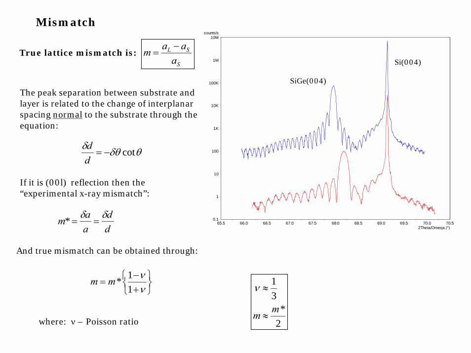
10Mcounts/s
Si(004)
SiGe(004)
The peak separation between substrate and layer is related to the change of interplanarspacing normal to the substrate through the equation:
Mismatch
θδθδ cot−=dd
If it is (00l) reflection then the “experimental x-ray mismatch”:
dd
aam δδ
==*
True lattice mismatch is:S
SL
aaam −
=
⎭⎬⎫
⎩⎨⎧
+−
=νν
11*mm
And true mismatch can be obtained through:
where: ν – Poisson ratio 2*
31
mm ≈
≈ν
6 5 .5 6 6 .0 6 6 .5 6 7 .0 6 7 .5 6 8 .0 6 8 .5 6 9 .0 6 9 .5 7 0 .02 The ta /O m e g a (°)
1 0 0
1 K
1 0 K
1 0 0 K
1 M
1 0 Mco unts /s
S
L
F
F
F
F
F
F
F
F
FF
F
F
F
F
F
F
F
F
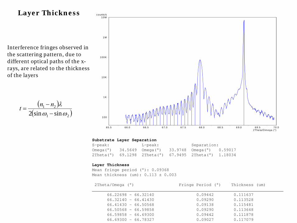
Interference fringes observed in the scattering pattern, due to different optical paths of the x-rays, are related to the thickness of the layers
( )( )
Substrate Layer SeparationS-peak: L-peak: Separation: Omega(°) 34.5649 Omega(°) 33.9748 Omega(°) 0.590172Theta(°) 69.1298 2Theta(°) 67.9495 2Theta(°) 1.18034
Layer ThicknessMean fringe period (°): 0.09368 Mean thickness (um): 0.113 ± 0.003
2Theta/Omega (°) Fringe Period (°) Thickness (um) _____________________________________________________________________________
66.22698 - 66.32140 0.09442 0.11163766.32140 - 66.41430 0.09290 0.11352866.41430 - 66.50568 0.09138 0.11548166.50568 - 66.59858 0.09290 0.11364866.59858 - 66.69300 0.09442 0.11187866.69300 - 66.78327 0.09027 0.117079
Layer Thickness
21
21
sinsin2 ωωλ
−−
=nnt
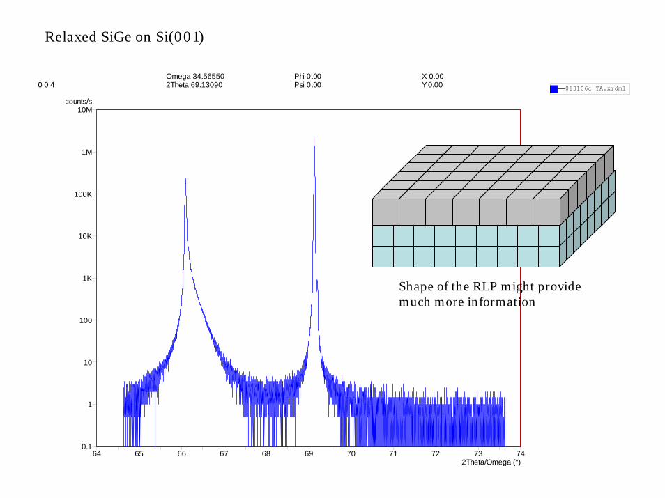
Relaxed SiGe on Si(001)
64 65 66 67 68 69 70 71 72 73 742Theta/Omega (°)
0.1
1
10
100
1K
10K
100K
1M
10Mcounts/s
0 0 4Omega 34.565502Theta 69.13090
Phi 0.00Psi 0.00
X 0.00Y 0.00 013106c_TA.xrdml
Shape of the RLP might provide much more information
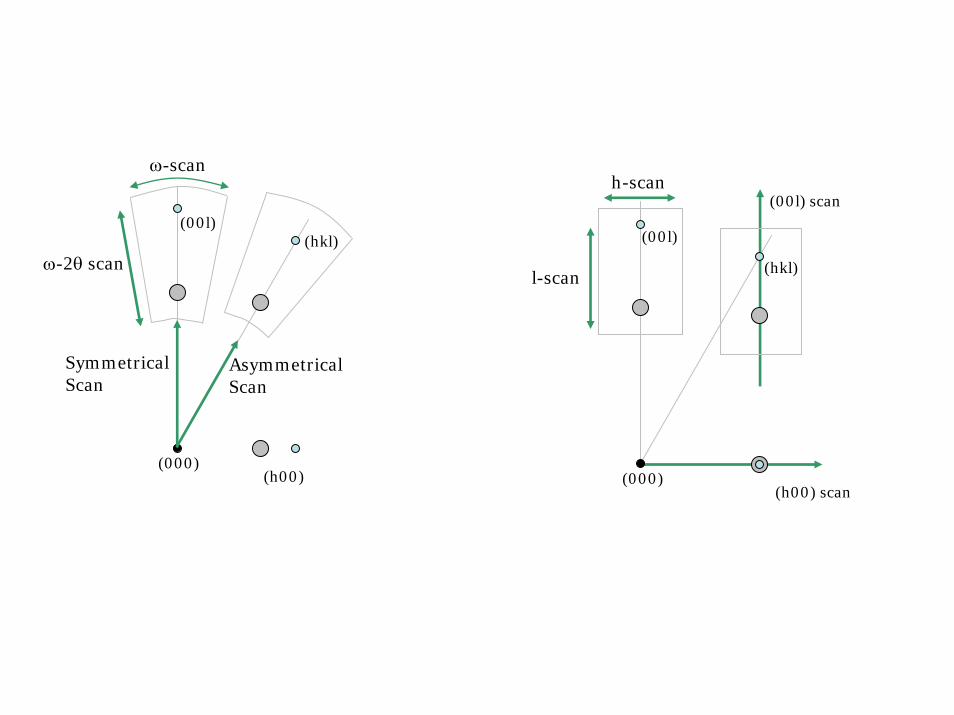
(000)
(00l)(hkl)
SymmetricalScan
AsymmetricalScan
(000)
(00l)
(hkl)
(00l) scan
(h00) scan(h00)
ω-scan
ω-2θ scan
h-scan
l-scan
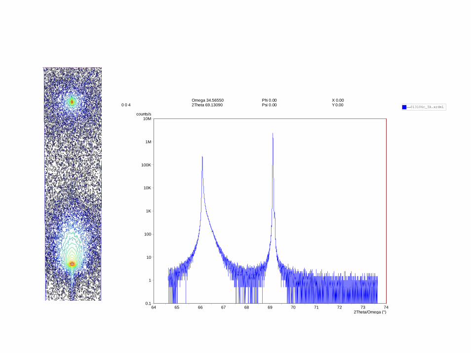
64 65 66 67 68 69 70 71 72 73 742Theta/Omega (°)
0.1
1
10
100
1K
10K
100K
1M
10Mcounts/s
0 0 4Omega 34.565502Theta 69.13090
Phi 0.00Psi 0.00
X 0.00Y 0.00 013106c_TA.xrdml

Relaxed SiGe on Si(001)
66
67
68
69
7(oo4) RLM
Si(004)
SiGe(004)
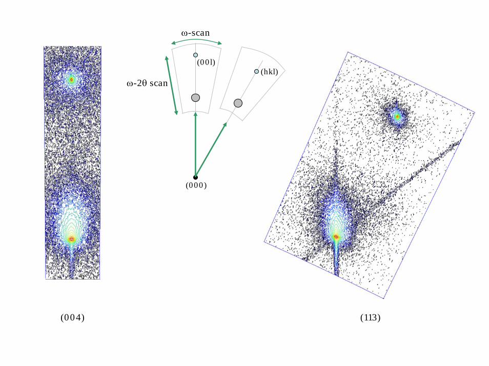
(004) (113)
(000)
(00l)(hkl)
ω-scan
ω-2θ scan

The mosaic spread of the layer is calculated from the angle thatthe layer peak subtends at the origin of reciprocal space measured perpendicular to the reflecting plane normal.
The lateral correlation length of the layer is calculated from the reciprocal of the FWHM of the peak measured parallel to the interface.
Mosaic Spread and Lateral Correlation Length
The Mosaic Spread and Lateral Correlation Length functionality derives information from the shape of a layer peak in a diffraction space map recorded using an asymmetrical reflection
LC
MS
To OriginQZ
QX
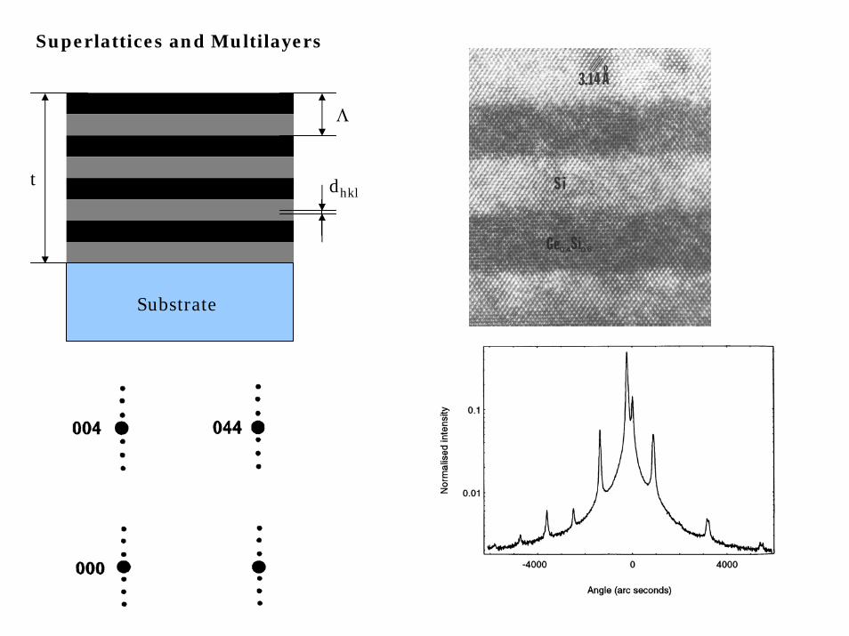
Λ
t dhkl
Superlattices and Multilayers
Substrate
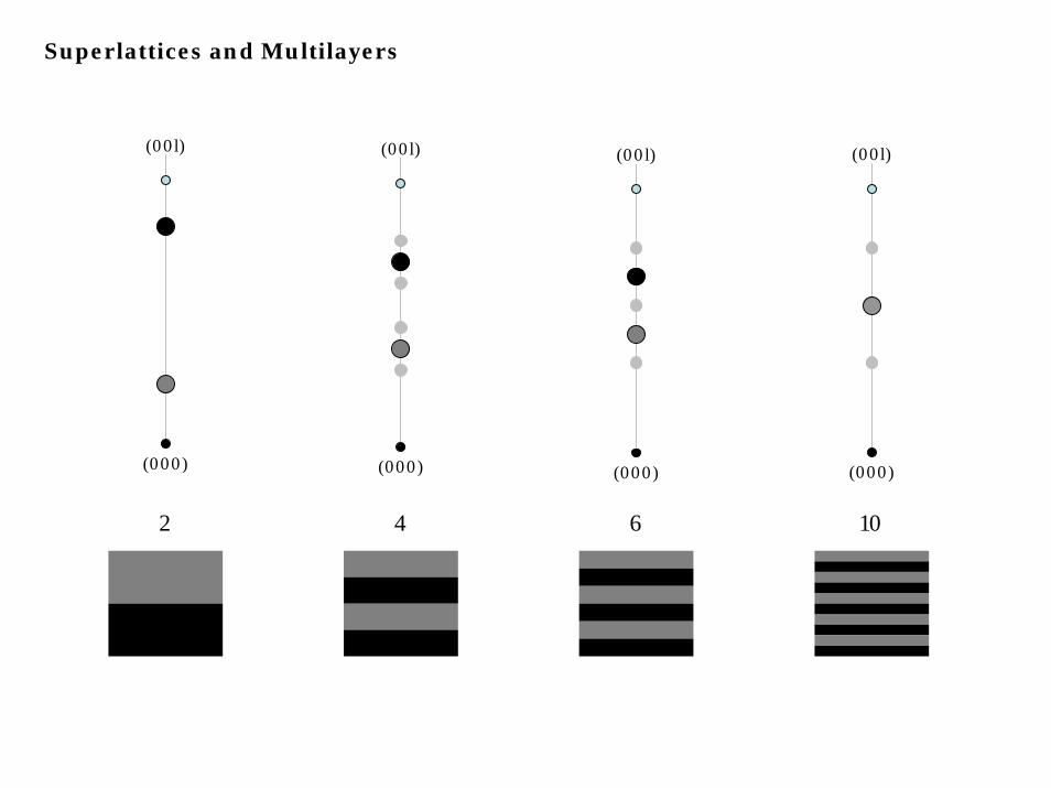
6
(000)
(00l)
10
(000)
(00l)
2
(000)
(00l)
4
(000)
(00l)
Superlattices and Multilayers
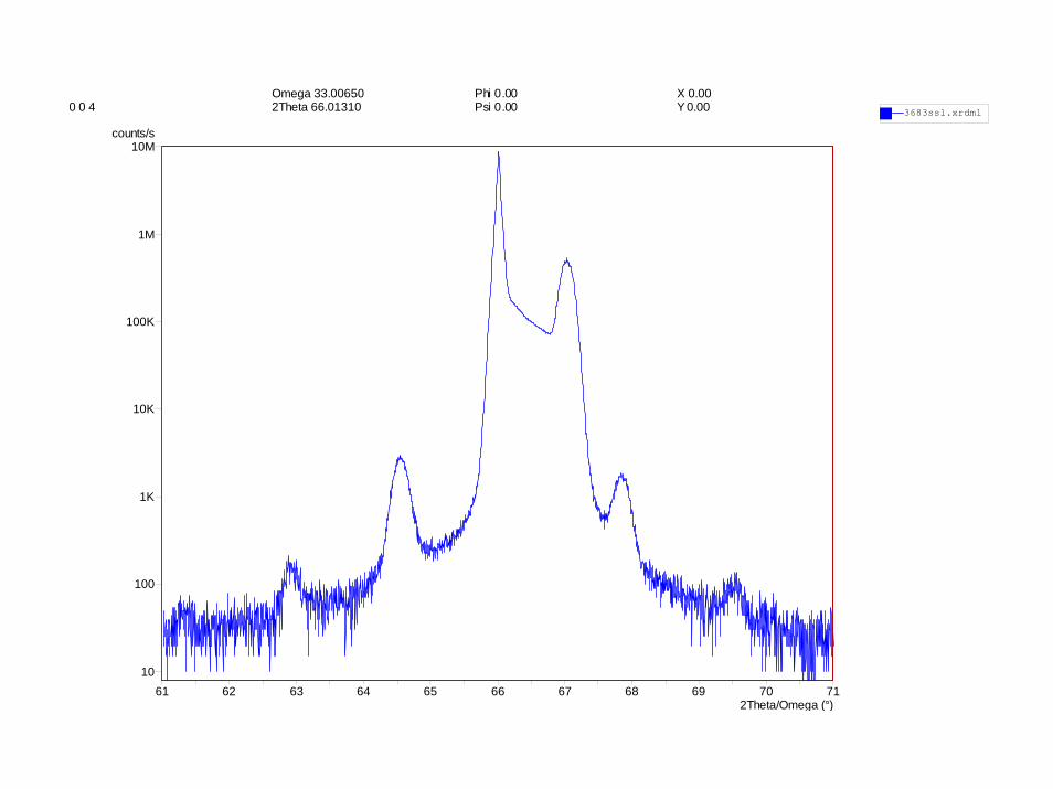
61 62 63 64 65 66 67 68 69 70 712Theta/Omega (°)
10
100
1K
10K
100K
1M
10Mcounts/s
0 0 4Omega 33.006502Theta 66.01310
Phi 0.00Psi 0.00
X 0.00Y 0.00 3683ssl.xrdml
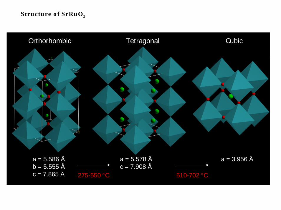
a = 5.586 Åb = 5.555 Åc = 7.865 Å
a = 5.578 Åc = 7.908 Å
a = 3.956 Å
275-550 °C 510-702 °C
Orthorhombic Tetragonal Cubic
Structure of SrRuO3
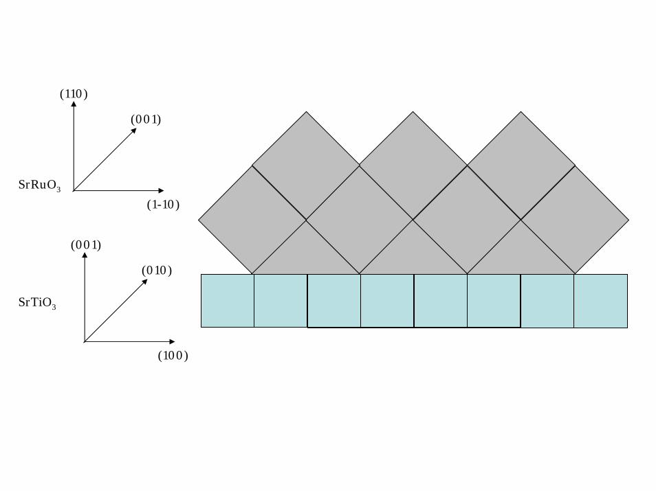
SrRuO3
SrTiO3
(110)
(001)
(1-10)
(001)
(010)
(100)
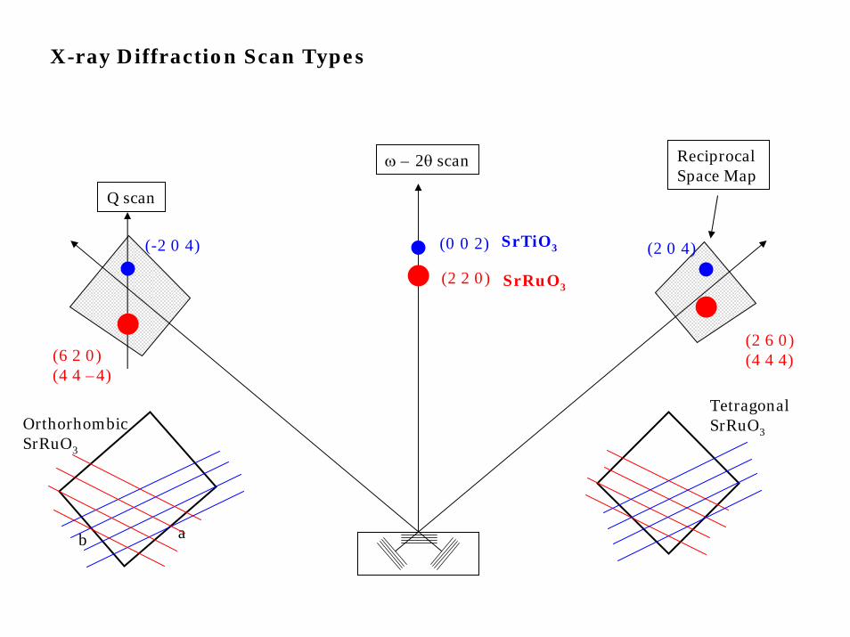
(2 6 0)(4 4 4)(6 2 0)
(4 4 –4)
(2 2 0)
(0 0 2)(-2 0 4) (2 0 4)
ω – 2θ scan Reciprocal Space Map
Q scan
SrTiO3
SrRuO3
ab
OrthorhombicSrRuO3
TetragonalSrRuO3
X-ray Diffraction Scan Types
4 5 .4 4 5 .6 4 5 .8 4 6 .0 4 6 .2 4 6 .4 4 6 .6 4 6 .8 4 7 .02 The ta /O m e g a (°)
1
1 0
1 0 0
1 K
1 0 K
1 0 0 K
co unts /s
4 5 .4 4 5 .6 4 5 .8 4 6 .0 4 6 .2 4 6 .4 4 6 .6 4 6 .82 The ta /O m e g a (°)
0 .1
1
1 0
1 0 0
1 K
1 0 K
1 0 0 K
co unts /s
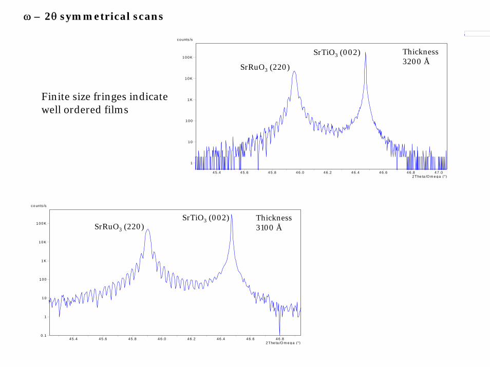
Thickness3100 Å
SrTiO3 (002)SrRuO3 (220)
SrTiO3 (002)
SrRuO3 (220)
Thickness3200 Å
Finite size fringes indicate well ordered films
ω – 2θ symmetrical scans
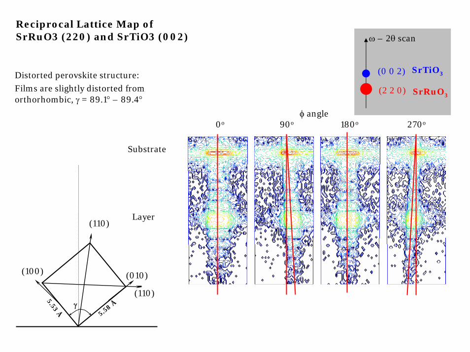
φ angle0o 90o 180o 270o
(2 2 0)
(0 0 2)
ω – 2θ scan
SrTiO3
SrRuO3
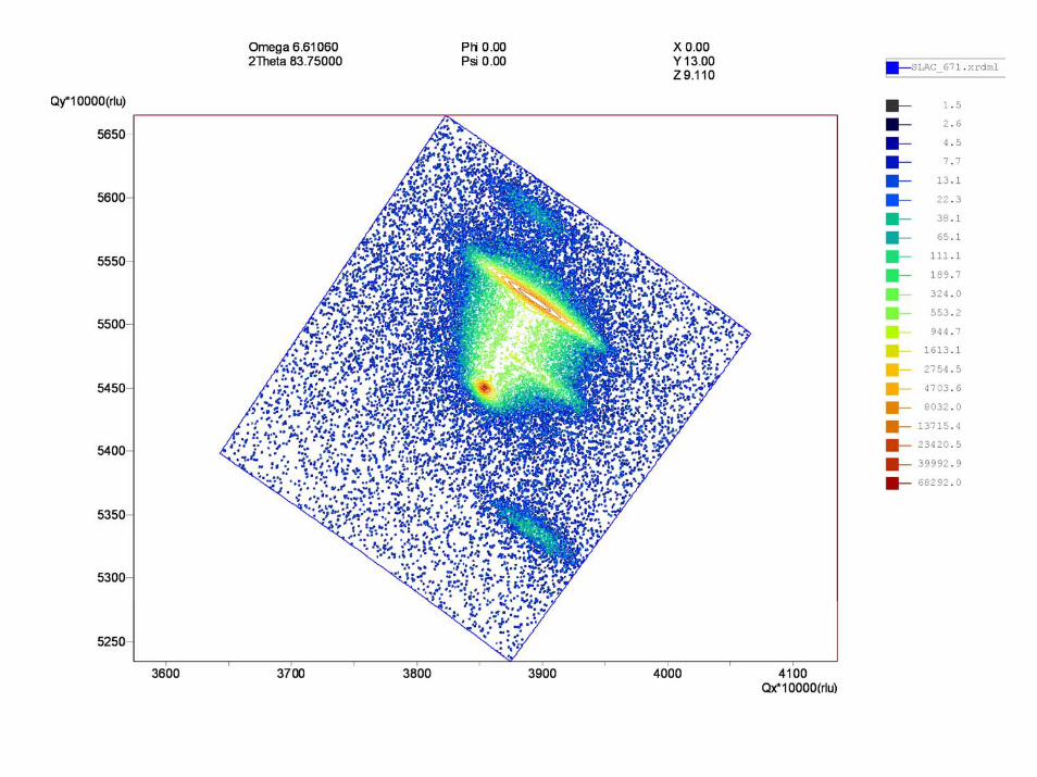
Reciprocal Lattice Map ofSrRuO3 (220) and SrTiO3 (002)
Substrate
Layer
5.53 Å 5.58 Å
Distorted perovskite structure:
Films are slightly distorted from orthorhombic, γ = 89.1° – 89.4°
γ
(110)
(110)
(100) (010)
ab
OrthorhombicSrRuO3
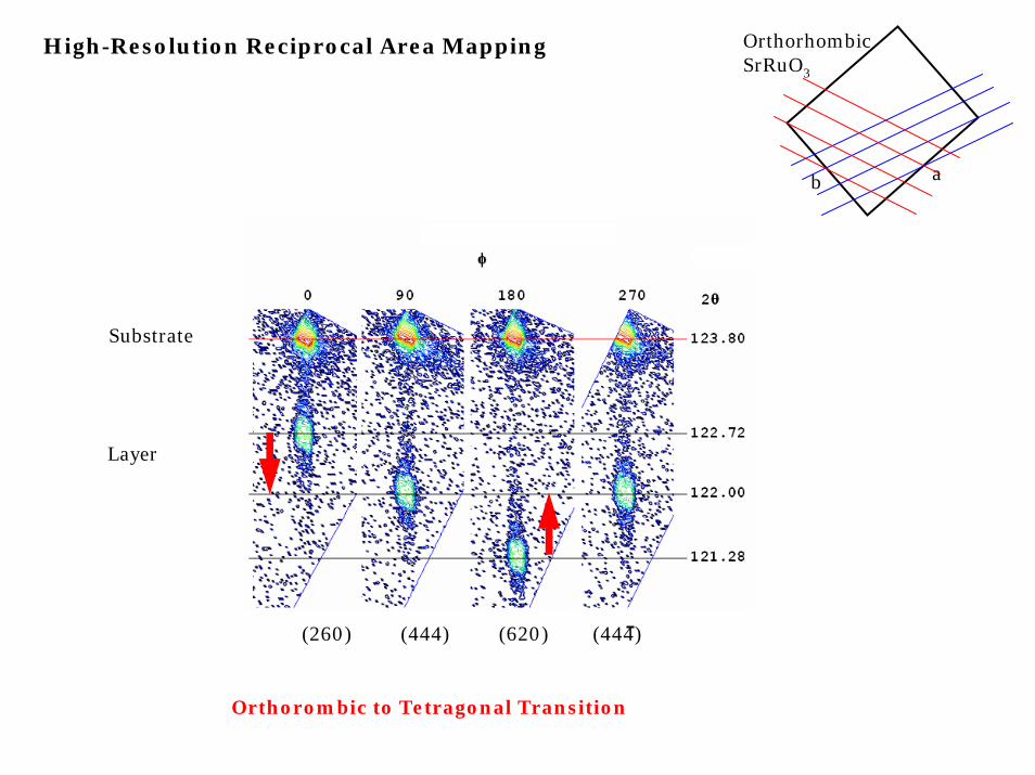
(260) (444) (620) (444)
High-Resolution Reciprocal Area Mapping
Substrate
Layer
Orthorombic to Tetragonal Transition
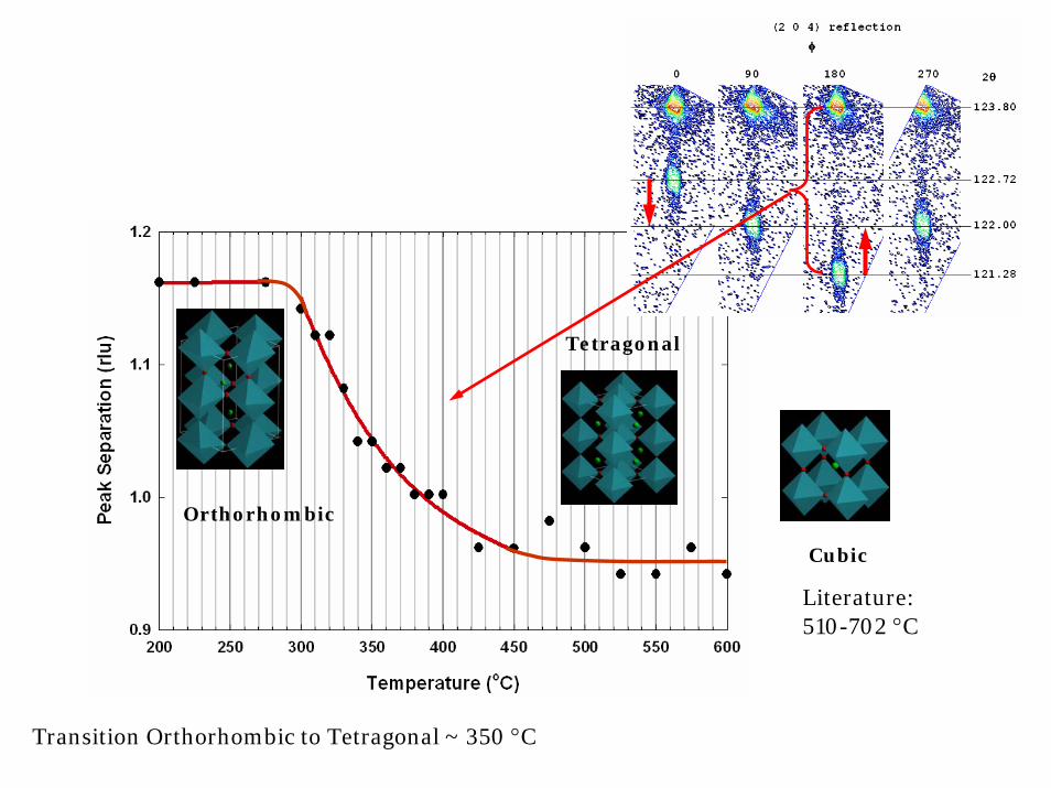
Orthorhombic
Tetragonal
Cubic
Literature: 510-702 °C
Transition Orthorhombic to Tetragonal ~ 350 °C
Temperature ( oC)
150 200 250 300 350 400
Inte
nsity
(arb
uni
ts)
0.0
0.2
0.4
0.6
0.8
1.0
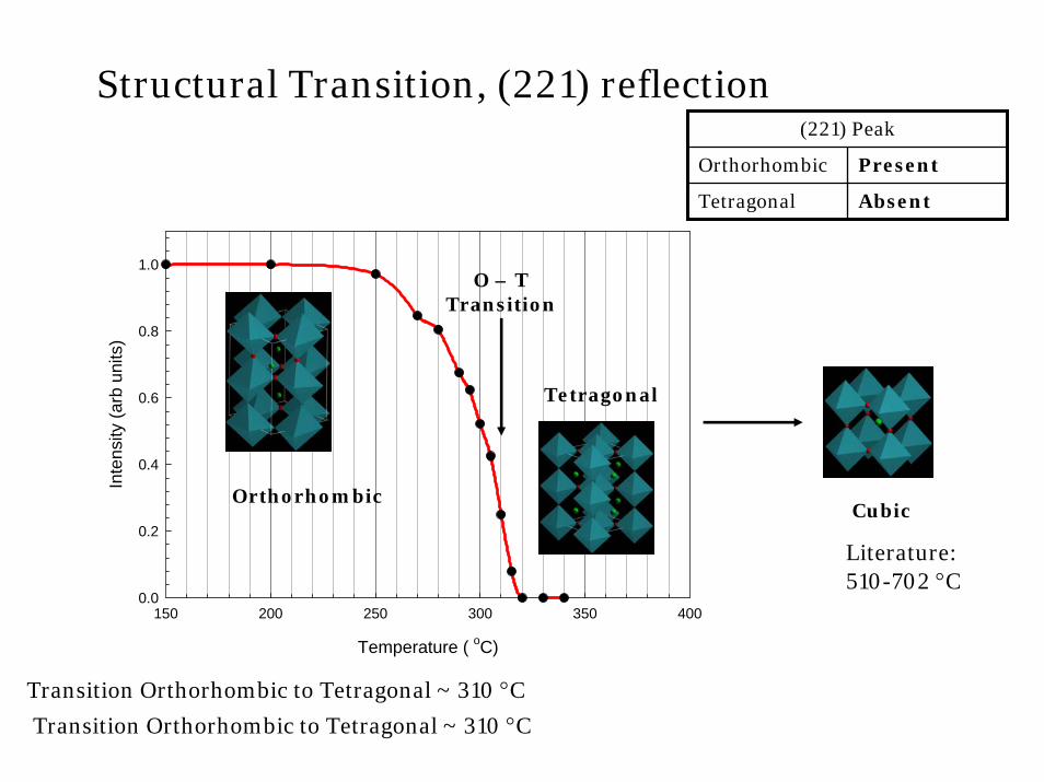
Structural Transition, (221) reflection
Orthorhombic
Tetragonal
Cubic
Literature: 510-702 °C
Transition Orthorhombic to Tetragonal ~ 310 °C
O – TTransition
(221) Peak
Orthorhombic Present
Tetragonal Absent
Transition Orthorhombic to Tetragonal ~ 310 °C

α
Rotation Angle (deg)
0 2 4 6 8 10 12 14 16
Cal
cula
ted
Inte
nsity
(arb
uni
ts)
0
10000
20000
30000
40000
50000
60000
(211) peak is absent in cubic SrRuO3
Structural Transition, (211) reflection
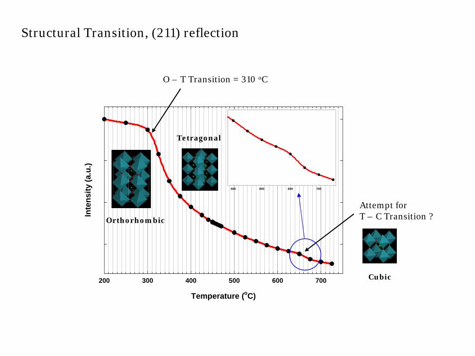
Temperature (oC)
200 300 400 500 600 700
Inte
nsity
(a.u
.)
550 600 650 700
Orthorhombic
Tetragonal
Cubic
Attempt forT – C Transition ?
O – T Transition = 310 oC
Structural Transition, (211) reflection
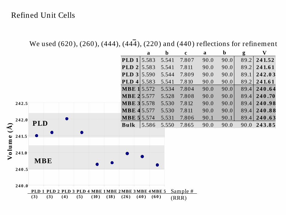
We used (620), (260), (444), (444), (220) and (440) reflections for refinement
240.0
240.5
241.0
241.5
242.0
242.5
PLD 1(3)
PLD 2(3)
PLD 3(4)
PLD 4(5)
MBE 1(10)
MBE 2(18)
MBE 3(26)
MBE 4(40)
MBE 5(60)
Vo
lum
e (
Å)
MBE
PLD
Sample #(RRR)
a b c a b g VPLD 1 5.583 5.541 7.807 90.0 90.0 89.2 241.52PLD 2 5.583 5.541 7.811 90.0 90.0 89.2 241.61PLD 3 5.590 5.544 7.809 90.0 90.0 89.1 242.03PLD 4 5.583 5.541 7.810 90.0 90.0 89.2 241.61MBE 1 5.572 5.534 7.804 90.0 90.0 89.4 240.64MBE 2 5.577 5.528 7.808 90.0 90.0 89.4 240.70MBE 3 5.578 5.530 7.812 90.0 90.0 89.4 240.98MBE 4 5.577 5.530 7.811 90.0 90.0 89.4 240.88MBE 5 5.574 5.531 7.806 90.1 90.1 89.4 240.63Bulk 5.586 5.550 7.865 90.0 90.0 90.0 243.85
Refined Unit Cells
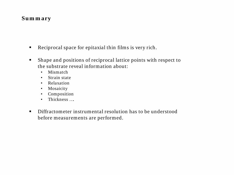
Summary
Reciprocal space for epitaxial thin films is very rich.
Shape and positions of reciprocal lattice points with respect tothe substrate reveal information about:
• Mismatch• Strain state• Relaxation• Mosaicity• Composition• Thickness ….
Diffractometer instrumental resolution has to be understood before measurements are performed.
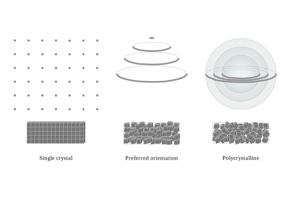
PolycrystallinePreferred orientationSingle crystal