Embed Size (px)
Citation preview

Thin Films and Diffusion


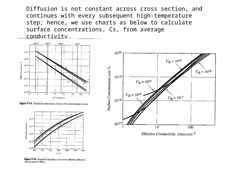
Diffusion is not constant across cross section, and continues with every subsequent high-temperature step; hence, we use charts as below to calculate surface concentrations, Cs, from average conductivity,
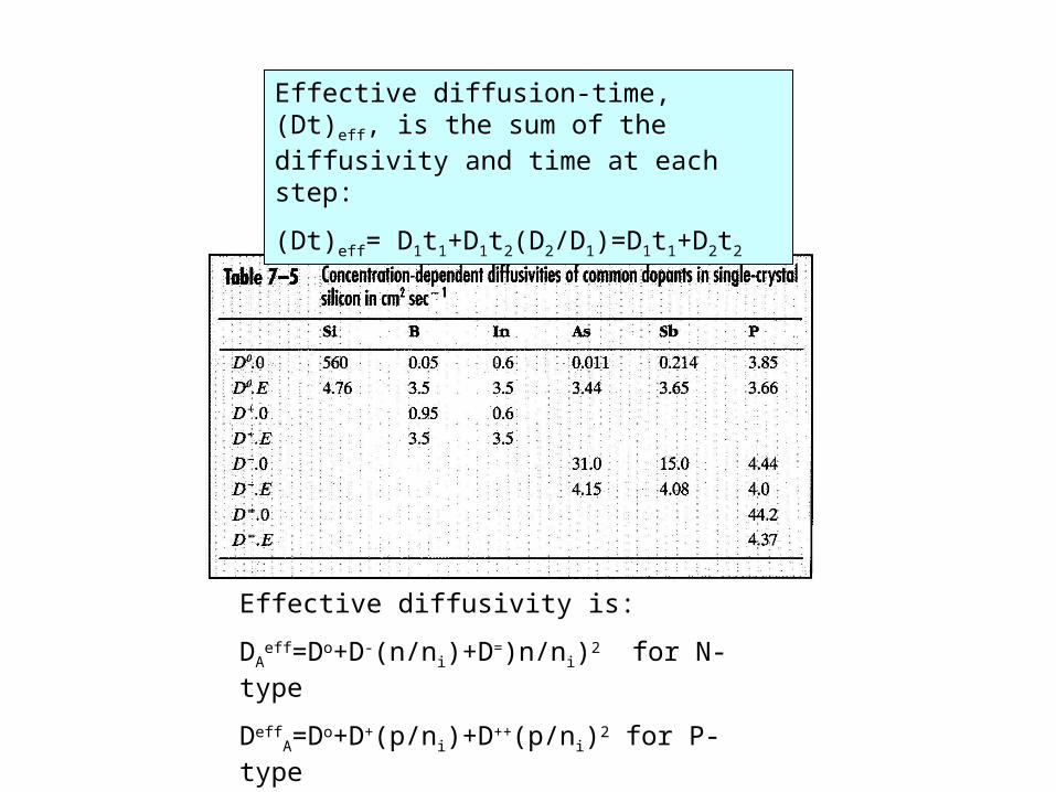
Effective diffusivity is:
DAeff=Do+D-(n/ni)+D=)n/ni)2 for N-type
DeffA=Do+D+(p/ni)+D++(p/ni)2 for P-type
Values are tabulated, as in table 7.5
Effective diffusion-time, (Dt)eff, is the sum of the diffusivity and time at each step:
(Dt)eff= D1t1+D1t2(D2/D1)=D1t1+D2t2

Diffusion Data

Example
Figure 7-17 Dopant surface concentration vs. effective conductivity for various substrate concentrations, CB

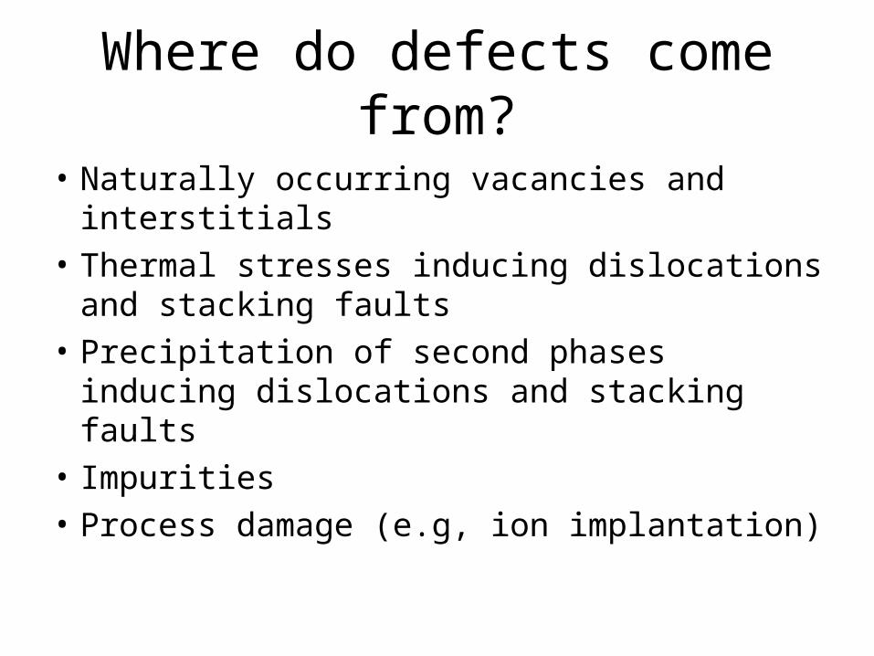
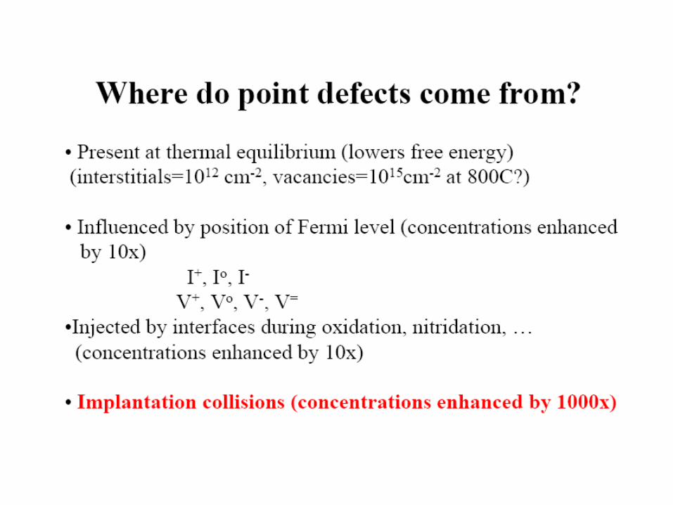
Where do defects come from?
• Naturally occurring vacancies and interstitials
• Thermal stresses inducing dislocations and stacking faults
• Precipitation of second phases inducing dislocations and stacking faults
• Impurities
• Process damage (e.g, ion implantation)

Precipitates and Dislocations
Precipitates usually do not fit into the host lattice. The growing particle causes considerable stress that can be reduced by plastic deformation.
If the precipitate fits in one lattice direction, but not in others (a precipitate with an hexagonal lattice, e.g., may fit relatively well on the {111} planes of an fcc lattice) a compromise between a non-spherical shape of the precipitate and a system of dislocation loops in some direction may produce least strain energy. The precipitate-dislocation system then has a very specific structure; the process is known as "prismatic loop punching". An example is shown below on the left (taken under kinematic bright field conditions).
Precipitate with prismatic loops. An arrangement like that accounts for the peculiar etch features shown before
Plate-like precipitate (the dark grey feature) with dislocations relieving parts of the stress.

The oval shaped area with a lighter contrast is the emitter of a bipolar transistor. In preferential etching this would look similar to what was shown as an illustration for etching.
Some of these small stacking faults have a peculiar, "sailing-boat" like shape (marked by "S" in the picture above). Below, a detailed view of a "sailing boat stacking fault":
• Oxidation of Silicon produces interstitials in supersaturation. These surplus interstitials tend to agglomerate in discs - i.e. stacking fault loops. The difficult part is the nucleation; it determines what will happen. We have to consider two ways of oxidizing Si, we first consider Surface oxidation: The surface oxidizes homogeneously by exposing it to an oxidizing atmosphere at high temperatures. This is the normal oxidation process. The emission of interstitials occurs at the interface; the interstitials diffuse into the bulk; the supersaturation decreases with the distance from the surface. There is no easy nucleation for an interstitial type dislocation loop as long as the interface is defect free. If defects are present, most prominent small precipitates of metal impurities (Fe, Ni, Cu) may serve as nucleation centers for the interstitials; a stacking fault penetrating in a semicircular fashion into the bulk is formed. If many precipitates are available, a large density of small stacking faults may be observed:

The name "swirl" comes from the spiral "swirl-like" pattern observed in many cases by preferential etching as shown on the right.Close inspection revealed two types of etch features which must have been caused by different kinds of defects. Lacking any information about the precise nature of the defects (which etching can not give), they were termed "A-" and "B-swirl defects".

Looking at the etch pattern with a microscope at high magnifications shows that there are a lot of small defects (the B-swirls; white dots) and a much smaller number of larger defects (A-swirls; the black-white contrasts). Quantitative evaluation of the micrograph shows that the B-swirls are delineated as small and shallow pits whereas the A-swirls are delineated as hillocks.
Swirl defects are generated by the agglomeration of point defects while the crystals cools. The Si crystal growing industry soon learned how to grow crystals without swirl defects - without ever understanding precisely what they were.
But that did not mean that the crystals were defect free - it only meant that the methods


![Nanosizing Ammonia Borane with Nickel: A Path toward … of Materials Science and Engineering and Integrated Materials ... mass transfer and hydrogen diffusion.[35] Hence, confinement](https://img.pdfslide.net/doc/110x75/5aae14e67f8b9a5d0a8bab33/nanosizing-ammonia-borane-with-nickel-a-path-toward-of-materials-science-and.jpg)