Embed Size (px)
Citation preview
Accepted by Thin Solid Films
Strategies to Control the Spectral Properties of Au-Ni Thin Films
David J McPhersona, Supitcha Supansomboona, Benjamin Zwanb, Vicki J Keastb, David L Cortiec,d, Angus
Gentlea, Annette Dowda and Michael B Cortiea*
aInstitute for Nanoscale Technology, University of Technology Sydney, PO Box 123, Broadway NSW 2007, Australia
bSchool of Mathematical and Physical Sciences, University of Newcastle, Callaghan NSW 2308, Australia
cInstitute for Superconducting and Electronic Materials, University of Wollongong, Wollongong, NSW 2522, Australia
dAustralian Nuclear Science and Technology Organisation, Lucas Heights, NSW 2234, Australia
*Corresponding author: Tel.: +61 2 9514 2208
E-mail address: [email protected]
Keywords: physical vapor deposition, optical properties, multilayers, ab initio calculation, gold-nickel
ABSTRACT
Gold and nickel have quite different dielectric functions. Here we use a combination of calculation and
sample manufacture to assess two strategies by which thin films of these elements can be produced with a
controlled range of far-field optical properties. In the first approach, control can be achieved by
manipulating the density of states of metastable solid solutions, which in turn controls the dielectric
function. In the second approach the optical properties of the films is controlled by varying the geometry of
stacks fabricated from the constituent elements. We show that the two approaches can produce equivalent
results so both are viable options in practice. Modeling is used to reveal how the structure controls the
optical properties and to map out the possible color gamut. Predictions are tested with thin film samples
fabricated by magnetron sputtering. 1
Accepted by Thin Solid Films1. Introduction
The yellow color of bulk gold is the consequence of the element's unusual dielectric function . Specifically,
there is a well-defined band edge at about 2.4 eV (equivalent to green light, at a vacuum wavelength of
about 515 nm). This band edge corresponds to the minimum photon energy capable of exciting electronic
interband transitions from occupied to unoccupied states. Impinging photons of greater energy (i.e. shorter
wavelength) are readily absorbed by the metal whereas photons of lesser energy will normally be scattered
(reflected). Therefore, the reflectance of Au surfaces rises sharply as the wavelength of light is increased
beyond the band edge. This results in the surface reflecting red, orange and yellow colors much more
strongly than the blue to green colors, giving gold its characteristic color. In contrast, the band edge of Ag
and most other metals lies in the UV, and hence they appear colorless (silver) to the human eye.
Here we analyze and compare two different microstructural strategies by which Ni can be used to
modify the spectral properties of thin films of Au. The strategies are generic and, in principle, certain other
elements, such as Fe, could be substituted for the Ni.
In the first approach we modify the electronic density-of-states (DOS) of the Au by adding Ni as an
alloying element. This 'bleaches' (whitens) the color by modifying the location of the band edge and strength
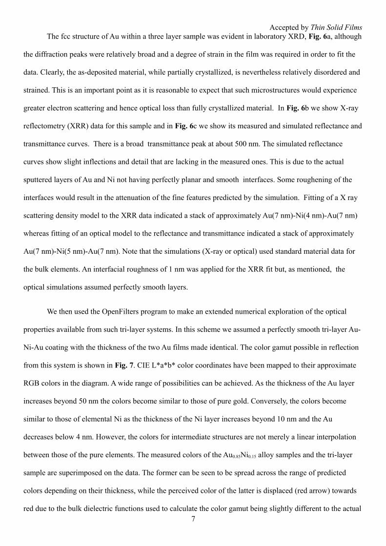
of the interband transitions . Actually, while mutually soluble above 810 °C, the equilibrium solubility of Ni
in Au, and vice versa, is negligible at room temperature because the binary phase diagram is characterized
by a complete miscibility gap at room temperature , Fig.1. Therefore, at first sight, bleaching of thin films of
Au by modification of its band structure with Ni should not be possible at room temperature. Nevertheless,
bleaching by this means is still feasible because metastable solutions of Ni in Au can be prepared, for
example by annealing an alloy sample above 1000 K and then quenching it to room temperature, or by co-
depositing Ni and Au onto a cold substrate using physical vapor deposition.
There have been only a few studies on the optical properties of such metastable Au-Ni alloys or on
those of the somewhat analogous Au-Fe system . In general, the presence of transition metal impurities such
as Ni are expected to generate a virtual bound state (VBS) within the conduction band of the Au with the
width of the VBS increasing as the impurity content increased . This would cause enhanced scattering of
Accepted by Thin Solid Filmsconduction band electrons, i.e. a reduction in electrical conductivity, particularly at energies below the band
edge . This is usually correlated with an increase in optical 'loss' and decreased reflectance. However,
addition of Ni to Au concurrently causes a reduction of the interband absorption at energies above the band
edge, in proportion to the quantity of Ni added . The net result of these two opposing tendencies is that the
reflectance at wavelengths above the band edge (i.e. towards the infrared) is reduced (due to the reduction in
conductivity) whilst the reflectance at wavelengths below the band edge (ie. towards the ultraviolet) is
increased . The overall effect is to de-saturate the color and, in the CIE L*a*b* color system, attenuate the
luminance (brightness) of the alloy's surface.
The second approach to controlling the spectral properties exploits the immiscibility of Au and Ni at
room temperature. In this case the far-field spectral properties are derived from a nanoscale mixture of the
pure elements. Provided the size scale of the nanostructure is well below the incident wavelength, light can
penetrate through it and interact with buried features. The result is that the far-field optical properties of the
alloy are a hybrid combination of those of the individual phases. In a sense, the heterogeneous
microstructure may be thought of as a meta-material whose effective dielectric properties are determined by
the volume fraction and morphology of the Au and Ni regions and, possibly, by the amount of Ni remaining
in the metastable solid solution of the Au-rich phase, and vice versa.
2. Methodology Section
2.1 Calculations using Density Functional Theory
In this study, calculations of the DOS for a number of different nickel concentrations were made using
WIEN2k, an all-electron, linear augmented plane-wave density functional theory (DFT) code . The complex
dielectric function, =1+i2, was calculated using the OPTIC routine within WIEN2k. These calculations are
based on the random phase approximation and neglect local field effects . The dielectric function was then
used to obtain a theoretical reflectivity spectrum. The structures were generated by replacing atoms in the
gold fcc structure with increasing numbers of Ni atoms. Note that WIEN2k does not simulate a random solid
3
Accepted by Thin Solid Filmssolution, and the Ni atoms in our simulations are on a periodic lattice. However, different configurations of
Ni atoms were tested for Au0.875Ni0.125 and the effect on the optical response was found to be negligible.
Similarly, relaxation of the lattice parameter of this alloy gave values to within 1% of that of pure Au and
had a negligible effect on the optical response.
2.2 Optical property calculations
The properties of thin film stacks were modeled using OpenFilters . This freely-available software calculates
the optical properties of a stack of thin films using analytical expressions derived using the characteristic
matrix approach. Colors are estimated by applying the CIE color space model, a standard illuminant (CIE-
D65 white light) and a standardized observer (CIE-1964) to the calculated reflectance spectra. The published
dielectric functions of bulk, annealed gold and nickel were used . The simulations included 1 mm of fused
SiO2 glass as a substrate.
2.3 Preparation of thin films
The experimental samples for our study were deposited onto clear glass slides (Knittel Glaser). These had
been cleaned by sonication in a sequence of acetone, ethanol and then water for 10 minutes at each step,
rinsed with ultrapure water and immediately dried with N2. Film fabrication was carried out using dual
magnetron sputtering from Au and Ni targets of 50 mm diameter using independent control of electrical
power (typically 62 W for the Au, with the power on the Ni target varied between 26 and 60 W). Deposition
rates were calibrated using a quartz crystal sensor and were of the order of 0.1 to 0.3 nm.s-1 for the alloy. The
substrate was at room temperature, the base pressure was about 1.3x10⁻⁴ Pa and the operating pressure in the
chamber in the range 0.24 to 0.28 Pa of Ar. A rotating stage was used to provide a uniform coverage. In the
case of multilayer samples, the first and last layers were Au, with the Au top layer intended to prevent
oxidation of the Ni intermediate layer.
Accepted by Thin Solid Films
2.4 Characterization of thin films
Glancing angle X ray diffraction (XRD) and X ray reflectometry (XRR) was carried out on a PANanalytical
X'Pert PRO diffractometer with a Cu-K source (0.15418 nm) in the standard Bragg-Brentano geometry.
The accelerating voltage in both cases was 40 kV and the tube current 40 mA. The time per step was 5 s.
For the XRD the step size was 0.05° and the angle of incidence () was 1°. For the XRR the step size was
0.005°. In both cases the beams were collimated and filtered.
Reflection and transmission spectra of the thin films were acquired using a Perkin Elmer 950
Lambda UV/Vis/NIR at an angle of incidence of 8° and a Varian Cary 5E UV/Vis/NIR at incident angle of
0°, respectively. Estimates of the dielectric function of the alloy samples were extracted with WVASE32
(product of J A Woollam Co., Inc. of Lincoln, NE 68508, USA). The optical constants were obtained by
fitting Lorentz oscillator models to the transmission and reflection spectra, which ensured the Kramers-
Kronig consistency.
3. Results and Discussion
3.1. Metastable (Au,Ni) alloys
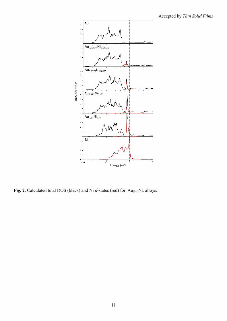
Fig. 2 shows the total electronic DOS and the partial DOS for the Ni d-states for each alloy modeled.
The DOS for pure gold is dominated by the d-band and the appearance of the transition metal dopant states
(of Ni) as a VBS just below the Fermi level is clearly observed. The data are in qualitative agreement with
the experimental valence band spectra for Au(1-x)Nix and with much earlier calculations .
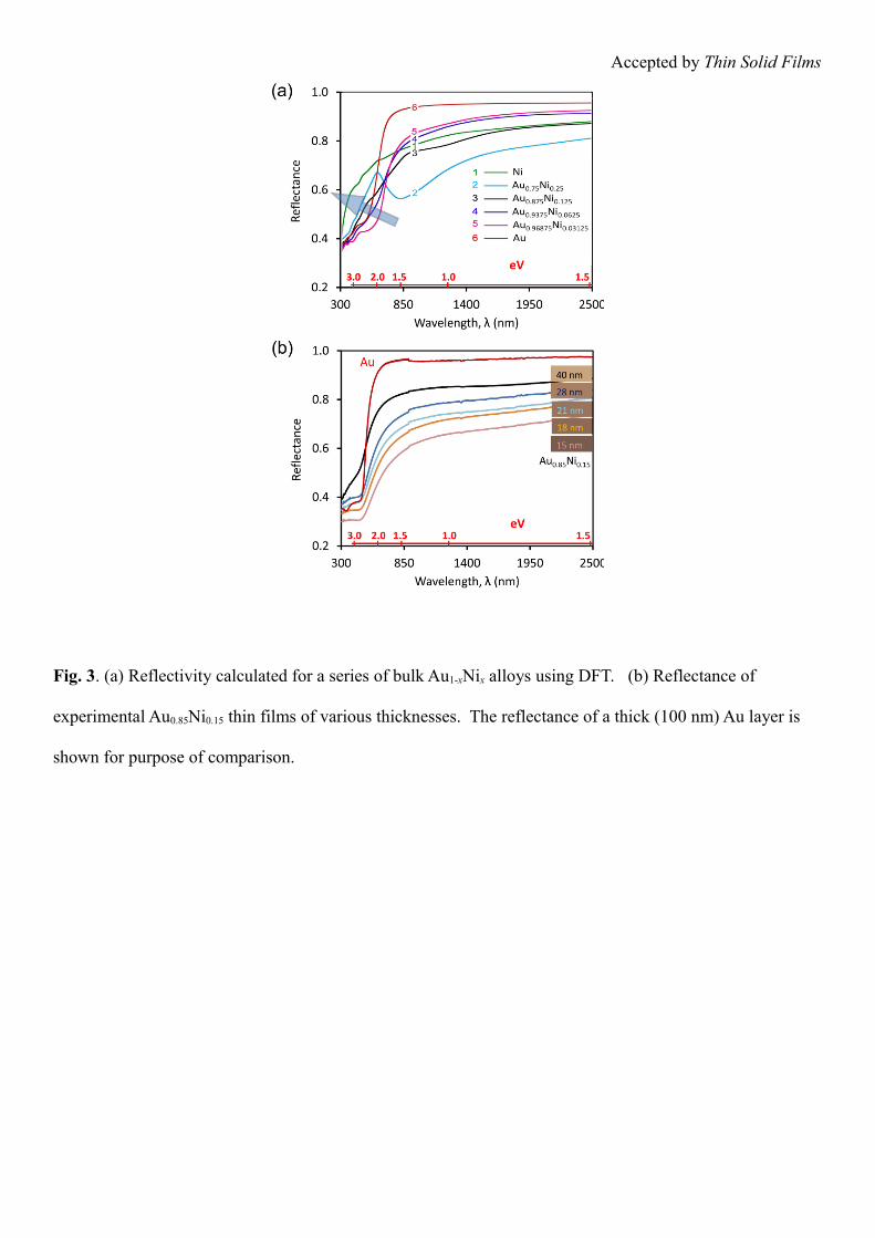
The theoretical reflectivity spectra of Fig. 3a show that, as the nickel concentration increases, the
reflectivity at long wavelengths should be attenuated relative to that of pure gold and the absorption edge
should shift to shorter wavelengths (arrow). The calculated reflectivity of the Au0.875Ni0.125 compares very
favorably to the measured reflectivity of a range of actual Au0.85Ni0.15 samples of different thickness, 5
Accepted by Thin Solid Filmsespecially when referenced to pure Au, as shown in Fig. 3b. The changes in reflectivity can be attributed to
the additional interband transitions from the VBS. At lower concentrations of Ni the theoretical reflectivity
is intermediate in shape but the trend is not exactly monotonic indicating that precise details of the interband
transitions are probably important. Once the alloy concentration increases to 25 at% the Ni states appear to
introduce an additional free-electron like contribution to the reflectivity and it evolves towards the
reflectivity of pure Ni. At wavelengths shorter than the band edge, Au0.875Ni0.125 and Au0.75Ni0.25 have a
reflectance greater than that of pure Au, i.e. their interband transitions have been attenuated. This is
consistent with the decrease in the Au d-band DOS. In contrast the 3.125at% Ni alloy has less reflectance in
this region i.e. it has stronger interband transitions than pure Au. However, overall pure Au has a greater
differential in reflectivity above and below the band edge and hence a stronger color. Reduction of this
differential is hence associated with bleaching of the color.
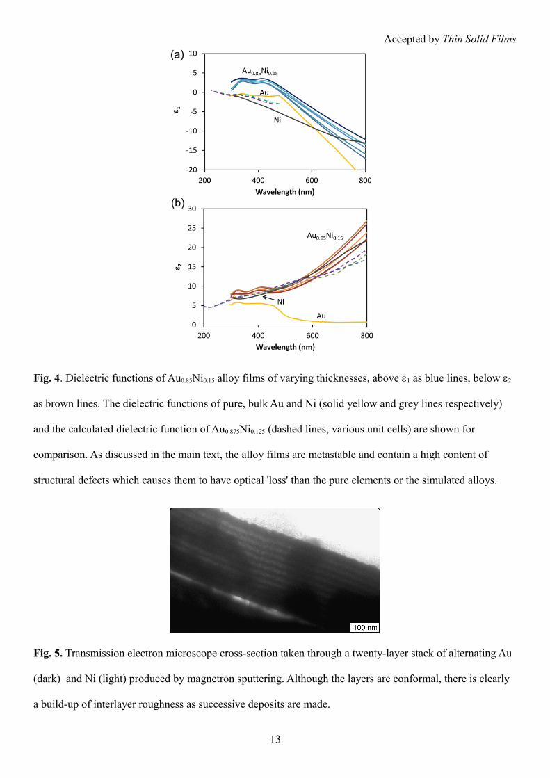
Variation of the thickness of films of fixed stoichiometry provides another way to control spectral
properties. The experimental Au0.85Ni0.15 films became more reflective (and whiter) as they became thicker.
This is because less light was lost by transmittance through the thicker coatings. Despite this variation in
reflectance, the dielectric functions of these experimental alloy films were tightly clustered, Fig.4,
indicating that the extracted values were a true material property. However, it is clear that the alloy films
would exhibit greater optical 'loss' than either the pure elements Au and Ni, or the computed metastable
alloys.
3.2 Thin film stacks of the elements
The other route to controlling the spectral-selectivity of the reflectance is to lay down separate
multilayers of Au and Ni. In principle many alternating layers can be deposited but in practice the roughness
of the interlayer interfaces increases with each additional layer, Fig. 5. This complicates analysis using
standard thin film software. Therefore, in the present paper we restrict our detailed analysis to tri-layer
stacks.
Accepted by Thin Solid Films The fcc structure of Au within a three layer sample was evident in laboratory XRD, Fig. 6a, although
the diffraction peaks were relatively broad and a degree of strain in the film was required in order to fit the
data. Clearly, the as-deposited material, while partially crystallized, is nevertheless relatively disordered and
strained. This is an important point as it is reasonable to expect that such microstructures would experience
greater electron scattering and hence optical loss than fully crystallized material. In Fig. 6b we show X-ray
reflectometry (XRR) data for this sample and in Fig. 6c we show its measured and simulated reflectance and
transmittance curves. There is a broad transmittance peak at about 500 nm. The simulated reflectance
curves show slight inflections and detail that are lacking in the measured ones. This is due to the actual
sputtered layers of Au and Ni not having perfectly planar and smooth interfaces. Some roughening of the
interfaces would result in the attenuation of the fine features predicted by the simulation. Fitting of a X ray
scattering density model to the XRR data indicated a stack of approximately Au(7 nm)-Ni(4 nm)-Au(7 nm)
whereas fitting of an optical model to the reflectance and transmittance indicated a stack of approximately
Au(7 nm)-Ni(5 nm)-Au(7 nm). Note that the simulations (X-ray or optical) used standard material data for
the bulk elements. An interfacial roughness of 1 nm was applied for the XRR fit but, as mentioned, the
optical simulations assumed perfectly smooth layers.
We then used the OpenFilters program to make an extended numerical exploration of the optical
properties available from such tri-layer systems. In this scheme we assumed a perfectly smooth tri-layer Au-
Ni-Au coating with the thickness of the two Au films made identical. The color gamut possible in reflection
from this system is shown in Fig. 7. CIE L*a*b* color coordinates have been mapped to their approximate
RGB colors in the diagram. A wide range of possibilities can be achieved. As the thickness of the Au layer
increases beyond 50 nm the colors become similar to those of pure gold. Conversely, the colors become
similar to those of elemental Ni as the thickness of the Ni layer increases beyond 10 nm and the Au
decreases below 4 nm. However, the colors for intermediate structures are not merely a linear interpolation
between those of the pure elements. The measured colors of the Au0.85Ni0.15 alloy samples and the tri-layer
sample are superimposed on the data. The former can be seen to be spread across the range of predicted
colors depending on their thickness, while the perceived color of the latter is displaced (red arrow) towards
red due to the bulk dielectric functions used to calculate the color gamut being slightly different to the actual7
Accepted by Thin Solid Filmsdielectric functions of the nanoscale Au and Ni layers. The displacement is due to the color perceived by the
eye being exceedingly sensitive to small variations in the mid-visible region, notwithstanding the good
agreement between data and model in Fig. 6c. If required, the tri-layer simulations could be improved
further if measured dielectric functions of nanoscale elemental films were used, rather than the standard
properties of annealed bulk elements.
4. Conclusion
We have used a combination of calculation and experiment to demonstrate two different techniques to tune
the spectral properties of Au-Ni thin films. In the first method, the dielectric function of the alloy making up
the film can be tuned by control of the electronic configuration of a metastable solid solution. The results of
the ab initio calculations are broadly similar to those of the experimental films thereby validating the
approach. In the second approach, the optical properties of a composite Au-Ni thin film stack were tuned by
varying the number and thickness of the layers. Once again, the calculated reflectance spectra and colors
were similar to the measured ones. Therefore, to a first approximation, the two approaches (metastable solid
solution or thin film stack) are interchangeable, and either offers a convenient means to interpolate the
optical properties of these films between those of Au and Ni.
Acknowledgements
The authors thank the Australian Research Council and the Australian Nuclear Science and Technology
Organisation for support, and Mr Guilhem Capdeboscq for assisting with measurements.
Accepted by Thin Solid FilmsReferences
[1] M. Blaber, M.J. Ford, M.B. Cortie, in: C. Corti, R. Holliday (Eds.), Gold. Science and Applications,
Taylor and Francis, London, 2009, p. 13.
[2] G. Normandeau, Gold Bull. 25/3 (1992) 94.
[3] T. Shiraishi, J. Geis-Gerstorfer, Gold Bull. 39/1 (2006) 9.
[4] T. Shiraishi, K. Hisatsune, Y. Tanaka, E. Miura, Y. Takuma, Gold Bull. 34/4 (2001) 129.
[5] J.L. Murray, Alloy Phase Diagrams, ASM Materials International, Materials Park, Ohio, 2002.
[6] M. Bassett, D. Beaglehole, J. Phys. F: Metal Phys. 6/6 (1976) 1211.
[7] D. Beaglehole, T.J. Hendrickson, Phys. Rev. Lett. 22/4 (1969) 133.
[8] G. Meng, R. Claesseny, F. Reinert, R. Zimmermann, P. Steiner, S. Hüfner, J. Phys.: Condens. Matter
8 (1996) 5569.
[9] P. Blaha, K. Schwarz, G.K.H. Madsen, D. Kvasnicka, J. Luitz, WIEN2k, An Augmented Plane Wave
+ Local Orbitals Program for Calculating Crystal Properties Techn. Universität Wien, Vienna, Austria, 2001.
[10] C. Ambrosch-Draxl, J.O. Sofo, Comp. Phys. Comm. 175 (2006) 1.
[11] S. Larouche, L. Martinu, Appl. Optics 47/13 (2008) C219.
[12] J.H. Weaver, H.P.R. Frederikse, in: D.R. Lide (Ed.), CRC Handbook of Chemistry and Physics, CRC
Press, Boca Raton, 2001, p. 133.
[13] P. Weinberger, J. Phys. F: Met. Phys. 13 (1983) 625.
[14] J.H. Wang, X.G. Lu, B. Sundman, X.P. Su, Calphad-Computer Coupling of Phase Diagrams and
Thermochemistry 29/4 (2005) 263.
9
Accepted by Thin Solid Films
Figures
Fig. 1. Equilibrium phase diagram of the Au-Ni system. Reproduced with permission from J. H. Wang, X.
G. Lu, B. Sundman, X. P. Su, Calphad, 2005, 29, 263. Copyright 2005, Elsevier . Note the negligible
solubility of Au in Ni, or vice versa, at temperatures below about 400K. The dotted line shows the estimated
limit of the spinodal decomposition.
Accepted by Thin Solid Films
Fig. 2. Calculated total DOS (black) and Ni d-states (red) for Au(1-x)Nix alloys.
11
Accepted by Thin Solid Films
Fig. 3. (a) Reflectivity calculated for a series of bulk Au1-xNix alloys using DFT. (b) Reflectance of
experimental Au0.85Ni0.15 thin films of various thicknesses. The reflectance of a thick (100 nm) Au layer is
shown for purpose of comparison.
Accepted by Thin Solid Films
Fig. 4. Dielectric functions of Au0.85Ni0.15 alloy films of varying thicknesses, above 1 as blue lines, below 2
as brown lines. The dielectric functions of pure, bulk Au and Ni (solid yellow and grey lines respectively)
and the calculated dielectric function of Au0.875Ni0.125 (dashed lines, various unit cells) are shown for
comparison. As discussed in the main text, the alloy films are metastable and contain a high content of
structural defects which causes them to have optical 'loss' than the pure elements or the simulated alloys.
Fig. 5. Transmission electron microscope cross-section taken through a twenty-layer stack of alternating Au
(dark) and Ni (light) produced by magnetron sputtering. Although the layers are conformal, there is clearly
a build-up of interlayer roughness as successive deposits are made.
13
Accepted by Thin Solid Films
Fig. 6. (a) Portion of XRD pattern (glancing angle) of tri-layer coating, showing peaks due to gold only. (b)
XRR data with superimposed fitted model showing tri-layer structure. (c) Optical properties of the tri-layer
sample, with simulation (dashed lines) obtained using literature dielectric data and the thicknesses in (b).
Fig. 7. Computed reflective CIE L*a*b* color gamut of Au-Ni-Au tri-layer on 1 mm clear SiO2. Also shown
are the measured coordinates of the series of Au0.85Ni0.15 alloy samples (diamond symbols), an experimental
Au-Ni-Au tri-layer (square), and the locus (dashed red oval) of calculated colors of ideal tri-layers of
similar dimensions to the experimental one.