Embed Size (px)
Citation preview
This document is downloaded from theDigital Open Access Repository of VTT
VTThttp://www.vtt.fiP.O. box 1000FI-02044 VTTFinland
By using VTT Digital Open Access Repository you arebound by the following Terms & Conditions.
I have read and I understand the following statement:
This document is protected by copyright and otherintellectual property rights, and duplication or sale of all orpart of any of this document is not permitted, exceptduplication for research use or educational purposes inelectronic or print form. You must obtain permission forany other use. Electronic or print copies may not beoffered for sale.
Title Gravure printed low voltage polymer transistorsand inverters
Author(s) Hassinen, Tomi; Sandberg, HenrikCitation Thin Solid Films. Elsevier, Vol. 548 (2013),
Pages 585 - 589Date 2013URL http://dx.doi.org/10.1016/j.tsf.2013.09.070Rights This is a post-print version of the published article
and it may be downloaded for personal use only.

Gravure printed low voltage polymer transistors and invertersTomi Hassinen*, Henrik G.O. Sandberg
VTT Technical Research Centre of Finland, Tietotie 3, Espoo, FI-02044 Finland*[email protected]
Abstract
We present a gravure printed low voltage transistor using commercial polymer materials.Patterned thin layers (down to 200 nm) were formed by single printing steps onpolyethylene terephthalate substrates which had pre-patterned metal electrodes. Materialswere air stable and there was no need for substrate or metal electrode pre-treatment.Good electrical performance with minimal hysteresis was achieved. Low voltageoperation is demonstrated with inverter circuits, which operate down to 5 volts.
1 Introduction
The low cost printed electronics needs high throughput printing processes. Gravureprinting is one of the most interesting methods as it simple, fast and cost effective [1]. Ithas been used in combination with other processing methods to partially or fully printelectronic components [1–12]. For printed polymer thin film transistors, the gatedielectric thickness has been usually 0.5-2 µm thick in order to get a good yield withoutshort circuits. The thickness raises the operation voltage to tens of volts, and that is toohigh for real applications. Use of high-k dielectrics could lower the operation voltage, butthey must be used in combination with another low-k dielectric, adding one processingstep [5].
Here we present gravure printed low voltage polymer transistors on flexible substrate.The materials were a low-k dielectric and an air stable semiconductor from Merck. Byusing pre-patterned metal electrodes on polyethylene terephthalate (PET) substrate, wecould make transistors with varying dimensions. The dielectric layer was scaled down to200 nm. Transistors and inverter circuits made of the interconnected transistors werecharacterized. The results are intended to show the potentiality of the gravure printingalso for the thin layers of the electronics components, and that with more recent materialsthe performance would be close to what is needed for real applications in low cost largearea electronics.
2 Experimental details
Semiconductor Lisicon SP0300 and a matching dielectric Lisicon D320 were acquiredfrom Merck. Materials came as ready-to-use printing inks. Semiconductor had 1% anddielectric 10% solid content in mesitylene and n-decane respectively. Poly(methylmethacrylate) PMMA was also tried as a gate dielectric. Two inks with concentrations 4
and 8% were prepared by dissolving PMMA (996 000 Mw Sigma-Aldrich) in a 1:1mixture of butyl acetate and ethyl lactate. We used Melinex ST504 PET substrates. Theyhad lithographically patterned high definition 40 nm thick gold source and drainelectrodes.
Air and processing stability of the materials was studied by making spin coated referencesamples in different conditions. Spin coating (semiconductor 1000 rpm 20 s, dielectric1000 rpm 30 s) was done in air or in nitrogen glove box. Drying of the films was done innitrogen, air or vacuum oven at 100°C for 20 minutes. There is no significant differencein the performances between the transistors made with different methods. Later theprinted transistors showed similar stability and performance.
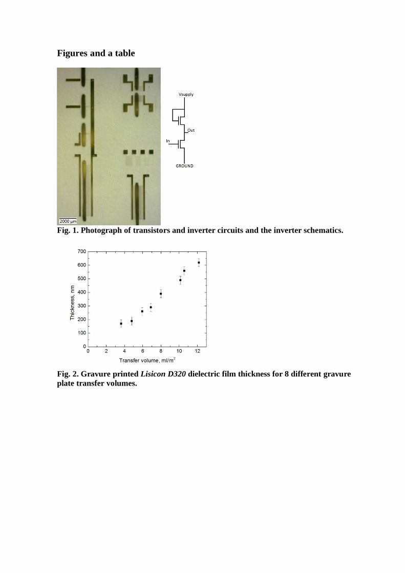
PET substrates with pre-patterned gold electrodes were cleaned and used withoutadhesion related pre-treatment. Printing was done with Schläfli Labratester gravureprinter in normal laboratory environment. Machine dependent printing settings were:speed 6 m/min and pressure dial at 4.2. Gravure printing test plate had 8 different linedensities. Transfer volumes of the gravure plate cells were measured with NanofocusµSurf optical profilometer. Printed sample was dried in oven at 100°C for 20 minutes.Both semiconductor and dielectric were printed with the same plate and dried the sameway. Printed film thicknesses were measured with Dektak 150 profilometer. Several setsof film thickness combinations were printed. The transistor structures were completed bytop gate deposition (40 nm gold) through a shadow mask in the thermal vacuumevaporator. Transistors from the best set were connected together in diode connected loadconfiguration (enhancement mode driver and load transistors) [13], forming invertercircuits (Fig. 1).
3 RESULTS AND DISCUSSION
3.1 Transistors using Lisicon D320 dielectric
The printed semiconductor was 10-80 nm and dielectric 200-560 nm thick. Thicknesswas proportional to the transfer volume of the cells (Fig. 2). Ink transfer ratio fromgravure cells to the substrate was over 50%, which is remarkably high [14]. The printedsemiconductor film quality was poor, as there were thickness variations and some wettingdifferences on the substrate and the gold film. Still the semiconductor formed acontinuous layer on top of the interdigitated source and drain electrodes. The dielectricfilm had better quality. There were only minor thickness variations. Edge quality islimited by the gravure cell size (Fig. 3). Dimensions of the test transistors were: channellength 5-20 µm, channel width 8-80 mm.
Electrical measurements show that even though the semiconductor film seemed to havepoor quality, the transistors work very well. The performance of the printed transistor issimilar or better than the spin coated reference transistor with roughly the same
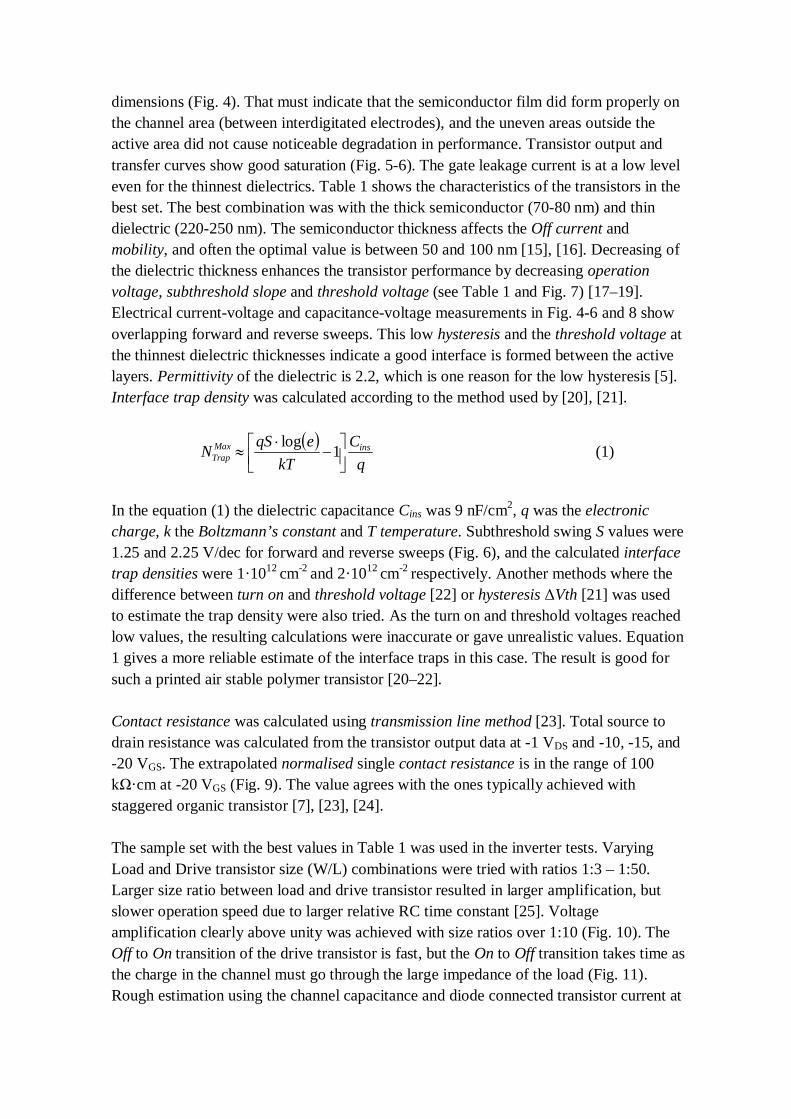
dimensions (Fig. 4). That must indicate that the semiconductor film did form properly onthe channel area (between interdigitated electrodes), and the uneven areas outside theactive area did not cause noticeable degradation in performance. Transistor output andtransfer curves show good saturation (Fig. 5-6). The gate leakage current is at a low leveleven for the thinnest dielectrics. Table 1 shows the characteristics of the transistors in thebest set. The best combination was with the thick semiconductor (70-80 nm) and thindielectric (220-250 nm). The semiconductor thickness affects the Off current andmobility, and often the optimal value is between 50 and 100 nm [15], [16]. Decreasing ofthe dielectric thickness enhances the transistor performance by decreasing operationvoltage, subthreshold slope and threshold voltage (see Table 1 and Fig. 7) [17–19].Electrical current-voltage and capacitance-voltage measurements in Fig. 4-6 and 8 showoverlapping forward and reverse sweeps. This low hysteresis and the threshold voltage atthe thinnest dielectric thicknesses indicate a good interface is formed between the activelayers. Permittivity of the dielectric is 2.2, which is one reason for the low hysteresis [5].Interface trap density was calculated according to the method used by [20], [21].
qC
kTeqSN insMax
Trap 1log (1)
In the equation (1) the dielectric capacitance Cins was 9 nF/cm2, q was the electroniccharge, k the Boltzmann’s constant and T temperature. Subthreshold swing S values were1.25 and 2.25 V/dec for forward and reverse sweeps (Fig. 6), and the calculated interfacetrap densities were 1·1012 cm-2 and 2·1012 cm-2 respectively. Another methods where thedifference between turn on and threshold voltage [22] or hysteresis Vth [21] was usedto estimate the trap density were also tried. As the turn on and threshold voltages reachedlow values, the resulting calculations were inaccurate or gave unrealistic values. Equation1 gives a more reliable estimate of the interface traps in this case. The result is good forsuch a printed air stable polymer transistor [20–22].
Contact resistance was calculated using transmission line method [23]. Total source todrain resistance was calculated from the transistor output data at -1 VDS and -10, -15, and-20 VGS. The extrapolated normalised single contact resistance is in the range of 100
·cm at -20 VGS (Fig. 9). The value agrees with the ones typically achieved withstaggered organic transistor [7], [23], [24].
The sample set with the best values in Table 1 was used in the inverter tests. VaryingLoad and Drive transistor size (W/L) combinations were tried with ratios 1:3 – 1:50.Larger size ratio between load and drive transistor resulted in larger amplification, butslower operation speed due to larger relative RC time constant [25]. Voltageamplification clearly above unity was achieved with size ratios over 1:10 (Fig. 10). TheOff to On transition of the drive transistor is fast, but the On to Off transition takes time asthe charge in the channel must go through the large impedance of the load (Fig. 11).Rough estimation using the channel capacitance and diode connected transistor current at
the working voltage yields the time constant of ~0.2 seconds, which is about the same asshown in the Fig. 11. Working inverter shows the potentiality of the use of printedpolymer transistors in more complex logic circuits even at low voltages.
3.2 Transistors using PMMA dielectric
Transistors were also made with similar process but replacing the D320 dielectric withPMMA. The printed dielectric layers were very thin, dropping the yield of the pinholefree processing to less than 40% for 190-180 nm thick and to 0% for thinner layers.Again the threshold voltage was very low, between -0.5 and 1.5 volts for all thetransistors measured. Subthreshold slope was 1.0-1.8 V/dec and 3.1-3.5 V/dec forforward and reverse sweeps respectively. But the mobility was 0.0005 cm2/(Vs), whenwith Lisicon D320 dielectric it was 0.04 cm2/(Vs). As the other values do not indicateproblems, the reason for the mobility degradation could indeed be the energetic disorderand enhanced charge carrier localization suggested by [5]. The more polar PMMA witha permittivity between 3.3 and 3.9 has larger polarization effect reaching through theinterface to the active semiconductor layer. The active layer of this semiconductor issensitive to the polarization effect, but it obviously does not indicate that PMMA wouldnot work with other semiconductors [26].
4 Conclusions
The results show that with modern materials an air stable and hysteresis free gravureprinted transistors and inverters can operate at low voltages. The studied materialcombination is otherwise excellent, but the semiconductor is inherently limited by itsmobility. More recent polymer semiconductors with mobility between 0.1 and 1 mayprove to be as well printed in thin layers, thus making low cost large area electronicspossible with a performance close to amorphous silicon and small molecules.
References
[1] P. Kopola, M. Tuomikoski, R. Suhonen, A. Maaninen, Thin Solid Films 517(2009) 5757.
[2] J.-M. Verilhac, M. Benwadih, A.-L. Seiler, S. Jacob, C. Bory, J. Bablet, M.Heitzman, J. Tallal, L. Barbut, P. Frère, G. Sicard, R. Gwoziecki, I. Chartier, R.Coppard, C. Serbutoviez, Organic Electronics 11 (2010) 456.
[3] M. Hambsch, K. Reuter, M. Stanel, G. Schmidt, H. Kempa, U. Fügmann, U.Hahn, A.C.C. Hübler, Materials Science and Engineering B 170 (2010) 93.
[4] H. Yan, Z. Chen, Y. Zheng, C. Newman, J.R. Quinn, F. Dötz, M. Kastler, A.Facchetti, Nature 457 (2009) 679.
[5] M.M. Voigt, A. Guite, D.-Y. Chung, R.U. a. Khan, A.J. Campbell, D.D.C.Bradley, F. Meng, J.H.G. Steinke, S. Tierney, I. McCulloch, H. Penxten, L.Lutsen, O. Douheret, J. Manca, U. Brokmann, K. Sönnichsen, D. Hülsenberg, W.Bock, C. Barron, N. Blanckaert, S. Springer, J. Grupp, A. Mosley, AdvancedFunctional Materials 20 (2010) 239.
[6] P. Kopola, T. Aernouts, S. Guillerez, H. Jin, M. Tuomikoski, A. Maaninen, J.Hast, Solar Energy Materials and Solar Cells 94 (2010) 1673.
[7] J. Veres, S.D. Ogier, S.W. Leeming, D.C. Cupertino, S. Mohialdin Khaffaf,Advanced Functional Materials 13 (2003) 199.
[6] A. de la Fuente Vornbrock, D. Sung, H. Kang, R. Kitsomboonloha, V.Subramanian, Organic Electronics 11 (2010) 2037.
[9] H. Kang, R. Kitsomboonloha, J. Jang, V. Subramanian, Advanced Materials 24(2012) 3065.
[10] H. Kempa, M. Hambsch, K. Reuter, M. Stanel, G. C. Schmidt, B. Meier, A.C.Hübler, IEEE Trans. Electron Devices 58 (2011) 2765.
[11] G. C. Schmidt, M. Bellmann, B. Meier, M. Hambsch, K. Reuter, H. Kempa,A.C. Hübler, Organic Electronics 11 (2010) 1683.
[12] C. Kim, Z. Wang, H.-J. Choi, Y.-G. Ha, A. Facchetti, T. J. Marks, Journal of theAmerican Chemical Society 130 (2008) 6867.
[13] H.-Y. Tseng, V. Subramanian, Organic Electronics 12 (2011) 249.
[14] X. Yin, S. Kumar, Chemical Engineering Science 61 (2006) 1146.
[15] S. Hoshino, T. Kamata, K. Yase, Journal of Applied Physics 92 (2002) 6028.
[16] H. Jia, S. Gowrisanker, G.K. Pant, R.M. Wallace, B.E. Gnade, Journal ofVacuum Science Technology A Vacuum Surfaces and Films 24 (2006) 1228.
[17] N. Gupta, Physica Scripta 76 (2007) 628.
[18] G. Paasch, S. Scheinert, Materials SciencePoland 22 (2004) 423.
[19] J. Veres, S. Ogier, G. Lloyd, D. De Leeuw, Chemistry of Materials 16 (2004)4543.
[20] L.T.L. Teng, W.A Anderson, IEEE Electron Device Letters 24 (2003) 399.
[21] M. McDowell, I.G. Hill, J.E. McDermott, S.L. Bernasek, J. Schwartz, AppliedPhysics Letters 88 (2006) 073505.
[22] K.P. Pernstich, S. Haas, D. Oberhoff, C. Goldmann, D.J. Gundlach, B. Batlogg,A. N. Rashid, G. Schitter, Journal of Applied Physics 96 (2004) 6431.
[23] P. V Necliudov, M.S. Shur, D.J. Gundlach, T.N. Jackson, 2001 InternationalSemiconductor Device Research Symposium Symposium Proceedings 47 (2001)259.
[24] D. Boudinet, M. Benwadih, S. Altazin, R. Gwoziecki, J.M. Verilhac, R. Coppard,G. Le Blevennec, I. Chartier, G. Horowitz, Organic Electronics 11 (2010) 291.
[25] G.H. Gelinck, T.C.T. Geuns, D.M. de Leeuw, Applied Physics Letters 77 (2000)1487.
[26] R. Ponce Ortiz, A. Facchetti, T.J. Marks, Chemical Reviews 110 (2010) 205.
Figures and a table
Fig. 1. Photograph of transistors and inverter circuits and the inverter schematics.
Fig. 2. Gravure printed Lisicon D320 dielectric film thickness for 8 different gravureplate transfer volumes.
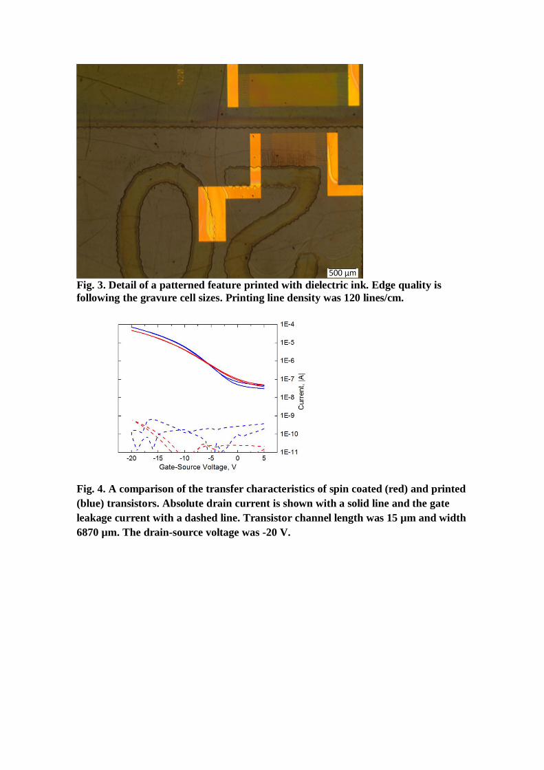
Fig. 3. Detail of a patterned feature printed with dielectric ink. Edge quality isfollowing the gravure cell sizes. Printing line density was 120 lines/cm.
Fig. 4. A comparison of the transfer characteristics of spin coated (red) and printed(blue) transistors. Absolute drain current is shown with a solid line and the gateleakage current with a dashed line. Transistor channel length was 15 µm and width6870 µm. The drain-source voltage was -20 V.
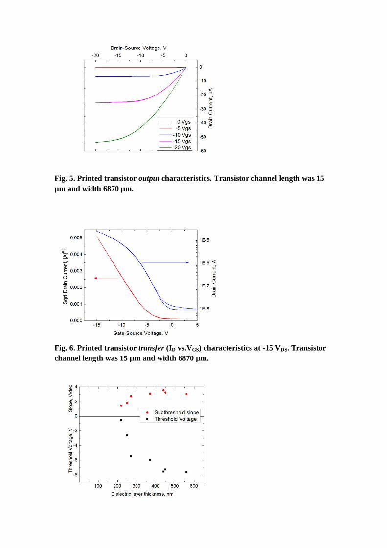
Fig. 5. Printed transistor output characteristics. Transistor channel length was 15µm and width 6870 µm.
Fig. 6. Printed transistor transfer (ID vs.VGS) characteristics at -15 VDS. Transistorchannel length was 15 µm and width 6870 µm.
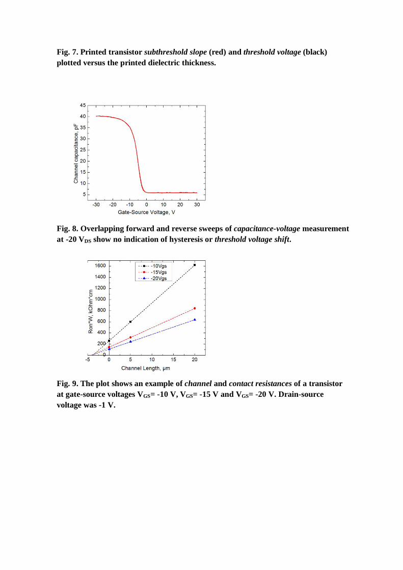
Fig. 7. Printed transistor subthreshold slope (red) and threshold voltage (black)plotted versus the printed dielectric thickness.
Fig. 8. Overlapping forward and reverse sweeps of capacitance-voltage measurementat -20 VDS show no indication of hysteresis or threshold voltage shift.
Fig. 9. The plot shows an example of channel and contact resistances of a transistorat gate-source voltages VGS= -10 V, VGS= -15 V and VGS= -20 V. Drain-sourcevoltage was -1 V.
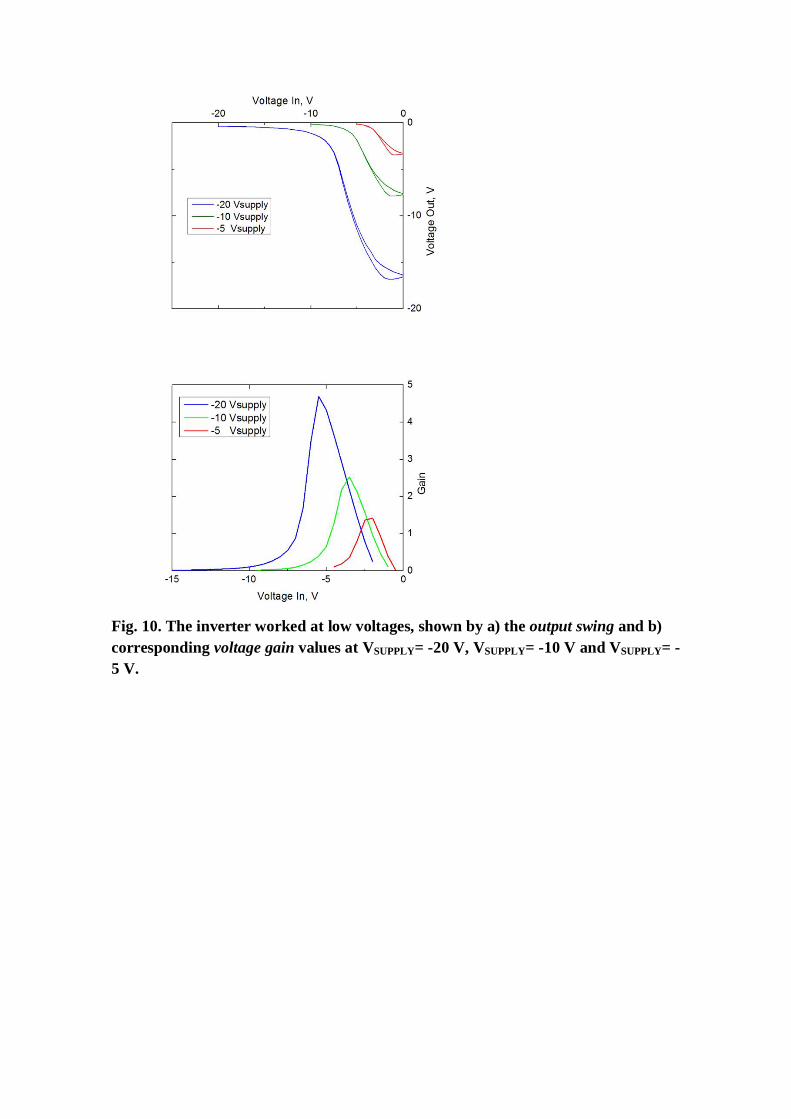
Fig. 10. The inverter worked at low voltages, shown by a) the output swing and b)corresponding voltage gain values at VSUPPLY= -20 V, VSUPPLY= -10 V and VSUPPLY= -5 V.

Fig. 11. Inverter dynamic characteristics are presented by the response to a 0 to -5 Vsquare wave input signal. In a) the inverter had a load:drive size ratio of 1:10 and inb) 1:30. The long On to Off transition (closing) of the drive transistor is shownclearly. In b) the step time scale is different in order to show the full tail of thetransition.
Dielectric thickness, nm 560 440 450 370 270 250 220
Mobility, cm2/(Vs) 0.01 0.02 0.02 0.03 0.02 0.04 0.03
Threshold voltage, V -7.6 -7.5 -7.2 -5.9 -5.5 -2.6 -0.5
On/Off ratio 4 000 1 400 2 200 6 800 4 000 7 500 6 500
Subthreshold slope, V/dec 3 3.6 3.2 3.1 2.7 1.8 1.4
Table 1. The transistor characteristics of a printed sample series with differentdielectric thicknesses.