Embed Size (px)
Citation preview
CIS 371 (Martin): Digital Logic & Hardware Description 1
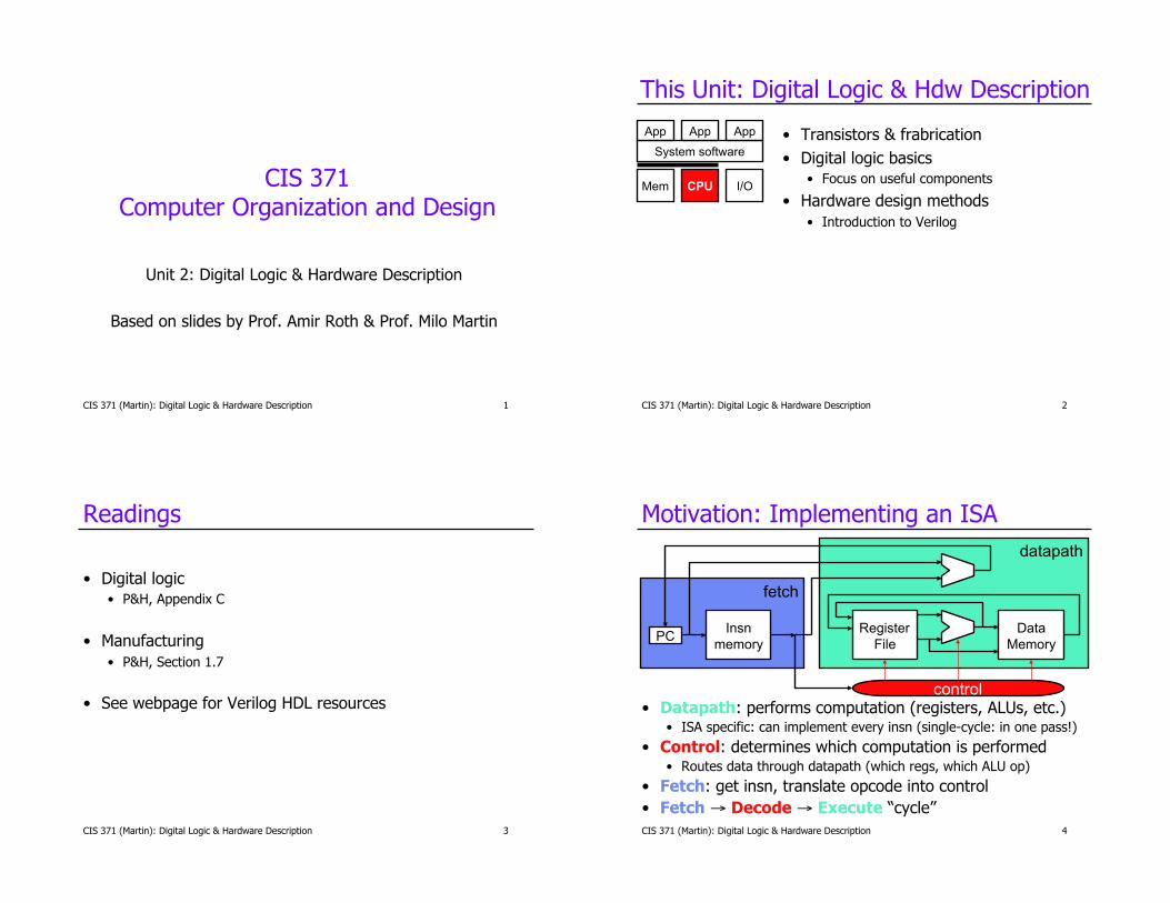
CIS 371 Computer Organization and Design
Unit 2: Digital Logic & Hardware Description
Based on slides by Prof. Amir Roth & Prof. Milo Martin
CIS 371 (Martin): Digital Logic & Hardware Description 2
This Unit: Digital Logic & Hdw Description
• Transistors & frabrication • Digital logic basics
• Focus on useful components
• Hardware design methods • Introduction to Verilog
CPU Mem I/O
System software
App App App
CIS 371 (Martin): Digital Logic & Hardware Description 3
Readings
• Digital logic • P&H, Appendix C
• Manufacturing • P&H, Section 1.7
• See webpage for Verilog HDL resources
CIS 371 (Martin): Digital Logic & Hardware Description 4
Motivation: Implementing an ISA
• Datapath: performs computation (registers, ALUs, etc.) • ISA specific: can implement every insn (single-cycle: in one pass!)
• Control: determines which computation is performed • Routes data through datapath (which regs, which ALU op)
• Fetch: get insn, translate opcode into control • Fetch → Decode → Execute “cycle”
PC Insn
memory Register
File Data
Memory
control
datapath
fetch
CIS 371 (Martin): Digital Logic & Hardware Description 5
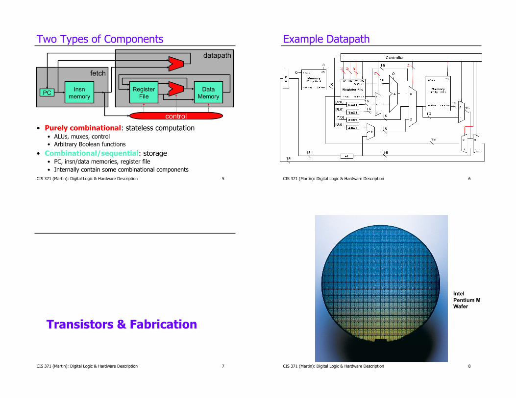
Two Types of Components
• Purely combinational: stateless computation • ALUs, muxes, control • Arbitrary Boolean functions
• Combinational/sequential: storage • PC, insn/data memories, register file • Internally contain some combinational components
PC Insn
memory Register
File Data
Memory
control
datapath
fetch
Example Datapath
CIS 371 (Martin): Digital Logic & Hardware Description 6
Transistors & Fabrication
CIS 371 (Martin): Digital Logic & Hardware Description 7 CIS 371 (Martin): Digital Logic & Hardware Description 8
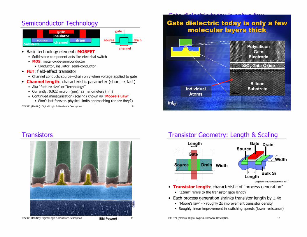
Intel Pentium M Wafer
CIS 371 (Martin): Digital Logic & Hardware Description 9
Semiconductor Technology
• Basic technology element: MOSFET • Solid-state component acts like electrical switch • MOS: metal-oxide-semiconductor
• Conductor, insulator, semi-conductor
• FET: field-effect transistor • Channel conducts source→drain only when voltage applied to gate
• Channel length: characteristic parameter (short → fast) • Aka “feature size” or “technology” • Currently: 0.022 micron (µm), 22 nanometers (nm) • Continued miniaturization (scaling) known as “Moore’s Law”
• Won’t last forever, physical limits approaching (or are they?)
channel source drain insulator
gate
Substrate channel
source drain
gate
Gate dielectric today is only a few molecular layers thick
CIS 371 (Martin): Digital Logic & Hardware Description 10
CIS 371 (Martin): Digital Logic & Hardware Description 11
Transistors ©
IBM
IBM Power6 CIS 371 (Martin): Digital Logic & Hardware Description 12
Transistor Geometry: Length & Scaling
• Transistor length: characteristic of “process generation” • “22nm” refers to the transistor gate length
• Each process generation shrinks transistor length by 1.4x • “Moore’s law” -> roughly 2x improvement transistor density • Roughly linear improvement in switching speeds (lower resistance)
Gate Source
Drain
Bulk Si
Width
Length
Length"
Width"Source Drain
Gate
Diagrams © Krste Asanovic, MIT

CIS 371 (Martin): Digital Logic & Hardware Description 13
Manufacturing Steps
Source: P&H
CIS 371 (Martin): Digital Logic & Hardware Description 14
Manufacturing Steps • Multi-step photo-/electro-chemical process
• More steps, higher unit cost
+ Fixed cost mass production ($1 million+ for “mask set”)
CIS 371 (Martin): Digital Logic & Hardware Description 15
Integrated Circuit (IC) Costs
• Chips built in multi-step chemical processes on wafers • Cost / wafer is constant, f(wafer size, number of steps)
• Chip (die) cost is related to area • Larger chips means fewer of them
• Cost is more than linear in area • Why? random defects • Larger chips means fewer working ones • Chip cost ~ chip areaα"
• α = 2 to 3"
• Wafer yield: % wafer that is chips • Die yield: % chips that work • Yield is increasingly non-binary - fast vs slow chips
CIS 371 (Martin): Digital Logic & Hardware Description 16
Manufacturing Defects
• Defects can arise • Under-/over-doping • Over-/under-dissolved insulator • Mask mis-alignment • Particle contaminants
• Try to minimize defects • Process margins • Design rules
• Minimal transistor size, separation
• Or, tolerate defects • Redundant or “spare” memory cells • Can substantially improve yield
Defective:
Defective:
Slow:
Correct:
CIS 371 (Martin): Digital Logic & Hardware Description 17
Wires Pitch
Width
Length Height
• Transistors 1-dimensional for design purposes: width • Wires 4-dimensional: length, width, height, “pitch”
• Longer wires have more resistance (slower) • “Thinner” wires have more resistance (slower) • Closer wire spacing (“pitch”) increases capacitance (slower)
From slides © Krste Asanovic, MIT
IBM CMOS7, 6 layers of copper wiring
CIS 371 (Martin): Digital Logic & Hardware Description 18
Transistors and Wires
©IB
M
From slides © Krste Asanović, MIT
CIS 371 (Martin): Digital Logic & Hardware Description 19
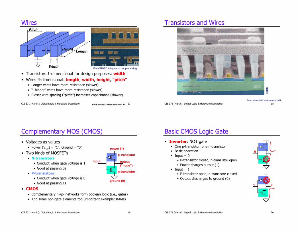
Complementary MOS (CMOS)
• Voltages as values • Power (VDD) = “1”, Ground = “0”
• Two kinds of MOSFETs • N-transistors
• Conduct when gate voltage is 1 • Good at passing 0s
• P-transistors • Conduct when gate voltage is 0 • Good at passing 1s
• CMOS • Complementary n-/p- networks form boolean logic (i.e., gates) • And some non-gate elements too (important example: RAMs)
power (1)
ground (0)
input output (“node”)
n-transistor
p-transistor
CIS 371 (Martin): Digital Logic & Hardware Description 20
Basic CMOS Logic Gate • Inverter: NOT gate
• One p-transistor, one n-transistor • Basic operation • Input = 0
• P-transistor closed, n-transistor open • Power charges output (1)
• Input = 1 • P-transistor open, n-transistor closed • Output discharges to ground (0)
0 1
1 0

CIS 371 (Martin): Digital Logic & Hardware Description
21
Another CMOS Gate Example
• What is this? Look at truth table • 0, 0 → 1 • 0, 1 → 1 • 1, 0 → 1 • 1, 1 → 0 • Result: NAND (NOT AND) • NAND is “universal”
• What function is this?
B A
A
B
output
B
A
A B
output
CIS 371 (Martin): Digital Logic & Hardware Description 22
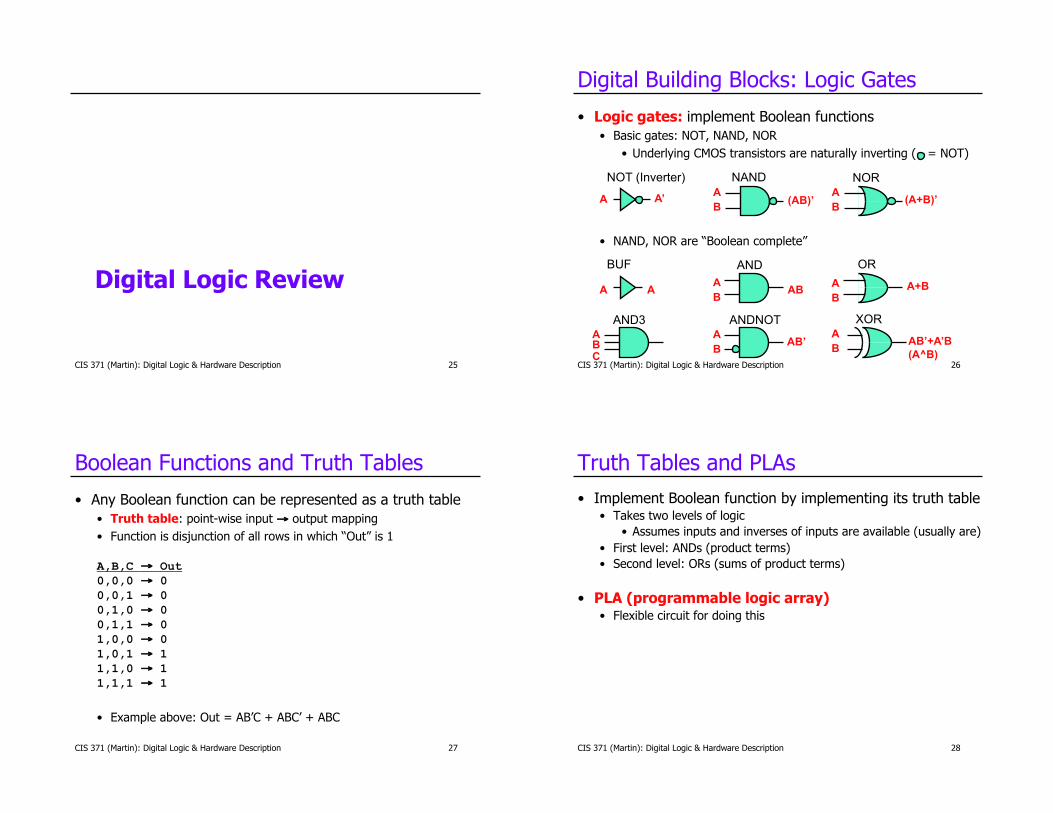
Digital Building Blocks: Logic Gates
• Logic gates: implement Boolean functions • Basic gates: NOT, NAND, NOR
• Underlying CMOS transistors are naturally inverting ( = NOT)
• NAND, NOR are “Boolean complete”
NAND NOR
XOR
NOT (Inverter)
A A’ A B (AB)’ (A+B)’ A
B
BUF OR AND
ANDNOT AND3
A A A B
A B
A B
A B
A B C
AB
AB’ AB’+A’B (A^B)
A+B
CIS 371 (Martin): Digital Logic & Hardware Description 23
Alternative to Fabrication: FPGA • We’ll use FPGAs (Field Programmable Gate Array)
• Also called Programmable Logic Devices (PLDs)
• An FPGA is a special type of programmable chip • Conceptually, contains a grid of gates • The wiring connecting them can be reconfigured electrically
• Using more transistors as switches • Once configured, the FPGA can emulate any digital logic design • Tool converts gate-level design to configuration
• Uses • Hardware prototyping (what “we” are doing) • Low-volume special-purpose hardware • New: computational offload
CIS 371 (Martin): Digital Logic & Hardware Description 24
In Our Lab: Digilent XUP-V2P Boards
• Program FPGA to run LC4 • “The project”
• Hook up keyboard • And VGA • Game on!
• Boards have many features • Use some for debugging
• LEDs, switches
• Other features • Ethernet, flash reader • 256MB SDRAM, audio in/out • Can boot Linux!
Digital Logic Review
CIS 371 (Martin): Digital Logic & Hardware Description 25 CIS 371 (Martin): Digital Logic & Hardware Description 26
Digital Building Blocks: Logic Gates
• Logic gates: implement Boolean functions • Basic gates: NOT, NAND, NOR
• Underlying CMOS transistors are naturally inverting ( = NOT)
• NAND, NOR are “Boolean complete”
NAND NOR
XOR
NOT (Inverter)
A A’ A B (AB)’ (A+B)’ A
B
BUF OR AND
ANDNOT AND3
A A A B
A B
A B
A B
A B C
AB
AB’ AB’+A’B (A^B)
A+B
CIS 371 (Martin): Digital Logic & Hardware Description 27
Boolean Functions and Truth Tables
• Any Boolean function can be represented as a truth table • Truth table: point-wise input → output mapping • Function is disjunction of all rows in which “Out” is 1
A,B,C → Out 0,0,0 → 0 0,0,1 → 0 0,1,0 → 0 0,1,1 → 0 1,0,0 → 0 1,0,1 → 1 1,1,0 → 1 1,1,1 → 1
• Example above: Out = AB’C + ABC’ + ABC
CIS 371 (Martin): Digital Logic & Hardware Description 28
Truth Tables and PLAs • Implement Boolean function by implementing its truth table
• Takes two levels of logic • Assumes inputs and inverses of inputs are available (usually are)
• First level: ANDs (product terms) • Second level: ORs (sums of product terms)
• PLA (programmable logic array) • Flexible circuit for doing this
CIS 371 (Martin): Digital Logic & Hardware Description 29
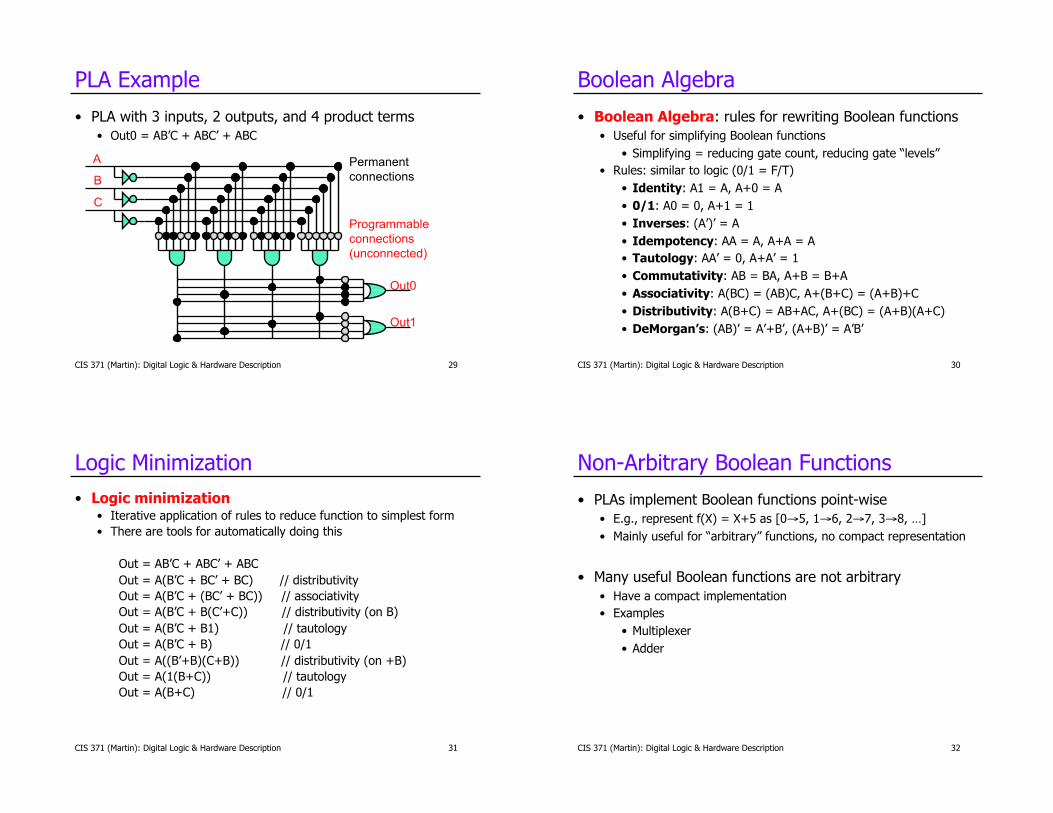
PLA Example
• PLA with 3 inputs, 2 outputs, and 4 product terms • Out0 = AB’C + ABC’ + ABC
A
B
C
Out0
Out1
Permanent connections
Programmable connections (unconnected)
CIS 371 (Martin): Digital Logic & Hardware Description 30
Boolean Algebra
• Boolean Algebra: rules for rewriting Boolean functions • Useful for simplifying Boolean functions
• Simplifying = reducing gate count, reducing gate “levels” • Rules: similar to logic (0/1 = F/T)
• Identity: A1 = A, A+0 = A • 0/1: A0 = 0, A+1 = 1 • Inverses: (A’)’ = A • Idempotency: AA = A, A+A = A • Tautology: AA’ = 0, A+A’ = 1 • Commutativity: AB = BA, A+B = B+A • Associativity: A(BC) = (AB)C, A+(B+C) = (A+B)+C • Distributivity: A(B+C) = AB+AC, A+(BC) = (A+B)(A+C) • DeMorgan’s: (AB)’ = A’+B’, (A+B)’ = A’B’
CIS 371 (Martin): Digital Logic & Hardware Description 31
Logic Minimization • Logic minimization
• Iterative application of rules to reduce function to simplest form • There are tools for automatically doing this
Out = AB’C + ABC’ + ABC Out = A(B’C + BC’ + BC) // distributivity Out = A(B’C + (BC’ + BC)) // associativity Out = A(B’C + B(C’+C)) // distributivity (on B) Out = A(B’C + B1) // tautology Out = A(B’C + B) // 0/1 Out = A((B’+B)(C+B)) // distributivity (on +B) Out = A(1(B+C)) // tautology Out = A(B+C) // 0/1
CIS 371 (Martin): Digital Logic & Hardware Description 32
Non-Arbitrary Boolean Functions
• PLAs implement Boolean functions point-wise • E.g., represent f(X) = X+5 as [0→5, 1→6, 2→7, 3→8, …] • Mainly useful for “arbitrary” functions, no compact representation
• Many useful Boolean functions are not arbitrary • Have a compact implementation • Examples
• Multiplexer • Adder
CIS 371 (Martin): Digital Logic & Hardware Description 33
Multiplexer (Mux)
• Multiplexer (mux): selects output from N inputs • Example: 1-bit 4-to-1 mux • Not shown: N-bit 4-to-1 mux = N 1-bit 4-to-1 muxes + 1 decoder
A
O B
C
D
S (binary)
S (binary)
A B C D
O
S (1-hot)
CIS 371 (Martin): Digital Logic & Hardware Description 34
Adder
• Adder: adds/subtracts two 2C binary integers • Half adder: adds two 1-bit “integers”, no carry-in • Full adder: adds three 1-bit “integers”, includes carry-in • Ripple-carry adder: N chained full adders add 2 N-bit integers • To subtract: negate B input, set bit 0 carry-in to 1
CIS 371 (Martin): Digital Logic & Hardware Description 35
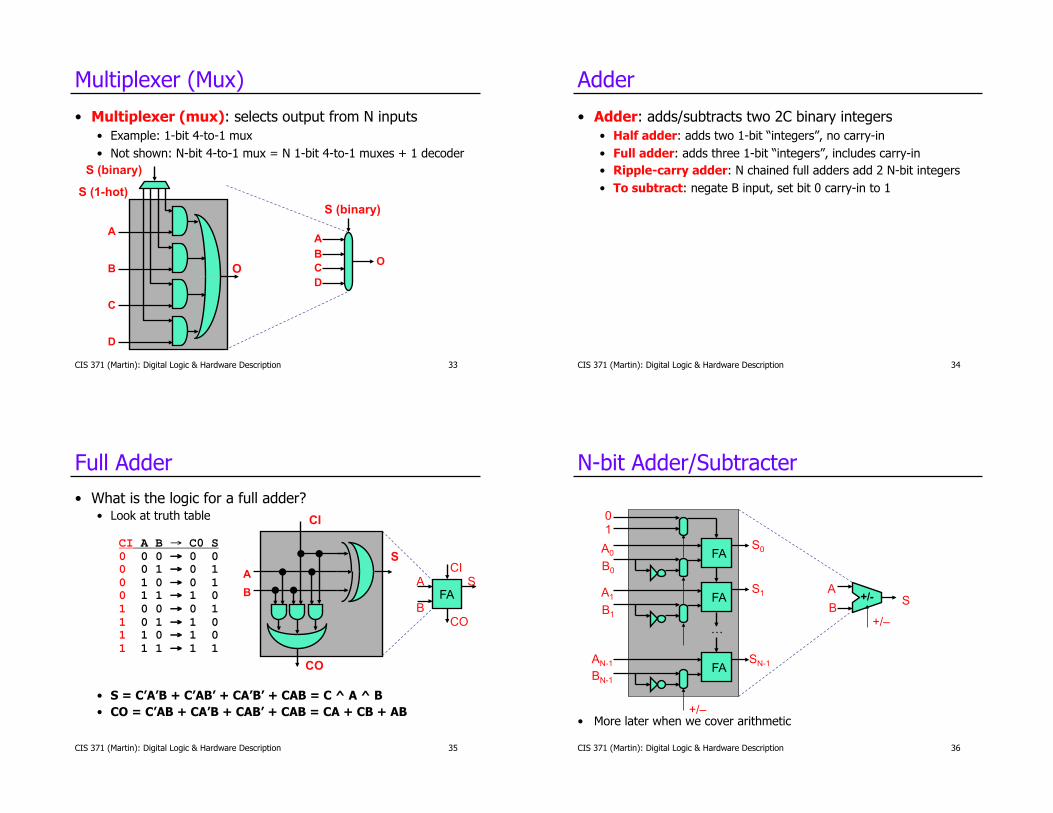
Full Adder • What is the logic for a full adder?
• Look at truth table
CI A B → C0 S 0 0 0 → 0 0 0 0 1 → 0 1 0 1 0 → 0 1 0 1 1 → 1 0 1 0 0 → 0 1 1 0 1 → 1 0 1 1 0 → 1 0 1 1 1 → 1 1
• S = C’A’B + C’AB’ + CA’B’ + CAB = C ^ A ^ B • CO = C’AB + CA’B + CAB’ + CAB = CA + CB + AB
FA B
S
CO
A CI A
B
S
CI
CO
CIS 371 (Martin): Digital Logic & Hardware Description 36
N-bit Adder/Subtracter
S +/- FA B1
S1 A1
FA B0
S0 A0
FA BN-1
SN-1 AN-1
1
…
0
+/–
+/– B
A
• More later when we cover arithmetic
Hardware Design Methods
CIS 371 (Martin): Digital Logic & Hardware Description 37 CIS 371 (Martin): Digital Logic & Hardware Description 38
Hardware Design Methodologies
• Fabricating a chip requires a detailed layout • All transistors & wires
• How does a hardware designer describe such design? • (Bad) Option #1: draw all the masks “by hand”
• All 1 billion transistors? Umm… • Option #2: use computer-aided design (CAD) tools to help
• Layout done by engineers with CAD tools or automatically
• Design levels – uses abstraction • Transistor-level design – designer specifies transistors (not layout) • Gate-level design – designer specifics gates, wires (not transistors) • Higher-level design – designer uses higher-level building blocks
• Adders, memories, etc. • Or logic in terms of and/or/not, and tools translates into gate
Describing Hardware
• Two general options
• Schematics • Pictures of gates & wires
• Hardware description languages • Use textural descriptions to specify hardware
• Translation process called “synthesis” • Textural description -> gates -> full layout
• Tries to minimizes the delay and/or number of gates • Much like process of compilation of software
CIS 371 (Martin): Digital Logic & Hardware Description 39 CIS 371 (Martin): Digital Logic & Hardware Description 40
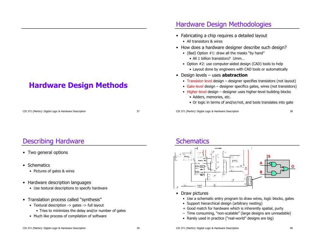
Schematics
• Draw pictures • Use a schematic entry program to draw wires, logic blocks, gates • Support hierarchical design (arbitrary nesting) + Good match for hardware which is inherently spatial, purty – Time consuming, “non-scalable” (large designs are unreadable) • Rarely used in practice (“real-world” designs are big)
S
O B
A

CIS 371 (Martin): Digital Logic & Hardware Description 41
Hardware Description Languages (HDLs) • Write “code” to describe hardware
• HDL vs. SDL • Specify wires, gates, modules (also hierarchical) + Easier to create, edit, modify, scales well – Disconnect: must still “think” visually (gets easier with practice)
module mux2to1(S, A, B, Out);!!input S, A, B;!!output Out;!!wire S_, AnS_, BnS;!
!not (S_, S);!!and (AnS_, A, S_);!!and (BnS, B, S);!!or (Out, AnS_, BnS);!
endmodule!
S
Out B
A
CIS 371 (Martin): Digital Logic & Hardware Description 42
(Hierarchical) HDL Example
• Build up more complex modules using simpler modules • Example: 4-bit wide mux from four 1-bit muxes
module mux2to1_4(S, A, B, Out);! input [3:0] A;! input [3:0] B;! input S;! output [3:0] Out;!
mux2to1 mux0 (S, A[0], B[0], Out[0]);! mux2to1 mux1 (S, A[1], B[1], Out[1]);!! mux2to1 mux2 (S, A[2], B[2], Out[2]);! mux2to1 mux3 (S, A[3], B[3], Out[3]);!endmodule!
S 4
4 4 A
B Out
CIS 371 (Martin): Digital Logic & Hardware Description 43
Verilog HDL
• Verilog: HDL we will be using • Syntactically similar to C (by design) ± Ease of syntax hides fact that this isn’t C (or any SDL) • We will use a few lectures to learn Verilog
module mux2to1_4(S, A, B, Out);! input [3:0] A;! input [3:0] B;! input S;! output [3:0] Out;!
mux2to1 mux0 (S, A[0], B[0], Out[0]);! mux2to1 mux1 (S, A[1], B[1], Out[1]);!! mux2to1 mux2 (S, A[2], B[2], Out[2]);! mux2to1 mux3 (S, A[3], B[3], Out[3]);!endmodule!
These aren’t variables
These aren’t function calls
CIS 371 (Martin): Digital Logic & Hardware Description 44
HDLs are not SDLs (PLs)
• Similar in some (intentional) ways … • Syntax
• Named entities, constants, scoping, etc. • Tool chain: synthesis tool analogous to compiler
• Multiple levels of representation • “Optimization” • Multiple targets (portability)
• “Software” engineering • Modular structure and parameterization • Libraries and code repositories
• … but different in many others • One of the most difficult conceptual leaps of this course
CIS 371 (Martin): Digital Logic & Hardware Description 45
Hardware is not Software
• Just two different beasts (or two parts of the same beast) • Things that make sense in hardware, don’t in software, vice versa • One of the main themes of 371
• Software is sequential • Hardware is inherently parallel, at multiple levels • Have to work to get hardware to not do things in parallel
• Software atoms are purely functional (“digital”) • Hardware atoms have quantitative (“analog”) properties too • Including correctness properties!
• Software mostly about quality (“functionality”) • Hardware mostly about quantity: performance, area, power, etc.
• One reason that HDLs are not SDLs CIS 371 (Martin): Digital Logic & Hardware Description 46
HDL: Behavioral Constructs
• HDLs have low-level structural constructs • Specify hardware structures directly • Transistors, gates (and, not) and wires, hierarchy via modules
• Also have mid-level behavioral constructs • Specify operations, not hardware to perform them • Low-to-medium-level: &, ~, +, *
• Also higher-level behavioral constructs • High-level: if-then-else, for loops • Some of these are synthesizable (some are not)
• Tools try to guess what you want, often highly inefficient – Higher-level → more difficult to know what it will synthesize to!
• HDLs are both high- and low-level languages in one! • And the boundary is not clear!
CIS 371 (Martin): Digital Logic & Hardware Description 47
HDL: Simulation
• Another use of HDL: simulating & testing a hardware design • Cheaper & faster turnaround (no need to fabricate) • More visibility into design (“debugger” interface)
• HDLs have features just for simulation • Higher level data types: integers, FP-numbers, timestamps • Higher level control structures: for-loops, conditionals • Routines for I/O: error messages, file operations • Obviously, these cannot be synthesized into circuits
• Also another reason for HDL/SDL confusion • HDLs have “SDL” features for simulation
Verilog HDL
CIS 371 (Martin): Digital Logic & Hardware Description 48

CIS 371 (Martin): Digital Logic & Hardware Description 49
HDL History • 1970s:
• First HDLs
• Late 1970s: VHDL • VHDL = VHSIC HDL = Very High Speed Integrated Circuit HDL • VHDL inspired by programming languages of the day (Ada)
• 1980s: • Verilog first introduced • Verilog inspired by the C programming language • VHDL standardized
• 1990s: • Verilog standardized (Verilog-1995 standard)
• 2000s: • Continued evolution (Verilog-2001 standard)
• Both VHDL and Verilog evolving, still in use today
CIS 371 (Martin): Digital Logic & Hardware Description 50
Verilog HDL
• Verilog is a (surprisingly) big language • Structural constructs at both gate and transistor level • Facilities for specifying memories • Precise timing specification and simulation • Lots of “behavioral” constructs • C-style procedural variables, including arrays • A pre-processor • VPI: Verilog programming interface • …
CIS 371 (Martin): Digital Logic & Hardware Description 51
371 Verilog HDL
• We’re going to learn a focused subset of Verilog • Focus on synthesizable constructs • Focus on avoiding subtle synthesis errors • Use as an educational tool
• For synthesis • Structural constructs at gate-level only • A few behavioral constructs
• Some testing and debugging features
Rule 1: if you haven’t seen it in lecture, you can’t use it!
Rule 1a: when in doubt, ask!
CIS 371 (Martin): Digital Logic & Hardware Description 52
Basic Verilog Syntax
• Have already seen basic syntax, looks like C • C/C++/Java style comments • Names are case sensitive, and can use _ (underscore) • Avoid: clock, clk, power, pwr, ground, gnd, vdd, vcc, init, reset, rst
• Some of these are “special” and will silently cause errors
/* this is a module */!module mux2to1(S, A, B, Out);!
!input S, A, B;!!output Out;!!wire S_, AnS_, BnS;!!// these are gates!!not (S_, S);!!and (AnS_, A, S_);!!and (BnS, B, S);!!or (Out, AnS_, BnS);!
endmodule!
CIS 371 (Martin): Digital Logic & Hardware Description 53
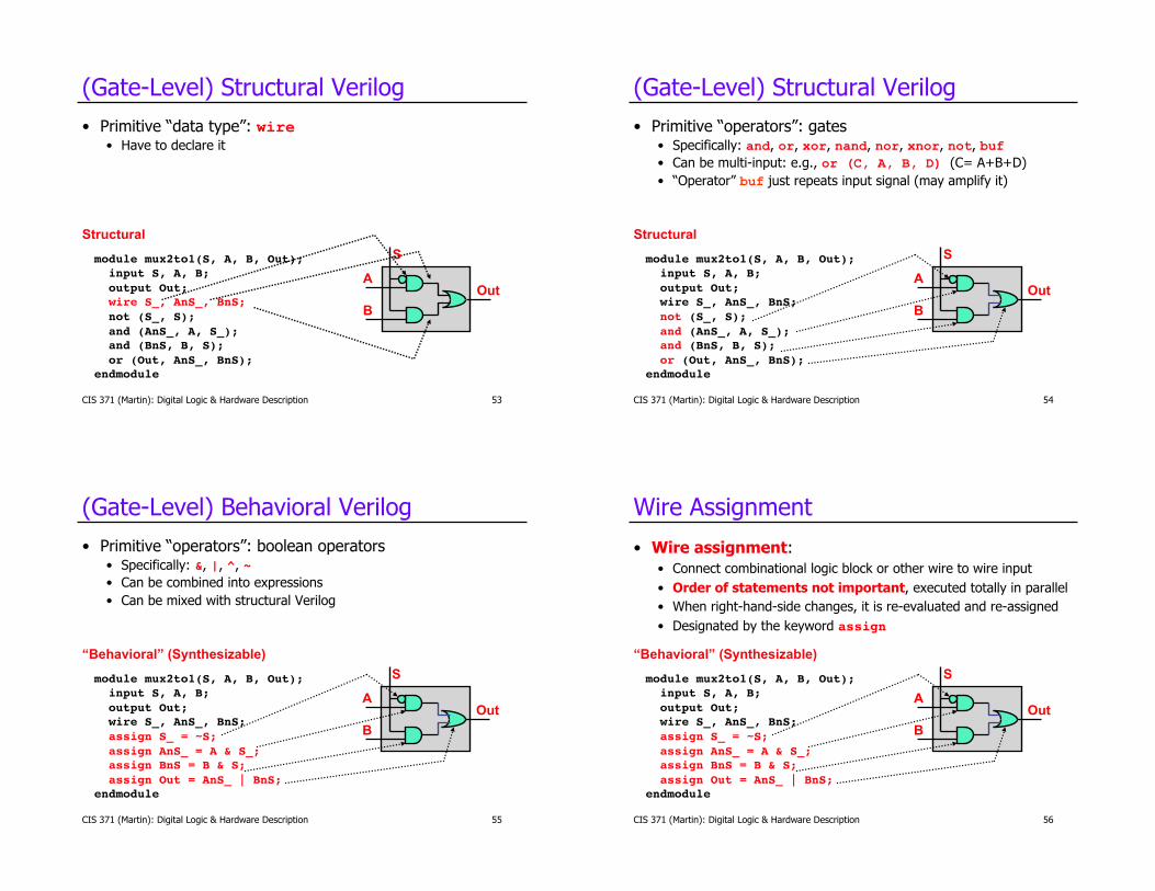
(Gate-Level) Structural Verilog
module mux2to1(S, A, B, Out);! input S, A, B;! output Out;! wire S_, AnS_, BnS;! not (S_, S);! and (AnS_, A, S_);! and (BnS, B, S);! or (Out, AnS_, BnS);!endmodule!
S
Out B
A
• Primitive “data type”: wire • Have to declare it
Structural
CIS 371 (Martin): Digital Logic & Hardware Description 54
(Gate-Level) Structural Verilog
module mux2to1(S, A, B, Out);! input S, A, B;! output Out;! wire S_, AnS_, BnS;! not (S_, S);! and (AnS_, A, S_);! and (BnS, B, S);! or (Out, AnS_, BnS);!endmodule!
• Primitive “operators”: gates • Specifically: and, or, xor, nand, nor, xnor, not, buf • Can be multi-input: e.g., or (C, A, B, D) (C= A+B+D) • “Operator” buf just repeats input signal (may amplify it)
S
Out B
A
Structural
CIS 371 (Martin): Digital Logic & Hardware Description 55
(Gate-Level) Behavioral Verilog • Primitive “operators”: boolean operators
• Specifically: &, |, ^, ~ • Can be combined into expressions • Can be mixed with structural Verilog
module mux2to1(S, A, B, Out);! input S, A, B;! output Out;! wire S_, AnS_, BnS;! assign S_ = ~S;! assign AnS_ = A & S_;! assign BnS = B & S;! assign Out = AnS_ | BnS;!endmodule!
S
Out B
A
“Behavioral” (Synthesizable)
CIS 371 (Martin): Digital Logic & Hardware Description 56
Wire Assignment
• Wire assignment: • Connect combinational logic block or other wire to wire input • Order of statements not important, executed totally in parallel • When right-hand-side changes, it is re-evaluated and re-assigned • Designated by the keyword assign!
module mux2to1(S, A, B, Out);! input S, A, B;! output Out;! wire S_, AnS_, BnS;! assign S_ = ~S;! assign AnS_ = A & S_;! assign BnS = B & S;! assign Out = AnS_ | BnS;!endmodule!
S
Out B
A
“Behavioral” (Synthesizable)
CIS 371 (Martin): Digital Logic & Hardware Description 57
Wire Assignment • Assignment can be combined with declaration
wire c = a | b;!
module mux2to1(S, A, B, Out);! input S, A, B;! output Out;!
wire S_ = ~S;! wire AnS_ = A & S_;! wire BnS = B & S;! assign Out = AnS_ | BnS;!endmodule!
S
Out B
A
“Behavioral” (Synthesizable)
CIS 371 (Martin): Digital Logic & Hardware Description 58
(Gate-Level) Behavioral Verilog
S
Out B
A
• Primitive “operators”: boolean operators • Specifically: &, |, ^, ~ • Can be combined into expressions • Can be mixed with structural Verilog
“Behavioral” (Synthesizable)
module mux2to1(S, A, B, Out);! input S, A, B;! output Out;!
assign Out = (~S & A) | (S & B);!endmodule!
CIS 371 (Martin): Digital Logic & Hardware Description 59
Easiest Way to do a Mux?
• Verilog supports ?: conditional assignment operator • Much more useful (and common) in Verilog than in C/Java
S
Out B
A module mux2to1(S, A, B, Out);! input S, A, B;! output Out;!
assign Out = S ? B : A; !endmodule!
“Behavioral” (Synthesizable)
CIS 371 (Martin): Digital Logic & Hardware Description 60
Wires Are Not C-like Variables!
• Order of assignment doesn’t matter • This works fine module mux2to1(S, A, B, Out);! input S, A, B;! output Out;! wire S_, AnS_, BnS;! assign Out = AnS_ | BnS;! assign BnS = B & S;! assign AnS_ = A & S_;! assign S_ = ~S;!endmodule!
• Can’t “reuse” a wire assign temp = a & b;!assign temp = a | b;!• Actually, you can; but doesn’t do what you think it does
CIS 371 (Martin): Digital Logic & Hardware Description 61
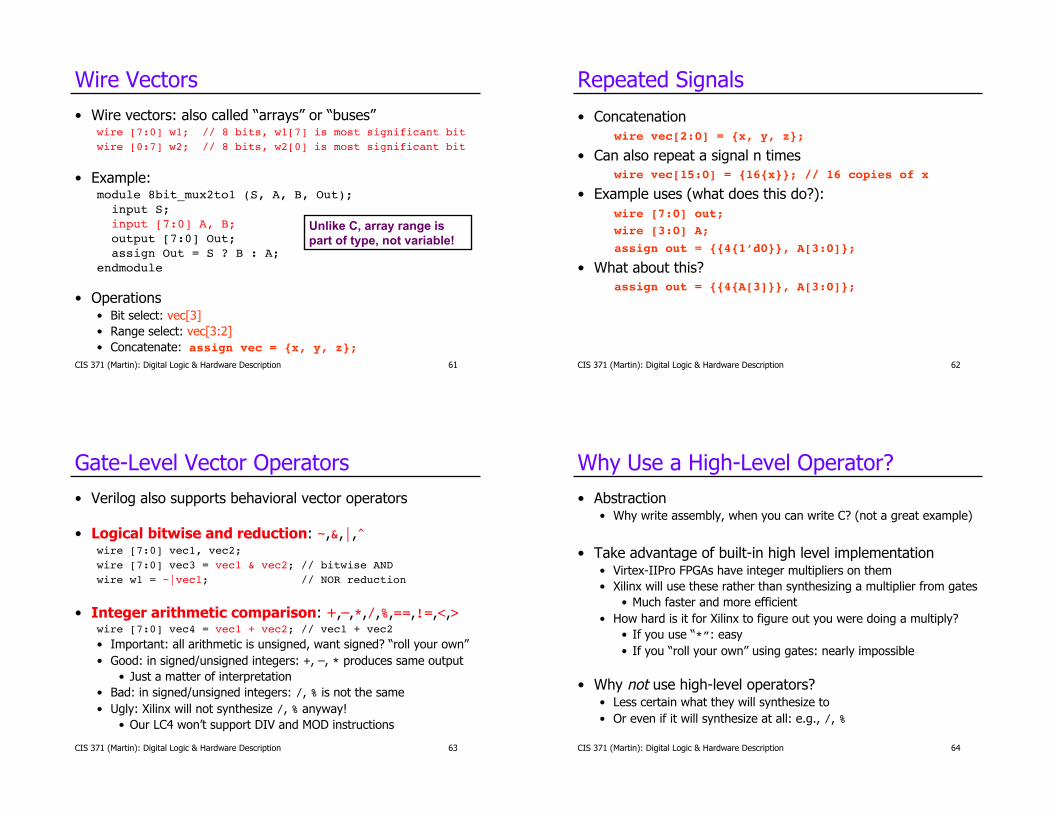
Wire Vectors • Wire vectors: also called “arrays” or “buses”!
wire [7:0] w1; // 8 bits, w1[7] is most significant bit!wire [0:7] w2; // 8 bits, w2[0] is most significant bit!
• Example: module 8bit_mux2to1 (S, A, B, Out);! input S;! input [7:0] A, B;! output [7:0] Out;! assign Out = S ? B : A; !endmodule!
• Operations • Bit select: vec[3] • Range select: vec[3:2] • Concatenate: assign vec = {x, y, z};!
Unlike C, array range is part of type, not variable!
CIS 371 (Martin): Digital Logic & Hardware Description 62
Repeated Signals
• Concatenation wire vec[2:0] = {x, y, z};!• Can also repeat a signal n times wire vec[15:0] = {16{x}}; // 16 copies of x!• Example uses (what does this do?): wire [7:0] out;! wire [3:0] A; assign out = {{4{1’d0}}, A[3:0]};!• What about this? assign out = {{4{A[3]}}, A[3:0]};!
CIS 371 (Martin): Digital Logic & Hardware Description 63
Gate-Level Vector Operators • Verilog also supports behavioral vector operators
• Logical bitwise and reduction: ~,&,|,^ wire [7:0] vec1, vec2;!wire [7:0] vec3 = vec1 & vec2; // bitwise AND!wire w1 = ~|vec1; // NOR reduction !
• Integer arithmetic comparison: +,–,*,/,%,==,!=,<,> wire [7:0] vec4 = vec1 + vec2; // vec1 + vec2!• Important: all arithmetic is unsigned, want signed? “roll your own” • Good: in signed/unsigned integers: +, –, * produces same output
• Just a matter of interpretation • Bad: in signed/unsigned integers: /, % is not the same • Ugly: Xilinx will not synthesize /, % anyway!
• Our LC4 won’t support DIV and MOD instructions
CIS 371 (Martin): Digital Logic & Hardware Description 64
Why Use a High-Level Operator? • Abstraction
• Why write assembly, when you can write C? (not a great example)
• Take advantage of built-in high level implementation • Virtex-IIPro FPGAs have integer multipliers on them • Xilinx will use these rather than synthesizing a multiplier from gates
• Much faster and more efficient • How hard is it for Xilinx to figure out you were doing a multiply?
• If you use “*”: easy • If you “roll your own” using gates: nearly impossible
• Why not use high-level operators? • Less certain what they will synthesize to • Or even if it will synthesize at all: e.g., /, %
CIS 371 (Martin): Digital Logic & Hardware Description 65
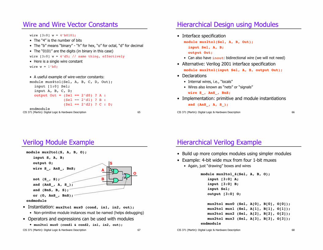
Wire and Wire Vector Constants wire [3:0] w = 4’b0101;!• The “4” is the number of bits • The “b” means “binary” - “h” for hex, “o” for octal, “d” for decimal • The “0101” are the digits (in binary in this case) wire [3:0] w = 4’d5; // same thing, effectively!• Here is a single wire constant wire w = 1’b0; !
• A useful example of wire-vector constants: module mux4to1(Sel, A, B, C, D, Out);! input [1:0] Sel;! input A, B, C, D;! output Out = (Sel == 2’d0) ? A : ! (Sel == 2’d1) ? B :! (Sel == 2’d2) ? C : D; !endmodule!
CIS 371 (Martin): Digital Logic & Hardware Description 66
Hierarchical Design using Modules
• Interface specification module mux2to1(Sel, A, B, Out); !!input Sel, A, B; !!output Out;
• Can also have inout: bidirectional wire (we will not need)
• Alternative: Verilog 2001 interface specification module mux2to1(input Sel, A, B, output Out); !
• Declarations!• Internal wires, i.e., “locals” • Wires also known as “nets” or “signals” !wire S_, AnS_, BnS;!
• Implementation: primitive and module instantiations!!and (AnS_, A, S_);!
CIS 371 (Martin): Digital Logic & Hardware Description 67
module mux2to1(S, A, B, O);!!input S, A, B;!!output O;!!wire S_, AnS_, BnS;!
!not (S_, S);!!and (AnS_, A, S_);!!and (BnS, B, S);!!or (O, AnS_, BnS);!
endmodule!
S
O B
A
Verilog Module Example
• Instantiation: mux2to1 mux0 (cond, in1, in2, out); • Non-primitive module instances must be named (helps debugging)
• Operators and expressions can be used with modules • mux2to1 mux0 (cond1 & cond2, in1, in2, out);!
CIS 371 (Martin): Digital Logic & Hardware Description 68
Hierarchical Verilog Example
• Build up more complex modules using simpler modules • Example: 4-bit wide mux from four 1-bit muxes
• Again, just “drawing” boxes and wires
module mux2to1_4(Sel, A, B, O);!!input [3:0] A;!
input [3:0] B;!!input Sel;!!output [3:0] O;!
!mux2to1 mux0 (Sel, A[0], B[0], O[0]);!!mux2to1 mux1 (Sel, A[1], B[1], O[1]); !!!mux2to1 mux2 (Sel, A[2], B[2], O[2]);!!mux2to1 mux3 (Sel, A[3], B[3], O[3]);!
endmodule!

CIS 371 (Martin): Digital Logic & Hardware Description 69
Connections by Name
• Can (should?) specify module connections by name • Helps keep the bugs away • Example mux2to1 mux0 (.S(Sel), .A(A[0]), .B(B[0]), .O(O[0]));!• Also, then order doesn’t matter!mux2to1 mux1 (.A(A[1]), .B(B[1]), .O(O[1]), .S(Sel));!
CIS 371 (Martin): Digital Logic & Hardware Description 70
Per-Instance Module Parameters • Module parameters: useful for defines varying bus widths
• But for widths, not “types” (in HDL “width” == “type”)!
module Nbit_mux2to1 (Sel, A, B, Out);!! parameter N = 1;!! input [N-1:0] A, B; !
input Sel; ! output [N-1:0] Out;! assign Out = Sel ? B : A;!endmodule!
• Two ways to instantiate: implicit!!!Nbit_mux2to1 #(4) mux1 (S, in1, in2, out); !
• And explicit !!Nbit_mux2to1 mux1 (S, in1, in2, out);!!!defparam mux1.N = 4;
• Multiple parameters per module allowed
CIS 371 (Martin): Digital Logic & Hardware Description 71
Verilog Pre-Processor
• Like the C pre-processor • But uses ` (back-tick) instead of # • Constants: `define!
• No parameterized macros • Use ` before expanding constant macro `define letter_A 8’h41!wire w[7:0] = `letter_A;!
• Conditional compilation: `ifdef, `endif!• File inclusion: `include!
• Parameter vs `define • Parameter only for “per instance” constants • `define for “global” constants
Sequential Logic
CIS 371 (Martin): Digital Logic & Hardware Description 72
CIS 371 (Martin): Digital Logic & Hardware Description 73
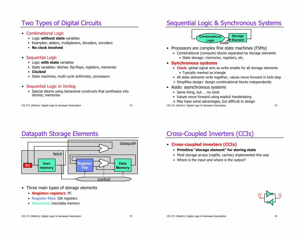
Two Types of Digital Circuits • Combinational Logic
• Logic without state variables • Examples: adders, multiplexers, decoders, encoders • No clock involved
• Sequential Logic • Logic with state variables • State variables: latches, flip-flops, registers, memories • Clocked • State machines, multi-cycle arithmetic, processors
• Sequential Logic in Verilog • Special idioms using behavioral constructs that synthesize into
latches, memories
CIS 371 (Martin): Digital Logic & Hardware Description 74
Sequential Logic & Synchronous Systems
• Processors are complex fine state machines (FSMs) • Combinational (compute) blocks separated by storage elements
• State storage: memories, registers, etc. • Synchronous systems
• Clock: global signal acts as write enable for all storage elements • Typically marked as triangle
• All state elements write together, values move forward in lock-step + Simplifies design: design combinational blocks independently
• Aside: asynchronous systems • Same thing, but … no clock • Values move forward using explicit handshaking ± May have some advantages, but difficult to design
Combinational Logic
Storage Element
Clock
CIS 371 (Martin): Digital Logic & Hardware Description 75
Datapath Storage Elements
• Three main types of storage elements • Singleton registers: PC • Register files: ISA registers • Memories: insn/data memory
PC Insn memory
Register File
Data Memory
control
datapath
fetch
CIS 371 (Martin): Digital Logic & Hardware Description 76
Cross-Coupled Inverters (CCIs)
• Cross-coupled inverters (CCIs) • Primitive “storage element” for storing state • Most storage arrays (regfile, caches) implemented this way • Where is the input and where is the output?
Q’ Q
CIS 371 (Martin): Digital Logic & Hardware Description 77
S-R Latch
• S-R (set-reset) latch • Cross-coupled NOR gates • Distinct inputs/outputs
S,R → Q 0,0 → oldQ 0,1 → 0 1,0 → 1 1,1 → 0
• S=0, R=0? circuit degenerates to cross-coupled INVs • S=1, R=1? not very useful • Not really used … except as component in something else
Q R
S
SR R
S
Q
Q’
CIS 371 (Martin): Digital Logic & Hardware Description 78
D Latch
• D latch: S-R latch + … • control that makes S=R=1 impossible
E,D → Q 0,0 → oldQ 0,1 → oldQ 1,0 → 0 1,1 → 1
• In other words 0,D → oldQ 1,D → D
• In words • When E is 1, Q gets D • When E is 0, Q retains old value
Q
E
D
DL D
E
Q
CIS 371 (Martin): Digital Logic & Hardware Description 79
Timing Diagrams
• Voltage {0,1} diagrams for different nodes in system • “Digitally stylized”: changes are vertical lines (instantaneous?) • Reality is analog, changes are continuous and smooth
• Timing diagram for a D latch
E
D
Q
CIS 371 (Martin): Digital Logic & Hardware Description 80
Triggering: Level vs. Edge
• The D-latch is level-triggered • The latch is open for writing as long as E is 1 • If D changes continuously, so does Q – May not be the functionality we want
• Often easier to reason about an edge-triggered latch • The latch is open for writing only on E transition (0 → 1 or 1 → 0) + Don’t need to worry about fluctuations in value of D
E
D
Q
CIS 371 (Martin): Digital Logic & Hardware Description 81
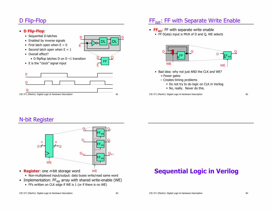
D Flip-Flop
• D Flip-Flop: • Sequential D-latches • Enabled by inverse signals • First latch open when E = 0 • Second latch open when E = 1 • Overall effect?
• D flipflop latches D on 0→1 transition • E is the “clock” signal input
E
D
Q
DL D
E
Q DL
FF D
E
Q
CIS 371 (Martin): Digital Logic & Hardware Description 82
FFWE: FF with Separate Write Enable • FFWE: FF with separate write enable
• FF D(ata) input is MUX of D and Q, WE selects
• Bad idea: why not just AND the CLK and WE? + Fewer gates – Creates timing problems
Do not try to do logic on CLK in Verilog No, really. Never do this.
FFWE D
Q
WE
FF
D Q
WE
CIS 371 (Martin): Digital Logic & Hardware Description 83
N-bit Register
• Register: one n-bit storage word • Non-multiplexed input/output: data buses write/read same word
• Implementation: FFWE array with shared write-enable (WE) • FFs written on CLK edge if WE is 1 (or if there is no WE)
D Q n n
WE
FFWE
FFWE
FFWE
D0
DN-1
D1
WE
Q0
Q1
QN-1
Sequential Logic in Verilog
CIS 371 (Martin): Digital Logic & Hardware Description 84

CIS 371 (Martin): Digital Logic & Hardware Description 85
Designing Sequential Logic
• CIS371 design rule: separate combinational logic from sequential state elements • Not enforced by Verilog, but a very good idea • Possible exceptions: counters, shift registers
• We’ll give you a flip-flop module (see next slide) • Edge-triggered, not a transparent latch • Parameterized to create a n-bit register
• Example use: state machine
Combinational Logic
State Register
Output
Next State
Current State
Clock
CIS 371 (Martin): Digital Logic & Hardware Description 86
Sequential Logic In Verilog
• How are state-holding variables specified in Verilog? • First instinct: structurally • After all, real latches and flip-flops are made from gates…
module latch(out, in, we);!output out; input in, we;!wire not_out = ~(out | (we & ~in));!assign out = ~(not_out | (we & in));!
endmodule !
• This should work, right? RIGHT? • Logically, yes… in practice, no
• Storage elements are highly analog • FPGAs have dedicated storage
we!
in!out!
CIS 371 (Martin): Digital Logic & Hardware Description 87
Verilog Flipflop (Behavioral Magic) • How do we specify state-holding constructs in Verilog? module dff (out, in, wen, rst, clk); !
output out; ! input in; ! input wen, rst, clk; !
reg out; ! always @(posedge clk)! begin! if (rst)! out = 0;! else if (wen)! out = in;! end !endmodule !
wen = write enable rst = reset clk = clock
• reg: interface-less storage bit • always @ (): synthesizable
behavioral sequential Verilog • Tricky: hard to know exactly what it
will synthesize to • We will give this to you,
don’t write your own • “Creativity is a poor substitute for
knowing what you’re doing”!
CIS 371 (Martin): Digital Logic & Hardware Description 88
Verilog Register (Behavioral Magic) • How do we specify state-holding constructs in Verilog? module register (out, in, wen, rst, clk); ! parameter n = 1; ! output [n-1:0] out; ! input [n-1:0] in; ! input wen, rst, clk; !
reg [n-1:0] out; ! always @(posedge clk)! begin! if (rst)! out = 0;! else if (wen)! out = in;! end !endmodule !
wen = write enable rst = reset clk = clock
• reg: interface-less storage bit • always @ (): synthesizable
behavioral sequential Verilog • Tricky: hard to know exactly what it
will synthesize to • We will give this to you,
don’t write your own • “Creativity is a poor substitute for
knowing what you’re doing”!

CIS 371 (Martin): Digital Logic & Hardware Description 89
Clocks Signals • Clocks & reset signals are not normal signals
• Travel on dedicated “clock” wires • Reach all parts of the chip • Special “low-skew” routing
• Ramifications: • Never do logic operations on the clocks • If you want to add a “write enable” to a flip-flop:
• Use a mux to route the old value back into it • (or use the flip-flop with write enable we give you!) • Do not just “and” the write-enable signal with the clock!
• Messing with the clock can cause a errors • Often can only be found using detail low-level simulation
CIS 371 (Martin): Digital Logic & Hardware Description 90
Simulation
• One way to test and debug designs • Graphical output via waveforms
CIS 371 (Martin): Digital Logic & Hardware Description 91
Testbenches
• A more effective way to test & debug designs
• In C/Java? • Write test code in C/Java to test C/Java • “Test harness”, “unit testing”
• For Verilog/VHDL? • Write test code in Verilog to test Verilog • Verilog has advanced “behavioral” commands to facilitate this:
• Delay for n units of time • Full high-level constructs: if, while, sequential assignment, ints • Input/output: file I/O, output to display, etc.
CIS 371 (Martin): Digital Logic & Hardware Description 92
Common Errors
• Tools are from a less gentle time • More like C, less like Java • Assume that you mean what you say
• Common errors: • Not assigning a wire a value • Assigning a wire a value more than once • Implicit wire declarations (default to type “wire” 1-bit wide)
• Avoid names such as: • clock, clk, power, pwr, ground, gnd, vdd, vcc, init, reset, rst • Some of these are “special” and will silently cause errors
CIS 371 (Martin): Digital Logic & Hardware Description 93
Additional Verilog Resources
• Elements of Logic Design Style by Shing Kong, 2001 • Dos, do-nots, tips • http://www.cis.upenn.edu/~milom/elements-of-logic-design-style/
• Verilog HDL Synthesis: A Practical Primer • By J. Bhasker, 1998 • To the point (<200 pages)
• Advanced Digital Design with the Verilog HDL • By Michael D. Ciletti, 2003 • Verilog plus lots of digital logic design (~1000 pages)
• Verilog tutorial from textbook (posted on course web page)
CIS 371 (Martin): Digital Logic & Hardware Description 94
• Transistors & frabrication • Digital logic basics
• Focus on useful components
• Hardware design methods • Introduction to Verilog
• Next unit: single-cycle datapath
CPU Mem I/O
System software
App App App
Summary

![ENSC427:CommunicationNetworks,Spring2012 ... › ~ljilja › ENSC427 › Spring12 › Projects › team12 › ENSC...References’! [1]A.Zaballos,G.Corral,I.Serra,J.Abella,"TestingNetworkSecurity%](https://img.pdfslide.net/doc/110x75/5f0ec6637e708231d440e03f/ensc427communicationnetworksspring2012-a-ljilja-a-ensc427-a-spring12.jpg)


![[Www.uobstudy.com] MATH 270 Spring12 Exam1](https://img.pdfslide.net/doc/110x75/56d6bf9a1a28ab301696e2fe/wwwuobstudycom-math-270-spring12-exam1.jpg)