Embed Size (px)
Citation preview

Three-Dimensional Morphology andCrystallography of Gold NanorodsHadas Katz-Boon,† Chris J. Rossouw,‡ Matthew Weyland,†,‡ Alison M. Funston,§,|
Paul Mulvaney,§ and Joanne Etheridge*,†,‡
Department of Materials Engineering and Monash Centre for Electron Microscopy, Monash University,Victoria 3800, Australia, and School of Chemistry and Bio21 Institute, University of Melbourne,Parkville, VIC, 3010, Australia
ABSTRACT We determine the three-dimensional shape, to within 1 nm resolution, of single-crystal gold nanorods grown in thepresence of silver ions using electron tomography and thickness profile measurements. We find that, contrary to the current literature,the octagonal side-facets are sparsely packed atomic planes all belonging to the same symmetry-equivalent family, {0 5 12}.Furthermore, the rod ends terminate in a pyramid with slightly different facets, and each pyramid is connected to the sides by foursmall {0 5 12} “bridging” facets.
KEYWORDS Gold nanorods, gold nanostructure, crystal growth, electron microscopy, electron tomography, scanningtransmission electron microscopy
Understanding the mechanisms that determine crys-tal morphology is a major challenge in materialsscience.1-4 Since the ground-breaking demonstra-
tion of nanocrystal shape control via surfactant templating,5
gold nanorods have become the model system for under-standing the growth of highly anisotropic, thermodynami-cally unexpected shapes.6-9 These nanocrystals exhibit avariety of properties, which are exquisitely sensitive toshape, such as the optical response.6,10,11 This has drivenan intense effort over the past decade to understand andcontrol their morphology.7,12,13
Theoretical studies of morphology14 and current modelsof growth mechanisms15,16 and shape transformations17,18
are underpinned by a consensus that gold nanorods, grownin the presence of silver ions, are bound by the same facetsas bulk gold, namely, the closely packed atomic planes:{1 0 0}, {1 1 0}, or {1 1 1} facets.17,19-21 Specifically, thecurrent morphological model describes these nanorods asan octagon formed by four {0 0 1} and four {0 1 1} side-facets and terminated by {1 0 0}, {1 1 0}, or {1 1 1}facets.17,19-21 The growth of a rod-like shape implies thatthe rod ends grow at a faster rate than the sides,20 so theidentification of the rod end-facets and some of the side-facets as belonging to the same {1 0 0} family has beenproblematic. It is difficult to understand why the rods growpreferentially along only one of the three symmetry-
equivalent ⟨1 0 0⟩ directions. Similarly, it is difficult tounderstand why the octagon should have side-facets belong-ing to symmetry-inequivalent atomic planes, which mightbe expected to have different surface energies.
Transmission electron microscopy (TEM) has been usedto analyze nanorod morphology; however, it is difficult toobtain quantitative information about the specimen in thethird dimension using conventional methods. For example,a single-atomic-resolution TEM image permits the identifica-tion of only a vector parallel to the facet plane. Images inseveral different projections are required to determine theorientation of the plane itself.22,23
Here we have undertaken an analysis of the three-dimensional shape (3D) and crystallography of gold nano-rods using scanning transmission electron microscope (STEM)images acquired with a high-angle annular dark field (HAADF)detector. We have derived complementary 3D informationfrom these images using two methods: HAADF-STEM to-mography24 and a novel HAADF-STEM “thickness profile”method.25
In HAADF-STEM, a focused electron beam is scannedacross the specimen and at each point in the scan theelectrons scattered to high angles are counted by an annulardetector. The result is a two-dimensional (2D) “image” ofintensity versus specimen position. The intensity has amonotonic dependence on specimen thickness (for thick-nesses in the range considered here),26-29 making it suitablefor both the tomography and thickness profile methods.
HAADF-STEM tomography24 enables the reconstructionof 3D shapes from a sequence of 2D images taken atdifferent specimen orientations. Figure 1a-c shows a mon-tage of images of the 3D morphology of a single goldnanorod, determined from a tomographic reconstructionand displayed as a surface rendering. (A movie is provided
* Corresponding author: [email protected].† Department of Materials Engineering, Monash University.‡ Monash Centre for Electron Microscopy, Monash University.| School of Chemistry, Monash University.§ University of Melbourne.Received for review: 10/23/2010Published on Web: 12/23/2010
pubs.acs.org/NanoLett
© 2011 American Chemical Society 273 DOI: 10.1021/nl103726k | Nano Lett. 2011, 11, 273–278
in the Supporting Information.) The image series was ac-quired using an ultrastable high-resolution instrument andoperating environment30 so that the reconstruction has aspatial resolution of better than 1 nm.31
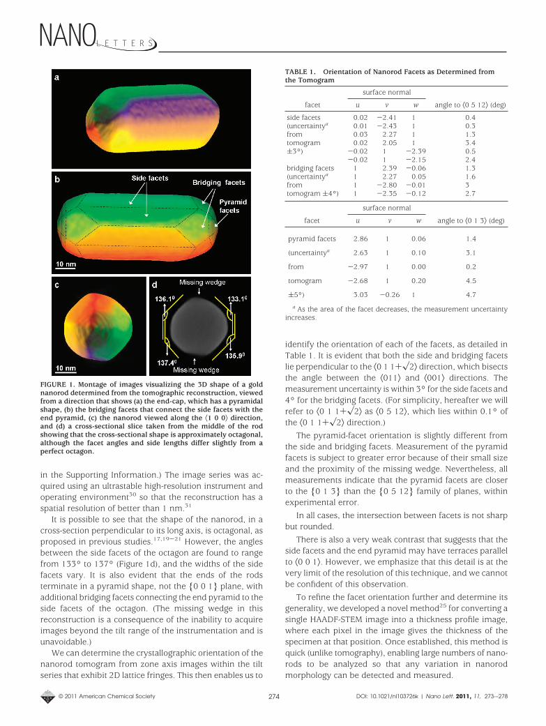
It is possible to see that the shape of the nanorod, in across-section perpendicular to its long axis, is octagonal, asproposed in previous studies.17,19-21 However, the anglesbetween the side facets of the octagon are found to rangefrom 133° to 137° (Figure 1d), and the widths of the sidefacets vary. It is also evident that the ends of the rodsterminate in a pyramid shape, not the {0 0 1} plane, withadditional bridging facets connecting the end pyramid to theside facets of the octagon. (The missing wedge in thisreconstruction is a consequence of the inability to acquireimages beyond the tilt range of the instrumentation and isunavoidable.)
We can determine the crystallographic orientation of thenanorod tomogram from zone axis images within the tiltseries that exhibit 2D lattice fringes. This then enables us to
identify the orientation of each of the facets, as detailed inTable 1. It is evident that both the side and bridging facetslie perpendicular to the ⟨0 1 1+�2⟩ direction, which bisectsthe angle between the ⟨011⟩ and ⟨001⟩ directions. Themeasurement uncertainty is within 3° for the side facets and4° for the bridging facets. (For simplicity, hereafter we willrefer to ⟨0 1 1+�2⟩ as ⟨0 5 12⟩, which lies within 0.1° ofthe ⟨0 1 1+�2⟩ direction.)
The pyramid-facet orientation is slightly different fromthe side and bridging facets. Measurement of the pyramidfacets is subject to greater error because of their small sizeand the proximity of the missing wedge. Nevertheless, allmeasurements indicate that the pyramid facets are closerto the {0 1 3} than the {0 5 12} family of planes, withinexperimental error.
In all cases, the intersection between facets is not sharpbut rounded.
There is also a very weak contrast that suggests that theside facets and the end pyramid may have terraces parallelto ⟨0 0 1⟩. However, we emphasize that this detail is at thevery limit of the resolution of this technique, and we cannotbe confident of this observation.
To refine the facet orientation further and determine itsgenerality, we developed a novel method25 for converting asingle HAADF-STEM image into a thickness profile image,where each pixel in the image gives the thickness of thespecimen at that position. Once established, this method isquick (unlike tomography), enabling large numbers of nano-rods to be analyzed so that any variation in nanorodmorphology can be detected and measured.
FIGURE 1. Montage of images visualizing the 3D shape of a goldnanorod determined from the tomographic reconstruction, viewedfrom a direction that shows (a) the end-cap, which has a pyramidalshape, (b) the bridging facets that connect the side facets with theend pyramid, (c) the nanorod viewed along the ⟨1 0 0⟩ direction,and (d) a cross-sectional slice taken from the middle of the rodshowing that the cross-sectional shape is approximately octagonal,although the facet angles and side lengths differ slightly from aperfect octagon.
TABLE 1. Orientation of Nanorod Facets as Determined fromthe Tomogram
surface normal
facet u v w angle to ⟨0 5 12⟩ (deg)
side facets 0.02 -2.41 1 0.4(uncertaintya 0.01 -2.43 1 0.3from 0.03 2.27 1 1.3tomogram 0.02 2.05 1 3.4(3°) -0.02 1 -2.39 0.5
-0.02 1 -2.15 2.4bridging facets 1 2.39 -0.06 1.3(uncertaintya 1 2.27 0.05 1.6from 1 -2.80 -0.01 3tomogram (4°) 1 -2.35 -0.12 2.7
surface normal
facet u v w angle to ⟨0 1 3⟩ (deg)
pyramid facets 2.86 1 0.06 1.4
(uncertaintya 2.63 1 0.10 3.1
from -2.97 1 0.00 0.2
tomogram -2.68 1 0.20 4.5
(5°) 3.03 -0.26 1 4.7
a As the area of the facet decreases, the measurement uncertaintyincreases.
© 2011 American Chemical Society 274 DOI: 10.1021/nl103726k | Nano Lett. 2011, 11, 273-–278
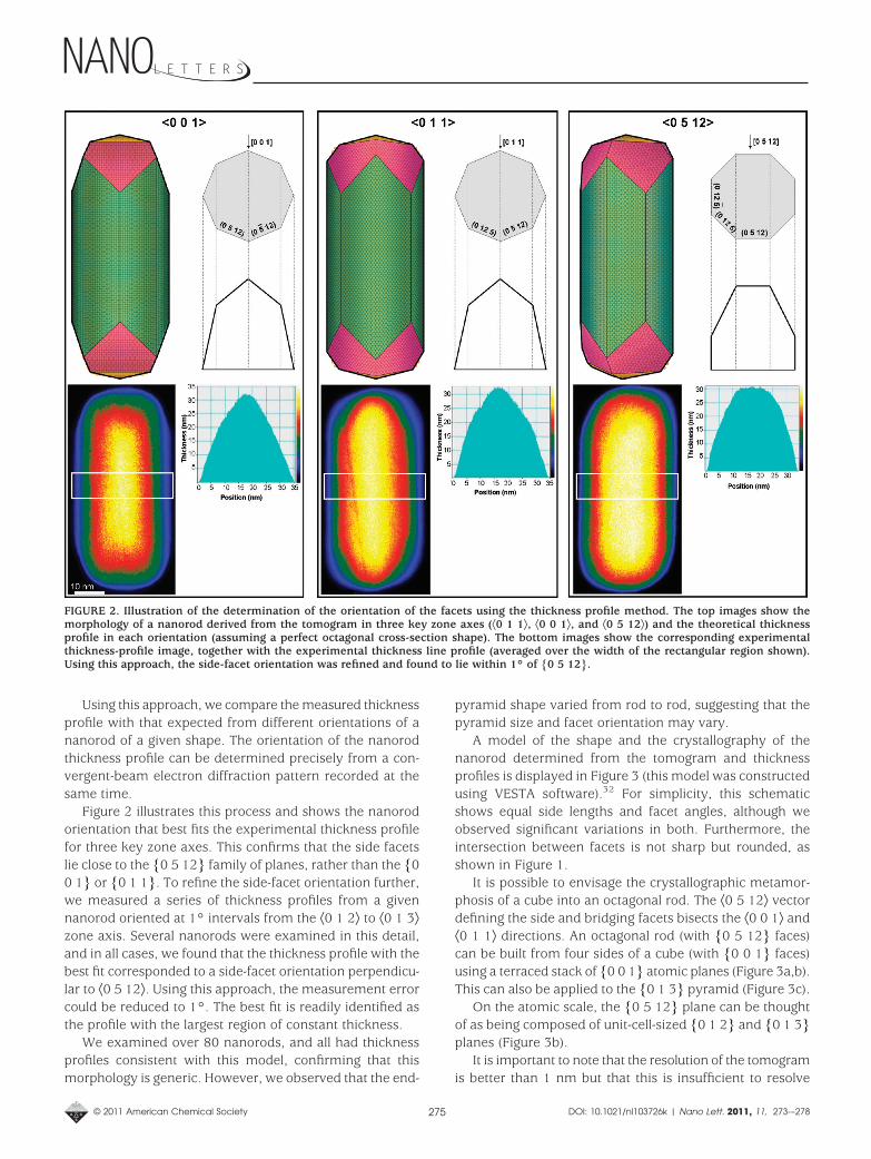
Using this approach, we compare the measured thicknessprofile with that expected from different orientations of ananorod of a given shape. The orientation of the nanorodthickness profile can be determined precisely from a con-vergent-beam electron diffraction pattern recorded at thesame time.
Figure 2 illustrates this process and shows the nanorodorientation that best fits the experimental thickness profilefor three key zone axes. This confirms that the side facetslie close to the {0 5 12} family of planes, rather than the {00 1} or {0 1 1}. To refine the side-facet orientation further,we measured a series of thickness profiles from a givennanorod oriented at 1° intervals from the ⟨0 1 2⟩ to ⟨0 1 3⟩zone axis. Several nanorods were examined in this detail,and in all cases, we found that the thickness profile with thebest fit corresponded to a side-facet orientation perpendicu-lar to ⟨0 5 12⟩. Using this approach, the measurement errorcould be reduced to 1°. The best fit is readily identified asthe profile with the largest region of constant thickness.
We examined over 80 nanorods, and all had thicknessprofiles consistent with this model, confirming that thismorphology is generic. However, we observed that the end-
pyramid shape varied from rod to rod, suggesting that thepyramid size and facet orientation may vary.
A model of the shape and the crystallography of thenanorod determined from the tomogram and thicknessprofiles is displayed in Figure 3 (this model was constructedusing VESTA software).32 For simplicity, this schematicshows equal side lengths and facet angles, although weobserved significant variations in both. Furthermore, theintersection between facets is not sharp but rounded, asshown in Figure 1.
It is possible to envisage the crystallographic metamor-phosis of a cube into an octagonal rod. The ⟨0 5 12⟩ vectordefining the side and bridging facets bisects the ⟨0 0 1⟩ and⟨0 1 1⟩ directions. An octagonal rod (with {0 5 12} faces)can be built from four sides of a cube (with {0 0 1} faces)using a terraced stack of {0 0 1} atomic planes (Figure 3a,b).This can also be applied to the {0 1 3} pyramid (Figure 3c).
On the atomic scale, the {0 5 12} plane can be thoughtof as being composed of unit-cell-sized {0 1 2} and {0 1 3}planes (Figure 3b).
It is important to note that the resolution of the tomogramis better than 1 nm but that this is insufficient to resolve
FIGURE 2. Illustration of the determination of the orientation of the facets using the thickness profile method. The top images show themorphology of a nanorod derived from the tomogram in three key zone axes (⟨0 1 1⟩, ⟨0 0 1⟩, and ⟨0 5 12⟩) and the theoretical thicknessprofile in each orientation (assuming a perfect octagonal cross-section shape). The bottom images show the corresponding experimentalthickness-profile image, together with the experimental thickness line profile (averaged over the width of the rectangular region shown).Using this approach, the side-facet orientation was refined and found to lie within 1° of {0 5 12}.
© 2011 American Chemical Society 275 DOI: 10.1021/nl103726k | Nano Lett. 2011, 11, 273-–278
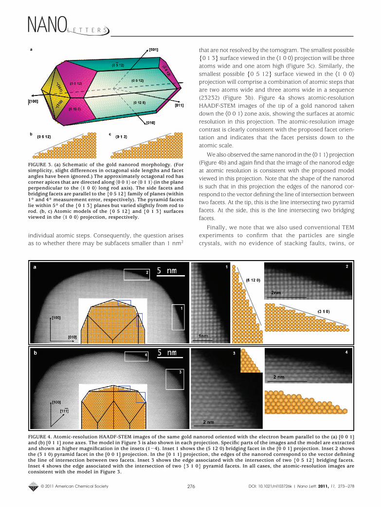
individual atomic steps. Consequently, the question arisesas to whether there may be subfacets smaller than 1 nm2
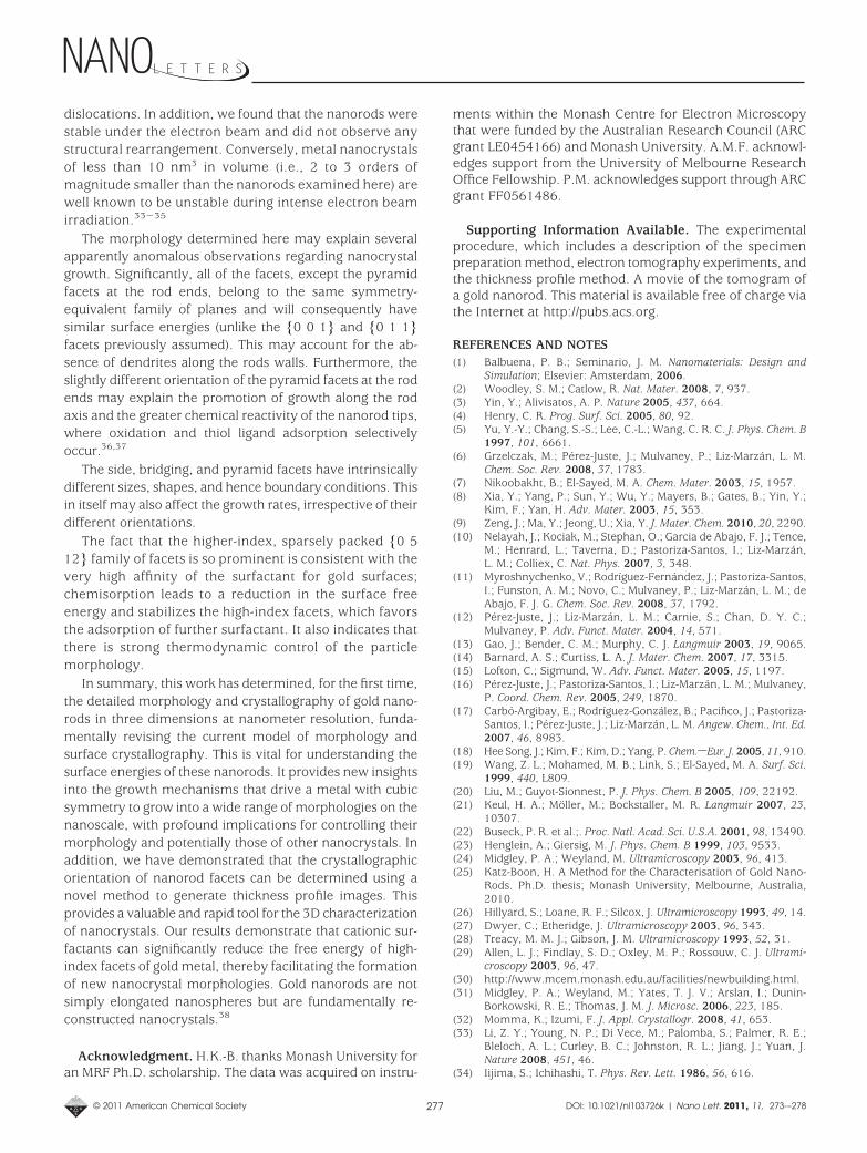
that are not resolved by the tomogram. The smallest possible{0 1 3} surface viewed in the ⟨1 0 0⟩ projection will be threeatoms wide and one atom high (Figure 3c). Similarly, thesmallest possible {0 5 12} surface viewed in the ⟨1 0 0⟩projection will comprise a combination of atomic steps thatare two atoms wide and three atoms wide in a sequence(23232) (Figure 3b). Figure 4a shows atomic-resolutionHAADF-STEM images of the tip of a gold nanorod takendown the ⟨0 0 1⟩ zone axis, showing the surfaces at atomicresolution in this projection. The atomic-resolution imagecontrast is clearly consistent with the proposed facet orien-tation and indicates that the facet persists down to theatomic scale.
We also observed the same nanorod in the ⟨0 1 1⟩ projection(Figure 4b) and again find that the image of the nanorod edgeat atomic resolution is consistent with the proposed modelviewed in this projection. Note that the shape of the nanorodis such that in this projection the edges of the nanorod cor-respond to the vector defining the line of intersection betweentwo facets. At the tip, this is the line intersecting two pyramidfacets. At the side, this is the line intersecting two bridgingfacets.
Finally, we note that we also used conventional TEMexperiments to confirm that the particles are singlecrystals, with no evidence of stacking faults, twins, or
FIGURE 4. Atomic-resolution HAADF-STEM images of the same gold nanorod oriented with the electron beam parallel to the (a) [0 0 1]and (b) [0 1 1] zone axes. The model in Figure 3 is also shown in each projection. Specific parts of the images and the model are extractedand shown at higher magnification in the insets (1-4). Inset 1 shows the (5 12 0) bridging facet in the [0 0 1] projection. Inset 2 showsthe (3 1 0) pyramid facet in the [0 0 1] projection. In the [0 1 1] projection, the edges of the nanorod correspond to the vector definingthe line of intersection between two facets. Inset 3 shows the edge associated with the intersection of two {0 5 12} bridging facets.Inset 4 shows the edge associated with the intersection of two {3 1 0} pyramid facets. In all cases, the atomic-resolution images areconsistent with the model in Figure 3.
FIGURE 3. (a) Schematic of the gold nanorod morphology. (Forsimplicity, slight differences in octagonal side lengths and facetangles have been ignored.) The approximately octagonal rod hascorner apices that are directed along ⟨0 0 1⟩ or ⟨0 1 1⟩ (in the planeperpendicular to the ⟨1 0 0⟩ long rod axis). The side facets andbridging facets are parallel to the {0 5 12} family of planes (within1° and 4° measurement error, respectively). The pyramid facetslie within 5° of the {0 1 3} planes but varied slightly from rod torod. (b, c) Atomic models of the {0 5 12} and {0 1 3} surfacesviewed in the ⟨1 0 0⟩ projection, respectively.
© 2011 American Chemical Society 276 DOI: 10.1021/nl103726k | Nano Lett. 2011, 11, 273-–278
dislocations. In addition, we found that the nanorods werestable under the electron beam and did not observe anystructural rearrangement. Conversely, metal nanocrystalsof less than 10 nm3 in volume (i.e., 2 to 3 orders ofmagnitude smaller than the nanorods examined here) arewell known to be unstable during intense electron beamirradiation.33-35
The morphology determined here may explain severalapparently anomalous observations regarding nanocrystalgrowth. Significantly, all of the facets, except the pyramidfacets at the rod ends, belong to the same symmetry-equivalent family of planes and will consequently havesimilar surface energies (unlike the {0 0 1} and {0 1 1}facets previously assumed). This may account for the ab-sence of dendrites along the rods walls. Furthermore, theslightly different orientation of the pyramid facets at the rodends may explain the promotion of growth along the rodaxis and the greater chemical reactivity of the nanorod tips,where oxidation and thiol ligand adsorption selectivelyoccur.36,37
The side, bridging, and pyramid facets have intrinsicallydifferent sizes, shapes, and hence boundary conditions. Thisin itself may also affect the growth rates, irrespective of theirdifferent orientations.
The fact that the higher-index, sparsely packed {0 512} family of facets is so prominent is consistent with thevery high affinity of the surfactant for gold surfaces;chemisorption leads to a reduction in the surface freeenergy and stabilizes the high-index facets, which favorsthe adsorption of further surfactant. It also indicates thatthere is strong thermodynamic control of the particlemorphology.
In summary, this work has determined, for the first time,the detailed morphology and crystallography of gold nano-rods in three dimensions at nanometer resolution, funda-mentally revising the current model of morphology andsurface crystallography. This is vital for understanding thesurface energies of these nanorods. It provides new insightsinto the growth mechanisms that drive a metal with cubicsymmetry to grow into a wide range of morphologies on thenanoscale, with profound implications for controlling theirmorphology and potentially those of other nanocrystals. Inaddition, we have demonstrated that the crystallographicorientation of nanorod facets can be determined using anovel method to generate thickness profile images. Thisprovides a valuable and rapid tool for the 3D characterizationof nanocrystals. Our results demonstrate that cationic sur-factants can significantly reduce the free energy of high-index facets of gold metal, thereby facilitating the formationof new nanocrystal morphologies. Gold nanorods are notsimply elongated nanospheres but are fundamentally re-constructed nanocrystals.38
Acknowledgment. H.K.-B. thanks Monash University foran MRF Ph.D. scholarship. The data was acquired on instru-
ments within the Monash Centre for Electron Microscopythat were funded by the Australian Research Council (ARCgrant LE0454166) and Monash University. A.M.F. acknowl-edges support from the University of Melbourne ResearchOffice Fellowship. P.M. acknowledges support through ARCgrant FF0561486.
Supporting Information Available. The experimentalprocedure, which includes a description of the specimenpreparation method, electron tomography experiments, andthe thickness profile method. A movie of the tomogram ofa gold nanorod. This material is available free of charge viathe Internet at http://pubs.acs.org.
REFERENCES AND NOTES(1) Balbuena, P. B.; Seminario, J. M. Nanomaterials: Design and
Simulation; Elsevier: Amsterdam, 2006.(2) Woodley, S. M.; Catlow, R. Nat. Mater. 2008, 7, 937.(3) Yin, Y.; Alivisatos, A. P. Nature 2005, 437, 664.(4) Henry, C. R. Prog. Surf. Sci. 2005, 80, 92.(5) Yu, Y.-Y.; Chang, S.-S.; Lee, C.-L.; Wang, C. R. C. J. Phys. Chem. B
1997, 101, 6661.(6) Grzelczak, M.; Perez-Juste, J.; Mulvaney, P.; Liz-Marzan, L. M.
Chem. Soc. Rev. 2008, 37, 1783.(7) Nikoobakht, B.; El-Sayed, M. A. Chem. Mater. 2003, 15, 1957.(8) Xia, Y.; Yang, P.; Sun, Y.; Wu, Y.; Mayers, B.; Gates, B.; Yin, Y.;
Kim, F.; Yan, H. Adv. Mater. 2003, 15, 353.(9) Zeng, J.; Ma, Y.; Jeong, U.; Xia, Y. J. Mater. Chem. 2010, 20, 2290.(10) Nelayah, J.; Kociak, M.; Stephan, O.; Garcia de Abajo, F. J.; Tence,
M.; Henrard, L.; Taverna, D.; Pastoriza-Santos, I.; Liz-Marzan,L. M.; Colliex, C. Nat. Phys. 2007, 3, 348.
(11) Myroshnychenko, V.; Rodrıguez-Fernandez, J.; Pastoriza-Santos,I.; Funston, A. M.; Novo, C.; Mulvaney, P.; Liz-Marzan, L. M.; deAbajo, F. J. G. Chem. Soc. Rev. 2008, 37, 1792.
(12) Perez-Juste, J.; Liz-Marzan, L. M.; Carnie, S.; Chan, D. Y. C.;Mulvaney, P. Adv. Funct. Mater. 2004, 14, 571.
(13) Gao, J.; Bender, C. M.; Murphy, C. J. Langmuir 2003, 19, 9065.(14) Barnard, A. S.; Curtiss, L. A. J. Mater. Chem. 2007, 17, 3315.(15) Lofton, C.; Sigmund, W. Adv. Funct. Mater. 2005, 15, 1197.(16) Perez-Juste, J.; Pastoriza-Santos, I.; Liz-Marzan, L. M.; Mulvaney,
P. Coord. Chem. Rev. 2005, 249, 1870.(17) Carbó-Argibay, E.; Rodrıguez-Gonzalez, B.; Pacifico, J.; Pastoriza-
Santos, I.; Perez-Juste, J.; Liz-Marzan, L. M. Angew. Chem., Int. Ed.2007, 46, 8983.
(18) Hee Song, J.; Kim, F.; Kim, D.; Yang, P. Chem.sEur. J. 2005, 11, 910.(19) Wang, Z. L.; Mohamed, M. B.; Link, S.; El-Sayed, M. A. Surf. Sci.
1999, 440, L809.(20) Liu, M.; Guyot-Sionnest, P. J. Phys. Chem. B 2005, 109, 22192.(21) Keul, H. A.; Möller, M.; Bockstaller, M. R. Langmuir 2007, 23,
10307.(22) Buseck, P. R. et al.;. Proc. Natl. Acad. Sci. U.S.A. 2001, 98, 13490.(23) Henglein, A.; Giersig, M. J. Phys. Chem. B 1999, 103, 9533.(24) Midgley, P. A.; Weyland, M. Ultramicroscopy 2003, 96, 413.(25) Katz-Boon, H. A Method for the Characterisation of Gold Nano-
Rods. Ph.D. thesis; Monash University, Melbourne, Australia,2010.
(26) Hillyard, S.; Loane, R. F.; Silcox, J. Ultramicroscopy 1993, 49, 14.(27) Dwyer, C.; Etheridge, J. Ultramicroscopy 2003, 96, 343.(28) Treacy, M. M. J.; Gibson, J. M. Ultramicroscopy 1993, 52, 31.(29) Allen, L. J.; Findlay, S. D.; Oxley, M. P.; Rossouw, C. J. Ultrami-
croscopy 2003, 96, 47.(30) http://www.mcem.monash.edu.au/facilities/newbuilding.html.(31) Midgley, P. A.; Weyland, M.; Yates, T. J. V.; Arslan, I.; Dunin-
Borkowski, R. E.; Thomas, J. M. J. Microsc. 2006, 223, 185.(32) Momma, K.; Izumi, F. J. Appl. Crystallogr. 2008, 41, 653.(33) Li, Z. Y.; Young, N. P.; Di Vece, M.; Palomba, S.; Palmer, R. E.;
Bleloch, A. L.; Curley, B. C.; Johnston, R. L.; Jiang, J.; Yuan, J.Nature 2008, 451, 46.
(34) Iijima, S.; Ichihashi, T. Phys. Rev. Lett. 1986, 56, 616.
© 2011 American Chemical Society 277 DOI: 10.1021/nl103726k | Nano Lett. 2011, 11, 273-–278
(35) Ajayan, P. M.; Marks, L. D. Phys. Rev. Lett. 1989, 63, 279.(36) Rodrıguez-Fernandez, J.; Perez-Juste, J.; Mulvaney, P.; Liz-Marzan,
L. M. J. Phys. Chem. B 2005, 109, 14257.(37) Thomas, K. G.; Barazzouk, S.; Ipe, B. I.; Joseph, S. T. S.; Kamat,
P. V. J. Phys Chem B 2004, 108, 13066.(38) During the processing of this manuscript, a related paper has been
brought to our attention, which is in close agreement with ourmain conclusions: Carbo-Argibay, E.; Rodrıguez-Gonzalez, B.;
Gomez-Graña, S.; Guerrero-Martınez, A.; Pastoriza-Santos, I.;Perez-Juste, J.; Liz-Marzan, L. M. Angew. Chem. Int. Ed. 2010, 49,9397.
(39) Gilbert, P. J. Theor. Biol. 1972, 36, 105.(40) http://www.amira.com/.(41) Rossouw, C. J. Ultramicroscopy 1995, 58, 211.(42) Rossouw, C. J.; Allen, L. J.; Findlay, S. D.; Oxley, M. P. Ultrami-
croscopy 2003, 96, 299.
© 2011 American Chemical Society 278 DOI: 10.1021/nl103726k | Nano Lett. 2011, 11, 273-–278