Embed Size (px)
Citation preview
Journal of Modern Physics, 2012, 3, 856-864 http://dx.doi.org/10.4236/jmp.2012.38112 Published Online August 2012 (http://www.SciRP.org/journal/jmp)
Three-Photon Absorption in ZnO Film Using Ultra Short Pulse Laser
Raied K. Jamal, Mohammed T. Hussein, Abdulla M. Suhail Department of Physics, College of Science, University of Baghdad, Baghdad, Iraq
Email: [email protected], [email protected], [email protected], [email protected]
Received January 4, 2012; revised February 1, 2012; accepted February 27, 2012
ABSTRACT
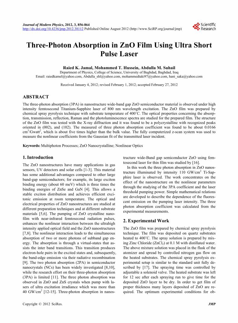
The three-photon absorption (3PA) in nanostructure wide-band gap ZnO semiconductor material is observed under high intensity femtosecond Titanium-Sapphire laser of 800 nm wavelength excitation. The ZnO film was prepared by chemical spray pyrolysis technique with substrate temperature of 400˚C. The optical properties concerning the absorp-tion, transmission, reflection, Raman and the photoluminescence spectra are studied for the prepared film. The structure of the ZnO film was tested with the X-ray diffraction and it was found to be a polycrystalline with recognized peaks oriented in (002), and (102). The measured of three photon absorption coefficient was found to be about 0.0166 cm3/Gwatt2, which is about five times higher than the bulk value. The fully computerized z-scan system was used to measure the nonlinear coefficients from the Gaussian fit of the transmitted laser incident. Keywords: Multiphoton Processes; ZnO Nanocrystalline; Nonlinear Optics
1. Introduction
The ZnO nanostructures have many applications in gas sensors, UV detectors and solar cells [1-3]. This material has some additional advantages compared to other large band-gap semiconductors; for example, its large exciton binding energy (about 60 meV) which is three times the binding energies of ZnSe and GaN [4]. This allows a stable exciton distribution and achieves efficient exci-tonic emission at room temperature. The optical and electrical properties of ZnO nanostructures are studied at different preparation techniques and at different substrate materials [5,6]. The pumping of ZnO crystalline nano-film with near-infrared femtosecond radiation pulses, enhances the nonlinear interaction between the ultrahigh intensity applied optical field and the ZnO nanostructures [7,8]. The nonlinear interaction leads to the simultaneous absorption of two or more photons of subband gap en-ergy. The absorption is through a virtual-states that as-sists the inter band transitions. This transition produces electron-hole pairs in the excited states and, subsequently, the band-edge emission via their radiative recombination [9]. The two photon absorption (2PA) in semiconductor nanocrystals (NCs) has been widely investigated [8,10], while the research effort on their three-photon absorption (3PA) is limited [11]. The three photon absorption was observed in ZnO and ZnS crystals when pump with la-sers of ultra excitation irradiance which was more than 40 GW/cm2 [12-15]. Three-photon absorption in nanos-
tructure wide-Band gap semiconductor ZnO using fem-tosecond laser for thin film was studied by [16].
In this work the three photon absorption in ZnO nanos-tructure illuminated by intensity 110 GW/cm2 Ti-Sap-phire laser is observed. The work concentrates on the effect of the nanostructure on the nonlinear parameters through the studying of the 3PA coefficient and the laser threshold pumping power. Simple mathematical relations are developed to describe the dependence of the fluores-cent emission on the pumping laser intensity. The three photon absorption coefficient was calculated from the experimental measurements.
2. Experimental Work
The ZnO film was prepared by chemical spray pyrolysis technique. The film was deposited on quartz substrates heated to 400˚C. The spray solution is prepared by mix-ing Zinc Chloride (ZnCl2) at 0.1 M with distillated water. The above mixture solution was placed in the flask of the atomizer and spread by controlled nitrogen gas flow on the heated substrates. The chemical spray pyrolysis ex-perimental setup is similar to the standard unit fully de-scribed by [17]. The spraying time was controlled by adjustable a solenoid valve. The heated substrate was left for 12 sec after each spraying run to give time for the deposited ZnO layer to be dry. In order to get film of proper thickness many layers deposited of ZnO are re-quired. The optimum experimental conditions for ob-
Copyright © 2012 SciRes. JMP
R. K. JAMAL ET AL. 857
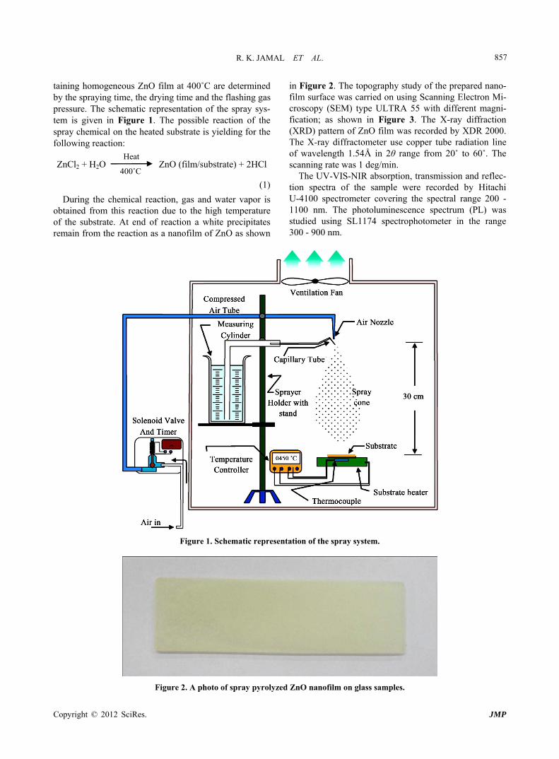
taining homogeneous ZnO film at 400˚C are determined by the spraying time, the drying time and the flashing gas pressure. The schematic representation of the spray sys-tem is given in Figure 1. The possible reaction of the spray chemical on the heated substrate is yielding for the following reaction:
ZnCl2 + H2O Heat
400˚C ZnO (film/substrate) + 2HCl
(1)
During the chemical reaction, gas and water vapor is obtained from this reaction due to the high temperature of the substrate. At end of reaction a white precipitates remain from the reaction as a nanofilm of ZnO as shown
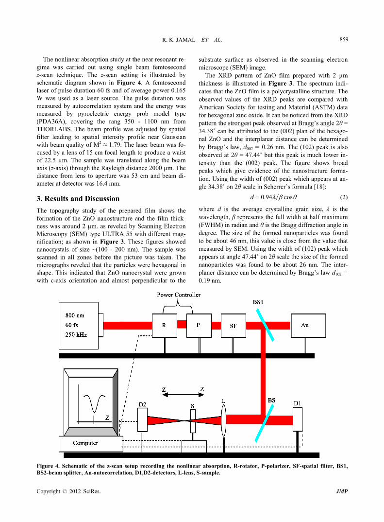
in Figure 2. The topography study of the prepared nano-film surface was carried on using Scanning Electron Mi-croscopy (SEM) type ULTRA 55 with different magni-fication; as shown in Figure 3. The X-ray diffraction (XRD) pattern of ZnO film was recorded by XDR 2000. The X-ray diffractometer use copper tube radiation line of wavelength 1.54Å in 2θ range from 20˚ to 60˚. The scanning rate was 1 deg/min.
The UV-VIS-NIR absorption, transmission and reflec- tion spectra of the sample were recorded by Hitachi U-4100 spectrometer covering the spectral range 200 - 1100 nm. The photoluminescence spectrum (PL) was studied using SL1174 spectrophotometer in the range 300 - 900 nm.
Figure 1. Schematic representation of the spray system.
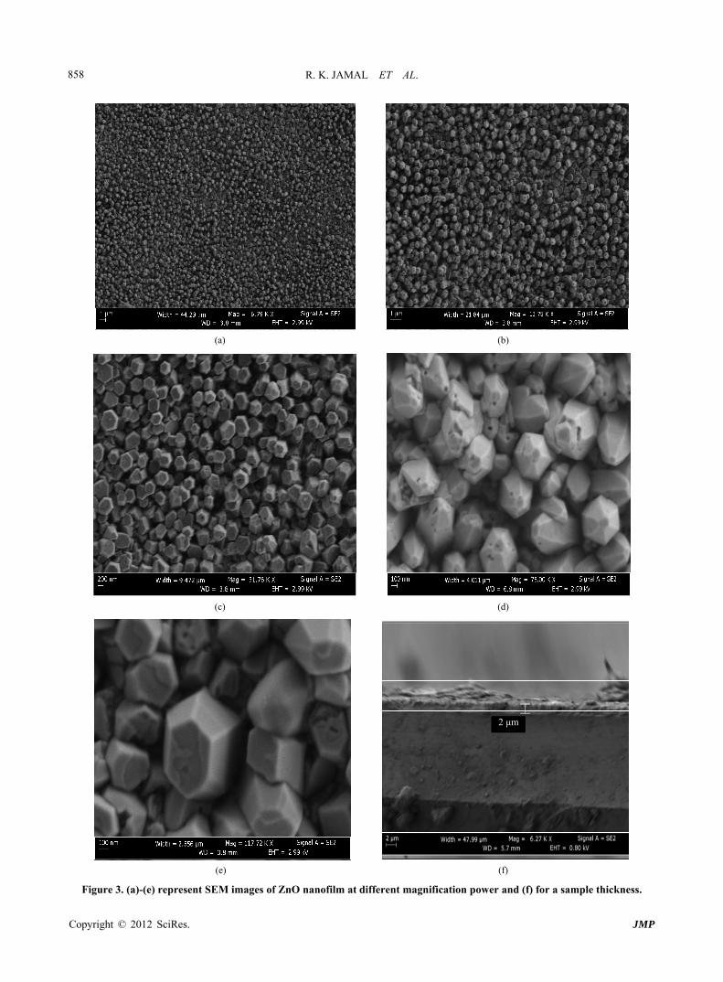
Figure 2. A photo of spray pyrolyzed ZnO nanofilm on glass samples.
Copyright © 2012 SciRes. JMP
R. K. JAMAL ET AL. 858
(a) (b)
(c) (d)
2 μm
(e) (f)
Figure 3. (a)-(e) represent SEM images of ZnO nanofilm at different magnification power and (f) for a sample thickness.
Copyright © 2012 SciRes. JMP
R. K. JAMAL ET AL.
Copyright © 2012 SciRes. JMP
859
The nonlinear absorption study at the near resonant re-
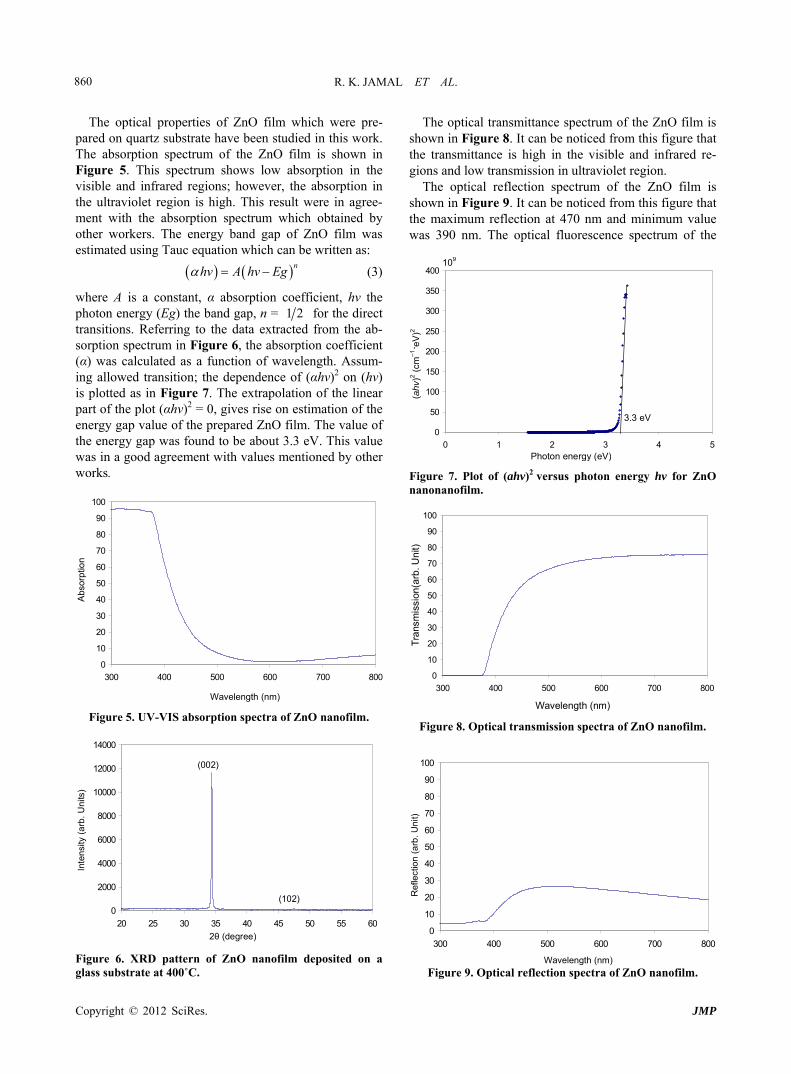
gime was carried out using single beam femtosecond z-scan technique. The z-scan setting is illustrated by schematic diagram shown in Figure 4. A femtosecond laser of pulse duration 60 fs and of average power 0.165 W was used as a laser source. The pulse duration was measured by autocorrelation system and the energy was measured by pyroelectric energy prob model type (PDA36A), covering the rang 350 - 1100 nm from THORLABS. The beam profile was adjusted by spatial filter leading to spatial intensity profile near Gaussian with beam quality of M2 ≈ 1.79. The laser beam was fo-cused by a lens of 15 cm focal length to produce a waist of 22.5 µm. The sample was translated along the beam axis (z-axis) through the Rayleigh distance 2000 µm. The distance from lens to aperture was 53 cm and beam di-ameter at detector was 16.4 mm.
substrate surface as observed in the scanning electron microscope (SEM) image.
The XRD pattern of ZnO film prepared with 2 µm thickness is illustrated in Figure 3. The spectrum indi-cates that the ZnO film is a polycrystalline structure. The observed values of the XRD peaks are compared with American Society for testing and Material (ASTM) data for hexagonal zinc oxide. It can be noticed from the XRD pattern the strongest peak observed at Bragg’s angle 2θ = 34.38˚ can be attributed to the (002) plan of the hexago-nal ZnO and the interplanar distance can be determined by Bragg’s law, d002 = 0.26 nm. The (102) peak is also observed at 2θ = 47.44˚ but this peak is much lower in-tensity than the (002) peak. The figure shows broad peaks which give evidence of the nanostructure forma-tion. Using the width of (002) peak which appears at an-gle 34.38˚ on 2θ scale in Scherrer’s formula [18]:
3. Results and Discussion
The topography study of the prepared film shows the formation of the ZnO nanostructure and the film thick-ness was around 2 µm. as reveled by Scanning Electron Microscopy (SEM) type ULTRA 55 with different mag-nification; as shown in Figure 3. These figures showed nanocrystals of size ~(100 - 200 nm). The sample was scanned in all zones before the picture was taken. The micrographs reveled that the particles were hexagonal in shape. This indicated that ZnO nanocrystal were grown with c-axis orientation and almost perpendicular to the
0.94 cosd (2)
where d is the average crystalline grain size, λ is the wavelength, β represents the full width at half maximum (FWHM) in radian and θ is the Bragg diffraction angle in degree. The size of the formed nanoparticles was found to be about 46 nm, this value is close from the value that measured by SEM. Using the width of (102) peak which appears at angle 47.44˚ on 2θ scale the size of the formed nanoparticles was found to be about 26 nm. The inter-planer distance can be determined by Bragg’s law d102 = 0.19 nm.
Figure 4. Schematic of the z-scan setup recording the nonlinear absorption, R-rotator, P-polarizer, SF-spatial filter, BS1, BS2-beam splitter, Au-autocorrelation, D1,D2-detectors, L-lens, S-sample.
R. K. JAMAL ET AL. 860
The optical properties of ZnO film which were pre-
pared on quartz substrate have been studied in this work. The absorption spectrum of the ZnO film is shown in Figure 5. This spectrum shows low absorption in the visible and infrared regions; however, the absorption in the ultraviolet region is high. This result were in agree-ment with the absorption spectrum which obtained by other workers. The energy band gap of ZnO film was estimated using Tauc equation which can be written as:
nA hv Eg hv (3)
where A is a constant, α absorption coefficient, hν the photon energy (Eg) the band gap, n = 1 2 for the direct transitions. Referring to the data extracted from the ab-sorption spectrum in Figure 6, the absorption coefficient (α) was calculated as a function of wavelength. Assum-ing allowed transition; the dependence of (αhν)2 on (hν) is plotted as in Figure 7. The extrapolation of the linear part of the plot (αhν)2 = 0, gives rise on estimation of the energy gap value of the prepared ZnO film. The value of the energy gap was found to be about 3.3 eV. This value was in a good agreement with values mentioned by other works.
0
10
20
30
40
50
60
70
80
90
100
300 400 500 600
Abs
orpt
ion
Wavelength (nm)
700 800
Figure 5. UV-VIS absorption spectra of ZnO nanofilm.
0
2000
4000
6000
8000
10000
12000
14000
20 25 30 35 40 45
Inte
nsity
(a
rb.
Uni
ts)
(002)
(102)
2θ (degree)
50 55 60
Figure 6. XRD pattern of ZnO nanofilm deposited on a glass substrate at 400˚C.
The optical transmittance spectrum of the ZnO film is shown in Figure 8. It can be noticed from this figure that the transmittance is high in the visible and infrared re-gions and low transmission in ultraviolet region.
The optical reflection spectrum of the ZnO film is shown in Figure 9. It can be noticed from this figure that the maximum reflection at 470 nm and minimum value was 390 nm. The optical fluorescence spectrum of the
9
0
50
100
150
200
250
300
350
400
0 1 2 3 4 5
10
3.3 eV (a
hv)2 (
cm–1
·eV
)2
Photon ener gy (eV)
Figure 7. Plot of (ahv)2 versus photon energy hv for ZnO nanonanofilm.
0
10
20
30
40
50
60
70
80
90
100
300 400 500 600 700 800
Wavelength (nm)
Tra
nsm
issi
on(a
rb. U
nit)
Figure 8. Optical transmission spectra of ZnO nanofilm.
0
10
20
30
40
50
60
70
80
90
100
300 400 500 600 700 800
Wavelength (nm)
Ref
lect
ion
(a
rb. U
nit)
Figure 9. Optical reflection spectra of ZnO nanofilm.
Copyright © 2012 SciRes. JMP
R. K. JAMAL ET AL. 861
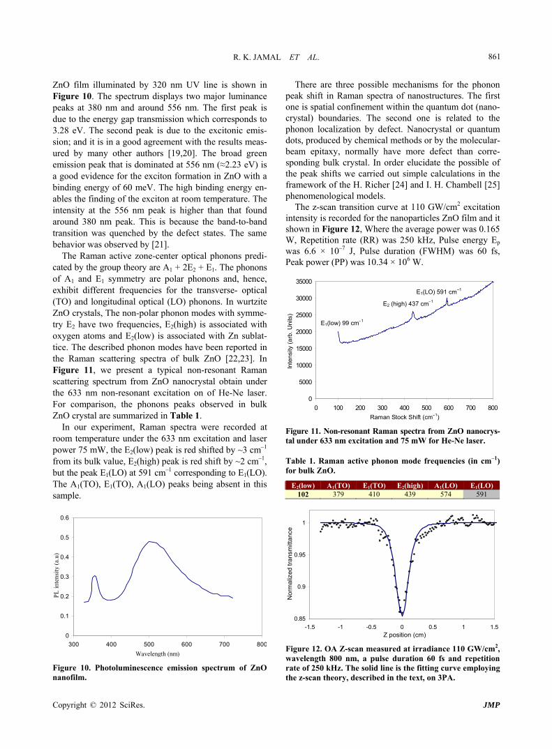
ZnO film illuminated by 320 nm UV line is shown in Figure 10. The spectrum displays two major luminance peaks at 380 nm and around 556 nm. The first peak is due to the energy gap transmission which corresponds to 3.28 eV. The second peak is due to the excitonic emis-sion; and it is in a good agreement with the results meas-ured by many other authors [19,20]. The broad green emission peak that is dominated at 556 nm (≈2.23 eV) is a good evidence for the exciton formation in ZnO with a binding energy of 60 meV. The high binding energy en-ables the finding of the exciton at room temperature. The intensity at the 556 nm peak is higher than that found around 380 nm peak. This is because the band-to-band transition was quenched by the defect states. The same behavior was observed by [21].
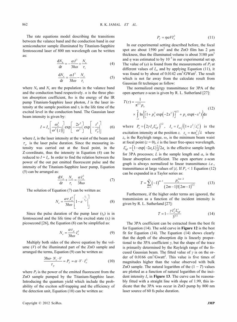
The Raman active zone-center optical phonons predi-cated by the group theory are A1 + 2E2 + E1. The phonons of A1 and E1 symmetry are polar phonons and, hence, exhibit different frequencies for the transverse- optical (TO) and longitudinal optical (LO) phonons. In wurtzite ZnO crystals, The non-polar phonon modes with symme-try E2 have two frequencies, E2(high) is associated with oxygen atoms and E2(low) is associated with Zn sublat-tice. The described phonon modes have been reported in the Raman scattering spectra of bulk ZnO [22,23]. In Figure 11, we present a typical non-resonant Raman scattering spectrum from ZnO nanocrystal obtain under the 633 nm non-resonant excitation on of He-Ne laser. For comparison, the phonons peaks observed in bulk ZnO crystal are summarized in Table 1.
In our experiment, Raman spectra were recorded at room temperature under the 633 nm excitation and laser power 75 mW, the E2(low) peak is red shifted by ~3 cm–1 from its bulk value, E2(high) peak is red shift by ~2 cm–1, but the peak E1(LO) at 591 cm–1 corresponding to E1(LO). The A1(TO), E1(TO), A1(LO) peaks being absent in this sample.
0
0.1
0.2
0.3
0.4
0.5
0.6
300 400 500 600 700 800
PL
inte
nsit
y (a
.u)
Wavelength (nm)
Figure 10. Photoluminescence emission spectrum of ZnO nanofilm.
There are three possible mechanisms for the phonon peak shift in Raman spectra of nanostructures. The first one is spatial confinement within the quantum dot (nano- crystal) boundaries. The second one is related to the phonon localization by defect. Nanocrystal or quantum dots, produced by chemical methods or by the molecular- beam epitaxy, normally have more defect than corre-sponding bulk crystal. In order elucidate the possible of the peak shifts we carried out simple calculations in the framework of the H. Richer [24] and I. H. Chambell [25] phenomenological models.
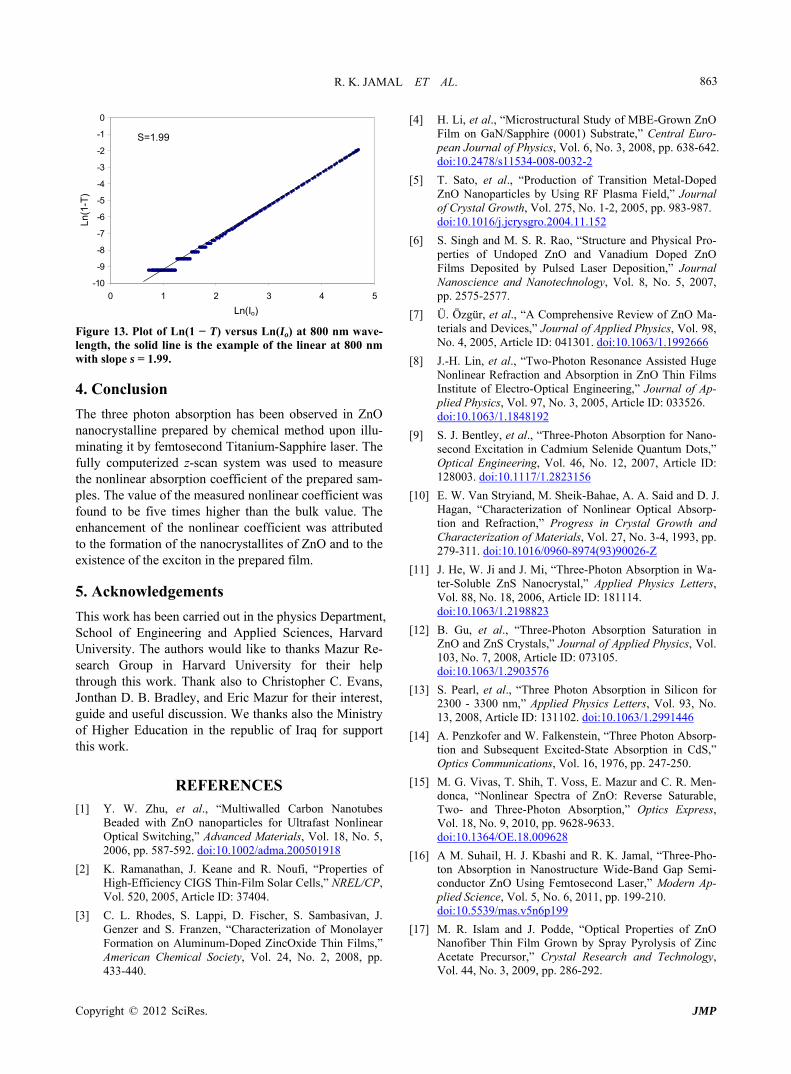
The z-scan transition curve at 110 GW/cm2 excitation intensity is recorded for the nanoparticles ZnO film and it shown in Figure 12, Where the average power was 0.165 W, Repetition rate (RR) was 250 kHz, Pulse energy Ep was 6.6 × 10⁻⁷ J, Pulse duration (FWHM) was 60 fs, Peak power (PP) was 10.34 × 10⁶ W.
0
5000
10000
15000
20000
25000
30000
35000
0 100 200 300 400 500 600 700 800
99
437
591
Inte
nsity
(a
rb.
Uni
ts)
Raman Stock Shift
–1E1(LO) 591 cm
–1 E2 (high) 437 cm
–1E1(low) 99 cm
–1(cm )
Figure 11. Non-resonant Raman spectra from ZnO nanocrys-tal under 633 nm excitation and 75 mW for He-Ne laser. Table 1. Raman active phonon mode frequencies (in cm–1) for bulk ZnO.
E2(low) A1(TO) E1(TO) E2(high) A1(LO) E1(LO)102 379 410 439 574 591
0.85
0.9
0.95
1
-1.5 -1 -0.5 0 0.5 1 1.5
Nor
mal
ized
tra
nsm
ittan
ce
Z position (cm)
Figure 12. OA Z-scan measured at irradiance 110 GW/cm2, wavelength 800 nm, a pulse duration 60 fs and repetition rate of 250 kHz. The solid line is the fitting curve employing the z-scan theory, described in the text, on 3PA.
Copyright © 2012 SciRes. JMP
R. K. JAMAL ET AL. 862
The rate equations model describing the transitions between the valance band and the conduction band in our semiconductor sample illuminated by Titanium-Sapphire femtosecond laser of 800 nm wavelength can be written as:
3
d 3h e
i
N NId
t
(4)
3
d 3e e
i
N NId
t
(5)
where Nh and Ne are the population in the valance band and the conduction band respectively. α is the three pho-ton absorption coefficient, ћω is the energy of the IR pump Titanium-Sapphire laser photon, I is the laser in-tensity at the sample position and τi is the life time of the excited level in the conduction band. The Gaussian laser beam intensity is given by:
2
2
2expo
o
2 2
2 2exp
p
r tI I
z
(6)
where Io is the laser intensity at the waist of the beam and
p is the laser pulse duration. Since the measuring in-tensity was carried out at the focal point, in the Z-coordinate, thus the intensity in Equation (4) can be reduced to I = Io. In order to find the relation between the power of the out put emitted fluorescent pulse and the intensity of the Titanium-Sapphire laser pump, Equation (5) can be arranged as:
3
d 3e e o
i
N N Id
t
(7)
The solution of Equation (7) can be written as:
3
1i
pi oIe
3eN
(8)
Since the pulse duration of the pump laser (τp) is in femtosecond and the life time of the excited state (τi) in picosecond [26], the Equation (8) can be simplified as:
3
3p
e oN I
(9)
Multiply both sides of the above equation by the vol-ume (V) of the illuminated part of the ZnO sample and arranged the terms, Equation (9) can be written as:
33 ef oP V I
3
p
N V
(10)
where Pf is the power of the emitted fluorescent from the ZnO sample pumped by the Titanium-Sapphire laser. Introducing the quantum yield which include the prob-ability of the exciton self-trapping and the efficiency of the detection unit, Equation (10) can be written as:
f oP VI (11)
In our experimental setting described before, the focal spot are about 1590 µm2 and the ZnO film has 2 µm thickness, thus the illuminated volume is about 3180 µm3 and η was estimated to by 10–5 in our experimental set up. The value of (a) is found from the measurements of Pf at different values of Io, and by applying Equation (11), it was found to by about of 0.0142 cm3/GWatt2. The result which is not far away from the calculate result from Gaussian fit technique as follow:
The normalized energy transmittance for 3PA of the open aperture z-scan is given by R. L. Sutherland [27]:
1 2
1 22 2 2
1( )
π
ln 1 exp 2 exp( ) d
o
o o
T zp
p x p x x
(12)
where 1 22 ,o o effP I L 2 21o oo oI I z z is the
2πzexcitation intensity at the position z, o o where zo is the Rayleigh range, ωo is the minimum beam waist at focal point (z = 0), λ is the laser free-space wavelength,
1 exp 2 2eff o oL a L a
is the effective sample length
for 3PA processes; L is the sample length and ao is the linear absorption coefficient. The open aperture z-scan graph is always normalized to linear transmittance i.e., transmittance at large values of |z|. If Po < 1 Equation (12) can be expanded in a Taylor series as:
2 21
1 21
12 1 ! 2 1
mm o
m
pT
m m
(13)
Furthermore, if the higher order terms are ignored, the transmission as a function of the incident intensity is given by R. L. Sutherland [27]:
2
3 21
3o effI L
T
(14)
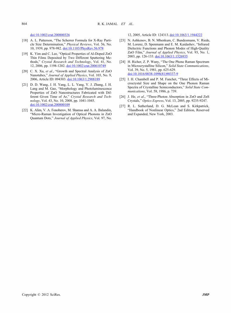
The 3PA coefficient can be extracted from the best fit for Equation (14). The sold curve in Figure 12 is the best fit for Equation (14). The Equation (14) shows clearly that the depth of the absorption dip is linearly propor-tional to the 3PA coefficient γ, but the shape of the trace is primarily determined by the Rayleigh range of the fo-cused Gaussian beam. The fitted value of γ is on the or-der of 0.0166 cm3/Gwatt2. This value is five times of magnitudes higher than the value observed with bulk ZnO sample. The natural logarithm of the (1 − T) values are plotted as a function of natural logarithm of the inci-dent intensity Io in Figure 13. The curve can be reasona-bly fitted with a straight line with slope of 1.99, this in-dicate that the 3PA was occur in ZnO pump by 800 nm laser source of 60 fs pulse duration.
Copyright © 2012 SciRes. JMP
R. K. JAMAL ET AL. 863
-10
-9
-8
-7
-6
-5
-4
-3
-2
-1
0
0 1 2 3 4 5
S=1.99
Ln(1
-T)
Ln(Io)
Figure 13. Plot of Ln(1 − T) versus Ln(Io) at 800 nm wave-length, the solid line is the example of the linear at 800 nm with slope s = 1.99.
4. Conclusion
The three photon absorption has been observed in ZnO nanocrystalline prepared by chemical method upon illu-minating it by femtosecond Titanium-Sapphire laser. The fully computerized z-scan system was used to measure the nonlinear absorption coefficient of the prepared sam-ples. The value of the measured nonlinear coefficient was found to be five times higher than the bulk value. The enhancement of the nonlinear coefficient was attributed to the formation of the nanocrystallites of ZnO and to the existence of the exciton in the prepared film.
5. Acknowledgements
This work has been carried out in the physics Department, School of Engineering and Applied Sciences, Harvard University. The authors would like to thanks Mazur Re-search Group in Harvard University for their help through this work. Thank also to Christopher C. Evans, Jonthan D. B. Bradley, and Eric Mazur for their interest, guide and useful discussion. We thanks also the Ministry of Higher Education in the republic of Iraq for support this work.
REFERENCES [1] Y. W. Zhu, et al., “Multiwalled Carbon Nanotubes
Beaded with ZnO nanoparticles for Ultrafast Nonlinear Optical Switching,” Advanced Materials, Vol. 18, No. 5, 2006, pp. 587-592. doi:10.1002/adma.200501918
[2] K. Ramanathan, J. Keane and R. Noufi, “Properties of High-Efficiency CIGS Thin-Film Solar Cells,” NREL/CP, Vol. 520, 2005, Article ID: 37404.
[3] C. L. Rhodes, S. Lappi, D. Fischer, S. Sambasivan, J. Genzer and S. Franzen, “Characterization of Monolayer Formation on Aluminum-Doped ZincOxide Thin Films,” American Chemical Society, Vol. 24, No. 2, 2008, pp. 433-440.
[4] H. Li, et al., “Microstructural Study of MBE-Grown ZnO Film on GaN/Sapphire (0001) Substrate,” Central Euro- pean Journal of Physics, Vol. 6, No. 3, 2008, pp. 638-642. doi:10.2478/s11534-008-0032-2
[5] T. Sato, et al., “Production of Transition Metal-Doped ZnO Nanoparticles by Using RF Plasma Field,” Journal of Crystal Growth, Vol. 275, No. 1-2, 2005, pp. 983-987. doi:10.1016/j.jcrysgro.2004.11.152
[6] S. Singh and M. S. R. Rao, “Structure and Physical Pro- perties of Undoped ZnO and Vanadium Doped ZnO Films Deposited by Pulsed Laser Deposition,” Journal Nanoscience and Nanotechnology, Vol. 8, No. 5, 2007, pp. 2575-2577.
[7] Ü. Özgür, et al., “A Comprehensive Review of ZnO Ma- terials and Devices,” Journal of Applied Physics, Vol. 98, No. 4, 2005, Article ID: 041301. doi:10.1063/1.1992666
[8] J.-H. Lin, et al., “Two-Photon Resonance Assisted Huge Nonlinear Refraction and Absorption in ZnO Thin Films Institute of Electro-Optical Engineering,” Journal of Ap- plied Physics, Vol. 97, No. 3, 2005, Article ID: 033526. doi:10.1063/1.1848192
[9] S. J. Bentley, et al., “Three-Photon Absorption for Nano- second Excitation in Cadmium Selenide Quantum Dots,” Optical Engineering, Vol. 46, No. 12, 2007, Article ID: 128003. doi:10.1117/1.2823156
[10] E. W. Van Stryiand, M. Sheik-Bahae, A. A. Said and D. J. Hagan, “Characterization of Nonlinear Optical Absorp- tion and Refraction,” Progress in Crystal Growth and Characterization of Materials, Vol. 27, No. 3-4, 1993, pp. 279-311. doi:10.1016/0960-8974(93)90026-Z
[11] J. He, W. Ji and J. Mi, “Three-Photon Absorption in Wa- ter-Soluble ZnS Nanocrystal,” Applied Physics Letters, Vol. 88, No. 18, 2006, Article ID: 181114. doi:10.1063/1.2198823
[12] B. Gu, et al., “Three-Photon Absorption Saturation in ZnO and ZnS Crystals,” Journal of Applied Physics, Vol. 103, No. 7, 2008, Article ID: 073105. doi:10.1063/1.2903576
[13] S. Pearl, et al., “Three Photon Absorption in Silicon for 2300 - 3300 nm,” Applied Physics Letters, Vol. 93, No. 13, 2008, Article ID: 131102. doi:10.1063/1.2991446
[14] A. Penzkofer and W. Falkenstein, “Three Photon Absorp- tion and Subsequent Excited-State Absorption in CdS,” Optics Communications, Vol. 16, 1976, pp. 247-250.
[15] M. G. Vivas, T. Shih, T. Voss, E. Mazur and C. R. Men-donca, “Nonlinear Spectra of ZnO: Reverse Saturable, Two- and Three-Photon Absorption,” Optics Express, Vol. 18, No. 9, 2010, pp. 9628-9633. doi:10.1364/OE.18.009628
[16] A M. Suhail, H. J. Kbashi and R. K. Jamal, “Three-Pho- ton Absorption in Nanostructure Wide-Band Gap Semi-conductor ZnO Using Femtosecond Laser,” Modern Ap-plied Science, Vol. 5, No. 6, 2011, pp. 199-210. doi:10.5539/mas.v5n6p199
[17] M. R. Islam and J. Podde, “Optical Properties of ZnO Nanofiber Thin Film Grown by Spray Pyrolysis of Zinc Acetate Precursor,” Crystal Research and Technology, Vol. 44, No. 3, 2009, pp. 286-292.
Copyright © 2012 SciRes. JMP
R. K. JAMAL ET AL.
Copyright © 2012 SciRes. JMP
864
doi:10.1002/crat.200800326
[18] A. L. Patterson, “The Scherrer Formula for X-Ray Parti- cle Size Determination,” Physical Reviews, Vol. 56, No. 10, 1939, pp. 978-982. doi:10.1103/PhysRev.56.978
[19] K. Yim and C. Lee, “Optical Properties of Al-Doped ZnO Thin Films Deposited by Two Different Sputtering Me- thods,” Crystal Research and Technology, Vol. 41, No. 12, 2006, pp. 1198-1202. doi:10.1002/crat.200610749
[20] C. X. Xu, et al., “Growth and Spectral Analysis of ZnO Nanotubes,” Journal of Applied Physics, Vol. 103, No. 9, 2006, Article ID: 094303. doi:10.1063/1.2908189
[21] D. D. Wang, J. H. Yang, L. L. Yang, Y. J. Zhang, J. H. Lang and M. Gao, “Morphology and Photoluminescence Properties of ZnO Nanostructures Fabricated with Dif- ferent Given Time of Ar,” Crystal Research and Tech- nology, Vol. 43, No. 10, 2008, pp. 1041-1045. doi:10.1002/crat.200800109
[22] K. Alim, V. A. Fonoberov, M. Shamsa and A. A. Balandin, “Micro-Raman Investigation of Optical Phonons in ZnO Quantum Dots,” Journal of Applied Physics, Vol. 97, No.
12, 2005, Article ID: 124313. doi:10.1063/1.1944222
[23] N. Ashkenov, B. N. Mbenkum, C. Bundesmann, V. Riede, M. Lorenz, D. Spenmann and E. M. Kaidashev, “Infrared Dielectric Functions and Phonon Modes of High-Quality ZnO Film,” Journal of Applied Physics, Vol. 93, No. 1, 2003, pp. 126-133. doi:10.1063/1.1526935
[24] H. Richer, Z. P. Wany, “The One Phone Raman Spectrum in Microcrystalline Silicon,” Solid State Communications, Vol. 39, No. 5, 1981, pp. 625-629. doi:10.1016/0038-1098(81)90337-9
[25] I. H. Chambell and P. M. Fanchet, “Three Effects of Mi-crocrystal Size and Shape on the One Phonon Raman Spectra of Crystalline Semiconductors,” Solid State Com- munications, Vol. 58, 1986, p. 739.
[26] J. He, et al., “Three-Photon Absorption in ZnO and ZnS Crystals,” Optics Express, Vol. 13, 2005, pp. 9235-9247.
[27] R. L. Sutherland, D. G. McLean and S. Kirkpatrick, “Handbook of Nonlinear Optics,” 2nd Edition, Reserved and Expanded, New York, 2003.