Embed Size (px)
Citation preview

1
Through-Silicon Via (TSV) Related Noise Coupling in Three-Dimensional (3-D)
Integrated Circuits (ICs)
A Thesis Presented
by
Mohammad Hosein Asgari
to
The Graduate School
in Partial Fulfillment of the
Requirements
for the Degree of
Master of Science
in
Electrical engineering
Stony Brook University
December 2011

ii
Stony Brook University
The Graduate School
Mohammad Hosein Asgari
We, the thesis committee for the above candidate for the
Master of Science degree, hereby recommend
acceptance of this thesis.
Prof. Emre Salman – Thesis Advisor Assistant Professor, Electrical Engineering Department
Prof. Milutin Stanavecic – Second Reader Associate Professor, Electrical Engineering Department
This thesis is accepted by the Graduate School
Lawrence Martin Dean of the Graduate School

iii
Abstract of the Thesis
Through-Silicon Via (TSV) Related Noise Coupling in Three-Dimensional (3-D)
Integrated Circuits (ICs)
by
Mohammad Hosein Asgari
Master of Science
in
Electrical Engineering
Stony Brook University
2011
As conventional integrated circuits are approaching the physical limits due to technology scaling,
alternative and complementary technologies have become a major focus. Among various
emerging technologies, three-dimensional (3-D) integration technology offers several advantages
to increase performance and functionality while reducing cost. In 3-D technologies, multiple dies
are stacked in a monolithic fashion where the communication among the dies is achieved by
vertical through-silicon vias (TSVs). Despite important advantages, 3-D integration has certain
challenges that need to be addressed. In this thesis, noise coupling due to TSVs, an important
issue that degrades signal integrity, is investigated. Compact models are proposed to analyze
TSV related noise coupling for different TSV types such as via-first and via-last, and different
substrate grounding topologies. Figures-of-merit and design guidelines are also developed to
ensure reliable 3-D circuits in the presence of TSV related noise coupling.

iv
Table of Contents
Chapter 1 – Introduction …………………………………………………………… 1
Chapter 2 – Three-Dimensional (3-D) Integration Technology …………………… 3
Chapter 3 – Models for Through-Silicon Via (TSV) and Substrate …………… 6
Chapter 4 – Proposed Compact Models and Verification …………………… 11
Chapter 5 – Analysis Results and Discussion …………………………………… 32
Chapter 6 – Conclusions …………………………………………………………… 35
Chapter 7 – Future Work …………………………………………………………… 36
References …………………………………………………………………………… 37

v
List of Abbreviations
IC – Integrated Circuit
TSV – Through Silicon Via
GND - Ground
VIC – Victim
SUB - Substrate
CMOS – Complementary Metal-Oxide-Semiconductor
VLSI – Very Large Scale Integrated Circuit

1
Chapter 1 - Introduction
Since 1960, the integrated circuit (IC) industry aims to increase the performance and
functionality of ICs while reducing power dissipation and manufacturing cost. This goal has
primarily been achieved by means of technology scaling and enhancing system-level design
techniques.
ITRS predicts that the physical limits of technology scaling will be reached by 2020 [1].
Numerous efforts exist to develop novel technologies alternative to conventional 2-D
complementary metal-oxide semiconductor (CMOS) ICs. Carbon nanotubes, graphene based
circuits, and single electron devices are examples of these efforts at the device level [2]. At the
technology level, an emerging opportunity that that has received considerable attention is 3-D
ICs [9,10]. 3-D integration technology is highly compatible with existing CMOS manufacturing
processes, thereby making 3-D technology a favorable candidate in the IC industry. Furthermore,
3-D integration is highly synergistic with conventional CMOS technology.
An important signal integrity issue in 3-D ICs is discussed in this thesis. 3-D technologies
require through-silicon vias (TSVs) to transmit power, data, and clock signals among stacked
dies. Since these TSVs need to pass through the substrate of the dies, noise is injected into the
substrate due to the capacitive coupling between a TSV and substrate. This noise reaches the
surrounding victim transistors that have a substrate bulk connection on the same plane. The
amount of noise that reaches these transistors depends on several parameters. A good
understanding of these parameters and the complex relationship between an aggressor TSV and
the victim transistor is critical in maintaining a reliable operation with enhanced signal integrity.

2
This thesis consists of seven chapters. The significance of 3-D integration technology as an
emerging opportunity is explained in Chapter 2. In Chapter 3, the substrate is modeled using a
distributed network of resistors and capacitors (RC mesh). In Chapter 4, an equivalent compact
model is proposed to reduce the computational complexity of the aforementioned distributed
model while maintaining a reasonable accuracy. This model is verified by comparing the noise
results with the results obtained from a more complicated distributed RC mesh network. The
analysis results based on the proposed model are presented in Chapter 5. These results are also
discussed with emphasis on the effect of different TSV types and grounding configurations on
noise. Important conclusions are summarized in Chapter 6. Finally, possible future work is
mentioned in Chapter 7.

3
Chapter 2 – Three-Dimensional (3-D) Integration Technology
In 3-D ICs multiple wafers are vertically stacked where the communication among the wafers is
achieved by TSVs.
Figure 1 ‐ TSV and substrate on a 3‐D circuit.
The primary issue in 2-D ICs is increasing global interconnect lengths and related issues such as
global signaling and power consumption. Continuous scaling of the transistors reduces the gate
delays, but the global delay of the interconnect increases. A reduction in the length of a global
interconnect is therefore required. 3-D integration provides this reduction by stacking multiple
dies in a monolithic fashion. Furthermore, total active power of a 2-D circuit is considerably
reduced when utilizing 3-D integration technology [3]. Another advantage of 3-D integration
technology is the reduction on the physical area of the dies which is of special interest for
medical, portable, and military applications. 3-D integration is therefore a prominent candidate to
TSV Substrate
Plane 1
Plane 2

4
continue the benefits of technology scaling. To produce a reliable 3-D circuit, multiple aspects of
this new technology need to be investigated.
A critical issue in 3-D circuits is the communication between planes, as achieved by TSVs. The
effect of TSVs on the design process of a 3-D circuit has been investigated in the literature[9].
There are several options to fabricate 3-D circuits. The orientation of the planes can be back-to-
face, and face-to-face as illustrated respectively in Figures 2 and 3. Furthermore, there are two
types of TSV fabrication techniques. Depending upon when the TSV is fabricated, the TSV
technology is referred to as via-first, via-middle or via-last. The effect of these different TSVs on
the circuit design process needs to be investigated. In this thesis, the effect of different TSV
fabrication methods on noise coupling is addressed, as further discussed in Chapter 4.
An important challenge in 3-D circuits is the TSV induced substrate noise . This issue is a
significant challenge in 3-D circuits since the TSVs pass through the substrate and inject
undesirable noise signals into the substrate due to capacitive coupling between the TSV and
substrate.
Figure 2 – Face‐to‐back orientation.
5
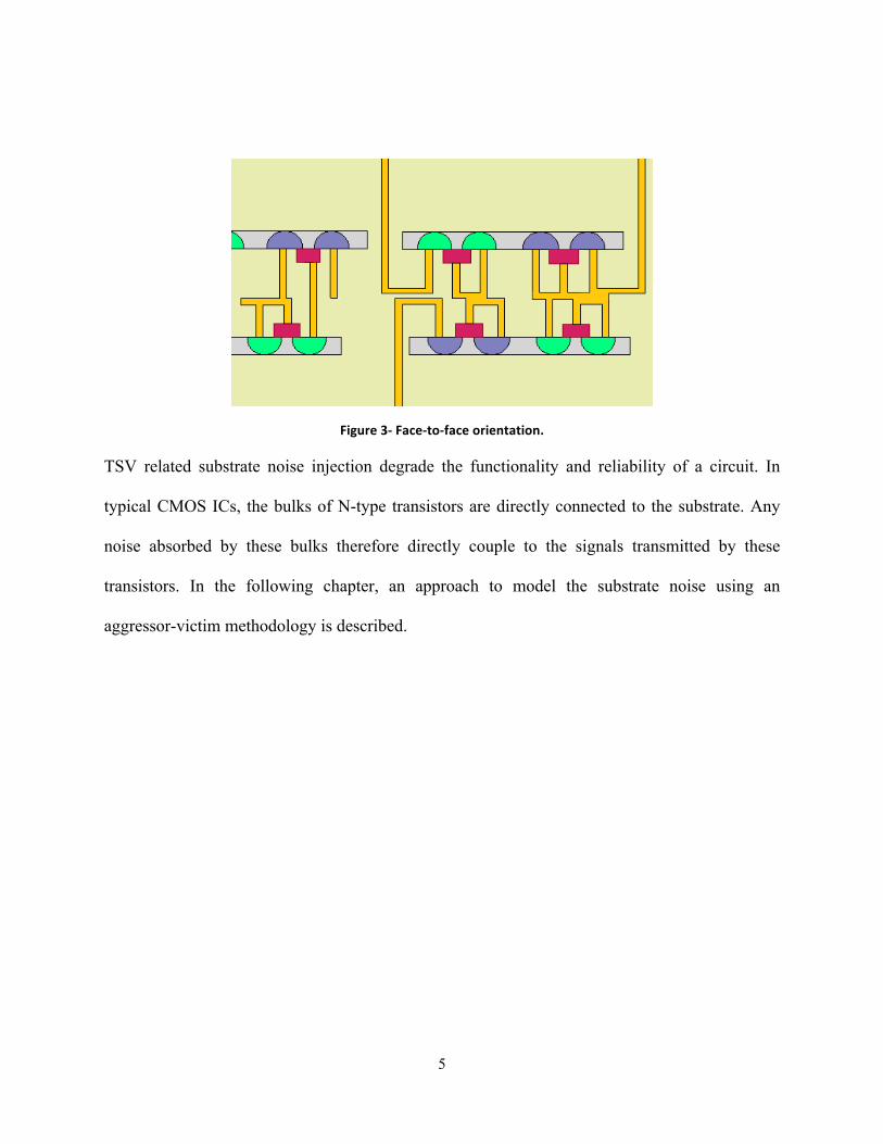
Figure 3‐ Face‐to‐face orientation.
TSV related substrate noise injection degrade the functionality and reliability of a circuit. In
typical CMOS ICs, the bulks of N-type transistors are directly connected to the substrate. Any
noise absorbed by these bulks therefore directly couple to the signals transmitted by these
transistors. In the following chapter, an approach to model the substrate noise using an
aggressor-victim methodology is described.

6
Chapter 3 - Models for Through-Silicon Via (TSV) and Substrate
The first step in analyzing the TSV related noise coupling is to determine an aggressor and
victim. The aggressor, which is the source of noise, is in this case the TSV. The analysis is
performed for two TSV fabrication techniques: via-first and via-last. As mentioned previously,
these two methods differ in TSV filling material and substrate thickness, which effects the
physical dimensions of the TSVs. Thus, the effect of the TSV and the corresponding noise
characteristics are different.
To understand TSV related noise propagation, the TSV and substrate behavior need to be
modeled. TSV and substrate models have received considerable attention in the literature [4-6].
A typical TSV and substrate model described in [4] is adopted in this work.
3.1 TSV Model
As described in [4], a TSV is represented with parasitic resistors, inductors and capacitors to the
substrate as illustrated in Figure 5. The resistance and inductance represent the conductive
characteristics of the TSV whereas the parasitic capacitance represents the dielectric layer
between the TSV and the substrate. The TSV resistance (RTSV) , the TSV capacitance (CTSV) and
the TSV inductance (LTSV) are determined by

7
Figure 4 ‐ TSV model [8].
where ρf, ε0, µ0, DTSV, WTSV and tdie represent, respectively, conductivity of the filling material,
permittivity of the dielectric layer, vacuum permeability, TSV depth, TSV diameter, and
dielectric thickness. These parameters are also illustrated in Figure 4.
3.2 Substrate Model
The substrate is modeled by a network of admittances, as depicted in Figure 6. In this model, the
substrate is discretized into a large number of cuboids where each cuboid is modeled with six
pairs of parallel RCs. The unit resistance RS and the unit capacitance CS of a cuboid are
determined by

8
Figure 5 ‐ Substrate model [8].
where ρs, εs, dc refer, respectively, substrate resistivity, substrate dielectric permittivity and the
unit length of a cuboid.
The TSV parameters illustrated in Figure 3 are dependent on the type of TSV. For example, in
via-first TSVs, the filling material is polysilicon whereas in via-last TSVs copper is used as the
filling material. Thus the resistivity of the filling material in both cases in significantly different.
Using these building blocks, a distributed RC mesh is obtained to model the substrate. Four cases
are investigated to analyze TSV related noise coupling:
• Case 1: Via-first with custom single contact
• Case 2:Via-first with preplaced substrate contacts
• Case 3: Via-last with custom single contact.
• Case 4: Via-last with preplaced substrate contacts

9
Figure 6 ‐ Distributed RC mesh.
A portion of the substrate modeled by utilizing a distributed RC mesh is illustrated in Figure 6.
The top view of the same distributed RC mesh is illustrated in Figure 7.
Figure 7 ‐ Distributed RC mesh, top view.
The distributed RC mesh is a complicated network that captures the noise propagation through
the substrate. A primary disadvantage of this model is the high computational complexity which
becomes prohibitive in analyzing practical circuits with thousands of transistors. Thus, in this
thesis, an equivalent compact model is developed to represent TSV related noise coupling. This

10
compact model is utilized to determine a safe distance between an aggressor TSV and the victim
transistor beyond which the coupling noise becomes intolerable. The proposed equivalent model
is described in the following chapter.

11
Chapter 4 – Proposed Compact Models and Verification
In the proposed model, the entire substrate network is represented by a two-port network. If the
RC elements of this two-port network have negligible variation across the frequency range of
interest, the reduced model can replace the more complicated substrate network described in the
previous chapter. Choosing an appropriate circuit model for the two-port network is critical to
obtain sufficient accuracy. Unless an appropriate model is chosen, negative impedances or
undesirable variations across frequency can occur.
Two different models are investigated, as illustrated, respectively, in Figures 8 and 9. In each
model, the equivalent L_TSV, R_TSV, and C_TSV represent the TSV parasitic impedances as
described in Chapter 3. In the first model, an equivalent L-circuit model is utilized. The
admittances Y_SUB and Y_GND consist of a parallel RC circuit. These admittances are obtained
by performing two sets of single port AC simulations of the substrate network. This analysis is
achieved by using the S-parameter simulation environment provided by Virtuoso Cadence [8].
Note that R_VIC in Figures 8 and 9 represents the ground configuration for the victim node such
as a guard ring placed around the victim circuit. Also note that C_Load refers to the load
capacitance of a TSV. For example, for a clock TSV this capacitance is determined by the
number of registers that this TSV drives.
After analyzing the results, it is observed that the L-circuit cannot produce sufficiently accurate
results. This inaccuracy is due to the inability of the L-circuit model to consider substrate
contacts located in the vicinity of the victim node. The second model, however, is a sufficiently
accurate representation of this phenomenon, as described below.

12
The primary difference between these two models is the representation of the equivalent
substrate network. In the second model, referred to as the pi-circuit model, an additional
admittance Y_VIC exists between the victim node and ground. Similar to the first model, the
equivalent admittances are obtained by performing two port ac simulation of the substrate.
Figure 8 ‐ Substrate L equivalent circuit.
As mentioned previously, the L-circuit model cannot consider the effect of guard rings placed
close to the victim node. Such guard rings filter the noise and prevent the noise from reaching the
victim, a mechanism similar to a Faraday cage. In the L-circuit model, however, any noise
current that does not propagate toward the ground contact, propagates straight to the victim node
since no other path exists for the current to flow. Furthermore, although this model represents the
substrate network reasonably well, provided that the ground connection is located far from the
TSV, another source of inaccuracy exists. This additional error is due to the fact that the two
equivalent admittances are interdependent since the substrate network is common to both
admittances. This characteristic is not considered in the L-circuit model. Due to these reasons, a
pi-circuit model is developed for the equivalent two port network.
CLoad

13
The pi-circuit model consists of three admittances, Y_GND, Y_SUB and Y_VIC as illustrated in
Figure 9. This model is more appropriate in modeling the substrate. Since, the current that flows
toward the victim has an additional path to the ground, represented by YVIC. Thus YVIC can model
the effect of typical noise reduction techniques such as guard rings.
Figure 9 ‐ Substrate Pi‐equivalent circuit.
Theoretically, the Y-parameters of the pi-circuit model can be matched to the more complicated
substrate network represented as a 3-D RC mesh. This procedure includes obtaining frequency
dependant elements for the pi-circuit model. This dependence on frequency, however, is
negligible in the frequency range of interest. The maximum change in the RC elements is less
than 0.1%. Thus, a single RC value is chosen for each Y_GND, Y_SUB and Y_VIC
A two-port system can be characterized by utilizing Y parameters. These Y parameters, Y11, Y12,
Y21 and Y22 are described by the following equations
CLoad
VX VY

14
Where I1, V1, I2 and V2 are, respectively, input current, input voltage, output current and output
voltage. To obtain an accurate equivalent model, the Y parameters of the proposed pi-circuit
model should be matched to the Y parameters obtained from the more complicated RC mesh
network (illustrated in Figure 6). Referring to Figure 10, the Y parameters of the proposed circuit
model are determined as follows
Figure 10 – pi‐circuit to determine Y parameters.
Port 1 Port 2

15
These Y parameters are utilized to obtain the transfer function of the substrate represented by the
pi-circuit model. The following five equations describe the steps in obtaining the
transconductance, G(s), of the system
where the denominator of B is
,
,
,
,
.

16
To evaluate the accuracy of the proposed equivalent pi-circuit model, the transconductance
described is compared with the transconductance obtained from the distributed RC mesh
network. The results of this comparison are illustrated in Figure 11.
Figure 11 ‐ Distributed RC mesh transfer function (dashed). Equivalent pi model transfer function (solid).
As depicted in this figure, the transconductance obtained from these two networks are
sufficiently close.
After obtaining an equivalent pi-circuit model to represent the complicated substrate network, in
the next step, a relationship between the Y parameters of the equivalent network and the physical
distance between the TSV victim and ground nodes is investigated. This relationship is highly
critical to obtain as a that determines the physical area where transistors should be placed. An

17
accurate characterization of the safe distance is significant for certain applications such as 3-D
core memory stacks and heterogeneous 3-D ICs where highly sensitive analog/RF blocks coexist
with aggressor TSVs.
To find a relationship between Y_SUB, Y_GND, Y_VIC, and the physical distances, a series of
simulations are performed for different cases. The large amount of data obtained by these
simulations are represented by specific functions with two variables. These different cases are
described in the following:
Case 1: Via-first TSV with a single custom ground node
In this case, d1 (µm) and d2 (µm) refer respectively to the distance between the TSV and the
victim node, and the distance between the TSV and ground.
The appropriate fitting function used to model the dependence of RC elements on distance is
F (d1, d2) = A + E.d1 + B.ln(d1) + C.d2 + D.ln(d2)
where A, B, C, D, and E are fitting coefficients. This fitting function is obtained after thorough
simulations of the distributed RC mesh network. These results represent the dependence of Y
elements on distance and are illustrated in Figures [12-18]. For example, the dependence of
Y_GND R_GND, and C_GND on the two distances is illustrated in Figures 12 and 15. Similarly,
the remaining elements of the Y parameters are illustrated in Figures [12-17].

18
Figure 12 ‐ Case 1, C_GND vs. d1 and d2.
Figure 13 ‐ Case 1, C_SUB vs. d1 and d2.

19
Figure 14 ‐ Case 1, C_VIC vs. d1 and d2.
Figure 15 ‐ Case 1, 1000/R_GND vs. d1 and d2.

20
Figure 16‐Case 1, 1000/R_SUB vs. d1 and d2.
Figure 17 ‐ Case 1, R_VIC vs. d1 and d2.
21
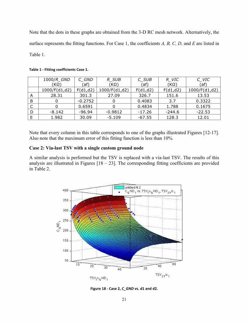
Note that the dots in these graphs are obtained from the 3-D RC mesh network. Alternatively, the
surface represents the fitting functions. For Case 1, the coefficients A, B, C, D, and E are listed in
Table 1.
Table 1 ‐ Fitting coefficients Case 1.
1000/R_GND
(KΩ) C_GND
(af) R_SUB (KΩ)
C_SUB (af)
R_VIC (KΩ)
C_VIC (af)
1000/F(d1,d2) F(d1,d2) 1000/F(d1,d2) F(d1,d2) F(d1,d2) 1000/F(d1,d2) A 28.31 301.3 27.09 326.7 151.6 13.53 B 0 -0.2752 0 0.4083 3.7 0.3322 C 0 0.6591 0 0.4834 1.788 0.1675 D -8.142 -96.94 -0.9812 -17.26 -244.6 -22.53 E 1.982 30.09 -5.109 -67.55 128.3 12.01
Note that every column in this table corresponds to one of the graphs illustrated Figures [12-17]. Also note that the maximum error of this fitting function is less than 10%.
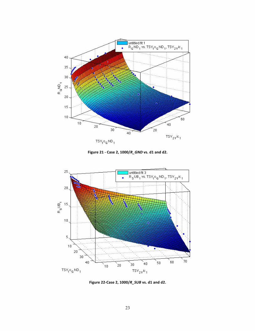
Case 2: Via-last TSV with a single custom ground node
A similar analysis is performed but the TSV is replaced with a via-last TSV. The results of this analysis are illustrated in Figures [18 – 23]. The corresponding fitting coefficients are provided in Table 2.
Figure 18 ‐ Case 2, C_GND vs. d1 and d2.

22
Figure 19 ‐ Case 2, C_SUB vs. d1 and d2.
Figure 20 ‐ Case 2, C_VIC vs. d1 and d2.
23
Figure 21 ‐ Case 2, 1000/R_GND vs. d1 and d2.
Figure 22‐Case 2, 1000/R_SUB vs. d1 and d2.

24
Figure 23 ‐ Case 2, R_VIC vs. d1 and d2.
Table 2 ‐ Fitting coefficients Case 2.
1000/R_GND
(KΩ) C_GND (af)
R_SUB (KΩ)
C_SUB (af)
R_VIC (KΩ)
C_VIC (af)
1000/F(d1,d2) F(d1,d2) 1000/F(d1,d2) F(d1,d2) F(d1,d2) 1000/F(d1,d2) A 34.37 263.7 27.97 298.5 9.117 101.4 B 0.135 0.7956 ‐0.07299 0 0 0.1799 C 0 ‐1.129 ‐0.06895 ‐0.7594 0.04936 0.5132 D 1.7 50.72 ‐1.436 ‐16.34 ‐3.465 ‐37.48 E ‐8.623 ‐77.3 ‐1.816 ‐14.91 1.82 17.89

25
Case 3: :Via-first with preplaced substrate contacts
A similar analysis is performed with a via-first TSV, but the single ground connection is replaced with preplaced substrate contacts. The results of this analysis are illustrated in Figures [24 – 29]. The corresponding fitting coefficients are provided in Table 3.
Figure 24‐Case 3, C_GND vs. d1 and d2.
Figure 25‐Case 3, C_SUB vs. d1 and d2.

26
Figure 26‐Case 3, C_VIC vs. d1 and d2.
Figure 27‐Case 3, R_GND vs. d1 and d2.

27
Figure 28‐Case 3, R_SUB vs. d1 and d2.
Figure 29‐Case 3, R_VIC vs. d1 and d2.

28
Table 3 ‐ Fitting coefficients Case 3.
1000/R_GND (KΩ)
C_GND (af)
R_SUB (KΩ)
C_SUB (af)
R_VIC (KΩ)
C_VIC (af)
1000/F(d1,d2) F(d1,d2) 1000/F(d1,d2) F(d1,d2) F(d1,d2) 1000/F(d1,d2) A 28.87 101.4 263.7 298.5 9.117 101.4 B 0.446 0.1799 0.5789 0 0 0.132 C 0.0182 0.5132 ‐1.129 ‐0.7594 0.04936 0.37.87 D ‐1.737 ‐37.48 50.72 ‐16.34 ‐3.465 ‐28.4 E 8 17.9 ‐77.3 ‐14.91 1.82 18.89
Case 4: :Via-last with preplaced substrate contacts
A similar analysis is performed with a via-last TSV and preplaced substrate contacts. The results of this analysis are illustrated in Figures [30 – 35]. The corresponding fitting coefficients are provided in Table 4.
Figure 30‐Case 4, C_GND vs. d1 and d2.

29
Figure 31‐Case 4, C_SUB vs. d1 and d2.
Figure 32‐Case 4, C_VIC vs. d1 and d2.

30
Figure 33‐Case 4, 1000/R_GND vs. d1 and d2.
Figure 34‐Case 4, 1000/R_SUB vs. d1 and d2.

31
Figure 35‐Case 4, R_VIC vs. d1 and d2.
Table 4 ‐ Fitting coefficients Case 4.
1000/R_GND (KΩ)
C_GND (af)
R_SUB (KΩ)
C_SUB (af)
R_VIC (KΩ)
C_VIC (af)
1000/F(d1,d2) F(d1,d2) 1000/F(d1,d2) F(d1,d2) F(d1,d2) 1000/F(d1,d2) A 14.74 67.4 309.8 276.5 3.1 276.5 B 0.333 0.16 0.0789 0.118 0 0 C 0 0.532 ‐0.971 ‐0.6835 0 0.87 D ‐0.86 ‐26.48 61.2 ‐13.4 ‐6.899 ‐48.99 E 4.7 8.9 ‐7.56 ‐24.3 4.36 20.34

32
Chapter 5 – Analysis Results and Discussion
Equivalent models are obtained for the four cases as described in the previous chapter. These
models are helpful to analyze noise coupling and determine the advantages and limitations of
different types of TSVs and ground contact placements. These results provide valuable
guidelines to produce reliable 3-D ICs with enhanced signal integrity.
The noise coupling characteristics of via-first and via-last TSVs are compared in Figure 36 when
there is only a single ground connection between the TSV and the victim. As shown in this
figure, via-last TSVs inject greater noise as compared to via-first TSVs. Similarly, with
preplaced substrate contacts in the circuit, the magnitude of the noise transfer function is higher
for via-last, as illustrated in Figure 37. This result is due to the higher TSV diameter and depth.
A higher diameter and depth significantly increases the TSV capacitance. Furthermore, a greater
depth reduces the substrate resistance thereby increasing the noise that couples to the victim.
Figure 36 ‐ Noise transfer function, custom single ground.
Via‐last
Via‐first

33
Another important factor in determining noise behavior is the placement of ground contacts on
the substrate. The dependence of noise coupling on the distance between TSV and ground
contact is illustrated in Figure 37 in time domain for both via first and via last TSVs, where a
time domain analysis is performed. Depending on noise constraints, the peak and RMS noise can
be important design objectives. Using the transfer function, the peak noise can be obtained by
multiplying the FFT of the input signal with the transfer function and transforming the result
back to the time domain. The results obtained from this procedure are the same as transient
analysis results.
Figure 37 ‐ Noise transfer function, pre‐placed ground node.
Via‐last
Via‐first

34
As illustrated in Figure 38, the noise that couples to the victim initially increases with increasing
distance between TSV and ground contact. After a certain point however, the increase in the
noise is marginal. Another important conclusion from this figure is that the dependence of noise
on distance is stronger for the via-last TSVs. Thus, in via-last TSVs, placing a ground contact
sufficiently close to the TSV is important to reduce noise.
Figure 38 ‐ RMS noise comparison vs. TSV‐GND distance. Via‐last, Via‐first.
0 2.5 5 7.5 10 12.5
TSV‐GND Distance
Via‐last
Via‐first
35
Chapter 6 – Conclusions
Among the emerging IC technologies, 3-D integration is widely recognized as a potential
candidate to continue technology scaling. This technology utilizes TSVs to transmit data, power,
and clock signals to different planes. An adverse effect of the TSVs is noise injection into the
substrate. This effect is modeled in this thesis and related design guidelines are provided.
To model the substrate, a complicated distributed network of resistors and capacitors is used as a
reference. To model TSV related noise coupling, four different cases are investigated (via-first
TSV with a single custom ground connection, via-last TSV with a single custom ground
connection, via-first TSV with a distributed ground pattern, and via-last TSV with a distributed
ground pattern). Compact equivalent models based on a pi-circuit are developed for each case.
The developed noise transfer functions are utilized to investigate the noise characteristics of via-
first and via-last TSVs and different ground contact configurations. The proposed models can
also be used to determine a safe distance around an aggressor TSV. This safe distance depends
on the tolerable noise which is determined by the type and functionality of the circuit. This thesis
provides design guidelines to avoid TSV related noise coupling and enhance reliability in 3-D
ICs.

36
Chapter 7 – Future Work
This work can be expanded in several ways. Reliability is a primary concern in nanoscale
technologies where the effect of environmental variations such as noise is significant. In dense 3-
D circuits, TSV related noise coupling can cause detrimental issues. Using the method described
in this thesis, TSV related noise coupling can be efficiently analyzed and the effect of noise can
be investigated in specialized circuits such as core-memory stacks and 3-D integrated
implantable biomedical circuits.
Another topic that can be further explored is the efficiency of various noise reduction
methodologies. For example, the effect of guard rings in suppressing TSV related noise can be
modeled for different ring dimensions and topologies. Furthermore, utilizing power and ground
TSVs to shield noise can be explored to further minimize noise coupling.

37
References
[1] The International Technology Roadmap for Semiconductors (ITRS), www.ITRS.net, 1999.
[2] Ph. Avouris, J. Appenzeller, R. Martel, and S.J. Wind, "Carbon nanotube electronics," Proceedings of the IEEE, Vol. 91, No. 11, November 2003.
[3] S. F. Al‐Sarawi, D. Abbott, and P. D. Franzon, ‘‘A Review of 3‐D Packaging Technology,’’ IEEE Trans. Components, Pkg. & Manufacturing Technology, Vol. 21 , No. 1, 1998.
[4] J. Cho, J. Shim, E. Song, J. S. Pak, J. Lee, H. Lee, K. Park, J. Kim, "Active circuit to through silicon via
(TSV) noise coupling," IEEE Proc. Electrical Performance of Electronic Packaging and Systems, Pages: 97 ‐ 100, Oct. 2009.
[5] X. Duan, X. Gu, J. Cho, J. Kim, "A through‐silicon‐via to active device noise coupling study for CMOS SOI technology", Electronic Components and Technology Conference (ECTC), Pages: 1791 – 1795, 2011
[6] K. Yoon, G. Kim, W. Lee, T. Song and J. Kim, "Modeling and Analysis of Near‐End Crosstalk Between
TSVs, Metal Interconnects and RDLs in TSV‐based 3D IC and Silicon Interposer," Electronic Packaging Technology Conference, 2009.
[7] E. Salman, M. H. Asgari, M. Stanacevic, “Signal integrity analysis of a 2‐D and 3‐D integrated potentiostat for neurotransmitter sensing,” Biomedical Circuits and Systems Conference (BioCAS), 2011.
[8] [Online] http://www.cadence.com/
[9] V. Pavlidis, E. G. Friedman, “Three‐dimensional integrated circuit design,” Morgan Kaufmann, 2009.
[10] Knickerbocker, J. U., et.al., “Three‐dimensional silicon integration,” IBM Journal of Research and
Development, 2008.